experimental investigations of laser-induced forward transfer process of organic thin films
TRANSCRIPT

Experimental investigations of laser-induced forward transfer
process of organic thin films
Benjamin Thomas a, Anne Patricia Alloncle a,*, Philippe Delaporte a, Marc Sentis a,Sebastien Sanaur b, Michael Barret b, Philippe Collot b
a Laboratoire Laser Plasma et Procedes Photoniques (LP3), UMR 6182 CNRS - Universite de la Mediterranee,
Cs 917 13288 Marseille Cedex 9, Franceb Centre de Microelectronique de Provence (CMP-GC), Ecole de Mines de St ETienne, Department of Packaging
and Flexible Substrates (PS2), 13541 Gardanne, France
Received 9 June 2007; received in revised form 14 September 2007; accepted 14 September 2007
Available online 21 September 2007
Abstract
This paper deals with transfer induced by laser of thin layers of a conducting polymer, the poly(3,4-ethylenedioxythiophene)-poly(styr-
enesulfonate), for applications in plastic electronics. This relatively simple technique of direct writing offers the ability to make surface micro-
patterning by localized deposits of material. The study of the various mechanisms (ablation, transfer and deposit) has been carried out according to
different conditions of irradiation: wavelength (from ultraviolet to infrared radiation), pulse duration (nanosecond and sub-nanosecond) and
fluence. The morphology of the transferred patterns has been analyzed by optical microscopy and scanning electronic microscopy. Our objective is
to understand the different mechanisms involved in the process in order to optimize it in terms of geometrical resolution while preserving the
properties of the transferred material.
# 2007 Elsevier B.V. All rights reserved.
www.elsevier.com/locate/apsusc
Available online at www.sciencedirect.com
Applied Surface Science 254 (2007) 1206–1210
Keywords: LIFT; Polymer; Ablation; Transfer; Laser
1. Introduction
Some applications in microelectronics are concerned by a
mass production requiring reduced manufacturing costs and a
high rate of manufacture. It is for example the production of
objects with simple electronic functionalities used in fields such
as radio frequency identification (RFID) tags, smart card or
micro-connecting systems.
The development of the direct printing technologies of the
components on flexible supports, associated with the use of
new conductive polymeric materials would allow avoiding the
use of complex and expensive techniques such as photolitho-
graphy.
The main process which is currently used is a printing
technique, similar to ink-jet techniques. It requires the
solubility of the organic material to deposit. New organic
compounds with very interesting electric characteristics are
* Corresponding author. Tel.: +33 491 829 381; fax: +33 491 829 289.
E-mail address: [email protected] (A.P. Alloncle).
0169-4332/$ – see front matter # 2007 Elsevier B.V. All rights reserved.
doi:10.1016/j.apsusc.2007.09.042
regularly synthesized, and numbers of them do not have the
solubility properties which would enable them to be used by
this printing process. It is thus very interesting to study the
implementation of new techniques giving the possibility to
produce electronic components with non-soluble organic
materials on flexible supports.
The objective of the works presented here is to study the
potential of laser techniques in plastic microelectronics.
Particularly, the LIFT (laser-induced forward transfer) process
of a conducting polymer already used in ink-jet printing
technique: the PEDOT-PSS (poly(3,4-ethylenedioxythio-
phene)-poly(styrenesulfonate)).
2. Description of the experiments
The laser-induced forward transfer (LIFT) technique
consists in removing a small piece of a thin layer previously
deposited on a transparent substrate and transferring it on
another substrate using a pulsed laser (Fig. 1). This simple,
single step, direct printing technique offers the ability to make
surface micro-patterning or localized deposition of material.
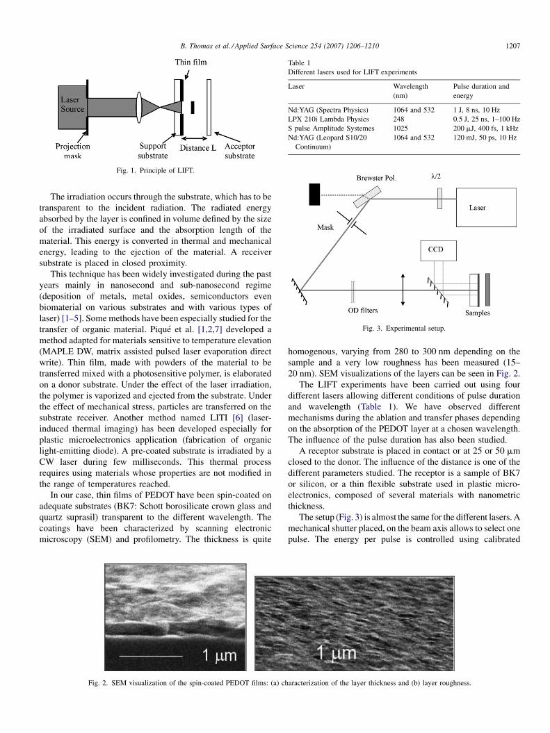
Fig. 1. Principle of LIFT.
Fig. 3. Experimental setup.
Table 1
Different lasers used for LIFT experiments
Laser Wavelength
(nm)
Pulse duration and
energy
Nd:YAG (Spectra Physics) 1064 and 532 1 J, 8 ns, 10 Hz
LPX 210i Lambda Physics 248 0.5 J, 25 ns, 1–100 Hz
S pulse Amplitude Systemes 1025 200 mJ, 400 fs, 1 kHz
Nd:YAG (Leopard S10/20
Continuum)
1064 and 532 120 mJ, 50 ps, 10 Hz
B. Thomas et al. / Applied Surface Science 254 (2007) 1206–1210 1207
The irradiation occurs through the substrate, which has to be
transparent to the incident radiation. The radiated energy
absorbed by the layer is confined in volume defined by the size
of the irradiated surface and the absorption length of the
material. This energy is converted in thermal and mechanical
energy, leading to the ejection of the material. A receiver
substrate is placed in closed proximity.
This technique has been widely investigated during the past
years mainly in nanosecond and sub-nanosecond regime
(deposition of metals, metal oxides, semiconductors even
biomaterial on various substrates and with various types of
laser) [1–5]. Some methods have been especially studied for the
transfer of organic material. Pique et al. [1,2,7] developed a
method adapted for materials sensitive to temperature elevation
(MAPLE DW, matrix assisted pulsed laser evaporation direct
write). Thin film, made with powders of the material to be
transferred mixed with a photosensitive polymer, is elaborated
on a donor substrate. Under the effect of the laser irradiation,
the polymer is vaporized and ejected from the substrate. Under
the effect of mechanical stress, particles are transferred on the
substrate receiver. Another method named LITI [6] (laser-
induced thermal imaging) has been developed especially for
plastic microelectronics application (fabrication of organic
light-emitting diode). A pre-coated substrate is irradiated by a
CW laser during few milliseconds. This thermal process
requires using materials whose properties are not modified in
the range of temperatures reached.
In our case, thin films of PEDOT have been spin-coated on
adequate substrates (BK7: Schott borosilicate crown glass and
quartz suprasil) transparent to the different wavelength. The
coatings have been characterized by scanning electronic
microscopy (SEM) and profilometry. The thickness is quite
Fig. 2. SEM visualization of the spin-coated PEDOT films: (a) ch
homogenous, varying from 280 to 300 nm depending on the
sample and a very low roughness has been measured (15–
20 nm). SEM visualizations of the layers can be seen in Fig. 2.
The LIFT experiments have been carried out using four
different lasers allowing different conditions of pulse duration
and wavelength (Table 1). We have observed different
mechanisms during the ablation and transfer phases depending
on the absorption of the PEDOT layer at a chosen wavelength.
The influence of the pulse duration has also been studied.
A receptor substrate is placed in contact or at 25 or 50 mm
closed to the donor. The influence of the distance is one of the
different parameters studied. The receptor is a sample of BK7
or silicon, or a thin flexible substrate used in plastic micro-
electronics, composed of several materials with nanometric
thickness.
The setup (Fig. 3) is almost the same for the different lasers. A
mechanical shutter placed, on the beam axis allows to select one
pulse. The energy per pulse is controlled using calibrated
aracterization of the layer thickness and (b) layer roughness.
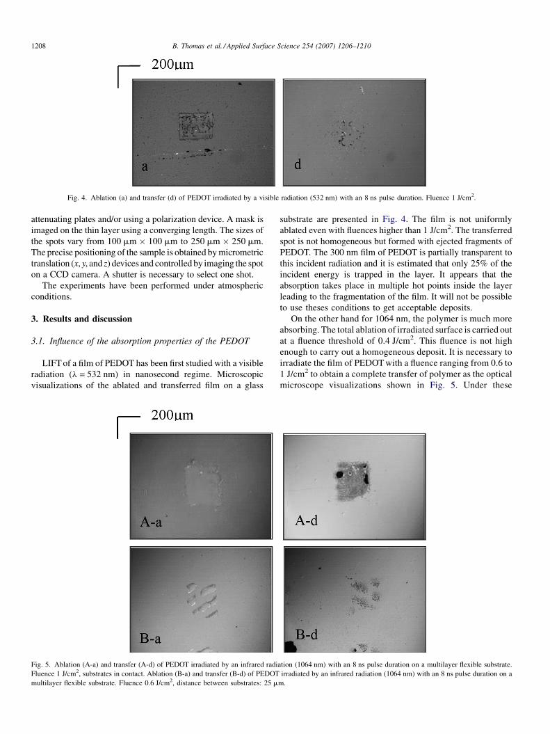
Fig. 4. Ablation (a) and transfer (d) of PEDOT irradiated by a visible radiation (532 nm) with an 8 ns pulse duration. Fluence 1 J/cm2.
B. Thomas et al. / Applied Surface Science 254 (2007) 1206–12101208
attenuating plates and/or using a polarization device. A mask is
imaged on the thin layer using a converging length. The sizes of
the spots vary from 100 mm � 100 mm to 250 mm � 250 mm.
The precise positioning of the sample is obtained by micrometric
translation (x, y, and z) devices and controlled by imaging the spot
on a CCD camera. A shutter is necessary to select one shot.
The experiments have been performed under atmospheric
conditions.
3. Results and discussion
3.1. Influence of the absorption properties of the PEDOT
LIFT of a film of PEDOT has been first studied with a visible
radiation (l = 532 nm) in nanosecond regime. Microscopic
visualizations of the ablated and transferred film on a glass
Fig. 5. Ablation (A-a) and transfer (A-d) of PEDOT irradiated by an infrared radi
Fluence 1 J/cm2, substrates in contact. Ablation (B-a) and transfer (B-d) of PEDOT
multilayer flexible substrate. Fluence 0.6 J/cm2, distance between substrates: 25 m
substrate are presented in Fig. 4. The film is not uniformly
ablated even with fluences higher than 1 J/cm2. The transferred
spot is not homogeneous but formed with ejected fragments of
PEDOT. The 300 nm film of PEDOT is partially transparent to
this incident radiation and it is estimated that only 25% of the
incident energy is trapped in the layer. It appears that the
absorption takes place in multiple hot points inside the layer
leading to the fragmentation of the film. It will not be possible
to use theses conditions to get acceptable deposits.
On the other hand for 1064 nm, the polymer is much more
absorbing. The total ablation of irradiated surface is carried out
at a fluence threshold of 0.4 J/cm2. This fluence is not high
enough to carry out a homogeneous deposit. It is necessary to
irradiate the film of PEDOT with a fluence ranging from 0.6 to
1 J/cm2 to obtain a complete transfer of polymer as the optical
microscope visualizations shown in Fig. 5. Under these
ation (1064 nm) with an 8 ns pulse duration on a multilayer flexible substrate.
irradiated by an infrared radiation (1064 nm) with an 8 ns pulse duration on a
m.
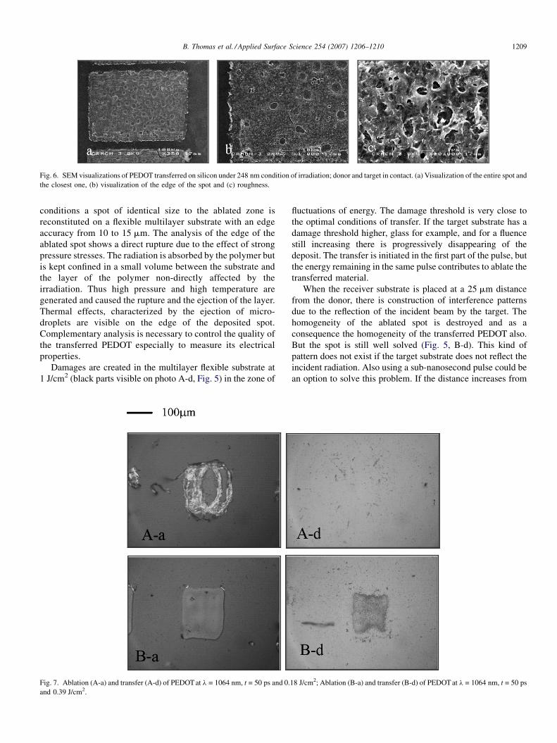
Fig. 6. SEM visualizations of PEDOT transferred on silicon under 248 nm condition of irradiation; donor and target in contact. (a) Visualization of the entire spot and
the closest one, (b) visualization of the edge of the spot and (c) roughness.
B. Thomas et al. / Applied Surface Science 254 (2007) 1206–1210 1209
conditions a spot of identical size to the ablated zone is
reconstituted on a flexible multilayer substrate with an edge
accuracy from 10 to 15 mm. The analysis of the edge of the
ablated spot shows a direct rupture due to the effect of strong
pressure stresses. The radiation is absorbed by the polymer but
is kept confined in a small volume between the substrate and
the layer of the polymer non-directly affected by the
irradiation. Thus high pressure and high temperature are
generated and caused the rupture and the ejection of the layer.
Thermal effects, characterized by the ejection of micro-
droplets are visible on the edge of the deposited spot.
Complementary analysis is necessary to control the quality of
the transferred PEDOT especially to measure its electrical
properties.
Damages are created in the multilayer flexible substrate at
1 J/cm2 (black parts visible on photo A-d, Fig. 5) in the zone of
Fig. 7. Ablation (A-a) and transfer (A-d) of PEDOT at l = 1064 nm, t = 50 ps and 0.
and 0.39 J/cm2.
fluctuations of energy. The damage threshold is very close to
the optimal conditions of transfer. If the target substrate has a
damage threshold higher, glass for example, and for a fluence
still increasing there is progressively disappearing of the
deposit. The transfer is initiated in the first part of the pulse, but
the energy remaining in the same pulse contributes to ablate the
transferred material.
When the receiver substrate is placed at a 25 mm distance
from the donor, there is construction of interference patterns
due to the reflection of the incident beam by the target. The
homogeneity of the ablated spot is destroyed and as a
consequence the homogeneity of the transferred PEDOT also.
But the spot is still well solved (Fig. 5, B-d). This kind of
pattern does not exist if the target substrate does not reflect the
incident radiation. Also using a sub-nanosecond pulse could be
an option to solve this problem. If the distance increases from
18 J/cm2; Ablation (B-a) and transfer (B-d) of PEDOT at l = 1064 nm, t = 50 ps
B. Thomas et al. / Applied Surface Science 254 (2007) 1206–12101210
25 to 50 mm or more it is impossible to keep a good shape of the
transferred PEDOT.
The third condition of absorption experimented is 248 nm.
This radiation is strongly absorbed by the polymer but we have
to keep in mind that UV radiation destroyed the electrical
properties of the PEDOT. It was still interesting to work with
this radiation to study if the ablation and transfer occurs in a
different ways. We can presume in a first approach that the
conductivity will be only modified in the first nanometers of the
layer directly photo-ablated. Complementary electrical mea-
surements will be done on the deposited PEDOT. The ejection
of the polymer as a solid ‘‘confetti’’ occurs at a low fluence
(0.12 J/cm2), but a uniform and homogenous deposit is obtain
in a very small range of fluence. SEM visualizations of the
transferred PEDOT on silicon in such conditions are reported in
Fig. 6. The edge of the deposit is well solved and shows a
rupture under mechanical stresses (Fig. 6b). There is no
droplets ejection due to thermal effects that can be seen outside
the transferred PEDOT. A clean channel is obtained between
two spots. In this case the size of the transfer spot is
150 mm � 220 mm and the size of the channel is 20 mm. A
channel length around 10 mm can be easily obtain with the
same conditions. A high roughness (Fig. 6c) is visible at the
surface of the transferred PEDOT.
3.2. Influence of the pulse duration
Some results obtained in nanosecond regime show the
possible interest to use shorter pulses with the objective of
reducing the heating effects or working in a larger range of
fluence. The experiments undertaken with a pico-second laser
and a femto-second laser show similar results.
At 1064 nm the beam is absorbed by the polymer. At a low
fluence the film of PEDOT is separated from the substrate and
starts to lose its cohesion. The absorption of the beam occurs in
the PEDOT, at the interface with the substrate. It remains
confined by the not irradiated PEDOT layer. A kind of bubble
containing the products of the interaction is formed and begins
to expand (Fig. 7-a and -d). In this case, the pressure stresses
induced during the pulse are not high enough to break
completely the film of polymer. At the opposite of the
nanosecond regime the absorption of the radiation is very
uniform on all the spot. The all ablation of the film is obtained
for 0.4 J/cm2. Only a part of the film is transferred and forms a
homogenous deposit with a very small thickness. The shape of
the transferred part is difficult to control and varies from one
shot to another. Another part of the film is ejected as micro-
fragments.
4. Conclusion
Experiments have been carried out on the LIFT of 300 nm
PEDOT coatings under different conditions of irradiation and
laser pulse duration. Interesting results have been obtained in
nanosecond regime especially when the PEDOT is very
absorbing to the incident radiation (248 nm). The film keeps its
cohesion during the transfer and a precise cutting of the edge is
obtained. Moreover, the transfer occurs at very low fluence
conditions, under the damage threshold of the multilayer
flexible substrate.
The results obtained in the shorter pulse regimes show a
difficulty to control the transfer. But if this transfer is partial the
first electrical measurements, show that the transferred film has
electrical conducting properties.
Another interesting way to trap the incident energy is to use
a transition-absorbing layer in order to avoid the thermal effects
and the direct irradiation of the polymer layer.
Acknowledgments
This work is performed with a financial support obtained
trough the MICROPOLY framework (CIMPACA).
Special acknowledgments to the GCOM2 and the CRMCN
laboratories (Marseille).
References
[1] D.B. Chrisey, A. Pique, J. Fitz-Gerald, R.C.Y. Auyeung, R.A. McGill, H.D.
Wu, M. Duignan, Appl. Surf. Sci 154–155 (2000) 593.
[2] A. Pique, D.B. Chrisey, R.C.Y. Auyeung, J. Fitz-Gerald, H.D. Wu, R.A.
McGill, S. Lakeou, P.K. Wu, V. Nguyen, M. Duignan, Appl. Phys. A 69
(Suppl.) (1999) S279.
[3] L. Landstrom, J. Klimstein, G. Schrems, K. Piglmayer, D. Bauerle, Appl.
Phys. A 78 (2004) 537.
[4] I. Zergioti, D.G. Papazouglou, A. Karaistou, N.A. Vainos, C. Fotakis, Appl.
Surf. Sci. 197–198 (2002) 868.
[5] I. Zergioti, A. Karaiskou, D.G. Papazoglou, C. Fotakis, M. Kapsetaki, D.
Kafetzopoulos, Appl. Surf. Sci. 247 (2005) 584.
[6] Z.H. Kafafi, P.A. Lane (Eds.), Organic Light Emitting Materials and
Devices VIII, vol. 5519, SPIE, 2004, p. 12.
[7] D.B. Chrisey, A. Pique, R.A. McGill, J.S. Horwitz, B.R. Ringeisen, Chem.
Rev. 103 (2003) 553.