experimental realization of deep-subwavelength...
TRANSCRIPT
SC I ENCE ADVANCES | R E S EARCH ART I C L E
PHYS I CS
1Department of Physics and Astronomy, Vanderbilt University, Nashville, TN37235, USA. 2IBM Thomas J. Watson Research Center, 1101 Kitchawan Road, York-town Heights, NY 10598, USA. 3Laboratoire de Nanotechnologie et d’InstrumentationOptique, Institut Charles Delaunay CNRS-UMR 6281, Université de Technologie deTroyes, Troyes 10004, France. 4Department of Electrical Engineering and ComputerScience, Vanderbilt University, Nashville, TN 37235, USA.*Corresponding author. Email: [email protected] (S.H.); [email protected] (S.M.W.)
Hu et al., Sci. Adv. 2018;4 : eaat2355 24 August 2018
Copyright © 2018
The Authors, some
rights reserved;
exclusive licensee
American Association
for the Advancement
of Science. No claim to
originalU.S. Government
Works. Distributed
under a Creative
Commons Attribution
NonCommercial
License 4.0 (CC BY-NC).
Experimental realization of deep-subwavelengthconfinement in dielectric optical resonatorsShuren Hu1*, Marwan Khater2, Rafael Salas-Montiel3, Ernst Kratschmer2, Sebastian Engelmann2,William M. J. Green2, Sharon M. Weiss1,4*
The ability to highly localize light with strong electric field enhancement is critical for enabling higher-efficiencysolar cells, light sources, andmodulators. While deep-subwavelengthmodes can be realized with plasmonic resonators,large losses in these metal structures preclude most practical applications. We developed an alternative approach toachieving subwavelength localization of the electric anddisplacement fields that is not accompaniedby inhibitive losses.We experimentally demonstrate a dielectric bowtie photonic crystal structure that supports mode volumes com-mensurate with plasmonic elements and quality factors that reveal ultralow losses. Our approach opens the door tothe extremely strong light-matter interaction regime with, simultaneously incorporating both an ultralow mode vol-ume and an ultrahigh quality factor, that had remained elusive in optical resonators.
Do
on Septem
ber 15, 2018http://advances.sciencem
ag.org/w
nloaded from
INTRODUCTIONLight-matter interaction in an optical resonator is enhanced throughtwo confinement mechanisms: (i) temporal confinement, which is thephoton cavity lifetime and is characterized by the quality factor (Q), and(ii) spatial confinement, which is the ability to localize light into a tightlyconfined space and is characterized by the modal volume (Vm). Here,the traditional definition of mode volume (Vm) is considered usingEq. 1 (where E is the electric field and e is the permittivity), which ismost strongly scaled by peak electric field energy and ismost relevantfor applications relying on Purcell enhancement and strongly enhancednonlinear optical processes
Vm ¼ ∫eE2dV
maxðeE2Þ ð1Þ
Simultaneously achieving high confinement in both categorieshas been a long-time pursuit in nanophotonics research and holdsthe promise for revolutionary advances in generating, modulating,and detecting light, including higher-efficiency light sources (1–4)and solar cells (5–8), as well as faster and lower power consumptionoptical switches and modulators (9–13). Plasmonic and metal-basedmetamaterial structures are capable of concentrating light into deep-subwavelength volumes [that is, mode volume =Vm~ 10−3 (l/nair)
3] byaccessing a surface plasmon resonance (6, 14, 15). However, resistiveheating losses lead to poor temporal confinement (that is, qualityfactor = Q ~ 10) and prohibit the realization of practical devices thatrequire propagation of energy (16). Recent work replacing metals withall-dielectric materials has led to encouraging progress for enhancedspatial light localization through scattering in high-index dielectricnanoparticles, but the lack of an intrinsic confinement mechanismwithin these dielectric structures has prevented light concentration onpar with plasmonics. Furthermore, the scattering mechanism in these
subwavelength dielectric nanoparticles is incapable of providing tem-poral confinement (17–19).
Historically, low-loss dielectric structures, such as interferometersand ring resonators, have been the building blocks of photonic tech-nologies, but they are diffraction-limited and are therefore unable tofocus light below l/2nd, where nd is the refractive index of the dielectricmaterial in which the optical mode is confined. Photonic crystals haveprovided the best confinement in lossless dielectric materials to date(20). Typical photonic crystals use a simple unit cell geometry—circlesor rectangles (21–23)—and have a Vm ~ 1 (l/nd)
3. Slotted photoniccrystal cavities can further squeeze light into a nanoscale low-indexregionby designing an abrupt index discontinuity along the electric fieldpolarization direction. Slotted photonic crystal cavities reduce theVm to~0.01 (l/nair)
3, almost two orders of magnitude lower than traditionalphotonic crystal cavities (24, 25). However, it is difficult to achieve deepersubwavelength confinement via a slot configuration alone. In addition,because slotted photonic structures inherently confine cavitymodeswith-in a low-index region, they are not suitable for applications requiringstrong light-matter interaction in high-index materials, such as siliconor many highly nonlinear optical materials.
While spatial localization of photons typically occurs due to a singlephysical mechanism, such as total internal reflection in waveguides andphotonic bandgap confinement in photonic crystals, it is apparentfrom previous work that a second level of spatial localization is possi-ble (6, 15, 24–26). In the case of slotted photonic crystal waveguides,light is first confined in the dielectric mode by the photonic bandgapeffect such that light is spatially localized in the dielectric region be-tween the lattice holes. Then, introduction of an air slot that cutsthrough the dielectric region further localizes the light within thisair slot due to electromagnetic boundary conditions. Our previouslyreported theoretical study suggests that this two-step light confine-ment effect can be best exploited to achieve lowmode volume by usingsubwavelength modifications of the photonic crystal lattice holes ratherthan the dielectric region between lattice holes (26). In that study, light isfirst confined in the air mode by the photonic bandgap effect such thatlight is spatially localized inside the lattice air holes. Then, a bowtie-shaped subwavelength dielectric inclusion added to the lattice holesenables redistribution of the optical mode to the tips of the bowtie asa result of electromagnetic boundary conditions. The two-step light lo-calization process in photonic crystals preserves the high-Q nature ofthe photonic crystal cavity. A later theoretical study also found that a
1 of 6

SC I ENCE ADVANCES | R E S EARCH ART I C L E
bowtie-shaped subwavelength dielectric inclusion in the center of aslotted photonic crystal nanobeam with a 1-nm air gap between thebowtie tips enables extremely high Q/Vm values (27). Here, we intro-duce design improvements to bowtie-shaped photonic crystal unit cellsthat enable additional mode confinement in the out-of-plane directionaccompanied by a commensurate increase in the peak electric fieldstrength, and we experimentally demonstrate a bowtie photonic crystalcavity with a loaded Q factor on the order of 105 and record deep-subwavelength mode confinement in silicon [Vm ~ 10−3 (l/nSi)
3]that is verified by optical near-field measurements. This extremelight concentration is on par with plasmonic resonators, yet the low-lossdielectric material allows a concurrent ultrahigh Q factor (26).
http://advances.scienceD
ownloaded from
RESULTSBowtie photonic crystal cavity designTo achieve improved out-of-plane modal confinement in the bowtieunit cell compared to our previous design of a bowtie photonic crystal,a thickness modulation is added in the bowtie tip region to form av-groove cross-sectional profile that is experimentally realizable.Figure 1 compares the energy distribution in the v-groove bowtie unitcell to a traditional circular unit cell with and without an air slot. Theextreme light localization at the bowtie tips leads to an 80-fold increasein the peak electric field amplitude compared to the circular unit celland an eightfold increase compared to the slotted unit cell.
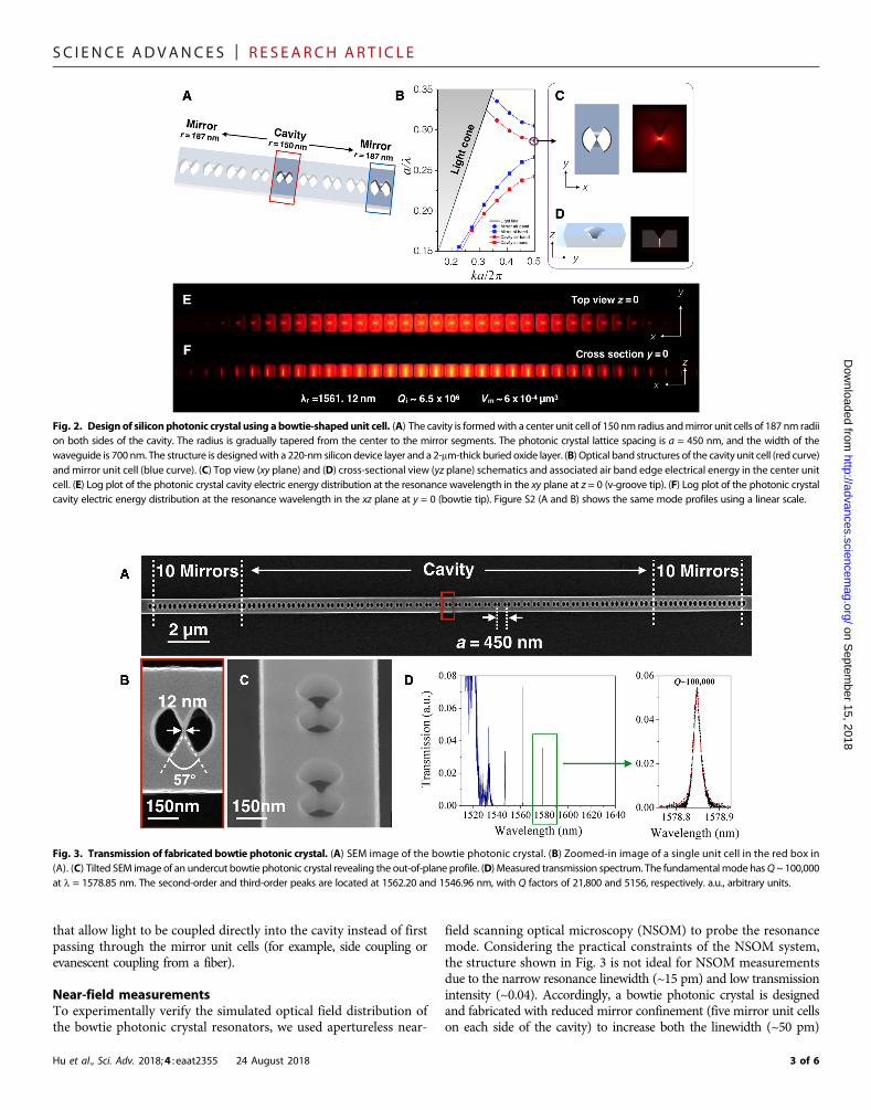
A silicon photonic crystal cavity is designed using the bowtie-shapedunit cell with the v-groove by slowly varying the radius of the unit cell,as shown in Fig. 2A. Because the dielectric bowtie element is inside theenvelope of a traditional air hole, the photonic crystal is designed toconfine the air mode such that light is localized into the air hole region
Hu et al., Sci. Adv. 2018;4 : eaat2355 24 August 2018
on Septem
ber 15, 2018m
ag.org/
and then further localized to the tips of the dielectric bowtie within theair hole region. The band diagram in Fig. 2B shows that the air modeof the bowtie photonic crystal cavity unit cell lies within the modegap of the mirror unit cells, providing the requisite confinementfor the cavity mode. The wavelength of the cavity air mode is ap-proximately 1570 nm at the band edge [kx = 0.5(2p/a)]. As is the casefor all one-dimensional (1D) photonic crystal cavities, theQ factor ofthe bowtie photonic crystal cavity is governed in large part by theband gap tapering from the cavity to mirror unit cells. We choose totransition between the center and mirror unit cells in a quadratic fash-ion, similar to the approach followed in other high-Q photonic crystaldesigns (21–23).
Figure 2 (C and D) shows the top and side view profiles of theoptical mode in the center cavity unit cell, and the electric energy(proportional to ɛE2) across the bowtie photonic crystal cavity is shownin Fig. 2 (E and F) and fig. S2 (A and B). We note that, because thedimensions of the bowtie photonic crystal are the same for allsimulations, the electric energy is directly proportional to electricenergy density. In this simulation, there are 20 tapering unit cellsbetween the central cavity unit cell and the 10 mirror unit cells oneach side of the cavity; not all unit cells are shown in the figures.The mode is highly confined between the bowtie tips in the centralcavity unit cell (fig. S2, C and D) and decays gradually into the mirrorsegments, giving a Gaussian-shaped electric energy profile that mini-mizes radiation losses (fig. S2E). At the resonance wavelength of l =1561.12 nm, the simulated Q factor is 6.55 × 10⁶. The Vm is calculatedto be 6.09 × 10⁻⁴ mm3 using Eq. 1. Given the small dimensions of thebowtie tip, the mode extends partially in air and partially in silicon.Hence, the normalized mode volume should fall between that of themode volume normalized to the wavelength in silicon [Vm = 6.7 ×10⁻³ (l/nSi)
3] and the mode volume normalized to the wavelength inair [Vm = 1.6 × 10⁻⁴ (l/nair)
3]. This mode volume is about two ordersof magnitude smaller than those of other photonic crystal cavities, asshown in table S1 (22–24, 28, 29).
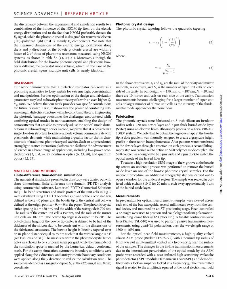
Fabricated bowtie photonic crystal cavity and measuredQ factorFigure 3A shows a scanning electronic microscope (SEM) image ofthe fabricated bowtie photonic crystal with 20 tapering unit cellsand 10 mirror unit cells on each side of the central cavity unit cell.The width of the bowtie tip connection is estimated to be approximately12 nm (Fig. 3B). Given that there are only a few pixels comprisingthe bowtie tip, this value has a relatively large error bar of ±5 nm.The bowtie angle is estimated to be approximately 57°. The radii ofcenter and mirror unit cells are measured to be 147 and 190 nm,respectively. The width of waveguide is measured to be 691 nm.Figure 3C shows a titled SEM image that reveals the v-shaped struc-ture at the bowtie tip; the unit cells shown in this image are from aphotonic crystal fabricated by the same process as the one in Fig. 3Abut released from the oxide substrate using a buffered hydrofluoricacid etch. Transmission measurements carried out on the bowtie pho-tonic crystal show that the fundamental mode at lr = 1578.85 nmhas a loaded Q of approximately 1 × 10⁵ (Fig. 3D). The modessupported by the photonic crystal are located near the short wavelengthband edge (~1520 nm), which is consistent with design (Figs. 2B and3D). The transmission intensity of the resonance peaks is low com-pared to that of the band edge (fig. S3) due to the high mirror con-finement in the cavity. We anticipate that higher Q resonances canbe designed and measured by using alternate coupling techniques
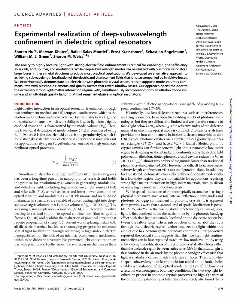
Fig. 1. Comparison of light concentration in different photonic crystal unit cells.(A and B) Traditional circular unit cell of a photonic crystal and its electric energyprofile at the dielectric mode band edge. (C and D) Slotted photonic crystal unitcell and its electric energy profile at the dielectric band edge. (E and F) Bowtiephotonic crystal unit cell and its electric energy profile at the air band edge. Thetip of the v-groove is modeled to extend down to the middle of the silicon slab.(G) 3D profile of the mode in the bowtie unit cell showing the electric energydistribution. All profiles are taken at the middle of the silicon slab. All color mapsare scaled according to the minimum and maximum electrical energy values ofeach individual unit cell. The maximum electric field amplitude in each unit cellscales as follows: traditional circular unit cell = 1 (normalized), slotted unit cell = 10,bowtie unit cell = 80.
2 of 6
SC I ENCE ADVANCES | R E S EARCH ART I C L E
on Septem
ber 15, 2018http://advances.sciencem
ag.org/D
ownloaded from
that allow light to be coupled directly into the cavity instead of firstpassing through the mirror unit cells (for example, side coupling orevanescent coupling from a fiber).
Near-field measurementsTo experimentally verify the simulated optical field distribution ofthe bowtie photonic crystal resonators, we used apertureless near-
Hu et al., Sci. Adv. 2018;4 : eaat2355 24 August 2018
field scanning optical microscopy (NSOM) to probe the resonancemode. Considering the practical constraints of the NSOM system,the structure shown in Fig. 3 is not ideal for NSOM measurementsdue to the narrow resonance linewidth (~15 pm) and low transmissionintensity (~0.04). Accordingly, a bowtie photonic crystal is designedand fabricated with reduced mirror confinement (five mirror unit cellson each side of the cavity) to increase both the linewidth (~50 pm)
Fig. 2. Design of siliconphotonic crystal using a bowtie-shaped unit cell. (A) The cavity is formedwith a center unit cell of 150 nm radius andmirror unit cells of 187 nm radiion both sides of the cavity. The radius is gradually tapered from the center to the mirror segments. The photonic crystal lattice spacing is a = 450 nm, and the width of thewaveguide is 700 nm. The structure is designedwith a 220-nm silicon device layer and a 2-mm-thick buried oxide layer. (B) Optical band structures of the cavity unit cell (red curve)andmirror unit cell (blue curve). (C) Top view (xy plane) and (D) cross-sectional view (yz plane) schematics and associated air band edge electrical energy in the center unitcell. (E) Log plot of the photonic crystal cavity electric energy distribution at the resonance wavelength in the xy plane at z = 0 (v-groove tip). (F) Log plot of the photonic crystalcavity electric energy distribution at the resonance wavelength in the xz plane at y = 0 (bowtie tip). Figure S2 (A and B) shows the same mode profiles using a linear scale.
Fig. 3. Transmission of fabricated bowtie photonic crystal. (A) SEM image of the bowtie photonic crystal. (B) Zoomed-in image of a single unit cell in the red box in(A). (C) Tilted SEM image of an undercut bowtie photonic crystal revealing the out-of-plane profile. (D) Measured transmission spectrum. The fundamental mode hasQ~ 100,000at l = 1578.85 nm. The second-order and third-order peaks are located at 1562.20 and 1546.96 nm, with Q factors of 21,800 and 5156, respectively. a.u., arbitrary units.
3 of 6

SC I ENCE ADVANCES | R E S EARCH ART I C L E
Dow
nloaded
and transmission intensity (~0.2), as shown in fig. S4. Because themode is tightly confined in the cavity, the mode volume is not changedby reducing the number of mirror unit cells (Vm = 6.09 × 10⁻⁴ mm3
for five mirror unit cells). Consequently, conclusions drawn fromNSOM measurements on the five-mirror unit cell bowtie photoniccrystal are also applicable to the higher Q cavities with additionalmirror unit cells. The NSOM operates in a tapping mode in whichthe tip oscillates from 0 to 30 nm above the sample surface. There-fore, the near field measured by the NSOM does not directly cor-respond to the calculated mode volume within the bowtie (Fig. 2E).To correlate experiment and simulation, we simulate the electricenergy localization in the central unit cell of bowtie photonic crystalat 15 nm above the silicon surface as an estimate of the expected av-erage scattering field that can be detected by the NSOM (Fig. 4A). Thecalculated size of the electric energy localization, which is esti-mated by the full width at half maximum (FWHM) of the electricenergy distribution in the unit cell, linearly increases from thecenter of the silicon slab (fig. S5) and is estimated to be ~183 nmalong the y direction and 143 nm along the x direction at a distanceof 15 nm above the silicon surface. Figure 4 (B and C) shows theatomic force microscope (AFM) topology and simultaneously
Hu et al., Sci. Adv. 2018;4 : eaat2355 24 August 2018
measured optical near-field mapping of the bowtie photonic crystalcavity, respectively. The shape of the bowties shown in Fig. 4B isdistorted due to the resolution limit of the AFM mode of the NSOMwhen measuring bowtie features that reside below the surface of thesample using a tapping mode above the surface of the sample. TheSEM image shown in the inset of Fig. 4B reveals the actual shape ofone of the bowtie unit cells in this sample. The measured electricenergy (Fig. 4C) is confined at the bowtie tips, in agreement withthe simulated electric energy (Fig. 4A) distribution in the cavity.Figure 4 (D and E) shows the measured electric energy profilesalong x and y slices of the central unit cell. We identify the siliconregion as the shaded area in Fig. 4 (D and E), based on AFM mea-surements (Fig. 4, D and E, dotted line). The simulated electricenergy profiles are shown by the blue curves in Fig. 4 (D and E).The NSOM-measured profile (red markers) along the y slice throughthe center of the cavity shows a sharp tip of the field at the bowtiecenter, indicating a concentrated electric energy. The size is estimatedto be ~175 nm by considering the FWHM of the electric energydistribution in the central cavity unit cell, which is in agreement withsimulation. The NSOM-measured field profile along the x slicethrough the center of the cavity has an FWHM of ~267 nm.We attribute
on Septem
ber 15, 2018http://advances.sciencem
ag.org/from
Fig. 4. Analysis of spatial confinement via NSOM measurements. (A) Schematic of bowtie photonic crystal cavity with overlay of simulated electric energy 15 nmabove the silicon surface, where the NSOM measures the scattered field. (B) AFM measurement and (C) corresponding electric energy distribution, as measured byNSOM. The inset in (B) shows a higher-resolution SEM image of one of the bowtie unit cells from the measured cavity. (D and E) Simulated and NSOM-measured near-field profile along the y direction and x direction, respectively, along with superimposed AFM line scan.
4 of 6
SC I ENCE ADVANCES | R E S EARCH ART I C L E
the discrepancy between the experimental and simulation results to acombination of the influence of the NSOM tip itself on the electricenergy distribution and to the fact that NSOM preferably detects theEz signal, while the photonic crystal is designed for transverse electric(TE)–polarized light (that is, mainly Ey component). We note thatthe measured dimensions of the electric energy localization alongthe x and y directions of the bowtie photonic crystal are within afactor of 2 of those of plasmonic resonators measured using NSOMsystems, as shown in table S2 (14, 30, 31). Moreover, although thefield distribution for the bowtie photonic crystal and plasmonic bow-ties is different, the calculated mode volume, which, in the case of thephotonic crystal, spans multiple unit cells, is nearly identical.
http://advances.sciencemag.org/
Dow
nloaded from
DISCUSSIONOur work demonstrates that a dielectric resonator can serve as apromising alternative to lossy metals for extreme light concentrationand manipulation. Further optimization of the design and fabricationparametersmay lead to bowtie photonic crystals with an even higherQ/Vm ratio. We believe that our work provides two specific contributionsfor future research. First, it showcases the power of combining sub-wavelength dielectric structure with photonic band theory. Engineeringthe photonic bandgap overcomes the challenges encountered whileconfining optical modes in nanoscatterers, enabling the design ofnanoscatterers that are able to precisely adjust the optical mode distri-butions at subwavelength scales. Second, we prove that it is possible in asingle, low-loss structure to achieve amode volume commensurate withplasmonic elements while maintaining a quality factor that is char-acteristic of traditional photonic crystal cavities. Such an unprecedentedstrong light-matter interaction platform can facilitate the advancementof science in a broad range of applications, including low-power opto-electronics (1, 3, 4, 9–12), nonlinear optics (6, 13, 20), and quantumoptics (32, 33).
on Septem
ber 15, 2018
MATERIALS AND METHODSFinite-difference time-domain simulationsThe numerical simulations presented in this studywere carried out withthree-dimensional finite-difference time-domain (FDTD) analysisusing commercial software, Lumerical FDTD (Lumerical SolutionsInc.). The band structures and mode profiles of the unit cells in Fig. 2were calculated using FDTD. The center xy plane of the silicon slab wasdefined as the z = 0 plane, and the bowtie tip of the central unit cell wasdefined as the origin point x= 0, y= 0 in the paper. The photonic crystallattice spacing is a = 450 nm, and the width of the waveguide is 700 nm.The radius of the center unit cell is 150 nm, and the radii of the mirrorunit cells are 187 nm. The bowtie tip angle is designed to be 60°. Theout-of-plane height of the bowtie tip center is defined to be half of thethickness of the silicon slab to be consistent with the dimensions ofthe fabricated structures. The bowtie height is linearly tapered overan in-plane distance equal to 75 nm such that the vertical angle is 34°(see Figs. 2D and 3C). The mesh size within the photonic crystal latticeholes was chosen to be a uniform 4 nm per grid, while the remainder ofthe simulation space is meshed by the Lumerical default conformalmesh. For the cavity simulation, symmetric boundary conditions wereapplied along the x direction, and antisymmetric boundary conditionswere applied along the y direction to reduce the calculation time. Thesource was defined as amagnetic dipoleHz at the (225 nm, 0 nm, 0 nm)coordinate.
Hu et al., Sci. Adv. 2018;4 : eaat2355 24 August 2018
Photonic crystal designThe photonic crystal tapering follows the quadratic tapering
ri ¼ r0 1þ im
� �2 !
ð2Þ
where
m ¼ Ncffiffiffiffiffiffiffiffiffiffiffiffirmr0� 1
q ð3Þ
In the above expressions, r0 and rm are the radii of the cavity andmirrorunit cells, respectively, and Nc is the number of taper unit cells on eachside of the cavity. In our design, r0 = 150 nm, rm = 187 nm,Nc = 20, andthere are 10 mirror unit cells on each side of the cavity. Transmissionmeasurements become challenging for a larger number of taper unitcells or larger number of mirror unit cells as the intensity of the funda-mental mode approaches the noise floor.
FabricationThe photonic crystals were fabricated on 8-inch silicon-on-insulatorwafers with a 220-nm device layer and 2-mm-thick buried oxide layer(Soitec) using an electron beam lithography process on a Leica VB6-HR100kV system.We note that, to obtain the v-groove shape at the bowtietip, a dose gradient was manually assigned to create a grayscale heightprofile in the electron beam photoresist. After patterns were transferredto the device layer through a reactive ion etch process, a second lithog-raphy stepwas carried out to define an SU8 polymermode coupler. TheSU8 coupler was designed to be 3 mmwide and 2 mm thick tomatch theoptical mode of the lensed fiber tip.
To attain a high-resolution SEM image of the v-groove at the bowtietip center, an undercut process was performed to remove the buriedoxide layer on one of the bowtie photonic crystal samples. For theundercut procedure, an additional lithography step was carried out toopen a window for the undercut region. The sample was soaked in buf-fered oxide etchant (10:1) for 20 min to etch away approximately 1 mmof the buried oxide layer.
MeasurementsIn preparation for optical measurements, samples were cleaved acrosseach end of the bus waveguide, several millimeters away from the cen-tral device, and mounted on an XY positioning stage. Piezo-controlledXYZ stages were used to position and couple light to/from polarization-maintaining lensed fibers (OZOptics Ltd.). A tunable continuous-wavelaser (Santec TSL-510) was used to perform passive transmission mea-surements, using quasi-TE polarization, over the wavelength range of1500 to 1630 nm.
For the optical near-field measurements, a high-quality etchedsilicon AFM probe (Bruker TESPA-V2) with a nominal tip radius of8 nm was put in intermittent contact at a frequency f0 near the surfaceof the samples. The changes in the in-line transmission measurementsdue to the intermittent perturbation of the optical mode by the AFMprobe were recorded with a near-infrared high-sensitivity avalanchephotodetector (APD module Hamamatsu C5460SPL) and demodu-lated with a lock-in amplifier locked at a frequency f0. The transmittedsignal is related to the amplitude squared of the local electric near field
5 of 6
SC I ENCE ADVANCES | R E S EARCH ART I C L E
normalized to the power carried by the optical mode. An optical imageis constructed based on the demodulated in-line transmissionmeasure-ments as the AFM probe raster scans the sample (scan direction isx direction) at an average distance of 15 nm from its surface. A topogra-phy image was recorded simultaneously to the optical near-field image.A tunable continuouswave laser (PhotoneticsTunicsECL1560)was usedto perform the in-line transmission measurements, using quasi-TEpolarization, over the wavelength range of 1500 to 1630 nm.
Dow
nloaded fro
SUPPLEMENTARY MATERIALSSupplementary material for this article is available at http://advances.sciencemag.org/cgi/content/full/4/8/eaat2355/DC1Fig. S1. Design of photonic crystal cavity in an FDTD simulation.Fig. S2. Resonance mode profile.Fig. S3. Broadband transmission spectrum of bowtie photonic crystal cavity shown in Fig. 3D.Fig. S4. SEM image and transmission of the bowtie photonic crystal cavity characterized byNSOM.Fig. S5. Position-dependent electric energy distribution in the central cavity unit cell of thesilicon bowtie photonic crystal.Table S1. Calculated mode volume (Vm) and measured quality factor (Q) of different photoniccrystal (PhC) cavities including the bowtie photonic crystal cavity presented in this work.Table S2. NSOM-measured mode sizes of plasmonic structures in comparison to dielectricbowtie photonic crystal reported in this work.
on Septem
ber 15, 2018http://advances.sciencem
ag.org/m
REFERENCES AND NOTES1. S. Noda, M. Fujita, T. Asano, Spontaneous-emission control by photonic crystals and
nanocavities. Nat. Photonics 1, 449–458 (2007).2. R. F. Oulton, V. J. Sorger, T. Zentgraf, R.-M. Ma, C. Gladden, L. Dai, G. Bartal, X. Zhang,
Plasmon lasers at deep subwavelength scale. Nature 461, 629–632 (2009).3. H. Altug, D. Englund, J. Vučković, Ultrafast photonic crystal nanocavity laser. Nat. Phys. 2,
484–488 (2006).4. S. Matsuo, A. Shinya, T. Kakitsuka, K. Nozaki, T. Segawa, T. Sato, Y. Kawaguchi, M. Notomi,
High-speed ultracompact buried heterostructure photonic-crystal laser with 13 fJ ofenergy consumed per bit transmitted. Nat. Photonics 4, 648–654 (2010).
5. H. A. Atwater, A. Polman, Plasmonics for improved photovoltaic devices. Nat. Mater. 9,205–213 (2010).
6. J. A. Schuller, E. S. Barnard, W. Cai, Y. Chul Jun, J. S. White, M. L. Brongersma,Plasmonics for extreme light concentration and manipulation. Nat. Mater. 9, 193–204(2010).
7. M. A. Green, S. Pillai, Harnessing plasmonics for solar cells. Nat. Photonics 6, 130–132(2012).
8. M. L. Brongersma, Y. Cui, S. H. Fan, Light management for photovoltaics using high-indexnanostructures. Nat. Mater. 13, 451–460 (2014).
9. G. T. Reed, G. Mashanovich, F. Y. Gardes, D. J. Thomson, Silicon optical modulators.Nat. Photonics 4, 518–526 (2010).
10. Q. Xu, B. Schmidt, S. Pradhan, M. Lipson, Micrometre-scale silicon electro-opticmodulator. Nature 435, 325–327 (2005).
11. J. C. Rosenberg, W. M. Green, S. Assefa, D. M. Gill, T. Barwicz, M. Yang, S. M. Shank,Y. A. Vlasov, A 25 Gbps silicon microring modulator based on an interleaved junction.Opt. Express 20, 26411–26423 (2012).
12. A. Melikyan, L. Alloatti, A. Muslija, D. Hillerkuss, P. C. Schindler, J. Li, R. Palmer, D. Korn,S. Muehlbrandt, D. Van Thourhout, B. Chen, R. Dinu, M. Sommer, C. Koos, M. Kohl,W. Freude, J. Leuthold, High-speed plasmonic phase modulators. Nat. Photonics 8,229–233 (2014).
13. K. Nozaki, T. Tanabe, A. Shinya, S. Matsuo, T. Sato, H. Taniyama, M. Notomi,Sub-femtojoule all-optical switching using a photonic-crystal nanocavity. Nat. Photonics4, 477–483 (2010).
14. Y. Luo, M. Chamanzar, A. Apuzzo, R. Salas-Montiel, K. N. Nguyen, S. Blaize, A. Adibi,On-chip hybrid photonic–plasmonic light concentrator for nanofocusing in an integratedsilicon photonics platform. Nano Lett. 15, 849–856 (2015).
15. M.-K. Kim, H. Sim, S. Ju Yoon, S.-H. Gong, C. Won Ahn, Y.-H. Cho, Y.-H. Lee, Squeezingphotons into a point-like space. Nano Lett. 15, 4102–4107 (2015).
16. J. C. Ndukaife, V. M. Shalaev, A. Boltasseva, Plasmonics—Turning loss into gain. Science351, 334–335 (2016).
17. J. Yan, P. Liu, Z. Lin, H. Wang, H. Chen, C. Wang, G. Yang, Directional Fano resonance in asilicon nanosphere dimer. ACS Nano 9, 2968–2980 (2015).
Hu et al., Sci. Adv. 2018;4 : eaat2355 24 August 2018
18. R. M. Bakker, D. Permyakov, Y. Feng Yu, D. Markovich, R. Paniagua-Domínguez,L. Gonzaga, A. Samusev, Y. Kivshar, B. Luk’yanchuk, A. I. Kuznetsov, Magnetic and electrichotspots with silicon nanodimers. Nano Lett. 15, 2137–2142 (2015).
19. R. Regmi, J. Berthelot, P. M. Winkler, M. Mivelle, J. Proust, F. Bedu, I. Ozerov, T. Begou,J. Lumeau, H. Rigneault, M. F. García-Parajó, S. Bidault, J. Wenger, N. Bonod, All-dielectricsilicon nanogap antennas to enhance the fluorescence of single molecules. Nano Lett.16, 5143–5151 (2016).
20. A. F. Koenderink, A. Alù, A. Polman, Nanophotonics: Shrinking light-based technology.Science 348, 516–521 (2015).
21. E. Kuramochi, H. Taniyama, T. Tanabe, K. Kawasaki, Y.-G. Roh, M. Notomi, Ultrahigh-Qone-dimensional photonic crystal nanocavities with modulated mode-gap barriers onSiO2 claddings and on air claddings. Opt. Express 18, 15859–15869 (2010).
22. Q. Quan, P. B. Deotare, M. Loncar, Photonic crystal nanobeam cavity strongly coupled tothe feeding waveguide. Appl. Phys. Lett. 96, 203102 (2010).
23. Q. Quan, M. Loncar, Deterministic design of wavelength scale, ultra-high Q photoniccrystal nanobeam cavities. Opt. Express 19, 18529–18542 (2011).
24. P. Seidler, K. Lister, U. Drechsler, J. Hofrichter, T. Stöferle, Slotted photonic crystalnanobeam cavity with an ultrahigh quality factor-to-mode volume ratio. Opt. Express 21,32468–32483 (2013).
25. J. D. Ryckman, S. M. Weiss, Low mode volume slotted photonic crystal single nanobeamcavity. Appl. Phys. Lett. 101, 071104 (2012).
26. S. Hu, S. M. Weiss, Design of photonic crystal cavities for extreme light concentration.ACS Photonics 3, 1647–1653 (2016).
27. H. Choi, M. Heuck, D. Englund, Self-similar nanocavity design with ultrasmall modevolume for single-photon nanolinearities. Phys. Rev. Lett. 118, 223605 (2017).
28. Y. Akahane, T. Asano, B.-S. Song, S. Noda, High-Q photonic nanocavity in atwo-dimensional photonic crystal. Nature 425, 944–947 (2003).
29. B.-S. Song, S. Noda, T. Asano, Y. Akahane, Ultra-high-Q photonic double-heterostructurenanocavity. Nat. Mater. 4, 207–210 (2005).
30. A. Apuzzo, M. Février, R. Salas-Montiel, A. Bruyant, A. Chelnokov, G. Lérondel, B. Dagens,S. Blaize, Observation of near-field dipolar interactions involved in a metal nanoparticlechain waveguide. Nano Lett. 13, 1000–1006 (2013).
31. V. A. Zenin, A. Andryieuski, R. Malureanu, I. P. Radko, V. S. Volkov, D. K. Gramotnev,A. V. Lavrinenko, S. I. Bozhevolnyi, Boosting local field enhancement by on-chip nanofocusingand impedance-matched plasmonic antennas. Nano Lett. 15, 8148–8154 (2015).
32. T. G. Tiecke, J. D. Thompson, N. P. de Leon, L. R. Liu, V. Vuletić, M. D. Lukin, Nanophotonicquantum phase switch with a single atom. Nature 508, 241–244 (2014).
33. A. Sipahigil, R. E. Evans, D. D. Sukachev, M. J. Burek, J. Borregaard, M. K. Bhaskar,C. T. Nguyen, J. L. Pacheco, H. A. Atikian, C. Meuwly, R. M. Camacho, F. Jelezko, E. Bielejec,H. Park, M. Lončar, M. D. Lukin, An integrated diamond nanophotonics platform forquantum optical networks. Science 354, 847–850 (2016).
Acknowledgments: We thank G. Gaur, K. J. Miller, C. Xiong, and J. S. Orcutt for helpfuldiscussions. The photonic crystal bowtie cavities were fabricated in the MicroelectronicsResearch Laboratory (MRL) at the IBM Thomas J. Watson Research Center. We aregrateful to the MRL staff for their contributions to the success of this work. Simulationspresented in this work were conducted in part using the resources of the AdvancedComputing Center for Research and Education at Vanderbilt University (Nashville, TN).Additional computations were carried out with the resources of the HPC Center ofChampagne-Ardenne ROMEO. Equipment and technical support in the Vanderbilt Institutefor Nanoscale Science and Engineering and French regional nanofabrication andnanocharacterization platform (Nano’Mat) were also used for this work. Funding: Thiswork was supported in part by the NSF (ECCS1407777). Author contributions:S.H. conceived the idea. M.K., E.K., and S.E. fabricated the structure. S.H. performed thetransmission experiments and carried out the simulations. R.S.-M. performed theNSOM measurements. W.M.J.G. and S.M.W. advised on the several aspects of theory andexperiments and supervised the overall research effort. S.H. and S.M.W. wrote themanuscript with input from all authors. Competing interests: The authors declarethat they have no competing interests. Data and materials availability: All data neededto evaluate the conclusions in the paper are present in the paper and/or theSupplementary Materials. Additional data related to this paper may be requestedfrom the authors.
Submitted 6 February 2018Accepted 18 July 2018Published 24 August 201810.1126/sciadv.aat2355
Citation: S. Hu, M. Khater, R. Salas-Montiel, E. Kratschmer, S. Engelmann, W. M. J. Green,S. M. Weiss, Experimental realization of deep-subwavelength confinement in dielectricoptical resonators. Sci. Adv. 4, eaat2355 (2018).
6 of 6

Experimental realization of deep-subwavelength confinement in dielectric optical resonators
M. WeissShuren Hu, Marwan Khater, Rafael Salas-Montiel, Ernst Kratschmer, Sebastian Engelmann, William M. J. Green and Sharon
DOI: 10.1126/sciadv.aat2355 (8), eaat2355.4Sci Adv
ARTICLE TOOLS http://advances.sciencemag.org/content/4/8/eaat2355
MATERIALSSUPPLEMENTARY http://advances.sciencemag.org/content/suppl/2018/08/20/4.8.eaat2355.DC1
REFERENCES
http://advances.sciencemag.org/content/4/8/eaat2355#BIBLThis article cites 33 articles, 3 of which you can access for free
PERMISSIONS http://www.sciencemag.org/help/reprints-and-permissions
Terms of ServiceUse of this article is subject to the
registered trademark of AAAS.is aScience Advances Association for the Advancement of Science. No claim to original U.S. Government Works. The title
York Avenue NW, Washington, DC 20005. 2017 © The Authors, some rights reserved; exclusive licensee American (ISSN 2375-2548) is published by the American Association for the Advancement of Science, 1200 NewScience Advances
on Septem
ber 15, 2018http://advances.sciencem
ag.org/D
ownloaded from