experimental study of electrical breakdown in mems devices ... proc 6884.pdf · we present an...
TRANSCRIPT

Experimental study of electrical breakdown in MEMS devices with micrometer scale gaps
P. Carazzetti, Ph. Renaud, H. R. Shea
Copyright 2008 Society of Photo-Optical Instrumentation Engineers. This paper was published in Proceedings of SPIE Volume 6884 and is made available as an electronic reprint (preprint) with permission of SPIE. One print or electronic copy may be made for personal use only. Systematic or multiple reproduction, distribution to multiple locations via electronic or other means, duplication of any material in this paper for a fee or for commercial purposes, or modification of the content of the paper are prohibited.
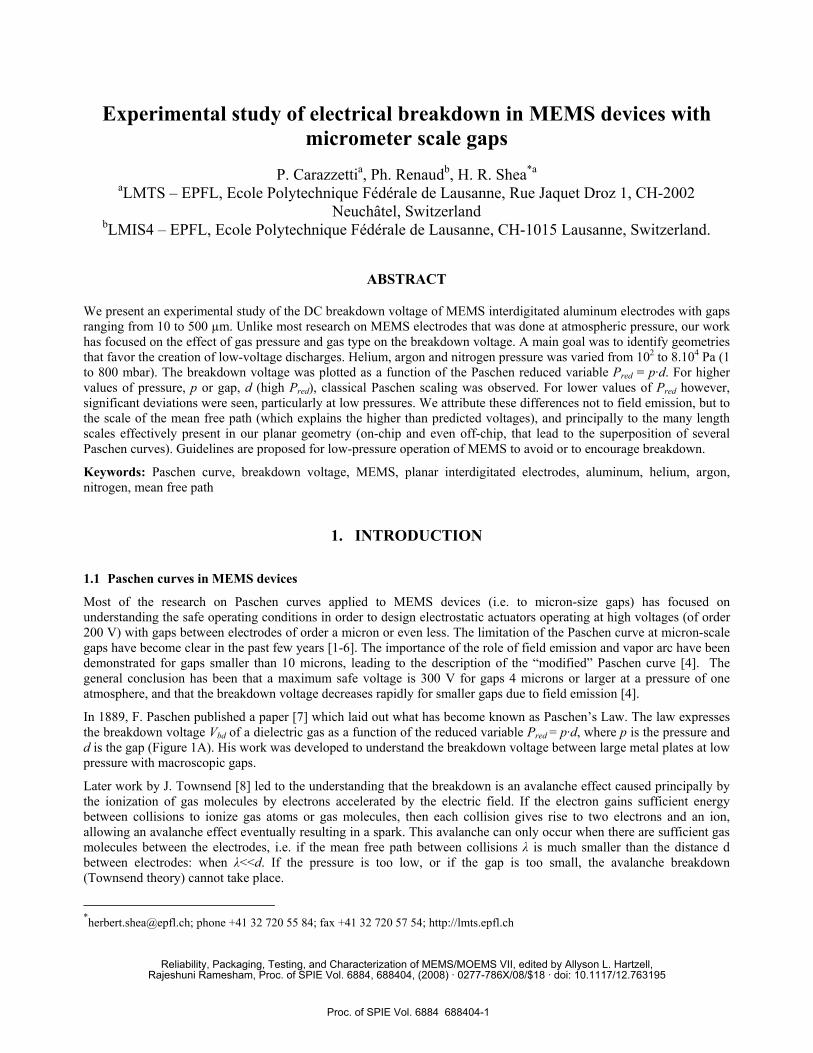
Experimental study of electrical breakdown in MEMS devices with micrometer scale gaps
P. Carazzettia, Ph. Renaudb, H. R. Shea*a
aLMTS – EPFL, Ecole Polytechnique Fédérale de Lausanne, Rue Jaquet Droz 1, CH-2002 Neuchâtel, Switzerland
bLMIS4 – EPFL, Ecole Polytechnique Fédérale de Lausanne, CH-1015 Lausanne, Switzerland.
ABSTRACT
We present an experimental study of the DC breakdown voltage of MEMS interdigitated aluminum electrodes with gaps ranging from 10 to 500 µm. Unlike most research on MEMS electrodes that was done at atmospheric pressure, our work has focused on the effect of gas pressure and gas type on the breakdown voltage. A main goal was to identify geometries that favor the creation of low-voltage discharges. Helium, argon and nitrogen pressure was varied from 102 to 8.104 Pa (1 to 800 mbar). The breakdown voltage was plotted as a function of the Paschen reduced variable Pred = p·d. For higher values of pressure, p or gap, d (high Pred), classical Paschen scaling was observed. For lower values of Pred however, significant deviations were seen, particularly at low pressures. We attribute these differences not to field emission, but to the scale of the mean free path (which explains the higher than predicted voltages), and principally to the many length scales effectively present in our planar geometry (on-chip and even off-chip, that lead to the superposition of several Paschen curves). Guidelines are proposed for low-pressure operation of MEMS to avoid or to encourage breakdown.
Keywords: Paschen curve, breakdown voltage, MEMS, planar interdigitated electrodes, aluminum, helium, argon, nitrogen, mean free path
1. INTRODUCTION 1.1 Paschen curves in MEMS devices
Most of the research on Paschen curves applied to MEMS devices (i.e. to micron-size gaps) has focused on understanding the safe operating conditions in order to design electrostatic actuators operating at high voltages (of order 200 V) with gaps between electrodes of order a micron or even less. The limitation of the Paschen curve at micron-scale gaps have become clear in the past few years [1-6]. The importance of the role of field emission and vapor arc have been demonstrated for gaps smaller than 10 microns, leading to the description of the “modified” Paschen curve [4]. The general conclusion has been that a maximum safe voltage is 300 V for gaps 4 microns or larger at a pressure of one atmosphere, and that the breakdown voltage decreases rapidly for smaller gaps due to field emission [4].
In 1889, F. Paschen published a paper [7] which laid out what has become known as Paschen’s Law. The law expresses the breakdown voltage Vbd of a dielectric gas as a function of the reduced variable Pred = p·d, where p is the pressure and d is the gap (Figure 1A). His work was developed to understand the breakdown voltage between large metal plates at low pressure with macroscopic gaps.
Later work by J. Townsend [8] led to the understanding that the breakdown is an avalanche effect caused principally by the ionization of gas molecules by electrons accelerated by the electric field. If the electron gains sufficient energy between collisions to ionize gas atoms or gas molecules, then each collision gives rise to two electrons and an ion, allowing an avalanche effect eventually resulting in a spark. This avalanche can only occur when there are sufficient gas molecules between the electrodes, i.e. if the mean free path between collisions λ is much smaller than the distance d between electrodes: when λ<<d. If the pressure is too low, or if the gap is too small, the avalanche breakdown (Townsend theory) cannot take place.
*[email protected]; phone +41 32 720 55 84; fax +41 32 720 57 54; http://lmts.epfl.ch
Reliability, Packaging, Testing, and Characterization of MEMS/MOEMS VII, edited by Allyson L. Hartzell,Rajeshuni Ramesham, Proc. of SPIE Vol. 6884, 688404, (2008) · 0277-786X/08/$18 · doi: 10.1117/12.763195
Proc. of SPIE Vol. 6884 688404-1

This absence of atoms or molecules is what gives the minimum in the Paschen curve. At large gaps or pressures, a linear relation breakdown voltage and electrode gap is found (reflecting the constant breakdown electric field of the gas), while at very small gaps one has a “vacuum isolation”, where there are not enough gas atoms or molecules for the avalanche to occur. Later work led to the understanding that the Paschen curve also depends on secondary electrons emitted from the negative electrode when impacted by the positive ions. These electrons further accelerate the breakdown process. The secondary electron yield, γ depends on the cathode material [9,10]. The Paschen curve can be obtained by computing the voltage required for the process of electron emission and multiplication to become self-sustaining [11]. One obtains:
( ) ⎟⎟⎠
⎞⎜⎜⎝
⎛⎟⎟⎠
⎞⎜⎜⎝
⎛+−⋅⋅
⋅⋅=
γ11lnlnln dpA
dpBVbd (1)
where A and B are properties of the gas, and γ is a property of the electrode material.
The Paschen curves were developed for macroscopic electrodes at operating pressures from a few Pa to one atmosphere. The generality of the scaling of Vbd with Pred led researchers to apply it to MEMS devices operating in a variety of gases at one atmosphere, for which a minimum breakdown voltage of order 380 V is predicted at a spacing of 8 microns (the exact numbers depend on the gas).
As reported in [1,2,5,6], when the gaps are less than 10 microns for micromachined structures operated at one atmosphere (Pred < 1 Pa·m), important deviations are seen from the Paschen curve. This regime is one where the mean free path is of order the gap, and thus where the Townsend breakdown cannot occur. Other types of breakdown are however possible. As presented for instance in [4] and in [6], field emission can become important at gaps order 5 microns, leading to a “modified” Paschen curve, which agrees with the “standard” Paschen curves at gaps larger than 10 microns (Pred > 1 Pa·m), exhibits a plateau of constant Vbd between 4 and 10 microns, and a linear drop in Vbd at lower gaps (dotted line on Figure 1A).
1000
800
600
400
200
0
Vbd
20151050p.d [Pa.m]
a)1000
800
600
400
200
0
V bd
100x10380604020p [Pa]
50 micron gap 500 micron gap
b)
Fig. 1. A) Paschen curve for argon (solid line) and modified Paschen curve (dotted line) showing the drop in Vbd at low gaps. B) Paschen curve in argon for gaps of 50 µm (dotted line) and 500 µm (solid line): the minimum voltage for breakdown is constant but the pressure at which the minimum in Vbd occurs is gap dependent.
In addition to the nature of the gas (reflected in the constants A and B of equation 1) and the nature of the electrode (in the form of parameter γ), relevant parameters that must be taken into account are the mean free path of gas atoms species, the surface roughness (which has a strong influence on the field emission), work function of the electrode, and the overall geometry of the electrodes, especially for planar geometries as found in MEMS and integrated circuits, which do not match the conditions of uniform electric field for which the Paschen curves were developed.
B A
Proc. of SPIE Vol. 6884 688404-2

1.2 Motivation of the research
With the exception of the work of one group [10,12,13] Paschen curves for micron-scale gaps have been measured at atmospheric pressure [1,4,14,15], typically in air, which is reasonable given that this is the normal operating condition for MEMS devices. Although Baars-Hibbe and coworkers [10] report on measurements down to 10 kPa, their main objective was creating atmospheric plasmas.
Our motivation is to develop a chip-scale hermetically sealed plasma light source, consisting of Al electrodes spaced by 10 to 500 microns sealed in a stack of three anodically-bonded glass wafers. We report on the fabrication process and optical spectra obtained from this light source in [16] for different gases and pressures. Applications for such a light source include optical pumping in chip-scale atomic clocks, leak detection, and outgassing characterization.
To ignite the plasma discharge, a sufficient AC or DC potential (~300 V) must be applied between the electrodes. For lifetime and power consumption reasons, our chip-scale light source is operated as an RF plasma at frequencies near 20 MHz. RF operation minimizes erosion of the cathode (thus increasing lifetime), and can reduce the minimum voltage required for ignition as reported in [13].
The goal of the study reported here was to compare different electrode gap sizes and gap geometries in order to determine the conditions under which a plasma can be ignited with the lowest possible voltage over a wide pressure range (i.e., 102 to 8·104 Pa, or 1 to 800 mbar). RF plasmas are more complex to understand than DC plasma, with additional lengths scales that need to be considered, primarily the fact that the electrons are confined by field oscillations, and the space-charge sheaths at the plasma boundary.
We therefore investigated the DC Paschen curve of the structure described in the following section, varying both the gap (from 10 to 500 µm) and the pressure (102 to 8·104 Pa), for He, Ar and N2 atmospheres. Our samples thus cover a very large range of Pred: more than 4 order of magnitude from Pred = 10-3 Pa·m to 40 Pa·m, covering regimes of small Pred not accessible to devices (regardless of size) operated at atmospheric pressure because of the field emission occurring at small gaps.
Section 2 presents the sample design and fabrication. In section 3 the measurement setup is described, and data is presented on the breakdown voltage as a function of pressure, gas type and gap size. Experimental data is discussed in section 4.
2. SAMPLE DESIGN AND FABRICATION Interdigitated electrodes with 3 pairs of fingers covering two orders of magnitude of gap spacing were designed and fabricated. Figure 2A is a CAD plot showing the device layout in micrometers. Each finger is 2820 µm long and 240 µm wide. Corrugated edges were used to locally enhance the electric field and hence to lower the voltage required for breakdown. The distance separating the tip of opposite protruding patterns, shown by the scale bars in Figure 2B, is referred to, in following text, as the electrode gap spacing, d. Varying only the parameter d, 8 different electrode versions were designed, namely, d = 10, 20, 40, 100, 150, 200, 300 and 500 µm.
Fig. 2. A) CAD layout showing the overall footprint of a device. B) Close-up showing the 20-µm gap separation between opposite protruding patterns. All dimensions are in micrometers.
A B
Proc. of SPIE Vol. 6884 688404-3

Mg 5.OOKX1 I WD= ST EPFL CMI
Key features of the fabrication process are the use of thick Al films deposited on insulating substrates (fused silica) and patterned with a highly anisotropic dry-etching process that avoids mask undercutting thereby preserving the sharpness of corrugated electrode edges.
In a first step, 8 µm of aluminum were sputter deposited from a pure Al target on 100-mm fused silica substrates. The sputtering process was realized at room temperature with a DC power of 2 kW, leading to a deposition rate of 400 nm/min. The equipment used was a Spider-600 from Pfeiffer Vacuum. Next, a 10 µm-thick layer of Clariant’s AZ9260 photoresist was spun and photographically defined into the mask for patterning the electrodes. Al etching was done with an inductively coupled plasma (ICP) process based on a mixed Cl2/BCl3 chemistry on a STS Multiplex ICP etching tool. The Al was etched at a rate of approximately 300 nm/min and the selectivity toward the mask, considering a load of about 80% of the wafer surface, was observed to be close to unity. Figure 3A is an optical micrograph of a fabricated device with an electrode gap of 40 µm, whereas Figure 3B is a SEM close-up of the patterned aluminum electrodes with smooth and vertical walls enabled by the ICP process.
Fig. 3. A) Optical image of a fabricated device with a gap spacing of 40 µm. B) SEM close-up of 8 µm-thick dry-etched Al electrodes with corrugated edges.
3. RESULTS AND DISCUSSION 3.1 Experimental setup
The DC breakdown characterization presented in this study was performed in a small vacuum chamber (volume of 0.7 l) with feedthroughs for electrical connections (MHV), pressure sensors, gas inlet, pumping and venting (see Figure 4A). Prior to each measurement session, the chamber was pumped down to a base pressure of 0.5 Pa, then purged and filled with He, Ar or N2. The microfabricated chips were mounted on a custom PCB with pads for wirebonds and interface to electrical contacts from the MHV feedthrough, as shown in Figure 4B and Figure 4C, respectively.
Breakdown tests were performed by measuring the current vs. voltage (I-V) characteristic of the device under test (DUT). Voltage was applied across each terminal of the DUT with a high voltage power supply (PS350 from Stanford Research Systems, Inc.) controlled by a LabView program. The voltage was increased in steps of 1 V every 500 ms from an initial value of 50 V until the current increased sharply and exceeded a preset threshold value. The voltage corresponding to the sharp current rise was taken as the breakdown potential, Vbd [4,5]. Depending on the pressure and electrode gap, the sharp rise in current was accompanied by a visible breakdown event, ranging from a weak glow covering the whole device footprint to a localized spark or glow. The compliance current was set at a sufficiently low threshold (0.05 mA) to avoid rapid destruction of the electrodes due to arcing. Paschen curves were thus plotted based on the recorded values of breakdown voltage, Vbd vs. p·d for pressure ranging from 102 to 8·104 Pa.
A B
1 mm
Proc. of SPIE Vol. 6884 688404-4

El iIlTi
Fig. 4. A) Vacuum chamber used for the breakdown measurements, B) device under test (DUT): the microfabricated chip mounted on the PCB, and C) electrical contacts on the PCB.
3.2 Effect of the gas type
To introduce our Paschen curve data, it is helpful to start with an overview of the different types of behavior that were observed. Figure 5 is a plot of breakdown voltage, Vbd vs. pressure, p for three samples with an identical 100-µm gap, in N2, Ar and He. For each pressure, the measurement was repeated five times. Solid symbols on the curves in Figure 5 represent the average of these measurements, whereas the error bars indicate lowest and highest values of the breakdown voltage.
150
200
250
300
350
400
450
500
0 5000 1 104 1.5 104 2 104 2.5 104 3 104
N2
Ar
He
V bd
[V]
P [Pa] Fig. 5. Breakdown voltage, Vbd, vs. pressure, p measured in different gas atmospheres (He, Ar, and N2) on 3 devices with
100 µm gap separation.
At first glance, typical Paschen behavior is observed, as in Figure 1, with the minimum voltage for breakdown being lower for He, than for Ar, and for N2 [10,17]. However, a more quantitative comparison of our experimental data with published values is difficult since Vbd strongly depends on the cathode material [9,17,18] and surface roughness [5,18,19] and also if the breakdown is created in DC or RF mode [10,13,20]. It is reported that RF discharges exhibit significantly lower values of Vbd than DC discharges [12]. The overall shape is as expected from the Paschen theory. However, as discussed later in section 3.6, this theory provides a poor fit when applied to the full pressure range, but provides a very good fit for higher p·d values.
A C
B
Proc. of SPIE Vol. 6884 688404-5

One important point to notice is the double dip in the He curve, which is certainly due to the different lengths scales present in the measurement setup. The dip at 3 kPa corresponds to breakdown on the printed circuit board (gaps between wirebonds of order 3.5 mm), while the higher pressure dip (>10 kPa) is due to breakdown on the microfabricated electrodes. This important element will be discussed in more detail in section 3.3. The cross-over from the chip dominated regime to PCB dominated behavior basically depends on electrode spacing and on gas type: it is easily visible in He, less noticeable in Ar and not observable in N2
3.3 Effect of the gap spacing in helium
The cross-over is clearly illustrated in Figure 6, where experimental Vbd vs. p curves are plotted in He for a sample with a 100 µm gap (Figure 6A) and a 500 µm gap (Figure 6B). As illustrated in Figure 1B, the pressure corresponding to the minimum Vbd scales as 1/d in the Paschen model. Both devices exhibit a minimum breakdown voltage of 160-170 V between 2 to 4 kPa due to the the PCB, as discussed in the previous section. In addition, the device with 100 µm gap has a second dip of value 175 V located around 15 kPa, hence for a product p·d of 1.5 Pa·m. Published data for minimum breakdown in He reported Vbd = 240 V for p·d = 5.5 Pa·m [20] and Vbd = 150 V for p·d = 5.33 Pa·m (or 4 torr·cm) [17]. In Figure 7 data of Vbd for electrode gaps from 10 to 500 µm are overlaid, as a function of pressure (Figure 7A) and Pred = p·d (Figure 7B). For clarity, the error bars are no longer displayed. All the samples except the PCB and the chip with larger gap (d = 500 µm), exhibit a dip with minimum Vbd between 170 and 210 V. A correlation of these values of minimum Vbd with the gap spacing cannot be found.
150
170
190
210
230
250
0 2 104 4 104 6 104 8 104
V bd
[V]
p [Pa]
He
gap = 100 µm
150
200
250
300
350
400
450
0 2 104 4 104 6 104 8 104
V bd
[V]
p [Pa]
He
gap = 500 µm
Fig. 6. Breakdown voltage, Vbd vs. pressure, p measured in helium on a device with 100 µm gap separation A), and with 500 µm gap separation B).
160
200
240
280
320
360
400
100 1000 104 105
gap =10 µmgap=40 µmgap=100 µmgap=150 µmgap=200 µmgap=300µmgap=500µmPCBV b
d [V
]
p [Pa]
He
160
200
240
280
320
360
400
0.001 0.01 0.1 1 10 100
gap =10 µmgap=40 µmgap=100 µmgap=150 µmgap=200 µmgap=300µmgap=500µmPCB
V bd
[V]
p·d [Pa·m]
He
Fig. 7. A) Breakdown voltage, Vbd vs. pressure, p and B) Vbd vs. the product p·d measured in He on devices with gap spacing ranging from 10 to 500 µm. The measured curves of the PCB are represented by a dashed line on both graphs.
A B
B A
Proc. of SPIE Vol. 6884 688404-6

3.4 Effect of the gap spacing in argon
The data for breakdown in argon are presented in this section. Figure 8 is the equivalent of Figure 7 but for Ar (same gaps and pressures). Similar behavior to He is seen, but the p·d range where the curves overlap is larger. The cross-over from non-Paschen to Paschen behavior occurs near 1 Pa·m. For small gaps the contributions from the PCB and from the chip are still clearly distinguishable. All the samples, except the PCB and the chip with larger gap (d = 500 µm), exhibit a dip with minimum Vbd between 210 and 250 V. Again, there is no correlation between these values of Vbd minimum and the gap spacing.
200
250
300
350
400
450
500
550
100 1000 104 105
gap =10 µmgap=20 µmgap=40 µmgap=100 µmgap=150 µmgap=200 µmgap=300µmgap=500µmPCBV b
d [V
]
p [Pa]
Ar
200
300
400
500
600
0.001 0.01 0.1 1 10 100
gap =10 µmgap=20 µmgap=40 µmgap=100 µmgap=150 µmgap=200 µmgap=300µmgap=500µmPCB
V bd
[V]
p·d [Pa·m]
Ar
Fig. 8. A) Breakdown voltage, Vbd vs. pressure, p and B) Vbd vs. the product p·d measured in Ar on devices with gap spacing ranging from 10 up to 500 µm. The measured curves of the PCB are represented by a dashed line.
3.5 Effect of the gap spacing in nitrogen
The data for breakdown in nitrogen are presented in this section. Figure 9 is the equivalent of Figure 7 and Figure 8. Less data is available for N2 than for Ar or He (fewer gaps sizes, same pressure range). However, dips in the curves are much less marked or no longer present. For nitrogen, which is one of the gases with the highest breakdown voltages, the effect of the PCB is not visible (it would occur at lower pressures than we used, i.e., below 100 Pa, 1 mbar). The plots fit well the overall Paschen shape, and are well represented by the reduced variable p·d. All the measured samples exhibit minimum Vbd between 280 and 325 V. As expected these values are higher than for He and Ar.
300
400
500
600
700
800
100 1000 104 105
gap=40 µmgap=100 µmgap=200 µmgap=500µm
V bd
[V]
p [Pa]
N2
300
400
500
600
700
800
0.01 0.1 1 10
gap=40 µm
gap=100 µm
gap=200 µm
gap=500µm
V bd
[V]
p·d [Pa·m]
N2
Fig. 9. A) Breakdown voltage, Vbd vs. pressure, p and B) Vbd vs. the product p·d measured in N2 on devices with gap spacing ranging from 10 up to 500 µm.
B A
A B
Proc. of SPIE Vol. 6884 688404-7

3.6 Discussion
The Vbd vs. p·d plots for He, Ar and N2 in Figure 7B, Figure 8B and Figure 9B are plotted for different gaps, reflecting how the data was acquired, i.e., by varying the pressure for a fixed gap. The same data can instead be plotted grouping points taken on different samples but at a fixed pressure, emphasizing the scaling with gap rather than the scaling with pressure. This is shown in Figure 10A-C, where only the higher pressure values were kept. This mostly amounts to a zoom on the high Pred part of Figure 7B, Figure 8B and Figure 9B.
The Paschen theory fits well experimental data in Figure 10A-C: Vbd vs. p·d data points for different pressures and for gaps from 10 to 500 µm fall on a single line for each gas. The solid line represents a fit to the Paschen formula (equation 1), restricting the fit to the higher p·d values. Extracting B from the fit, one obtains Table 1. The fitted B is very close to the values reported in the literature for much more ideal geometry [20], which is surprising given the planar nature of our electrodes.
If instead of fitting only to the high p·d values one uses the literature values [20] for the Paschen parameters of Ar, one finds a very good agreement at high pressures in the linear regime (as seen above), but at low pressures the Paschen theory predicts slightly lower Vbd than observed, by about 50 V.
We can divide the behavior of the samples into two regimes: high Pred where “classical” Paschen behavior is observed, and low Pred, where deviations are seen. A cross-over thresh
refP can be identified delimiting these two regimes.
150
200
250
300
350
400
0 5 10 15 20 25 30 35 40
450 mbar600 mbar800 mbarfit
V bd
[V]
p·d [Pa·m]
He
200
250
300
350
400
450
500
550
600
0 2 4 6 8 10 12 14 16 18
200 mbar250 mbar300 mbar450 mbar600 mbarfit
V bd
[V]
p·d [Pa·m]
Ar
C
300
400
500
600
700
800
0 1 2 3 4 5 6 7 8 9 10 11
80 mbar100 mbar120 mbar150 mbar200 mbar250 mbar300 mbar450 mbarfit
V bd
[V]
p·d [Pa·m]
N2
Fig. 10. Paschen curves: A) in helium, B) in argon, and C) in nitrogen. Symbols correspond to experimental data of Vbd vs. p·d measured as a function of pressure on devices with different gap spacing. Lines are fits to the Paschen theory, using the points at higher p·d products for fitting.
A B
Proc. of SPIE Vol. 6884 688404-8

Table. 1. Values of B (equation 1) from the literature [20] and from fits to experimental data in Figure 10A-C.
Gas B, values at DC from literature [V·Pa-1·m-1]
B, determined by fitting [V·Pa-1·m-1]
∆B/BDC [%]
He 26 29.83 +14.7%
Ar 135 100.04 -25.9%
N2 256 206.2 -19.4%
For helium, argon and nitrogen we have approximately threshrefP = 5, 3 and 2 Pa·m, which can also be expressed as a
threshold pressure. The transition occurs at lower pressures for He (Figure 7A), Ar (Figure 8A), and N2 (Figure 9A). Almost all our data for nitrogen show standard Paschen scaling.
The divergence at lower pressure has been noted for RF discharge in [12], and field emission was proposed as a mechanism. Since our gaps are larger than 10 µm, and since we observe the same behavior with gaps up to 500 µm, field emission cannot explain the observed behavior. There are two factors that might explain our data: 1) the mean free path, and 2) the planar geometry.
Figure 11 illustrates the approximate mean free path vs. pressure for our three gases. The mean free path scales as 1/p, and therefore one has that:
constNd
TRpAvatom
=⋅⋅
⋅=⋅
22λ (2)
where NAv is Avogadro’s number, datom is the effective diameter of the gas atom or molecule, T is the temperature and R the universal gas constant.
Recall from section 1 that in order to have avalanche breakdown one must have λ>>d. The λ·p constant for He, Ar, and N2 is: 0.02, 0.007, and 0.007 Pa·m. Multiplied by 500 (corresponding to requiring λ>500·d) one comes close to the observed thresh
redP values.
0.01
0.1
1
10
100
1000
10 100 1000 104 105
He
Ar
N2
λ [µ
m]
p [Pa]
2000
1500
1000
500
0
V bd
1000800600400200d [micron]
Fig. 11. Calculated main free path length λ vs. pressure p for different gases: helium, argon and nitrogen.
Fig. 12. Paschen curve for argon at a pressure of one atmosphere.
When measuring the breakdown between two parallel plates, there is clearly only one relevant length scale. However for a planar geometry like ours, many lengths scales are present, the smallest being the electrode gap, as shown in Figure 13.
Proc. of SPIE Vol. 6884 688404-9

electric field lines
—III-.
substrate
With a gap of 500 µm and electrodes 8 µm thick, we are far from parallel plates. This then allows many Paschen curves to be superposed, from the longest to the shortest length scale, as in Figure 14.
The smallest length scale is the microfabricated gap. The measured Paschen curve will then be the minimum envelope of all possible Paschen curves between the two length extremes, and will therefore have an extended flat region between the increase at low pressure for the largest scale, and the increase at high pressure for the shortest scale. This describes well the He and the Ar data, since for both those gases the effect of the PCB length scales were clearly visible. For nitrogen, one would have to work below 500 Pa (5 mbar) to see any effect of the PCB, so we end up with nearly standard Paschen curves in N2.
400
300
200
100
0V b
d
100x10380604020p [Pa]
10 micron gap 20 micron gap 50 micron gap 200 micron gap 500 micron gap
Fig. 13. Illustration of three different length scales
for the electric field in a planar geometry. Fig. 14. Vbd vs. pressure for 5 length scales. The larger
the gaps, the smaller the pressure where Vbd is minimum. If all the length scales are present, the measured Paschen curve will be the minimum envelope of all the curves.
When operating at one atmosphere, the situation is somewhat simpler with respect to the different length scales. The Paschen curve data taken at one atmosphere in [4] do no show this multiple length scales. Figure 12 is a plot of Vbd vs. gap size in argon (same parameters as in Figure 1, but plotted for a fixed pressure of 105 Pa). At this high pressure, the minimum of the Paschen curve is pushed down to approximately 5 µm. In this case it is not surprising that for gaps larger than 10 µm, it is the smallest gap that dictates the breakdown voltage. The fact that the geometry is planar is then of no consequence.
4. CONCLUSION An experimental study was presented of the breakdown voltage of microfabricated 8-µm thick aluminum electrodes with gaps ranging from 10 to 500 µm. The pressure was varied from 500 to 8.104 Pa (5 to 800 mbar) in helium, argon and nitrogen atmospheres. The breakdown voltage was plotted as a function of the Paschen reduced variable Pred = p·d. For higher values of pressure or gap (high Pred), classical Paschen scaling is observed for all three gases. For lower values of Pred however, significant deviations are seen, particularly at low pressures. These differences cannot be attributed to field emission, since the effect occurs at gaps of several hundred microns.
At low values of Pred the mean free path becomes of order the gap spacing, which explains the slightly higher than expected breakdown voltages seen in this range. The many length scales effectively present in our planar geometry (on-chip and even off-chip), that lead to the superposition of several Paschen curves, explain the difficulty in using the Paschen theory to fit over the full p·d range. Taking the many length scales into account allows explaining the three regimes in the Vbd vs. pressure curves for a fixed electrode gap: at low pressures the curve is given by the Paschen theory computed using the largest spacing in the system, at intermediate pressures Vbd is constant and corresponds to the minimum in the Paschen curve for that gas and electrode material, and at higher pressures the curve is the standard Paschen curve using the smallest gap in the system.
Proc. of SPIE Vol. 6884 688404-10

In order to ignite a DC plasma on-chip, the Vbd must be exceeded. This voltage is gas dependent, and significantly lower in He than in N2. The lowest Vbd values in He are obtained for electrodes with serrated patterns and range from 170 to 210 V. While a smaller electrode gap does increase the maximum electric field, at low pressures this is not particularly relevant in view of the Paschen theory and especially in view of the many length scales present in the planar geometry. For igniting plasmas at low pressures, comparable ignition voltages are found for a wide range of gap sizes, and the electrode spacing can then be driven by other considerations. If breakdown is to be avoided, one must note that lower pressures lead to lower breakdown voltages, and that therefore the minimum safe operation voltage for a given gap is decreased over a large pressure range linearly from the value at one atmosphere.
At pressures below one atmosphere, care must therefore be taken when applying the Paschen formula to gaps in the micron range. For operation at one atmosphere standard Paschen behavior is seen for gaps larger than 10 microns.
REFERENCES
1 R. S. Dhariwal, J. M. Torres, and M. P. Y. Desmulliez, “Electric field breakdown at micrometre separations in air and nitrogen at atmospheric pressure”, IEE Proc. Sci. Meas. Technol. 147 (5), pp. 261–265, 2000.
2 J.-M. Torres and R. S. Dhariwal, “Electric field breakdown at micrometre separations”, Nanotechnology 10, pp. 102-107, 1999.
3 P. G. Slade and E. D. Taylor, “Electrical breakdown in atmospheric air between closely spaced (0.2 µm-40 µm) electrical contacts”, IEEE Trans. Comp. Packaging Technol. 25 (3), pp. 390-396, 2002.
4 A. Wallash and L. Levit, “Electrical breakdown and ESD phenomena for devices with nanometer-to-micron gaps”, Proc. of SPIE 4980, pp. 87-96, 2003.
5 C.-H. Chen, J. A. Yeh, and P.-J. Wang, “Electrical breakdown phenomena for devices with micron separations”, J. Micromech. Microeng. 16, pp. 1366-1373, 2006.
6 F. W. Strong, J. L. Skinner, P. M. Dentinger, and N. C. Tien, “Electrical breakdown across micron scale gaps in MEMS structures”, Proc. of SPIE 6111, pp. 611103, 2006.
7 F. Paschen, “Über die zum Funkenübergang in Luft, Wasserstoff und Kohlensäure bei verschiedenen Drucken erforderliche Potentialdifferenz”, Annalen der Physik 273 (5), pp. 69-96, 1889.
8 J. Townsend, Electricity in Gases, Oxford University Press, New York, 1915. 9 H. Jacobs and A. P. LaRocque, “Minimum sparking potentials of barium, magnesium, and aluminum in argon”, J.
Appl. Phys. 18, pp. 199-203, 1947. 10 L. Baars-Hibbe, P. Sichler, C. Schrader, N. Lucas, K.-H. Gericke and S. Büttgenbach, “High frequency glow
discharges at atmospheric pressure with micro-structured electrode arrays”, J. Phys. D: Appl. Phys. 38, pp. 510-517, 2005.
11 N. St. J. Braithwaite, “Introduction to gas discharges”, Plasma Sources Sci. Technol. 9, pp. 517-527, 2000. 12 L. Baars-Hibbe, P. Sichler, C. Schrader, C. Gessner, K.-H. Gericke, and S. Büttgenbach, “Micro-structured electrode
arrays: atmospheric pressure plasma processes and applications”, Surf. Coat. Technol. 174-175, pp. 519-523, 2003. 13 C. Schrader, L. Baars-Hibbe, K.-H. Gericke, E. M. van Veldhuizen, N. Lucas, P. Sichler, and S. Büttgenbach,
“Micro-structured electrode arrays: glow discharges in Ar and N2 at atmospheric pressure using a variable radio frequency generator”, Vacuum 80, pp. 1144-1148, 2006.
14 T. Ono, D. Y. Sim, and M. Esashi, “Micro-discharge and electric breakdown in a micro-gap”, J. Micromech. Microeng. 10, pp. 445-451, 2000.
15 H. Schlemm and D. Roth, “Atmospheric plasma processing with microstructure electrodes and microplanar reactors”, Surf. Coat. Technol. 142-144, pp. 272-276, 2001.
16 P. Carazzetti, Ph. Renaud, and H. R. Shea, "Low-power hermetically sealed on-chip plasma light sources micromachined in glass," Tech. Dig. IEEE Int. Conf. MEMS’08, January 13-18, Tucson, AZ, pp. 818-821, 2008.
17 M. A. Hassouba, F. F. Elakshar, and A. A. Garamoon, “Measurement of the breakdown potentials for different cathode materials in the Townsend regime”, Fizika A 11 (2), pp. 81-90, 2002.
18 H. Jacobs and A. P. LaRocque, “The role of the cathode surface in sparking phenomena”, Physical Review 74 (2), pp. 163-165, 1948.
19 L. H. Germer, “Electrical breakdown between close electrodes in air”, J. Appl. Phys. 30 (1), pp. 46-51, 1959. 20 Y. P. Raizer, Gas Discharge Physics, Springer, Berlin, Germany, 1997.
Proc. of SPIE Vol. 6884 688404-11