experiments submitted at tandem-alpi-piave...
TRANSCRIPT

USP N.
prot. Acronym Title Spokesperson Accel.Total Days
38 2516 HI‐PSOCHeavy‐Ion Effects on Programmable Systems On Chip
Paccagnella Alessandro
Tandem‐XTU
2
39 2517 IEEM SEE studies with the IEEM technique Wyss JefferyTandem‐XTU
4
40 2518 Mo.Na.De.Tuning the absorption band in the THz range of YBCO films patterned by HEHI lithography
Mezzetti EnricaTandem‐XTU
4
41 2519 SEE‐NVSingle Event Effects on Non‐volatile Memories
Gerardin SimoneTandem‐XTU
3
42 2520 SEEPMOS Single Event Effects on Power MOSFET Busatto GiovanniTandem‐XTU
4
43 2521 SOISEESingle Event Effects on SOI pixel sensors readout electronics
Bisello DarioTandem‐XTU
2
44 2522 STARTRACK2 Nanodosimetric structure of an ion track Colautti PaoloTandem‐XTU
8
45 2523 TPS‐RadiobioMeasurements of Biological Effectiveness of Heavy‐ions in rodent and human cells
Cherubini RobertoTandem+ALPI
4
31
Experiments submitted at Tandem-Alpi-Piave Acceleratorsby June 15, 2010 to be evaluated by USP
1/61

Istituto Nazionale di Fisica Nucleare Laboratori Nazionali di Legnaro
- USP 2010 / 38- - Prot. 2516 /10 -
Beam Time Request Form 2010-06-14 17:10:59
General Information
Experiment:
Acronym : HI-PSOC Title:Heavy-Ion Effects onProgrammableSystems On Chip
Activity : Continuation Accelerator : Tandem-XTU Spokesperson: Family name : Paccagnella First name : AlessandroInstitution : Dept. of Information Engineering - UNIPD and INFN - Padova Address : via Gradenigo 6B, 35131 Padova, Italy Phone : +390498277686 Fax : +390498277699 E-mail : [email protected]
Participants
Family Name First Name Institution E-MailPaccagnella Alessandro DEI - UNIPD [email protected] Cristiana POLIMI [email protected] Antonio POLIMI [email protected] Giancarlo UNIROMA2 [email protected] Adelio UNIROMA2 [email protected] Mario INFN - PD [email protected] Daniele DEI - UNIPD [email protected] Massimo DAUIN - POLITO [email protected] Mauro INFN - Milano [email protected]
Beams Characteristics
Ion Energy[MeV]
Intensity[pnA] Beam Channel Target ExperimentalSetup
Others...Other Ion specification Pulsed Beam Requirements
Requested Beam Time
Run No. of Days Preferred PeriodAbsolutely undesiredperiod
1 1 November 2010 Before November 2010
2 1 December 2010From January 2011 toFebruary 15th 2011
Tot. 2
Comments
2/61

We need to perform our runs from Monday to Friday and access Exp. Hall I in the days before the run.
Sended abstract file: xtu_HI-PSOC_1Ab_HI-PSOC Abstract.pdf Sended proposal file: xtu_HI-PSOC_2Pr_HI-PSOC.pdf
3/61

1
Padova, June 2010
Proposal:
"Heavy-Ion Effects on Programmable Systems On Chip"
Cristiana Bolchini[1]
, Giancarlo Cardarilli[2]
, Mauro Citterio[3]
, Antonio Miele[1]
, Alessandro Paccagnella[4,5]*
,
Adelio Salsano[2]
, Mario Tessaro[5]
, Massimo Violante[6]
, Daniele Vogrig[4]
* Spokesperson
[1] Politecnico di Milano, Dipartimento di Elettronica e Informazione, Italia
[2] Dipartimento di Elettronica, Università di Roma "Tor Vergata", Italia
[3] INFN – Sezione di Milano, Italia
[4] Dipartimento di Ingegneria dell'Informazione, Università di Padova, Italia
[5] INFN – Sezione di Padova, Italia
[6] Dipartimento di Automatica ed Informatica, Politecnico di Torino, Italia
Abstract
The space industry is in constant need of high-performance electronic chips to face the ever growing
computational demands of future satellites. Due to the progressive demise of rad-hard foundries, relatively
inexpensive components off-the-shelf (COTS) are often preferred to dedicated rad-hard parts, also in consideration
of their much higher performance. The flip side of the coin is that COTS need to be thoroughly and timely tested
before being used in radiation harsh environments. This proposal is focused on the study of heavy-ion effects in
advanced state-of-the-art digital Programmable Systems on Chip (PSoC). It comprises two main areas of
investigation, which are related to two key elements of PSoC’s: single event effects in microprocessors, and single
event effects in Field Programmable Gate Arrays (FPGA). The goal of this activity is to advance the understanding
of radiation effects in electronic components of the latest generations, where the feature size reduction tends to
make single event effects due to heavy ions (in particular multiple bit upsets) more and more severe.
4/61
1
Padova, June 2010
Proposal:
"Heavy-Ion Effects on Programmable Systems On Chip"
Cristiana Bolchini[1]
, Giancarlo Cardarilli[2]
, Mauro Citterio[3]
, Antonio Miele[1]
, Alessandro Paccagnella[4,5]*
,
Adelio Salsano[2]
, Mario Tessaro[5]
, Massimo Violante[6]
, Daniele Vogrig[4]
* Spokesperson
[1] Politecnico di Milano, Dipartimento di Elettronica e Informazione, Italia
[2] Dipartimento di Elettronica, Università di Roma "Tor Vergata", Italia
[3] INFN – Sezione di Milano, Italia
[4] Dipartimento di Ingegneria dell'Informazione, Università di Padova, Italia
[5] INFN – Sezione di Padova, Italia
[6] Dipartimento di Automatica ed Informatica, Politecnico di Torino, Italia
Abstract
The space industry is in constant need of high-performance electronic chips to face the ever growing
computational demands of future satellites. Due to the progressive demise of rad-hard foundries, relatively
inexpensive components off-the-shelf (COTS) are often preferred to dedicated rad-hard parts, also in consideration
of their much higher performance. The flip side of the coin is that COTS need to be thoroughly and timely tested
before being used in radiation harsh environments. This proposal is focused on the study of heavy-ion effects in
advanced state-of-the-art digital Programmable Systems on Chip (PSoC). It comprises two main areas of
investigation, which are related to two key elements of PSoC’s: single event effects in microprocessors, and single
event effects in Field Programmable Gate Arrays (FPGA). The goal of this activity is to advance the understanding
of radiation effects in electronic components of the latest generations, where the feature size reduction tends to
make single event effects due to heavy ions (in particular multiple bit upsets) more and more severe.
5/61

2
Heavy-Ion Effects on Programmable Systems On Chip
Electronic chips operating in space must face a harsh environment from a radiation standpoint, due to trapped
radiation belts, cosmic rays, and solar activity, which are all strong sources of ionizing particles. The goal of this
proposal is to make use of the SIRAD line to assess the radiation sensitivity of state-of-the-art mainstream
Complementary Metal Oxide Semiconductor (CMOS) programmable chips, which are needed by the space
industry, more and more orphan of dedicated rad-hard foundries. In particular, we will study the transient and
permanent effects of heavy ion strikes on advanced devices, such as Field Programmable Gate Arrays (FPGA), and
microprocessors based on the PowerPC architecture.
The experiments will be performed in the framework of a collaboration between scientists and researchers
from several Italian Institutions. The research is partially funded by MIUR.
No beam time was allocated to this activity during the last semester. The total amount of beam time requested in
the next semester at the Tandem-XTU accelerator is two days: one for studies on Field Programmable Gate Arrays,
one dedicated to microprocessors.
1) Heavy-Ion Effects on Field Programmable Gate Arrays
Beam time request: 1 day with heavy ions (ongoing experiment)
Motivation and purpose of the research
Field Programmable Gate Arrays (FPGA) are digital circuits whose functionality can be changed on the field
by the user. FPGA modules are often included in Systems on Chip. They consist of an array of configurable blocks,
controlled by a configuration memory. Reprogrammability is a key advantage of FPGAs, because it allows
designers to upgrade or extend the implemented circuit via a simple firmware upgrade, something which can be
highly desirable in satellites and space applications, where physical replacement is unfeasible. Unfortunately, this
comes with a price from the standpoint of radiation effects. Indeed, bit-flips induced by heavy ions in the
configuration memory can change the functionality of the implemented circuit in undesired and possibly
catastrophic ways. Not all the bits belonging to the configuration memory are critical, though. Some of them can be
unused or may be related to resources that do not compromise the functionality of the user-implement design. It is
therefore very important to determine which bits are critical and which are not, for a given user design, to give an
accurate estimation of the expected error rate on the field. To do this, two types of measurements can be carried
out.
Static tests are performed initializing the configuration memory with a known pattern, exposing the device to a
certain fluence of ions, and then reading it back to detect any mismatch with the original pattern. No clock is active
on the exposed device for this test. Dynamic tests are performed implementing a given circuit in the FPGA (e.g., a
soft microprocessor, a FIR filter, etc.), activating the clock and comparing the circuit output with that of a golden
unit. Through the processing of the collected data we will be able to detect the most critical areas for a given
design.
No beam time was allocated to this activity during the last semester.
6/61

3
Proposal for the next semester
In the past 90-nm Xilinx parts were irradiated at the SIRAD line. We now propose to expose devices with
smaller feature size (45-nm), where radiation effects are expected to be more severe, performing both static and
dynamic tests with a vast array of real-world designs. We will focus on single event upsets, and more importantly
on multiple bit upsets, that is the corruption of more than one bit by a single particle. This latter type of event can
seriously challenge error correction and redundancy schemes, and must therefore be carefully evaluated. For this
type of work, a high number of events must be collected, to ensure proper fault coverage.
2) Heavy-Ion Effects on Advanced Microprocessors
Beam time request: 1 day with heavy ions (ongoing experiment)
Motivation and purpose of the research
Microprocessors are at the core of digital computations and are extensively used on Earth by many different
applications, with a variety of features and implementations. They are also a key element of Systems on Chip.
Current satellites perform limited computational tasks, but future architecture will increasingly make use of on-
board processing power, such as for instance next-generation radar systems. Rad-hard processors are extremely
expensive and are not on-par with commercial offerings, as far as performance is concerned. As a result, there is a
growing interest in the space community to evaluate the suitability of commercial microprocessors for the space
environment.
The large number of memory elements included in modern microprocessors together with the small feature size
and high operating frequency make them very sensitive to single event effects. There are different possible
phenomena associated with a heavy-ion strike on a microprocessor chip:
- upsets of user register bits
- upsets of control bits
- upsets of cache bits
- upsets in pipeline registers or other structures meant to improve performance
- transients in combinational parts which may eventually propagate and be latched in memory elements
- latch up
- rupture of the gate oxide of a transistor
A single particle may upset one bit, but it can also corrupt multiple bits which are physically close to each other,
especially in devices with aggressively scaled feature sizes. This makes error correction and detection much more
difficult than a few years ago. Not all upsets result in a problem for the user. For instance, an error occurring in a
register whose value is not going to be used by the current computation will cause no harm. The problem of
evaluating single event effects is therefore twofold: on one side, the sensitivity of the individual bits must be
assessed; on the other side, derating factors, i.e. the number of critical bits at each point of execution, must be
evaluated.
7/61
4
Proposal for the next semester
In the next semesters we plan to perform some preliminary heavy-ion testing of a microprocessor belonging to
the PowerPC family. There are several approaches to testing a microprocessor for SEE:
1. Self test: in this approach a single board is required. The microprocessor is exposed to radiation while
running different self tests programs. Malfunctions are logged through some kind of communication from
the board, e.g., the board sends information to a personal computer through a serial or USB interface.
2. Controller assisted: in this scheme, an external controller periodically interrogates the microprocessor
under test and checks the validity of the provided output by comparing the results with predetermined
tables.
3. Controller assisted with golden chip: an identical chip (golden chip) not exposed is run in parallel to the
irradiated device, then a controller compares the outputs of the two chips, and logs any error.
4. Controller dominated: the microprocessor “sees” the controller as its main memory. Instructions are fed by
the controller and results are written to the controller interface.
5. Controller dominated with golden chip: similar to the previous approach, but the controller makes use of a
golden chip to determine when the DUT is behaving incorrectly.
In the coming months we will implement the best setup for our devices. In addition to the hardware, it is of
primary importance to define the software which runs on the microprocessor under test. On one hand, simple
routines can be used to assess, for instance, the sensitivity of the processor registers; on the other hand, full
applications can be run under exposure to ionizing particles. Due to derating factors, i.e. the fact that not all upsets
result in errors visible to the user, the error rate of complex applications is lower than the sum of the static
sensitivity of the microprocessor resources.
Correspondingly, we plan to perform two kinds of tests:
a) Static tests, using a minimal boot system and performing regular dumps of the register and cache contents,
which provide a worst-case number for the microprocessor sensitivity.
b) Dynamic tests, using real-world applications, which should provide some information on derating factors.
The exposures will be performed using heavy ions with different LETs, and at different frequencies and supply
voltages.
Recent journal publications and conference presentations (2009 and 2010)
[1] L. Sterpone, M. Violante, A. Bocquillon, F. Miller, N. Buard, A. Manuzzato, S. Gerardin, A. Paccagnella, “Layout -Aware Multi-Cell Upsets Effects Analysis on TMR circuits implemented on SRAM-based FPGAs,” To be published in IEEE Transactions on Nuclear Science, Aug. 2010
[2] P. Rech, A. Paccagnella, P. Bernardi, M. Grosso, M. Sonza Reorda, F. Melchiori, D. Appello, “Evaluating the Impact of DFM Library Optimizations on Alpha-induced SEU Sensitivity in a Microprocessor Core,” 10th IEEE RADiation Effects on
Components and Systems (RADECS), Bruges, Belgium, 14-18 September 2009 [3] N. Battezzati, S. Gerardin, A. Manuzzato, D. Merodio, A. Paccagnella, C. Poivey, L. Sterpone, M. Violante, “Methodologies to
Study Frequency-Dependent Single Event Effects Sensitivity in Flash-Based FPGAs,” IEEE Transactions on Nuclear Science, vol. 56, pp. 3534-3541, Dec. 2009
[4] D. Appello, P. Bernardi, S. Gerardin, M. Grosso, A. Paccagnella, P. Rech, M. Reorda, “DfT Reuse for Low-Cost Radiation Testing of SoCs: A Case Study,” VLSI Test Symposium, 2009. VTS '09. 27th IEEE, pp. 276-281, May 2009
[5] P. Rech, S. Gerardin, A. Paccagnella, P. Bernardi, M. Grosso, M. Sonza Reorda, D. Appello, “Evaluating Alpha-induced soft errors in embedded microprocessors,” On-Line Testing Symposium, 2009. IOLTS 2009. 15th IEEE International, pp. 69-74, June
2009
8/61

5
ISTITUTO NAZIONALE DI FISICA NUCLEARE For internal use only
LABORATORI NAZIONALI DI LEGNARO Proposal n.__________
Period: _____________
A-BEAM TIME REQUEST
2.5 MV Van de Graaff AN 2000 7 MV Van de Graaff CN TANDEM/ALPI complex, please specify
TANDEM-XTU
Tandem+ALPI
Experiment title: Heavy-Ion Effects on Programmable Systems On Chip Spokesperson: prof. Alessandro Paccagnella
Home Institution: Università di Padova – Dipartimento di Ingegneria dell’Informazione
Address: via Gradenigo 6B, 35131 Padova Phone: +39 049 827 7686 Fax: +39 049 827 7699 e-mail: [email protected]
BEAM CHARACTERISTICS:
In the following Table we have reported the typical beam characteristics by considering the most probable ion
with the Tandem operating at 14 MeV and two strippers. For each run, a subset from the ion species reported in the following Table will be selected according to the specific necessities of the various experiments, i.e., with the
Tandem operating between 10.5 MV and 15 MV and one or two strippers.
ION
ENERGY
[MeV]
CURRENT
[nA]
BEAM
cont. or pulse
CHANNEL
TARGET
EXPERIMENTAL
SET-UP 16O 108.68 1-10 nA Cont +70 ---- SIRAD 19F 122.68 1-10 nA Cont +70 ---- SIRAD 28Si 157.68 1-10 nA Cont +70 ---- SIRAD 35Cl 171.68 1-10 nA Cont +70 ---- SIRAD 58Ni 220.68 1-10 nA Cont +70 ---- SIRAD 79Br 241.68 1-10 nA Cont +70 ---- SIRAD
107Ag 266.68 1-10 nA Cont +70 ---- SIRAD 127I 276.68 1-10 nA Cont +70 ---- SIRAD
PULSE BEAM REQUIREMENTS: None
REQUESTED BEAM TIME AT THE TANDEM-XTU ACCELERATOR: 2 days
We would prefer to have runs of one day (24 hours) in the following periods, in order of preference:
1 day (24 hours) in November 2010;
1 day (24 hours) in December 2010;
Due to sample and personnel availability, our runs cannot be scheduled before November 2010.
COMMENTS: We need:
to perform the runs during working days from Monday to Friday;
to have the possibility to access the Experimental Hall 1 the day before each run for installation and tests of
the experimental set-up.
9/61

Istituto Nazionale di Fisica Nucleare Laboratori Nazionali di Legnaro
- USP 2010 / 39- - Prot. 2517 /10 -
Beam Time Request Form 2010-06-14 16:50:15
General Information
Experiment:
Acronym : IEEM Title:SEE studies with theIEEM technique
Activity : Continuation Accelerator : Tandem-XTU Spokesperson: Family name : Wyss First name : JefferyInstitution : INFN Padova and DIMSAT (University of Cassino) Address : INFN Sezione di Padova, Via Marzolo 8, Padova Phone : 049-8277215 Fax : 049-8277237 E-mail : [email protected]
Participants
Family Name First Name Institution E-Mail
Wyss JefferyINFN Padova andDIMSAT
Silvestrin LucaUniversity and INFNPadova
Rando RiccardoUniversity and INFNPadova
Pantano DevisUniversity and INFNPadova
Nigro MassimoUniversity and INFNPadova
Candelori Andrea INFN Padova [email protected] Brad LBNL [email protected]
Mattiazzo SerenaUniversity and INFNPadova
Beams Characteristics
Ion Energy[MeV]
Intensity[pnA] Beam Channel Target ExperimentalSetup
Others... +70 SIRAD+IEEMOther Ion specification Pulsed Beam Requirements NO
Requested Beam Time
Run No. of Days Preferred Period Absolutely undesired period1 2 october 2010 january-february-march2 2 november 2010 january-february-marchTot. 4
10/61

Sended abstract file:
Sended proposal file: xtu_IEEM_2Pr_proposal SEE giugno 2010.pdf
11/61

IEEM Proposal:
“SEE studies with IEEM technique”A. Candelori1,2, B. Krieger3, S. Mattiazzo1,2, M. Nigro1,2, D. Pantano1,2R. Rando1,2, L. Silvestrin1,2, J. Wyss2,4
* Spokesperson
1 Dipartimento di Fisica, Università di Padova, Italy2 INFN Padova, Italy3 Lawrence Berkeley National Laboratory, USA4 DiMSAT, Università di Cassino, Cassino, Italy
Abstract
An axial Ion Electron Emission Microscope (IEEM) is operating at the SIRAD irradiation facility of
the 15 MV Tandem-XTU accelerator of the INFN National Laboratory of Legnaro (Padova, Italy). The
IEEM is used to obtain a micrometric sensitivity map to Single Event Effects (SEE) of electronic devices.
In this technique a broad (not focused) ion beam is sent onto the Device Under Test (DUT). The
position of an ion impact is reconstructed by imaging the secondary electrons emitted by the target surface
during each strike. Silicon Nitride (Si3N4) ultra-thin membranes with a gold deposition are used to ensure a
uniform and abundant secondary electron emission. We have performed a preliminary IEEM characterization
in terms of spatial resolution and of ion detection efficiency.
The present proposal for the next semester is a continuation of the IEEM experiment. It is focused on
first SEE tests of two types of electronic devices for scientific applications.
12/61

1. Description of the experiment and motivation of the research
The study of radiation effects on semiconductor devices is an important and lively field in scientific
and technological research. In particular, radiation tolerance is a fundamental issue for electronic devices and
systems in many applications such as space research, telecommunications, avionics and high-energy physics.
The SIRAD irradiation facility, located at the 15 MV Tandem-XTU accelerator of the INFN National
Laboratory of Legnaro (Italy), is actively dedicated to bulk damage and to single event effect (SEE) studies
in semiconductor devices and electronic systems for high energy physics and space applications.
An ion impinging on an electronic device will deposit energy in the semiconductor material (silicon)
generating electron-hole pairs. High electron-hole pair densities along a single ion track can influence the
device functionality if the charge is generated in a high electric field region and/or is collected at a sensitive
node of the circuit. In particular single highly ionizing ions may induce device failures of various types.
Global device SEE characterizations are routinely performed at the SIRAD irradiation facility by using
broad beams to uniformly irradiate areas up to 2×2 cm2 on a DUT. In order to improve this capability, our
group has developed the IEEM technique that allows one to determine the position of SEE sensitive points in
a DUT with micrometric resolution. In the IEEM technique [1], the ion beam irradiates the portion of the
DUT that is inside the field of view of a commercial photon electron emission microscope. The ion impact
positions are reconstructed by collecting and focusing the secondary electrons emitted from the DUT surface
during each ion impact, onto a two dimensional electron detector on the focal plane of the microscope. These
electrons are then converted into photons by a phosphor screen and finally revealed by a high rate and high
resolution position detector [2],[3]. As the surface of an electronic device is usually a bad secondary electron
emitter, to ensure a uniform and abundant electron emission we place an ultra-thin (100 nm) Silicon Nitride
(Si3N4) membrane with a gold deposition (40 nm) on top of the DUT [4].
Implementation of micrometric mapping sensitivity to SEE cross section measurement through Ion
Electron Emission Microscopy at SIRAD has been funded by INFN and University of Padova.
2. Status of the experiment
The practical working resolution of an IEEM is basically limited by the aberrations introduced by the
electron microscope itself together with the need to provide a high secondary electron transmission to
maximize ion impact detection efficiency. Our IEEM features a diaphragm of 200 µm and the resolution of
the IEEM in reconstructing the coordinates of heavy ion impacts on a secondary electron emitting surface is
∼1 µm, in good accord with ray-tracing calculations. The resolution was directly measured using a custom
made comb-like high-resolution gold pattern on a silicon substrate [5].
When one uses the Au-Si3N4 electron emitting membrane, the effective resolution of the IEEM in
determining the ion impact point on a DUT is lower, as the membrane is typically a few hundred microns
upstream of the surface of the DUT. A fast DAQ for a SDRAM-based micromapping system was developed,
both to measure the effective IEEM resolution and to correct for any residual distortions introduced by using
the electron emitting membrane. To determine the spatial resolution, we compare the positions of the ion hits
13/61
reconstructed by the IEEM with the impact coordinates detected by the SDRAM. To avoid image distortions
we use a specially designed membrane and mount it a fixed (adjustable) position. For a membrane distance
of several hundred microns, using 241 MeV 79Br ions, the measured resolution on the SDRAM was
consistently found to be ∼5 µm, uniform over the field of view. No significant distortions were observed in
high statistics experiments using with this type of device.
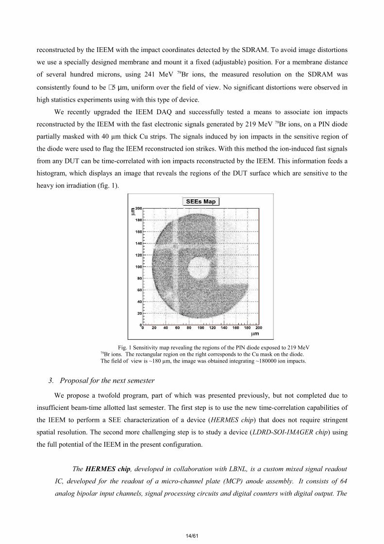
We recently upgraded the IEEM DAQ and successfully tested a means to associate ion impacts
reconstructed by the IEEM with the fast electronic signals generated by 219 MeV 79Br ions, on a PIN diode
partially masked with 40 µm thick Cu strips. The signals induced by ion impacts in the sensitive region of
the diode were used to flag the IEEM reconstructed ion strikes. With this method the ion-induced fast signals
from any DUT can be time-correlated with ion impacts reconstructed by the IEEM. This information feeds a
histogram, which displays an image that reveals the regions of the DUT surface which are sensitive to the
heavy ion irradiation (fig. 1).
Fig. 1 Sensitivity map revealing the regions of the PIN diode exposed to 219 MeV 79Br ions. The rectangular region on the right corresponds to the Cu mask on the diode. The field of view is ~180 µm, the image was obtained integrating ~180000 ion impacts.
3. Proposal for the next semester
We propose a twofold program, part of which was presented previously, but not completed due to
insufficient beam-time allotted last semester. The first step is to use the new time-correlation capabilities of
the IEEM to perform a SEE characterization of a device (HERMES chip) that does not require stringent
spatial resolution. The second more challenging step is to study a device (LDRD-SOI-IMAGER chip) using
the full potential of the IEEM in the present configuration.
The HERMES chip, developed in collaboration with LBNL, is a custom mixed signal readout
IC, developed for the readout of a micro-channel plate (MCP) anode assembly. It consists of 64
analog bipolar input channels, signal processing circuits and digital counters with digital output. The
14/61
MCP anode is being built by the Japanese Space Agency (JAXA) for the Mercury Plasma Particle
Experiment (MPPE) instrument. The MPPE is part of the payload for the Mercury Magnetospheric
Orbiter (MMO) on the Bepi Colombo mission to Mercury, a joint science mission between JAXA and
ESA.
The result of JAXA testing indicates that the HERMES chip exhibits a lower than expected SEL
(Single Event Latchup) tolerance of 12 MeV/mg/cm2 (Cl) for the analog power supply only. Nominal
current is 38 mA, current under latch-up is 114 mA.
A project to re-layout the HERMES analog circuitry for improved SEL hardening is planned in
the fall of 2010. It would be very beneficial to determine specifically the part of the circuit that is SEL
sensitive. We will build a SEL-sensitive map by using the latch-up signal to flag the corresponding
ion impacts reconstructed by the IEEM. We believe that, if we could locate the source of the problem
to within tens of microns, re-layout work would be significantly reduced and our understanding of
potential weaknesses in the layout topology would be increased.
The LDRD-SOI-IMAGER is a monolithic pixel sensor developed in the framework of the INFN
SOIPD experiment and is realised in a 0.20 µm Fully Depleted SOI technology. SOI technology
allows the fabrication of CMOS integrated circuits on a thin Silicon layer, electrically isolated from
the rest of the silicon wafer by means of a thick oxide layer. The isolation of the electronics from a
high-resistivity silicon substrate, used as the sensitive volume, allows the production of monolithic
pixel sensors for particle tracking and imaging. SOI devices were once considered more radiation
hardened than the ones manufactured in bulk technology, but SEU tests on modern SOI static random
access memories showed unexpectedly high SEU cross-sections [6]. The integrated readout
electronics of SOI monolithic pixel sensor have to be carefully studied with energetic heavy ions to
measure the effective sensitivity to SEE, in order to assess the application limits.
4. Beam time required
For the SEE test of the HERMES chip, taking into account the time needed for: 1) the IEEM
calibration at the beginning of each irradiation; 2) the beam extraction, transport and settings; 3) the time
needed to scan the most sensitive regions of the device and to collect enough statistics, we estimate that two
consecutive days of beam time are required. This experiment should be in October, to match the schedule
of the HERMES project.
Even for the SEE test of the SOI-IMAGER chip we estimate that two days of beam time are
required, possibly in November .
One of us is a PhD student (third year) who needs data of both experiments for the completion of the
thesis work, that has been founded by Fondazione Cariparo to assess the radiation tolerance of SOI sensors.
15/61

IMPORTANT NOTES:
1) We would prefer to have the possibility to access the Experimental Hall 1 some days before
each run, for installation and tests of the experimental set-up.
2) These novel experiments are performed with the by-pass (access with beam). It is extremely
important that the shifts be scheduled on work-days, because we need the radioprotection service (not
available on week-ends) to restore the by-pass in case of accidental drop.
We require the two multi-ion sources: (16O, 28Si, 58Ni, 107Ag) and (19F, 35Cl, 79Br, 127I), with the Tandem
operating between 10.5 MV and 15 MV. The beam currents will be in the range 1 nA – 20 nA.
5. References
[1] B. L. Doyle, G. Vizkelethy, D. S. Walsh, B. Senftinger and M. Mellon, “A new approach to
nuclear microscopy: the ion–electron emission microscope”, Nucl. Instr. Meth. B, 158 (1999) 6.
[2] D. Bisello, M. Dal Maschio, P. Giubilato, A. Kaminsky, M. Nigro, D. Pantano, R. Rando, M.
Tessaro and J. Wyss “A novel sensor for ion electron emission microscopy”, Nucl. Instr. Meth. B, 219
(2004) 1000.
[3] D. Bisello, P. Giubilato, S. Mattiazzo, M. Nigro, D. Pantano, R. Rando, L. Silvestrin, M. Tessaro,
J. Wyss, “Performance of the SIRAD ion electron emission microscope”, Nucl. Instr. Meth. B, 266 (2008)
2142
[4] D. Bisello, A. Candelori, P. Giubilato, A. Kaminsky, S. Mattiazzo, M. Nigro, D. Pantano, R.
Rando, L. Silvestrin, M. Tessaro, J. Wyss, “Secondary electron yield of Au and Al2O3 surfaces from swift
heavy ion impact in the 2.5–7.9 MeV/amu energy range”, Nucl. Instr. Meth. B, 266 (2008) 173.
[5] D. Bisello, P. Giubilato, S. Mattiazzo, M. Nigro, D. Pantano, R. Rando, L. Silvestrin, M. Tessaro,
J. Wyss, “Upgrade of the SIRAD IEEM”, 2008 Annual Report 128.
[6] P.E. Dodd, M.R. Shaneyfelt, K.M. Horn, D.S. Walsh, G.L. Hash, T.A. Hill, B.L. Draper, J.R.
Schwank, F.W. Sexton and P.S. Winokur, “SEU-sensitive volumes in bulk and SOI SRAMs from first-
principles calculations and experiments”, IEEE Trans. Nucl. Sci. 48 (2001) 1893.
16/61
Istituto Nazionale di Fisica Nucleare Laboratori Nazionali di Legnaro
- USP 2010 / 40- - Prot. 2518 /10 -
Beam Time Request Form 2010-06-15 18:45:55
General Information
Experiment:
Acronym : Mo.Na.De. Title:
Tuning the absorptionband in the THz range ofYBCO films patterned byHEHI lithography
Activity : Continuation Accelerator : Tandem-XTU Spokesperson: Family name : Mezzetti First name : EnricaInstitution : Dept. of Physics, Politecnico di Torino and I.N.F.N. Sez. To Address : C.so Duca degli Abruzzi 24, 10129 Torino Phone : +39-011-5647314 Fax : +39-011-5647399 E-mail : [email protected]
Participants
Family Name First Name Institution E-Mail
Enrica MezzettiDept. of Physics,Politecnico di Torino
Roberto GerbaldoDept. of Physics,Politecnico di Torino
Gianluca GhigoDept. of Physics,Politecnico di Torino
Laura GozzelinoDept. of Physics,Politecnico di Torino
Francesco LavianoDept. of Physics,Politecnico di Torino
Bruno MinettiDept. of Physics,Politecnico di Torino
Roberto CherubiniI.N.F.N. LaboratoriNazionali di Legnaro
Beams Characteristics
Ion Energy[MeV]
Intensity[pnA] Beam Channel Target ExperimentalSetup
Others...70-250MeV
lower than 1 mA Continuous +30 YBCO
Other Ion specification Pulsed Beam Requirements
Requested Beam Time
17/61
Run No. of Days Preferred PeriodAbsolutely undesiredperiod
1 2 February 20102 2 November 2010Tot. 4
Sended abstract file: xtu_Mo.Na.De._1Ab_Abstract_Proposal_Tandem_Mezzetti.pdf Sended proposal file: xtu_Mo.Na.De._2Pr_Proposal_Tandem_Mezzetti.pdf
18/61

Tuning the absorption band in the THz range of YBCO films patterned by HEHI lithography
E. Mezzetti, R. Gerbaldo, G. Ghigo, L. Gozzelino, F. Laviano, B. Minetti Dept. of Physics, Politecnico di Torino and I.N.F.N. Sezione di Torino
C.so Duca degli Abruzzi 24, 10129 Torino
R. Cherubini I.N.F.N. – Laboratori Nazionali di Legnaro
V.le Università 2, 35020 Legnaro (PD)
ABSTRACT
Far-infrared (FIR) detectors were developed in the framework of the I.N.F.N. Mo.Na.De. (Modulated Nanostructured Device) experiment. The layouts consist of suitably shaped meanders that are photolithographed on High Temperature Superconducting (HTSC) films and made functional to the FIR detection by means of the material nanostructuring induced by local High-Energy Heavy-Ion (HEHI) irradiations [1,2]. The morphology of both the superconducting film and the substrate is indeed modified by nanometric size, linearly correlated columnar defects created by HEHI beam. This HEHI-induced patterning results in a local modulation (tunable with ion fluence and energy) of the superconducting properties [3-5] of functional layouts bringing to FIR detectors that work in an almost non-dissipative state. Detector layouts grown on two selected substrates (MgO and YSZ) in quasi-static conditions exhibit remarkable performances, such as responsivity and detectivity higher than 1 V/W and 1010 cm Hz1/2 W-1, respectively, and low power dissipation [6]. Preliminary tests of radiation hardness under proton and fast neutron beams aimed at detector application in harsh environment (e.g. space environment, plasma diagnostic environment) did not reach damage threshold [7]. To fully exploit the functional behaviour of the detectors (briefly summarized in the following section) the following milestones are still needed: - downscaling of the detector active elements (spatial downscaling enhances the detector
responsivity by the increasing of ∂R/∂T) - analysis of the dynamic response in the milli- and micro-second range of the downscaled sensors - analysis of the criticality of different ion implantation depths - completing the investigation on detector radiation hardness.
19/61

Tuning the absorption band in the THz range of YBCO films patterned by HEHI lithography
E. Mezzetti, R. Gerbaldo, G. Ghigo, L. Gozzelino, F. Laviano, B. Minetti Dept. of Physics, Politecnico di Torino and I.N.F.N. Sezione di Torino
C.so Duca degli Abruzzi 24, 10129 Torino
R. Cherubini I.N.F.N. – Laboratori Nazionali di Legnaro
V.le Università 2, 35020 Legnaro (PD)
ABSTRACT
Far-infrared (FIR) detectors were developed in the framework of the I.N.F.N. Mo.Na.De (Modulated Nanostructured Device) experiment. The layouts consist of suitably shaped meanders that are photolithographed on High Temperature Superconducting (HTSC) films and made functional to the FIR detection by means of the material nanostructuring induced by local High-Energy Heavy-Ion (HEHI) irradiations [1,2]. The morphology of both the superconducting film and the substrate is indeed modified by nanometric size, linearly correlated columnar defects created by HEHI beam. This HEHI-induced patterning results in a local modulation (tunable with ion fluence and energy) of the superconducting properties [3-5] of functional layouts bringing to FIR detectors that work in an almost non-dissipative state. Detector layouts grown on two selected substrates (MgO and YSZ) in quasi-static conditions exhibit remarkable performances, such as responsivity and detectivity higher than 1 V/W and 1010 cm Hz1/2 W-1, respectively, and low power dissipation [6]. Preliminary tests of radiation hardness under proton and fast neutron beams aimed at detector application in harsh environment (e.g. space environment, plasma diagnostic environment) did not reach damage threshold [7]. To fully exploit the functional behaviour of the detectors (briefly summarized in the following section) the following milestones are still needed: - downscaling of the detector active elements (spatial downscaling enhances the detector
responsivity by the increasing of ∂R/∂T) - analysis of the dynamic response in the milli- and micro-second range of the downscaled sensors - analysis of the criticality of different ion implantation depths - completing the investigation on detector radiation hardness.
20/61

SHORT ACTIVITY REPORT AND NEXT TASKS Mo.Na.De experiment status report and next tasks Aim of the experiment Mo.Na.De. experiment is aimed at developing rugged detectors in the FIR spectrum (0.3-4 THz), required for particle beam and plasma diagnostic, security, astrophysical and medical applications. The active element of the detector is a patterned high temperature superconducting film (YBa2Cu3O7-x) nanostructured by means of High-Energy Heavy-Ion (HEHI) lithography [1-5]. Detectors work in almost dissipation-less state, minimizing the power consumption at temperature higher than the liquid nitrogen one. FIR radiation sensing element YBCO films were patterned by standard optical photolithography and wet-etching in a double meander structure (Fig. 1). One of the meanders was uniformly nanostructured by means of the Au ion beam (ion implant in the film substrate). This layout allows a simultaneous measurement of the photoresponse of as-grown (reference signal) and nanostructured (active element) YBCO [1,2].
Fig. 1
HEHI nanostructured meander V1
I+ I-
Unirradiated meander V3
V2
Next task: downscaling of the active element. This increases the element resistivity with the consequent enhancement of the responsivity. Layout solutions that contemporary guarantee high detectivity will be selected. Downscaling is also the first step towards the development of detector arrays.
FIR detection – analysis of the quasi-static response HEHI lithography locally modifies YBCO superconducting properties allowing one to obtain a functional, fluence-tunable decoupling [3,5] between the resistance (R) vs. temperature (T) characteristics of the as-grown and nanostructured meander (Fig. 2). Working temperature and bias current are then chosen in such a way that both the meanders are in a non-dissipative state, slightly below the transition temperature to zero resistance state (Tc0) of the nanostructured region (anyway above the nitrogen liquid temperature). The FIR quasi-static photoresponse is obtained by illuminating the device with a continuous-wave radiation produced by a high pressure Hg arc lamp, suitably filtered in such a way to extract the FIR components (frequencies lower than 4 THz). FIR radiation absorption brings temporarily the Au-ion nanostructured meander to a dissipative state, whereas the as-grown meander does not respond at all (Fig.3) [1,2]. Responsivity higher than 1.0 V/W and detectivity higher than 1010 Hz1/2 cm W-1 was found for YBCO film grown on CeO2-buffered YSZ substrate [6]. Next task: analysis of the dynamic response of the downscaled active element. A new FIR source for characterized the photoresponse of the detector in the milli- and micro-second range is setting up. Response time of detector grown on MgO and CeO2-buffered YSZ substrate will be compared (see below).
21/61

80 82 84 86 88 90 92 940
5
10
15
as-grown meander
nanostructured meander YBCO/CeO2/YSZ YBCO/MgO
Res
ista
nce
(kΩ
)
Temperature (K)
∆Tc0
Fig. 2 - Resistance versus temperature curves, simultaneously measured on both as-grown and nanostructured YBCO meanders grown on CeO2-buffered YSZ and MgO substrates. Au-ion nanostructuring induces a shift in the critical temperature, Tc0, defined as the temperature of the transition to a zero resistance state. (Au-ion energy: 0.114 GeV, fluence 4.84·1011 cm-2)
Fig. 3 - Real-time photoresponse of Au-nanostructured and as-grown YBCO meanders (grown on CeO2-buffered YSZ substrate) to FIR radiation produced by the arc lamp and passed through the high resistivity Si window of the cryostat and a Zitex® G110 sheet (combined transmission > 40% for wavelength in the range 75 µm – 1 mm). The bias current was 1 mA, the working temperature 79.5 K.
0 10 20 30 40 50-0.1
0.0
0.1
0.2
0.3
0.4 Au-ion irradiated YBCO as-grown YBCO
Vol
tage
(µV
)
Time (s)
filter: Si + Zitex G110
Preliminary results on substrate role in FIR photoresponse Photoresponse of YBCO films grown on CeO2-buffered YSZ, MgO and LaAlO3 substrates were analyzed. LaAlO3 was discarded because, due to its twin-boundary texturing, it does not allow obtaining a YBCO dissipation-less state for temperature higher than the liquid nitrogen one. Preliminary studies on YBCO films nanostructured with 0.114 GeV Au-ion showed that detectors grown on CeO2-buffered YSZ and MgO substrates exhibit similar responsivities in the quasi-static regime [6]. However, due to its higher thermal conductance MgO is expected to guarantee a lower response time [6]. Next task: analysis of the criticality of ion implantation depth in both the substrates. This task will be pursued by enlarging the examined Au-ion energy spectrum. The influence of substrate thermal conductivity on the dynamic response will be also addressed. Preliminary results on radiation hardness of FIR detector The reliability of our sensor under proton irradiation is based on several test performed before and after 3.5 MeV proton beam irradiation on YBCO films [5,8]. The results show a quite satisfying hardness of HEHI nanostructured YBCO films under fluences as high as 4.3·1014 cm−2 [5]. Preliminary irradiation test with fast neutrons (E > 0.1 MeV) up to a fluence of 4.5·1013 cm-2 showed that the active element do not present appreciable damage-induced shift in the transition temperature to zero resistance state for irradiation with neutron having an average energy higher than 2.0 MeV [7]. A slight increase of Tc0 was instead found after irradiation with lower energy neutron (see CN proposal for further details). Next task: Further investigation on detector radiation hardness. A systematic investigation of the sensor experimental behaviours under neutron irradiations with different energy spectra is necessary in order to achieve detector lifetime preview in harsh environment as well as to establish the radiation threshold claiming its recalibration.
22/61

Control of the vortex flow in microchannel arrays produced in YBCO films by heavy ion lithography – status report Arrays of micrometric size rows were patterned by HEHI (0.114 GeV Au-ions at a fluence of 3.4·1011 cm-2) with inclined geometries in YBCO film stripes [9]. Final goal is to investigate vortex guidance viability as well as to study the availability of power splitting lines based on the control of vortex vector velocity. Longitudinal, VL, and Hall voltage, VH, across the irradiated pattern were measured (Fig. 4). The ratio between the longitudinal and Hall voltages, VL/VH, corresponds to the ratio of the vortex velocity components, perpendicular and parallel to the current direction, respectively. In our case, this ratio is very close to the expected value of the tangent of the angle between the direction of the microchannels and the applied current in a relatively large temperature range, from about 84.5 K to 87.5 K (Fig. 5) [9]. This constitutes the striking evidence that the microchannels act as easy-flux flow channels and vortices are forced to move along their direction by the applied current flowing into the strip. These results, confirmed for different angles between the direction of the microchannels and the applied current allow us to infer that this functional arrangement of flux-flow microchannels could open the way to novel designs for the application of high temperature superconducting films as power splitter and other reciprocal three-ports elements in the microwave field. Final milestone of this experiment (power splitting of GHz signal) should be achieved using the runs scheduled in this semester January 2010- July 2010.
Fig. 4 - Voltage vs. temperature of the longitudinal and Hall voltage signals across the irradiated pattern.
Fig. 5 - Measured ratio between the longitudinal and transverse voltages. In
the temperature region comprised between 84.5 K and 87.5 K (for the
applied current of 1 mA), the ratio is very close to the theoretical value for perfect flux flow channels (1.96 = tan
(63°)).
23/61

REFERENCES
[1] F. Laviano, E. Mezzetti et al., “THz detection above 77K in YBCO films patterned by heavy-ion lithography”, IEEE Sensors 10, 863 (2010).
[2] E. Mezzetti et al., “Tuning the absorption band in the THz range of YBCO films patterned by means of HEHI lithography” Physica C, in press.
[3] F. Laviano, E. Mezzetti et al., “Local magnetic field detector made by microscale ion irradiation on high temperature superconducting films” Appl. Phys. Lett. 89, 082514 (2006).
[4] W. K. Kwok et al., “Modification of vortex behavior through heavy ion lithography”, Physica C 382, 137 (2002).
[5] R. Gerbaldo, E. Mezzetti et al., “Functional decoupling of nanostructured areas in superconducting strips for electromagnetic detectors” J. Appl. Phys. 104, 063919 (2008).
[6] E. Mezzetti “Analysis of dynamical far-infrared response of YBCO photodetectors made by Heavy Ion Lithography” presented at International Workshop on Superconductivity in Reduced Dimensions” organized by the European Science Foundation Research Networking Programme “Nanoscience and Engineering in Superconductivity”, Salzburg (Austria) 4-8 May 2010.
[7] E. Mezzetti “Rugged superconducting detector for monitoring infrared energy sources in harsh environments” presented at European Energy Conference, Barcelona (Spain) 20-23 April 2010.
[8] L. Gozzelino, D. Botta, R. Cherubini, A. Chiodoni, R. Gerbaldo, G. Ghigo, F. Laviano, B. Minetti and E. Mezzetti, “Temperature dependence of the critical current density in proton irradiated YBCO films by magneto-optical analysis” Eur. Phys. B, 40, 3 (2004).
[9] F. Laviano, E. Mezzetti et al., “Control of the vortex flow in microchannel arrays produced in YBCO films by heavy ion lithography” Physica C, in press.
BEAM TIME REQUEST
In order to fulfil the experiment milestones the following beam time is needed:
Aim Time (*)
Fabrication of new FIR detectors with downscaled layouts 44 h
Analysis of the criticality of different ion implantation depths (irradiations with different Au energies in the range 70-250 MeV)
36 h
Fabrication of detector dedicated to complete the investigation on radiation hardness (under fast neutron irradiation)
16 h
TOT 96 h To optimise the experiment, it would be preferable to have two separated runs in order to perform after-irradiation characterisations after each step and then to use feedback information. (*) the irradiation time is estimated on the basis of previous irradiations, taking into account the elapsed time for beam optimisation.
24/61
Istituto Nazionale di Fisica Nucleare Laboratori Nazionali di Legnaro
- USP 2010 / 41- - Prot. 2519 /10 -
Beam Time Request Form 2010-06-14 17:15:40
General Information
Experiment:
Acronym : SEE-NV Title:Single Event Effectson Non-volatileMemories
Activity : Continuation Accelerator : Tandem-XTU Spokesperson: Family name : Gerardin First name : SimoneInstitution : Dept. of Information Eng. - UNIPD and INFN - Padova Address : via Gradenigo 6B, 35131 Padova, Italy Phone : +390498277786 Fax : +390498277699 E-mail : [email protected]
Participants
Family Name First Name Institution E-MailAndrea Candelori INFN - PD [email protected] Cellere Applied Materials [email protected] Chimenton UNIFE [email protected] Gerardin DEI - UNIPD [email protected] Ghidini Numonyx [email protected] Greco Numonyx [email protected] Grazia Valentini Numonyx [email protected] Visconti Numonyx [email protected] Bonanomi Numonyx [email protected] Beltrami Numonyx [email protected] Bagatin DEI - UNIPD [email protected]
Beams Characteristics
Ion Energy[MeV]
Intensity[pnA] Beam Channel Target ExperimentalSetup
Others...Other Ion specification Pulsed Beam Requirements
Requested Beam Time
Run No. of Days Preferred PeriodAbsolutely undesiredperiod
1 1First week of November2010
Before October 18th 2010
2 2 December 2010 February 2011Tot. 3
25/61

Comments
We need to perform the runs from Monday to Friday and to access Exp. Hall I before the runs.
Sended abstract file: xtu_SEE-NV_1Ab_SEE-NV Abstract.pdf Sended proposal file: xtu_SEE-NV_2Pr_SEE-NV.pdf
26/61
1
Padova, June 2010
Proposal:
"Single Event Effects in Non-volatile Memories"
Marta Bagatin[1]
, Silvia Beltrami[2]
, Mauro Bonanomi[2]
, Andrea Candelori[3]
, Andrea Chimenton[4]
, Giorgio
Cellere[5]
, Simone Gerardin[1]
, Gabriella Ghidini[2]
, Eugenio Greco[2]
, Maria Grazia Valentini[2]
, Angelo Visconti[2]
* Spokesperson
[1] Dipartimento di Ingegneria dell'Informazione, Università di Padova
[2] Numonyx, Agrate Brianza, Milano
[3] INFN – Sezione di Padova
[4] Dipartimento di Ingegneria, Università di Ferrara
[5] Applied Materials Baccini, Treviso
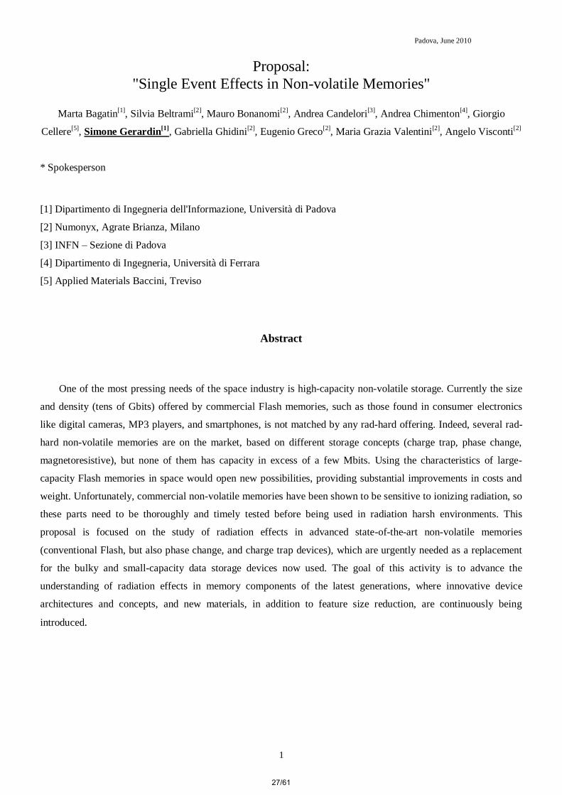
Abstract
One of the most pressing needs of the space industry is high-capacity non-volatile storage. Currently the size
and density (tens of Gbits) offered by commercial Flash memories, such as those found in consumer electronics
like digital cameras, MP3 players, and smartphones, is not matched by any rad-hard offering. Indeed, several rad-
hard non-volatile memories are on the market, based on different storage concepts (charge trap, phase change,
magnetoresistive), but none of them has capacity in excess of a few Mbits. Using the characteristics of large-
capacity Flash memories in space would open new possibilities, providing substantial improvements in costs and
weight. Unfortunately, commercial non-volatile memories have been shown to be sensitive to ionizing radiation, so
these parts need to be thoroughly and timely tested before being used in radiation harsh environments. This
proposal is focused on the study of radiation effects in advanced state-of-the-art non-volatile memories
(conventional Flash, but also phase change, and charge trap devices), which are urgently needed as a replacement
for the bulky and small-capacity data storage devices now used. The goal of this activity is to advance the
understanding of radiation effects in memory components of the latest generations, where innovative device
architectures and concepts, and new materials, in addition to feature size reduction, are continuously being
introduced.
27/61

1
Padova, June 2010
Proposal:
"Single Event Effects in Non-volatile Memories"
Marta Bagatin[1]
, Silvia Beltrami[2]
, Mauro Bonanomi[2]
, Andrea Candelori[3]
, Andrea Chimenton[4]
, Giorgio
Cellere[5]
, Simone Gerardin[1]
, Gabriella Ghidini[2]
, Eugenio Greco[2]
, Maria Grazia Valentini[2]
, Angelo Visconti[2]
* Spokesperson
[1] Dipartimento di Ingegneria dell'Informazione, Università di Padova
[2] Numonyx, Agrate Brianza, Milano
[3] INFN – Sezione di Padova
[4] Dipartimento di Ingegneria, Università di Ferrara
[5] Applied Materials Baccini, Treviso
Abstract
One of the most pressing needs of the space industry is high-capacity non-volatile storage. Currently the size
and density (tens of Gbits) offered by commercial Flash memories, such as those found in consumer electronics
like digital cameras, MP3 players, and smartphones, is not matched by any rad-hard offering. Indeed, several rad-
hard non-volatile memories are on the market, based on different storage concepts (charge trap, phase change,
magnetoresistive), but none of them has capacity in excess of a few Mbits. Using the characteristics of large-
capacity Flash memories in space would open new possibilities, providing substantial improvements in costs and
weight. Unfortunately, commercial non-volatile memories have been shown to be sensitive to ionizing radiation, so
these parts need to be thoroughly and timely tested before being used in radiation harsh environments. This
proposal is focused on the study of radiation effects in advanced state-of-the-art non-volatile memories
(conventional Flash, but also phase change, and charge trap devices), which are urgently needed as a replacement
for the bulky and small-capacity data storage devices now used. The goal of this activity is to advance the
understanding of radiation effects in memory components of the latest generations, where innovative device
architectures and concepts, and new materials, in addition to feature size reduction, are continuously being
introduced.
28/61

2
Single Event Effects in Non-volatile Memories
Single event effects are a concern not only for space applications, where trapped radiation belts, cosmic rays,
and solar activity are strong sources of ionizing particles, but also for chips at sea level, due to atmospheric
neutrons, originating from the interaction of cosmic rays with the atmosphere, and alpha particles, coming from
contaminants in the chip and solder materials.
The goal of this proposal is to make use of the SIRAD line to assess the radiation sensitivity of state-of-the art
non-volatile chips, which are very much needed by the space community, since there is currently no rad-hard non-
volatile memory part matching the size and density of commercial chips. In particular, we will study both the
transient and permanent effects of heavy ion strikes.
Recently, multi-level cell Flash memories have been shown to be sensitive to atmospheric neutrons. With this
proposal we also aim to elucidate the mechanisms leading to errors on Earth, in addition to serving the space
community, by emulating with heavy-ion beams the secondary products of the neutron interactions with chip
materials.
The experiments will be performed in the framework of a collaboration between scientists and researchers
from Italian and foreign Institutions, including an industrial partner (Numonyx), which will provide state-of-the art
devices and development test chips. The research is partially funded by MIUR. The strong scientific production of
the research performed at LNL in the area of radiation effects in non-volatile memories is shown by 14 articles
published or accepted for publication in peer-reviewed scientific journals in 2009 and 2010, in addition to 10
conference contributions presented or to be presented in 2010.
The total amount of beam time requested in the next semester at the Tandem-XTU accelerator is 3 days.
Single Event Effects in Non-volatile Memories
Beam time request: 3 days with heavy ions (ongoing experiment)
Motivations and purpose of the research
Flash Memories are attracting a lot of attention as non-volatile storage for Space applications and High Energy
Physics experiments due to their large integration and low power consumption. Yet, their radiation sensitivity has
not been fully characterized and understood, and many issues remain for their use in radiation harsh environments.
The goal of this activity is to study the behavior of Flash memories under heavy-ion irradiation, investigating
several effects which have been reported in the last few years:
charge loss from the Floating Gate (FG);
charge trapping in the dielectrics surrounding the FG;
long-term effects related to leakage paths in the tunnel oxide generated by heavy-ion irradiation;
single bit upsets originating in the peripheral circuitry (e.g., page buffer);
single event functional interruptions due to heavy-ion strikes in the embedded microcontroller;
destructive and non-destructive spikes in the supply current.
Since Floating Gate Flash memories are coming closer and closer to their scaling limits, alternative memory
concepts are being developed and will soon be ready for the consumer market. Two of the most promising
29/61

3
candidates are phase change and charge trap memories, which are expected to replace Flash NOR and NAND
devices, respectively. The radiation sensitivity of these new kinds of memories is largely unexplored. It will be
another goal of this activity to investigate single event effects (both in standy-by and during read/program/erase
operations) in these innovative devices, to assess their suitability to harsh environments. These studies are possible
thanks to our long-standing collaboration with Numonyx.
During the last year, several irradiations have been performed on a number of different technologies: 90-nm
and 65-nm NOR floating gate memories and 90-nm, 65-nm, 48-nm and 41-nm NAND samples from different
manufacturers (Numonyx, Micron, and Samsung), focusing on the sensitivity of the floating gate array. Hundreds
of Gbits were irradiated to obtain statistical significance for our results. Part of the NOR samples were previously
irradiated with x rays at the LNL. This was done to emulate the space environment, where both Total Ionizing Dose
and Single Event Effects threaten the reliability and the correct operation of electronic chips. The results have
shown an increase in the heavy-ion sensitivity of these chips as a function of the previous dose received by x rays,
which was explained based on the combination of the threshold voltage shifts induced by heavy ions and x rays.
Measurements made with reserved test modes (thanks to which we can have access to the threshold voltage of each
single cell) have been coupled with Geant4 simulations and new insight has been gained on the basic mechanisms
affecting the information stored in floating gates. In particular, a new interpretation has been found for the
transition region which originates after heavy-ion irradiation between the first and the secondary peak. The data
obtained with heavy ions have also been used to understand the scaling trends of the atmospheric neutron
sensitivity of commercial NAND samples. Unfortunately, due to the limited allocated beam time, no assessment
was carried out on the peripheral circuitry.
One day has been allocated to this activity during the last semester after the deadline for presenting this
proposal, so we cannot report on the experiments carried out during the last six months.
Proposal for the next semester
In the next semester we will continue to address the effects of single ion hits in Floating Gate devices in more
scaled samples, 32nm and less, if available. In particular, we will characterize the evolution of errors in the FG
array immediately after irradiation, as a function of the impinging ion LET. From our new measurements, we
expect to be able to better estimate the contribution to the threshold voltage shift due to charge loss and charge
trapping/detrapping/neutralization, and shed further light on the basic mechanisms. We also plan on assessing the
sensitivity of the peripheral circuitry, focusing in particular on the NAND architecture and considering functional
blocks such as the charge pumps and page buffer.
As new scaled technology will become available, we will try to understand the impact of the FG scaling on the
immediate and long-term effects, by irradiating chips belonging to different technology nodes beyond the 32-nm
one. Finally we will perform irradiations on new memory types, such as phase change and charge trap memories,
which will be supplied by Numonyx.
Recent journal publications (2010 and 2009) related to this activity
[J1] M. Bagatin, S. Gerardin, G. Cellere, A. Paccagnella, A. Visconti, S. Beltrami, M. Bonanomi, R. Harboe-Sørensen, “Annealing of
Heavy-Ion Induced Floating Gate Errors: LET and Technology Dependence,” To be published in IEEE Transactions on Nuclear Science, Aug. 2010
[J2] M. Bagatin, S. Gerardin, A. Paccagnella, G. Cellere, F. Irom, D.N. Nguyen, “Destructive Events in NAND Flash Memories Irradiated with Heavy Ions”, to be published in Microelectronics Reliability
30/61

4
[J3] S. Gerardin, M. Bagatin, A. Paccagnella, G. Cellere, A. Visconti, M. Bonanomi, “Impact of Total Dose on Heavy-ion Upsets in
Floating Gate Arrays”, to be published in Microelectronics Reliability [J4] F. Irom, D. N. Nguyen, M. Bagatin, G. Cellere, S. Gerardin, A. Paccagnella, “Catastrophic Failure in Highly Scaled Commercial
NAND Flash Memories,” IEEE Transactions on Nuclear Science, vol.57, no.1, pp.266-271, Feb. 2010 [J5] M. Bagatin, G. Cellere, S. Gerardin, A. Paccagnella, A. Visconti, S. Beltrami, “TID Sensitivity of NAND Flash Memory Building
Blocks,” IEEE Transactions on Nuclear Science, vol. 56, pp. 1909-1913, Aug. 2009 [J6] M. Bagatin, S. Gerardin, G. Cellere, A. Paccagnella, A. Visconti, M. Bonanomi, S. Beltrami, “Error Instability in Floating Ga te
Flash Memories Exposed to TID,” IEEE Transactions on Nuclear Science, vol. 56, pp. 3267-3273, Dec. 2009 [J7] G. Cellere, S. Gerardin, M. Bagatin, A. Paccagnella, A. Visconti, M. Bonanomi, S. Beltrami, R. Harboe-Sorensen, A. Virtanen, P.
Roche, “Can Atmospheric Neutrons Induce Soft Errors in NAND Floating Gate Memories?,” IEEE Electron Device Letters, vol. 30, pp. 178-180, Feb. 2009
[J8] A. Gasperin, E. Amat, J. Martin, M. Porti, M. Nafria, A. Paccagnella, “Peculiar characteristics of nanocrystal memory cells programming window,” Journal of Vacuum Science \& Technology B, vol. 27, pp. 512-516, Jan.-Feb. 2009
[J9] A. Gasperin, E. Amat, M. Porti, J. Martin-Martinez, M. Nafria, X. Aymerich, A. Paccagnella, “Effects of the Localization of the Charge in Nanocrystal Memory Cells,” IEEE Transactions on Electron Devices, vol. 56, pp. 2319-2326, Oct. 2009
[J10] A. Gasperin, A. Paccagnella, G. Ghidini, A. Sebastiani, “Heavy Ion Irradiation Effects on Capacitors With SiO2 and ONO as Dielectrics,” IEEE Transactions on Nuclear Science, vol. 56, pp. 2218-2224, Aug. 2009
[J11] A. Griffoni, S. Gerardin, P. J. Roussel, R. Degraeve, G. Meneghesso, A. Paccagnella, E. Simoen, C. Claeys, “A Statistical
Approach to Microdose Induced Degradation in FinFET Devices,” IEEE Transactions on Nuclear Science, vol. 56, pp. 3285-3292, Dec. 2009
[J12] A. Griffoni, M. Silvestri, S. Gerardin, G. Meneghesso, A. Paccagnella, B. Kaczer, M. d. P. de ten Broeck, R. Verbeeck, A. Nackaerts, “Dose Enhancement Due to Interconnects in Deep-Submicron MOSFETs Exposed to X-Rays,” IEEE Transactions on Nuclear Science, vol. 56, pp. 2205-2212, Aug. 2009
[J13] A. Paccagnella, S. Gerardin, G. Cellere, “Radiation damage on dielectrics: Single event effects,” Journal of Vacuum Science \& Technology B, vol. 27, pp. 406-410, Jan.-Feb. 2009
[J14] M. Porti, N. Nafria, S. Gerardin, X. Aymerich, A. Cester, A. Paccagnella, G. Ghidini, “Implanted and irradiated SiO2/Si structure
electrical properties at the nanoscale,” Journal of Vacuum Science \& Technology B, vol. 27, pp. 421-425, Jan.-Feb. 2009
Recent conference presentation (2010) related to this activity
[C1] M. Bagatin, S. Gerardin, A. Paccagnella, G. Cellere, A. Visconti, M. Bonanomi, “Increase in the Heavy-ion Upset Cross Section of
Floating Gate Calls Previously Exposed to TID”, to be presented at 47th IEEE Nuclear Space Radiation Effects Conference (NSREC), Denver, USA, 19-23 July 2010
[C2] M. Bagatin, S. Gerardin, A. Paccagnella, F. Faccio, “Impact of NBTI Aging on the Single Event Upset of SRAM”, to be presented at 47th IEEE Nuclear Space Radiation Effects Conference (NSREC), Denver, USA, 19-23 July 2010
[C3] M. Bagatin, S. Gerardin, A. Paccagnella, G. Cellere, F. Irom, D.N. Nguyen, “Destructive Events in NAND Flash Memories Irradiated with Heavy Ions”, to be presented at 21st European Symposium on Reliability of Electron Devices, Failure Physics and Analysis (ESREF), Monte Cassino Abbey and Gaeta, Italy, 11-15 October 2010
[C4] M. Bagatin, S. Gerardin, A. Paccagnella, “Effects of Ionizing Radiation in Flash Memories”, CMOS Emerging Technologies
(CMOSET), Whistler, BC, Canada, 19-21 May 2010 [C5] M. Bagatin, S. Gerardin, A. Paccagnella, G. Cellere, A. Visconti, “Impact of Scaling on the Heavy-ion Upset Cross Section of
Multi-Level Floating Gate Cells,” to be presented at 11th RADiation Effects on Components and Systems, Längenfeld, 20-24 September 2010
[C6] S. Gerardin, M. Bagatin, A. Paccagnella, G. Cellere, A. Visconti, S. Beltrami, C. Andreani, G. Gorini, C.D. Frost, “Scaling Trends of Neutron Effects in MLC NAND Flash Memories”, International Reliability Physics Symposium (IRPS), Anaheim, USA, 2-6 May 2010
[C7] S. Gerardin, M. Bagatin, A. Paccagnella, G. Cellere, A. Visconti, M. Bonanomi, A. Hjalmarsson, A. Prokofiev, “Heavy-ion Induced Threshold Voltage Tails in Floating Gate Arrays”, to be presented at 47th IEEE Nuclear Space Radiation Effects
Conference (NSREC), Denver, USA, 19-23 July 2010 [C8] S. Gerardin, A. Paccagnella, “Present and Future Non-volatile Memories for Space,” to be presented at 47th IEEE Nuclear Space
Radiation Effects Conference (NSREC), Denver, USA, 19-23 July 2010 [C9] S. Gerardin, M. Bagatin, A. Paccagnella, G. Cellere, A. Visconti, M. Bonanomi, “Impact of Total Dose on Heavy-ion Upsets in
Floating Gate Arrays”, to be presented at 21st European Symposium on Reliability of Electron Devices, Failure Physics and Analysis (ESREF), Monte Cassino Abbey and Gaeta, Italy, 11-15 October 2010
[C10] S. Gerardin, M. Bagatin, A. Paccagnella, G. Cellere, A. Visconti, E. Greco, “Heavy-Ion Induced Threshold Voltage Shifts in Sub 70-nm Charge-Trap Memory Cells,” to be presented at 11th RADiation Effects on Components and Systems, Längenfeld, 20-24
September 2010
31/61

5
ISTITUTO NAZIONALE DI FISICA NUCLEARE For internal use only
LABORATORI NAZIONALI DI LEGNARO Proposal n.__________
Period: _____________
A-BEAM TIME REQUEST
2.5 MV Van de Graaff AN 2000 7 MV Van de Graaff CN TANDEM/ALPI complex, please specify
TANDEM-XTU
Tandem+ALPI
Experiment title: Single Event Effects in Non-volatile Memories Spokesperson: dr. Simone Gerardin
Home Institution: Università di Padova – Dipartimento di Ingegneria dell’Informazione
Address: via Gradenigo 6B, 35131 Padova Phone: +39 049 827 7786 Fax: +39 049 827 7699 e-mail: [email protected]
BEAM CHARACTERISTICS:
In the following Table we have reported the typical beam characteristics by considering the most probable ion
with the Tandem operating at 14 MeV and two strippers. For each run, a subset from the ion species reported in the following Table will be selected according to the specific necessities of the various experiments, i.e., with the
Tandem operating between 10.5 MV and 15 MV and one or two strippers.
ION
ENERGY
[MeV]
CURRENT
[nA]
BEAM
cont. or pulse
CHANNEL
TARGET
EXPERIMENTAL
SET-UP 16O 108.68 1-10 nA Cont +70 ---- SIRAD 19F 122.68 1-10 nA Cont +70 ---- SIRAD 28Si 157.68 1-10 nA Cont +70 ---- SIRAD 35Cl 171.68 1-10 nA Cont +70 ---- SIRAD 58Ni 220.68 1-10 nA Cont +70 ---- SIRAD 79Br 241.68 1-10 nA Cont +70 ---- SIRAD
107Ag 266.68 1-10 nA Cont +70 ---- SIRAD 127I 276.68 1-10 nA Cont +70 ---- SIRAD
PULSE BEAM REQUIREMENTS: None
REQUESTED BEAM TIME AT THE TANDEM-XTU ACCELERATOR: 3 days
We would prefer to have runs of one day (24 hours) in the following periods, in order of preference:
1 days (24 hours) of irradiation from October 18th to mid-November 2010;
2 days (24+24 hours) of irradiation in December 2010;
Due to sample and personnel availability, our runs cannot be scheduled before October 18th.
COMMENTS:
We need:
to perform the runs during working days from Monday to Friday;
to have the possibility to access the Experimental Hall 1 the day before each run for installation and tests of
the experimental set-up.
32/61

Istituto Nazionale di Fisica Nucleare Laboratori Nazionali di Legnaro
- USP 2010 / 42- - Prot. 2520 /10 -
Beam Time Request Form 2010-06-15 21:07:18
General Information
Experiment:
Acronym : SEEPMOS Title:Single Event Effects onPower MOSFET
Activity : New Accelerator : Tandem-XTU Spokesperson: Family name : Busatto First name : GiovanniInstitution : DAEIMI - University of Cassino Address : Via G. Di Biasio, 43 Phone : 07762993699 Fax : 07762994325 E-mail : [email protected]
Participants
Family Name First Name Institution E-Mail
Jeff WyssINFN Padova - DIMSAT,Università di Cass
Fracesco VelardiINFN Pisa - DAEIMI,Università di Cassin
Annunziata SanseverinoINFN Pisa - DAEIMI,Università di Cassin
Francesco IannuzzoINFN Pisa - DAEIMI,Università di Cassin
Ferruccio FrisinaST-Microelectronics -Catania - Italy
Giuseppe CurròST-Microelectronics -Catania - Italy
Alessandra CascioST-Microelectronics -Catania - Italy
Dario BiselloINFN Padova - Dipartimentodi Fisica, Un
Beams Characteristics
Ion Energy[MeV]
Intensity[pnA] Beam Channel Target ExperimentalSetup
Others... 275 1-20nA Continuous +70 ------ SIRADOthers... 240 1-20nA Continuous +70 ------ SIRADOther Ion specification Pulsed Beam Requirements
Requested Beam Time
33/61
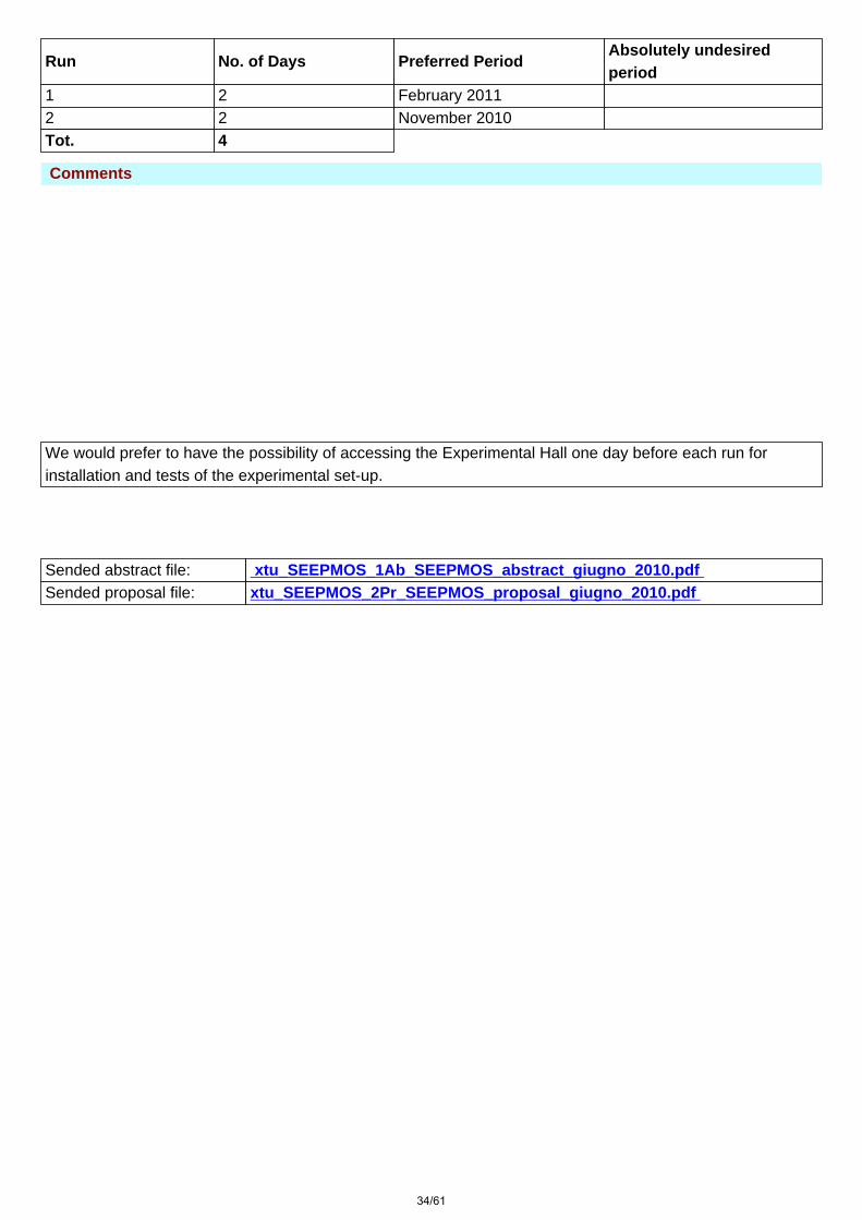
Run No. of Days Preferred PeriodAbsolutely undesiredperiod
1 2 February 20112 2 November 2010Tot. 4
Comments
We would prefer to have the possibility of accessing the Experimental Hall one day before each run forinstallation and tests of the experimental set-up.
Sended abstract file: xtu_SEEPMOS_1Ab_SEEPMOS_abstract_giugno_2010.pdf Sended proposal file: xtu_SEEPMOS_2Pr_SEEPMOS_proposal_giugno_2010.pdf
34/61

SEEPMOS Proposal:
“Single Event Effects on Power MOSFET”
D. Bisello1,2, G. Busatto3,4,*, A. Cascio5, G. Currò5, F. Frisina5,
F. Iannuzzo3,4, A. Sanseverino3, F. Velardi3,4, J. Wyss6,2
* Spokesperson
1 Dipartimento di Fisica, Università di Padova, Italy 2 INFN Padova,Italy 3 DAEIMI – Università degli Studi di Cassino - via G. Di Biasio, 43 - 03043 Cassino (FR) 4 INFN Pisa,Italy 5 ST-Microelectronics - Catania - Italy 6 DIMSAT - Università degli Studi di Cassino
Abstract
Power MOSFET are important devices to be used in power converters for the space applications.
Although a large amount of work has been dedicated so far to the study of Single Event Effects during heavy
ions irradiation on these devices, many aspects of the failure mechanisms are not clear yet. In particular the
nature and the physical mechanisms that induce the formation of latent defects in these devices requires more
investigations in order to develop new families of radiation hardened devices.
The experiment is in cooperation with the industrial partner ST-Microelectronics within the mainframe
of the Galileo European Project in cooperation with European Space Agency (ESA) and the French “Centre
National d'Etudes Spatiales” (CNES).
Power MOSFET rated at 50V and 100V will be tested with the aim of identifying the test conditions at
which latent damages are formed and the area of the chip which is sensitive to the formation of such
damages. The objective of the research activity is to study the gate damage mechanisms during the
irradiation with 79Br @ 240MeV and 197Au@275MeV with the help of a 3D finite element simulation.
A first experiment is devoted to identify the test condition for the latent damages to take place. For the
second experiment the Electron Microscope of the SIRAD irradiation facility will be used in combination
with SEE experimental set-up in order to localize the positions of each impact and to correlate them to the
damages detected in the samples under test. The objective is to identify the latente damage formation
sensitive area.
We are applying for a request of 4 days of Tandem-XTU beam to be assigned in slots of 2 days
(preferred periods: November 2010 and February 2011).
35/61

SEEPMOS Proposal:
“Single Event Effects on Power MOSFET”
D. Bisello1,2, G. Busatto3,4,*, A. Cascio5, G. Currò5, F. Frisina5,
F. Iannuzzo3,4, A. Sanseverino3, F. Velardi3,4, J. Wyss6,2
* Spokesperson
1 Dipartimento di Fisica, Università di Padova, Italy 2 INFN Padova,Italy 3 DAEIMI – Università degli Studi di Cassino - via G. Di Biasio, 43 - 03043 Cassino (FR) 4 INFN Pisa,Italy 5 ST-Microelectronics - Catania - Italy 6 DIMSAT - Università degli Studi di Cassino
Abstract
Power MOSFET are important devices to be used in power converters for the space applications.
Although a large amount of work has been dedicated so far to the study of Single Event Effects during heavy
ions irradiation on these devices, many aspects of the failure mechanisms are not clear yet. In particular the
nature and the physical mechanisms that induce the formation of latent defects in these devices requires more
investigations in order to develop new families of radiation hardened devices.
The experiment is in cooperation with the industrial partner ST-Microelectronics within the mainframe
of the Galileo European Project in cooperation with European Space Agency (ESA) and the French “Centre
National d'Etudes Spatiales” (CNES).
Power MOSFET rated at 50V and 100V will be tested with the aim of identifying the test conditions at
which latent damages are formed and the area of the chip which is sensitive to the formation of such
damages. The objective of the research activity is to study the gate damage mechanisms during the
irradiation with 79Br @ 240MeV and 197Au@275MeV with the help of a 3D finite element simulation.
A first experiment is devoted to identify the test condition for the latent damages to take place. For the
second experiment the Electron Microscope of the SIRAD irradiation facility will be used in combination
with SEE experimental set-up in order to localize the positions of each impact and to correlate them to the
damages detected in the samples under test. The objective is to identify the latente damage formation
sensitive area.
We are applying for a request of 4 days of Tandem-XTU beam to be assigned in slots of 2 days
(preferred periods: November 2010 and February 2011).
36/61
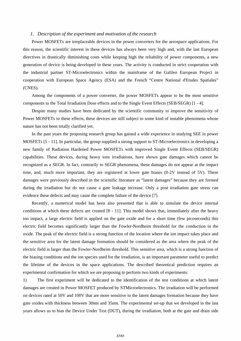
1. Description of the experiment and motivation of the research Power MOSFETs are irreplaceable devices in the power converters for the aerospace applications. For
this reason, the scientific interest in these devices has always been very high and, with the last European
directives in drastically diminishing costs while keeping high the reliability of power components, a new
generation of device is being developed in these years. The activity is conducted in strict cooperation with
the industrial partner ST-Microelectronics within the mainframe of the Galileo European Project in
cooperation with European Space Agency (ESA) and the French “Centre National d'Etudes Spatiales”
(CNES).
Among the components of a power converter, the power MOSFETs appear to be the most sensitive
components to the Total Irradiation Dose effects and to the Single Event Effects (SEB/SEGR) [1 - 4].
Despite many studies have been dedicated by the scientific community to improve the sensitivity of
Power MOSFETs to these effects, these devices are still subject to some kind of instable phenomena whose
nature has not been totally clarified yet.
In the past years the proposing research group has gained a wide experience in studying SEE in power
MOSFETs [5 - 11]. In particular, the group supplied a strong support to ST-Microelectronics in developing a
new family of Radiation Hardened Power MOSFETs with improved Single Event Effects (SEB/SEGR)
capabilities. These devices, during heavy ions irradiations, have shown gate damages which cannot be
recognized as a SEGR. In fact, contrarily to SEGR phenomena, these damages do not appear at the impact
time, and, much more important, they are registered at lower gate biases (0-2V instead of 5V). These
damages were previously described in the scientific literature as “latent damages” because they are formed
during the irradiation but do not cause a gate leakage increase. Only a post irradiation gate stress can
evidence these defects and may cause the complete failure of the device [7].
Recently, a numerical model has been also presented that is able to simulate the device internal
conditions at which these defects are created [8 - 11]. This model shows that, immediately after the heavy
ion impact, a large electric field is applied on the gate oxide and for a short time (few picoseconds) this
electric field becomes significantly larger than the Fowler-Nordheim threshold for the conduction in the
oxide. The peak of the electric field is a strong function of the location where the ion impact takes place and
the sensitive area for the latent damage formation should be considered as the area where the peak of the
electric field is larger than the Fowler-Nordheim threshold. This sensitive area, which is a strong function of
the biasing conditions and the ion species used for the irradiation, is an important parameter useful to predict
the lifetime of the devices in the space applications. The described theoretical prediction requires an
experimental confirmation for which we are proposing to perform two kinds of experiments:
1) The first experiment will be dedicated to the identification of the test conditions at which latent
damages are created in Power MOSFET produced by STMicroelectronics. The irradiation will be performed
on devices rated at 50V and 100V that are more sensitive to the latent damages formation because they have
gate oxides with thickness between 30nm and 35nm. The experimental set-up that we developed in the last
years allows us to bias the Device Under Test (DUT), during the irradiation, both at the gate and drain side
37/61

with a variable voltage and to measure the leakage current at the gate with a resolution of 10pA. Moreover,
the current pulses, that are collected at the external leads due to the charge generated during the ions impacts,
are acquired by a fast sampling wide band digital oscilloscope. A post irradiation analysis allows us to
perform a statistical analysis and to correlate the amount of the charge generated to the entity of the gate
damage.
2) In the second experiment we want to use the Electron Microscope of the SIRAD irradiation facility
in combination with our experimental set-up in order to localize the positions of each impact and to correlate
them to the current pulses acquired by the oscilloscope. The real positions of each impact in combination
with the measure of the increase of the leakage gate current during the irradiation will allow us to identify the
sensitivity area of the device to the formation of latent damages.
Two species, namely 79Br at 241.68MeV and 197Au at 275.68MeV, will be used for the irradiation
experiments. SRIM simulations show, for these two species, energy losses at the surface equal to 900eV/Å
and 1500 eV/Å and ranges 25μm and 18μm, respectively. In particular Br ions have a larger range and a
lower charge generated at the surface than the Au, so that we will be able to study separately the effects of
the charge deposited at the surface and those ones due to the ranges of the particles.
2. Proposal for the next semester
The experiment is the continuation of a long series of experiments performed between 2004 and 2008
on power MOSFET fabricated by ST-Microelectronics devoted to understand the physical reasons of Single
Event Effects (SEB/SEGR) in Power MOSFETs. We plan to perform SEGR experiments at low gate
voltages on the latest generation of 50V and 100V power MOSFET produced by ST-Microelectronics. The
formation of latent damages have been evidenced by previous experiments on these devices at these
conditions. We are proposing to use the SIRAD irradiation facility no 70° line and in particular to use the
Electron Microscope that is installed in that line.
Aim of the proposed experiments is to identify the test conditions at which latent damages are created
during the irradiation with 79Br and 197Au. Moreover the area of the chip sensitive to the formation of latent
damages and the related cross section will be identified. We are proposing to use a flux of ~500ions/cm2 of 79Br at 241.68MeV and 197Au at 275.68MeV for the reasons explained in the previous section.
3. Beam time required
We plan to obtain the required values of LET and ranges by changing the ion species, the typology of
the devices to be tested and the test conditions. Taking into account the time needed for data acquisition and
the time to set the two beams, we estimate that for the two experiments 4 days should be necessary to be
assigned in slots of 2 days (preferred periods: November 2010 and February 2011).
We would prefer to have the possibility to access the Experimental Hall 1 the day before each run for
installation and tests of the experimental set-up. We require the two multi-ion sources necessary for Br and
38/61

Au, with the Tandem operating between 13 MV and 15 MV. The beam currents will be in the range 1nA -
20nA.
4. Bibliografia
1. J.H. Hohl, G.H.Johnson, "Features of the Triggering Mechanism for Single Event Burnout of Power MOSFETs," IEEE Trans. Nuc. Sci., Vol.36, No.6, December 1989, pp.2260-2266;
2. E.G. Stassinopoulos, et al. "Charge Generation by Heavy Ions in Power MOSFETs, Burnout Space Predictions, and Dynamic SEB Sensitivity," IEEE Trans. Nuc. Sci., Vol.36, No.6, December 1992, pp.1704-1711;
3. J.L. Titus, C.F. Wheatley, "Experimental Studies of Single-Event Gate Rupture and Burnout In Vetical Power MOSFET's," IEEE Trans. Nuc. Sci., Vol.46, No.2, April 1996, pp.533-545;
4. M. Allenspach, et al. " SEGR and SEB in N-Channel Power MOSFETs," IEEE Trans. Nuc. Sci., Vol.43, No.6, December 1996, pp.2927-2931;
5. F. Velardi, F. Iannuzzo, G. Busatto, A. Porzio, A. Sanseverino, G. Currò, A. Cascio, F. Frisina, “The Role of the Parasitic BJT Parameters on the Reliability of New Generation Power MOSFET during Heavy Ion Exposure” Microelectronics Reliability, Vol. 44, No. 9-11, pp. 1407-1411, settembre - novembre 2004.
6. G. Busatto, A. Porzio, F. Velardi, F. Iannuzzo, A. Sanseverino, G. Currò: “Experimental and Numerical investigation about SEB/SEGR of Power MOSFET” Microelectronics Reliability, Vol.45, No. 10-14, pp. 1711-1716, October 2005.
7. G. Busatto, F. Iannuzzo, A. Porzio, A. Sanseverino, F. Velardi and G. Currò, "Experimental study of power MOSFET’s gate damage in radiation environment", Microelectronics and Reliability, Vol. 46, No. 9-11, pp. 1854-1857, September - November 2006.
8. A. Porzio, F. Velardi, G. Busatto, F. Iannuzzo, A. Sanseverino, G. Currò: “A 3-D Simulation Study about Single Event Gate Damage in Medium Voltage Power MOSFET” Proc. 8th Radiation and its effects on components and Systems, RADECS 2008 - Settembre 2008, Yvanskjla, Finlandia
9. G. Busatto, G. Currò, F. Iannuzzo, A. Porzio, A. Sanseverino, F. Velardi: “Experimental Evidence of “Latent Gate Oxide Damages” in Medium Voltage Power MOSFET as a Result of Heavy Ions Exposure” Microelectronics and Reliability, Vol. 48, No. 8-9, pp. 1306-1309, September - November 2008.
10. G. Busatto, G. Currò, F. Iannuzzo, A. Porzio, A. Sanseverino and F. Velardi, “Experimental Study about Gate Oxide Damages in Patterned MOS Capacitor Irradiated with Heavy Ions”, Microelectronics and Reliability, Vol. 49, Issues 9-11, pp. 1033-1037, September-November 2009.
11. G. Busatto, G. Currò, F. Iannuzzo, A. Porzio, A. Sanseverino, F. Velardi, “Heavy-Ion Induced Single Event Gate Damage in Medium Voltage Power MOSFETs”, IEEE Transactions on Nuclear Science, Vol. 56, No. 6, Part 2,pp. 3573 - 3581, December 2009.
39/61
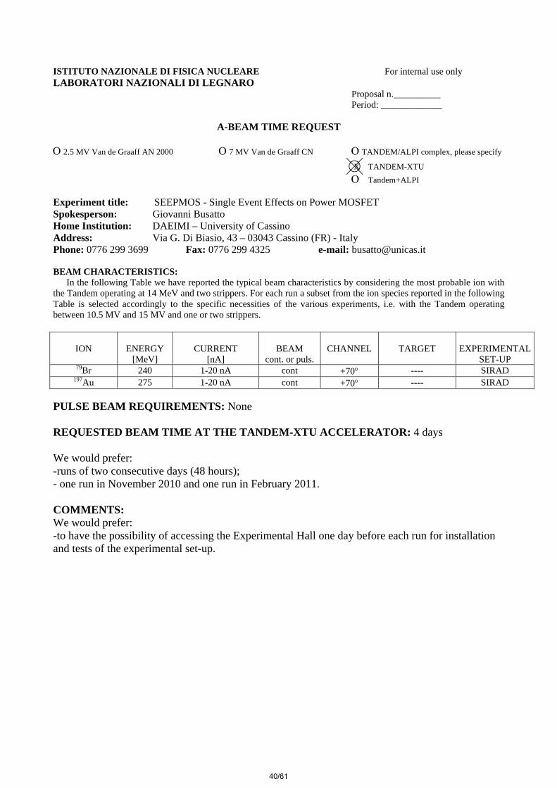
ISTITUTO NAZIONALE DI FISICA NUCLEARE For internal use only LABORATORI NAZIONALI DI LEGNARO Proposal n.__________ Period: _____________
A-BEAM TIME REQUEST
Ο 2.5 MV Van de Graaff AN 2000 Ο 7 MV Van de Graaff CN Ο TANDEM/ALPI complex, please specify
X TANDEM-XTU Ο Tandem+ALPI
Experiment title: SEEPMOS - Single Event Effects on Power MOSFET Spokesperson: Giovanni Busatto Home Institution: DAEIMI – University of Cassino Address: Via G. Di Biasio, 43 – 03043 Cassino (FR) - Italy Phone: 0776 299 3699 Fax: 0776 299 4325 e-mail: [email protected] BEAM CHARACTERISTICS:
In the following Table we have reported the typical beam characteristics by considering the most probable ion with the Tandem operating at 14 MeV and two strippers. For each run a subset from the ion species reported in the following Table is selected accordingly to the specific necessities of the various experiments, i.e. with the Tandem operating between 10.5 MV and 15 MV and one or two strippers.
ION
ENERGY
[MeV]
CURRENT
[nA]
BEAM
cont. or puls.
CHANNEL
TARGET
EXPERIMENTAL
SET-UP 79Br 240 1-20 nA cont +70° ---- SIRAD
197Au 275 1-20 nA cont +70° ---- SIRAD PULSE BEAM REQUIREMENTS: None REQUESTED BEAM TIME AT THE TANDEM-XTU ACCELERATOR: 4 days We would prefer: -runs of two consecutive days (48 hours); - one run in November 2010 and one run in February 2011. COMMENTS: We would prefer: -to have the possibility of accessing the Experimental Hall one day before each run for installation and tests of the experimental set-up.
40/61

Istituto Nazionale di Fisica Nucleare Laboratori Nazionali di Legnaro
- USP 2010 / 43- - Prot. 2521 /10 -
Beam Time Request Form 2010-06-14 17:00:59
General Information
Experiment:
Acronym : SOISEE Title:Single Event Effects onSOI pixel sensorsreadout electronics
Activity : Continuation Accelerator : Tandem-XTU Spokesperson: Family name : Bisello First name : DarioInstitution : University and INFN Padova Address : Dipartimento di Fisica Galileo Galilei, Via Marzolo 8, Padova Phone : 049-8277216 Fax : 049-8277237 E-mail : [email protected]
Participants
Family Name First Name Institution E-Mail
Wyss JefferyINFN Padova andDIMSAT
Tessaro MarioUniversity and INFNPadova
Pozzobon NicolaUniversity and INFNPadova
Silvestrin LucaUniversity and INFNPadova
Mattiazzo SerenaUniversity and INFNPadova
Contarato Devis LBNL [email protected]
Giubiliato PieroUniversity and INFNPadova
Candelori Andrea INFN Padova [email protected]
Bisello DarioUniversity and INFNPadova
Battaglia MarcoLBNL and UC SantaCruz
Beams Characteristics
Ion Energy[MeV]
Intensity[pnA] Beam Channel Target ExperimentalSetup
Others... +70 SIRADOther Ion specification Pulsed Beam Requirements NO
Requested Beam Time
41/61
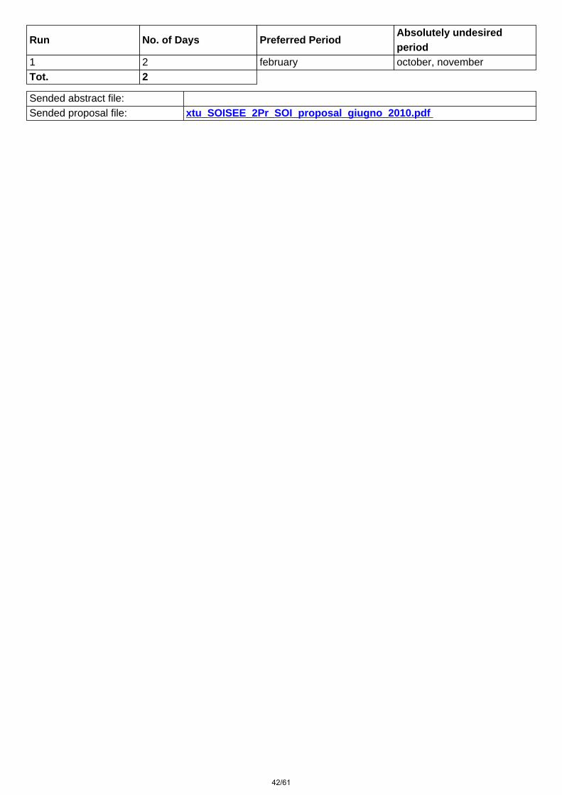
Run No. of Days Preferred PeriodAbsolutely undesiredperiod
1 2 february october, novemberTot. 2
Sended abstract file:
Sended proposal file: xtu_SOISEE_2Pr_SOI_proposal_giugno_2010.pdf
42/61

SOISEE Proposal:
“Single Event Upsets on SOI pixel sensors readout electronics”
M. Battaglia1,2, D. Bisello3,4,*, A. Candelori3,4, D. Contarato2, P. Giubilato2,3,4, S. Mattiazzo3,4, N. Pozzobon3,4,
L. Silvestrin3,4, M. Tessaro4, J. Wyss4,5
* Spokesperson
1 Department of Physics, University of California, Berkeley, CA 94720, USA.2 Lawrence Berkeley National Laboratory, Berkeley, CA 94720, USA.3 Dipartimento di Fisica, Università di Padova, Italy.4 INFN Padova, Italy.5 DiMSAT, Università di Cassino, Cassino, Italy.
Abstract
SOI technology allows the fabrication of CMOS integrated circuits on a thin Silicon layer, electrically
isolated from the rest of the silicon wafer by means of a thick oxide layer. The isolation of the electronics
from a high-resistivity silicon substrate, used as the sensitive volume, allows the production of monolithic
pixel sensors for particle tracking and imaging. Traditionally, SOI devices were considered more radiation
hardened than the ones manufactured in bulk technology and therefore considered possible candidate sensors
for tracking in the LHC upgrade (Super-LHC).
In the framework of the INFN SOIPD experiment, the LDRD-SOI-IMAGER chip has been realised in a
0.20 µm Fully Depleted SOI technology. Aim of this work is to study the SEU sensitivity of the integrated
readout electronics of this detector for high energy physics applications.
43/61

1. Description of the experiment and motivation of the researchSOI technology allows the fabrication of CMOS integrated circuits on a thin Silicon layer, electrically
isolated from the rest of the silicon wafer by means of a thick oxide layer. The isolation of the electronics
from a high-resistivity silicon substrate, used as a sensitive volume, allows the production of monolithic
pixel sensors for particle tracking and imaging. Vias etched through the oxide allows to contact the substrate
from the electronics layer, so that pixel implants can be created and reverse biased.
In the framework of the INFN SOIPD experiment, a prototype chip, named LDRD-SOI-1, has been
obtained in 2007 in a 0.15 µm Fully Depleted (FD) SOI technology, with both analog and digital pixels, and
has been extensively characterized [1],[2]. A second prototype chip (LDRD-SOI-2) has been developed and
is currently under test. It has been built in a 0.20 µm FD-SOI process, optimised for low leakage current. The
sensor has a 350 μm thick high-resistivity (700 Ω·cm) substrate. The CMOS circuitry is implanted on a
40 nm Si layer on top of a 200 nm thick buried oxide (BOX); the thickness of the CMOS layer is small
enough to be fully depleted. The chip is a 5×5 mm2 prototype with an active area of 3.5×3.5 mm2, in which
168×172 pixels are arrayed with a 20 μm pitch. The pixel matrix is subdivided into a 40×172 pixel section
with a simple analog 3-transistor architecture, mostly intended for technology evaluation, and a 128×172
pixel main section with a second-generation digital pixel cell. A third chip (LDRD-SOI-IMAGER), realised
in the same technology as the previous one, has been recently delivered. It consists of an array of 256×256
pixels (only analog, with 13.75 µm pitch), with 4 analog outputs. The two shift registers used for row and
column addressing are available on two output pads.
These detectors are being developed to work in environment with a high level of radiation.
Traditionally, SOI devices were considered more radiation hardened than the ones manufactured by bulk
technology, with respect to Single Event Effects (SEE): the charge collection volume was assumed to be
much smaller in the SOI because it was believed that charge is induced only by the carriers created in the top
silicon layer and not by the carriers created below the BOX. In the past SEU tests seemed to support this
assumption. On the contrary, most recently, new SEU tests on modern SOI static random access memories
(SRAMs with BOX thicknesses less than 200 nm) showed unexpectedly high SEU cross-sections [3]. The
measured SEU cross-section was much closer to the combined gate-drain area than to the expected gate-only
area. SEU imaging performed using a nuclear microprobe proved that the combined drain-gate area is
sensitive to SEUs. Ion Beam Induced Charge (IBIC) measurements showed that the amount of induced
charge is much larger than the charge deposited into the top silicon layer above the BOX [4],[5]. This was a
clear indication that the charge induction occurs not only when the carriers move in the top silicon layer but
also when they move below the BOX.
It is clear from the considerations above that the behaviour of the described SOI Monolithic Pixel
Sensors has to be carefully studied with energetic heavy ions to measure their effective sensitivity to Single
Event Effects, in order to assess their application limits in modern high energy physics experiments.
These measurement are of strong interest for the preparation of the Technical Design Report for the
Phase I of CMS Tracker Upgrade, which has to be presented by middle 2010.
44/61
2. Status of the experiment and previous results
In the framework of the INFN SOIPD experiment, we have performed preliminary experiments at the
SIRAD heavy ion irradiation facility to study the global SEU sensitivity of the latest SOI integrated pixel
detector (LDRD-SOI-IMAGER). The goal is to measure the SEU cross section as a function of the Linear
Energy Transfer (LET) of the impinging ions (the Weibull curve), using heavy ions with values of LET in
silicon ranging from the expected “threshold” value (∼1 MeV·cm2/mg), through the “knee” (few
MeV·cm2/mg) up into to the “plateau” region (tens of MeV·cm2/mg). The irradiation was performed with a
broad beam: i.e. the ion beam is defocused so that the flux (∼104 ions/cm2-s) is uniform on the device under
test. This global irradiation technique is the standard one at SIRAD [6]; the new Ion Electron Emission
Microscope gives complementary information (it reconstructs individual ion impact points) [7].
The global SEU study is performed by exploiting the two shift registers used by the LDRD-SOI-
IMAGER to select and scan progressively the cells lines and columns during the reading and reset operation.
In this particular design, the input and output of one of these registers are made available. This allows us to
load a known pattern of logical 0 and 1 values in one of the registers and transport it to the output. The
occurrence of one (or more) SEU in the irradiated registers is detected as an alteration of the loaded logical
sequence.
Studies in literature refer only to electronic devices where the substrate had mechanical purposes, while
we are fabricating detectors with a sensitive substrate depleted by a bias. In January 2010 we started the SEU
cross section measurements of a biased chip, exploring in particular the “knee” region of the Weibull curve;
these preliminary results suggest that the SEU sensitivity of such a device is significantly enhanced by the
bias applied to the substrate
3. Proposal for the next semester
In the next semester we aim at performing a complete SEU cross section curve, constrained by many
data points, carefully exploring the “threshold” and “knee” regions, as well as establishing the “plateaux”.
This will be done both by changing ion species and angle of incidence (by tilting the chip). For each LET
value, we will compare the effect of different substrate bias conditions: two chips, one with bias, and one
without, will be studied in sequence. This is a completely innovative work program, as no studies have been
previously performed in such conditions on this kind of devices.
The ion species available at the Tandem accelerator with a working voltage between 13 MV and 15 MV
have the necessary LET and range in silicon.
4. Beam time required
We plan to obtain the required LET values not only by changing the ion species but also by changing
the tilting angle of the sample. Taking into account the time needed for data acquisition and the time to set
the various beams, we estimate that for this experiment 2 days are necessary (preferred period: February).
45/61

We would prefer to have the possibility to access the Experimental Hall 1 at least one day before each
run for installation and tests of the experimental set-up. We require the two multi-ion sources: (16O, 28Si, 58Ni, 107Ag) and (19F, 35Cl, 79Br, 127I), with the Tandem operating between 13 MV and 15 MV. The beam currents
will be in the range 1nA - 20nA.
5. Bibliografia
[1] M. Battaglia, D. Bisello, D. Contarato, P. Denes, P. Giubilato, L. Glesener, C. Vu, “A monolithic
pixel sensor in 0.15 µm fully depleted SOI technology”, Nucl. Instr. Meth. A, 583 (2007) 526.
[2] M. Battaglia, D. Bisello, D. Contarato, P. Denes, P. Giubilato, S. Mattiazzo, L. Glesener, C. Vu,
“Monolithic pixel sensors in deep-submicron SOI technology with analog and digital pixels”, Nucl. Instr.
Meth. A, 604 (2009) 380.
[3] P.E. Dodd, M.R. Shaneyfelt, K.M. Horn, D.S. Walsh, G.L. Hash, T.A. Hill, B.L. Draper, J.R.
Schwank, F.W. Sexton and P.S. Winokur, “SEU-sensitive volumes in bulk and SOI SRAMs from first-
principles calculations and experiments”, IEEE Trans. Nucl. Sci. 48 (2001) 1893.
[4] G. Vizkelethy, P.E. Dodd, J.R. Schwank, M.R. Shaneyfelt, D.S. Walsh, F.D. McDaniel and B.L.
Doyle, “Anomalous charge collection from silicon-on-insulator structures”, Nucl. Instr. Meth. B, 210 (2003)
211.
[5] J.R. Schwank, P.E. Dodd, M.R. Shaneyfelt, G. Vizkelethy, B.L. Draper, T.A. Hill, D.S. Walsh, G.L.
Hash, B.L. Doyle and F.D. McDaniel, “Charge collection in SOI capacitors and circuits and its effect on
SEU hardness”, IEEE Trans. Nucl. Sci. 49 (2002) 2937.
[6] J. Wyss, D. Bisello and D. Pantano "SIRAD: an irradiation facility at the LNL Tandem accelerator
for radiation damage studies on semiconductor detectors and electronic devices and systems", J. Wyss, D.
Bisello and D. Pantano, Nucl. Instr. Meth. A, 462, (2001) 426.
[7] D. Bisello, A. Candelori, P. Giubilato, A. Kaminsky, S. Mattiazzo, M. Nigro, D. Pantano, R. Rando,
M. Tessaro, J. Wyss, S. Bertazzoni and D. Di Giovenale, “Ion Electron Emission Microscopy at SIRAD”,
Nucl. Instr. Meth. B, 231 (2005) 65.
46/61

Istituto Nazionale di Fisica Nucleare Laboratori Nazionali di Legnaro
- USP 2010 / 44- - Prot. 2522 /10 -
Beam Time Request Form 2010-06-15 12:54:24
General Information
Experiment:
Acronym : STARTRACK2 Title:Nanodosimetricstructure of an ion track
Activity : Continuation Accelerator : Tandem-XTU Spokesperson: Family name : Colautti First name : PaoloInstitution : LNL-INFN Address : viale dell'Università 2 Phone : 049 8068304 Fax : 049 641925 E-mail : [email protected]
Participants
Family Name First Name Institution E-MailSbrogiò Guido LNL-INFN [email protected] Marion PTB Germany [email protected] Bernd PTB Germany [email protected] Stefania LNL-INFN [email protected] Mariano LNL-INFN [email protected] Marco LNL-INFN [email protected] Gianpietro LNL-INFN [email protected] Valeria LNL-INFN [email protected] Paolo LNL-INFN [email protected] Nardo Laura Pd-INFN [email protected] Giorgio Pd-INFN [email protected] Davide Pd-INFN [email protected]
Beams Characteristics
Ion Energy[MeV]
Intensity[pnA] Beam Channel Target ExperimentalSetup
Others... 26.7 1 Continuous +50 Propane STARTRACKOthers... 26.7 1 Continuous +50 Propane STARTRACKOthers... 240 1 Continuous +50 Propane STARTRACKOther Ion specification Pulsed Beam Requirements
Requested Beam Time
Run No. of Days Preferred PeriodAbsolutely undesiredperiod
1 3 January-March 2011 October 23 - November 12 2 October 23- November 1
47/61
3 3 October 23- November 1Tot. 8
Comments
The first 2 shifts with Lithium ion are recoveries of shifts lost during the las calendar. The third shift is withCarbon-12 ions 240 MeV (Alpi accelerator).
Sended abstract file: xtu_STARTRACK2_1Ab_abstract2.pdf Sended proposal file: xtu_STARTRACK2_2Pr_STARTRACK2.pdf
48/61

STARTRACK2
P.Colautti1, V.Conte
1, D. Moro
2, M. Lombardi
1, M.Poggi
1, S.Canella
1, G.Egeni
1,
L.De Nardo2, G.Tornielli
2
1 LNL-INFN 2 PD-INFN and Physics Dep. of Padova University
ABSTRACT
Many radiobiological data point out that the biological effectiveness (radiation quality) is a local effect occurring at nanometre level. Microdosimetry describes the radiation quality in terms of ionisation-event statistical properties in a “biological significant” site. In turn, such statistical properties depend on primary particle kind, velocity, site size and its distance from the primary particle track. Monte Carlo calculations have pointed out that some statistical properties are invariant with the distance from the track. Other properties could be invariant also with particle kind and velocity. The INFN 5th scientific commission has approved a three-year experiment (2009-2011) called STARTRACK2 to verify the ionization distribution invariance with the impact parameter for some light ions of therapeutic interest, namely protons, lithium ions and carbon ions. Ionization distributions due to different ions of the same velocity, or alternatively of the same mean ionization free path, will be compared. In this experiment, the biological significant site is defined is a cylindrical volume, the mean chord of which is 2 µg/cm2, namely 20 nm at density of 1g/cm3.
The experimental set up has been mounted on the +50° beam line of the Tandem-Alpi LNL particle accelerator complex and successfully tested with a 20 MeV proton beam.
STARTRACK2 experimental schedule foresees to conclude Lithium ion measurements this year and Carbon ion measurements next year. Of the two shifts allocated in the first semester of this year, one was cancelled because of accelerator problems and the other one couldn’t be properly used because beam instabilities. Therefore, we ask two shifts of measurements with 7Li beam before the end of the year and a shift with 12C at the beginning of next year.
49/61
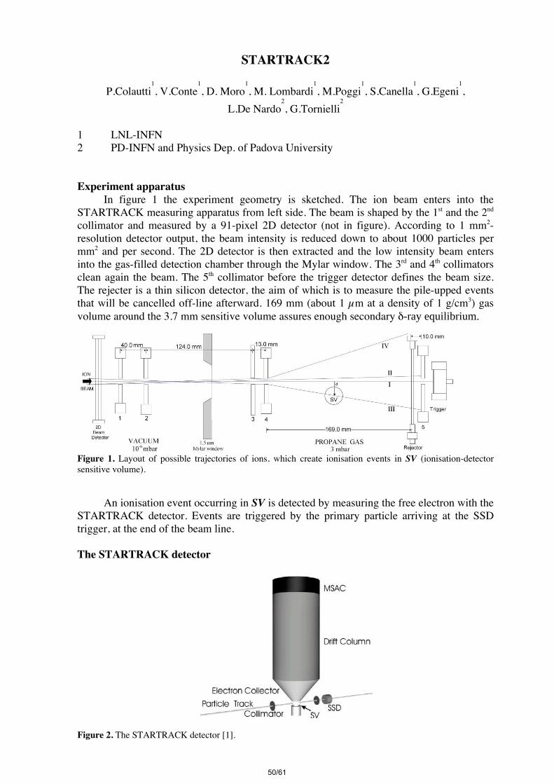
STARTRACK2
P.Colautti1, V.Conte
1, D. Moro
1, M. Lombardi
1, M.Poggi
1, S.Canella
1, G.Egeni
1,
L.De Nardo2, G.Tornielli
2
1 LNL-INFN 2 PD-INFN and Physics Dep. of Padova University Experiment apparatus
In figure 1 the experiment geometry is sketched. The ion beam enters into the STARTRACK measuring apparatus from left side. The beam is shaped by the 1st and the 2nd collimator and measured by a 91-pixel 2D detector (not in figure). According to 1 mm2-resolution detector output, the beam intensity is reduced down to about 1000 particles per mm2 and per second. The 2D detector is then extracted and the low intensity beam enters into the gas-filled detection chamber through the Mylar window. The 3rd and 4th collimators clean again the beam. The 5th collimator before the trigger detector defines the beam size. The rejecter is a thin silicon detector, the aim of which is to measure the pile-upped events that will be cancelled off-line afterward. 169 mm (about 1 µm at a density of 1 g/cm3) gas volume around the 3.7 mm sensitive volume assures enough secondary δ-ray equilibrium.
Figure 1. Layout of possible trajectories of ions, which create ionisation events in SV (ionisation-detector sensitive volume).
An ionisation event occurring in SV is detected by measuring the free electron with the STARTRACK detector. Events are triggered by the primary particle arriving at the SSD trigger, at the end of the beam line.
The STARTRACK detector
Figure 2. The STARTRACK detector [1].
50/61

The detector sensitive volume SV is defined by a static electric field, carefully constructed with several mini electrodes. SV collects the electrons and transfers them in a long electron drift column. The electrons diffuse along the column and finally arrive at the multi-step avalanche chamber (MSAC). The MSAC multiplies each electron by a factor 2*107. The MSAC signal has a rising time of less than 10 ns. That allows detecting one by one the electrons separated by about 20 ns. The average electron detection efficiency is of about 20%. The SV is a wall-less cylinder 3.7 mm of diameter and height. At 3 mbar of propane gas the SV size is about 2 µg/cm2, which corresponds to 20 nm when scaled at a density of 1 g/cm3. The detector, which is sketched in Figure 3, is mounted on a movable platform. Therefore, it can measures the ionisation events, which occur inside the 20 nm SV, at different distances, from the particle track, namely at different impact parameters. First experimental measurements with 20 MeV proton beams have been published recently [2]. Experimental aims
The experimental aim is to find some significant statistical invariance in the distributions of ionization events occurring in a 20 nm site as it is positioned at different impact parameter. Moreover, to see if such invariance holds for different ions with the same velocity or ionization mean free path λ. We have been investigating light ions of medical interest. In figure 1, the mean ionization free path is plotted against the specific energy for different ions. The two dashed lines point out ions with the same velocity (therefore, with the same ∂-ray energy spectrum) and ions with the same λ (therefore, with the same number of ∂-rays for unit of track).
Figure 3. Calculated ionisation mean free path against specific energy for 4 different ions. Green circles point out the beam that will be used in STARTRACK2 experiment.
51/61

4He measuremets. Previous measurements performed with 244Cm alpha particle had pointed out that
conditional cluster distributions are independent on the impact parameter, namely on the distance from the track [3]. That finding suggests that the biological effectiveness, or quality, of the ∂-ray cloud of 5.4 MeV 4He ions is the same everywhere. 20 MeV proton measurements
Last year, measurements and calculations have been performed with a 20 MeV proton beam. The sensitive volume has been moved from 0 nm up to 30 nm from the proton track, with steps of about 2.5 nm. At each position, electron clusters due to about 4·106 protons were collected. Conditional cluster-size distributions at different distances d in the penumbra region of a 20 MeV proton beam are shown in Figure 5. Symbols represent the measurement data, lines the results of Monte Carlo calculations. Both calculated and measured data point out the invariance of the conditional distribution with respect to the impact parameter d.
Figure 5. Conditional ionisation cluster-size distributions in 20 nm sites at different distances d from a 20 MeV proton beam (left side).
Figure 6. Conditional ionization cluster-size distributions at impact parameter d=30 nm. Filled circles: 20 MeV protons; open circles: 5.4 MeV alpha particles. Full line: protons MC calculation; dashed-line: alpha-particles MC calculation.
In Figure 6, conditional cluster-size distributions in a site placed at 30 nm from a 20
MeV proton-track and from a 5.5 MeV 244Cm alpha-particle track are plotted together. Both measured and calculated data do not show any difference between the two conditional distributions (experimental results have been presented at the XV Microdosimetric Symposium [4]). Further measurements were performed with 16 MeV deuteron beam, which has the same ∂-ray cloud as the 8 MeV proton beam. Lithium ion measurements: beam time needs
STARTRACK2 is a three year experiment approved by the INFN 5th scientific commission. The milestone for 2010 is completing the measurements with 7Li ions. Unfortunately two runs have been missed in 2010. The first one in January 2010, because a bad control in beam delivering caused a burnt out of the front-end electronics. The second shift in may 2010 was cancelled because of a shut down of the Tandem accelerator. Data analysis of measurements with 8 MeV/amu Lithium ions are in progress.
In order to conclude the Lithium measurements within the 2010 year, we need two shifts at 3.82 MeV/amu of specific energy. At such energy the Lithium ion is expected to have an ionization mean free path of 0.57 nm as a Carbon ion of 20 MeV/amu (see figure 3). Therefore, we ask 2 shifts with 7Li (26.7 MeV) in 2010. The 3 days shift is necessary for measurements at impact parameter d lower than 30 nm) and one of 2 days (for
52/61
measurements at impact parameter d bigger than 30 nm. It is in fact necessary to remember that a single measurements point in the ∂-ray cloud needs about 107 counts with the actual maximum acquisition rate of 500 Hz. That means about 6 hours of measurement time.
Carbon ion measurements: beam time needs
STARTRACK2 milestone for 2011 is completing measurements with Carbon ions. We ask therefore to have a 3 day shift of 20 MeV/amu Carbon ion (240 MeV of energy) in the period January-march 2011. References 1. De Nardo L, Alkaa A, Khamphan C, Conte V, Colautti P, Ségur P, Tornielli G, 2002, A detector for track-nanodosimetry. Nuclear Instruments and Methods in Pyhisics Research A, 484/1-3, pp.312-326. 2. V.Conte, L.de Nardo, P.Colautti, A.Ferretti, B.Grosswendt, M.Lombardi, M.Poggi, S.Canella, D.Moro, G.Tornielli. First track-structure measurements of 20 MeV protons with the STARTRACK apparatus, 2010 http://dx.doi.org/10.1016/j.radmeas.2010.04.004
3. L.De Nardo, P.Colautti, V.Conte, W.Y.Baes, B.Grosswendt, and G.Tornielli. Ionization-Cluster Distributions of a-Particles in Nanometric Volumes of Propane: Measurements and Calculations. Radiat Environ Biophys 41, 235-256 (2002). 4. V.Conte, P.Colautti, L.De Nardo, A.Ferretti, M.Poggi, D.Moro, M.Lombardi, G.Tornielli, B.Grosswendt. Track nanodosimetry of protons at 20 MeV. Presented to the XV Symposium on Microdosimetry (Verona, October 25-30, 2009). Submitted to RPD.
53/61
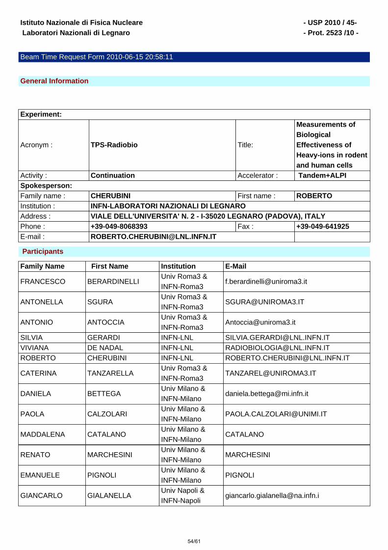
Istituto Nazionale di Fisica Nucleare Laboratori Nazionali di Legnaro
- USP 2010 / 45- - Prot. 2523 /10 -
Beam Time Request Form 2010-06-15 20:58:11
General Information
Experiment:
Acronym : TPS-Radiobio Title:
Measurements ofBiologicalEffectiveness ofHeavy-ions in rodentand human cells
Activity : Continuation Accelerator : Tandem+ALPI Spokesperson: Family name : CHERUBINI First name : ROBERTOInstitution : INFN-LABORATORI NAZIONALI DI LEGNARO Address : VIALE DELL'UNIVERSITA' N. 2 - I-35020 LEGNARO (PADOVA), ITALY Phone : +39-049-8068393 Fax : +39-049-641925 E-mail : [email protected]
Participants
Family Name First Name Institution E-Mail
FRANCESCO BERARDINELLIUniv Roma3 &INFN-Roma3
ANTONELLA SGURAUniv Roma3 &INFN-Roma3
ANTONIO ANTOCCIAUniv Roma3 &INFN-Roma3
SILVIA GERARDI INFN-LNL [email protected] DE NADAL INFN-LNL [email protected] CHERUBINI INFN-LNL [email protected]
CATERINA TANZARELLAUniv Roma3 &INFN-Roma3
DANIELA BETTEGAUniv Milano &INFN-Milano
PAOLA CALZOLARIUniv Milano &INFN-Milano
MADDALENA CATALANOUniv Milano &INFN-Milano
CATALANO
RENATO MARCHESINIUniv Milano &INFN-Milano
MARCHESINI
EMANUELE PIGNOLIUniv Milano &INFN-Milano
PIGNOLI
GIANCARLO GIALANELLAUniv Napoli &INFN-Napoli
54/61
GIANFRANCO GROSSIUniv Napoli &INFN-Napoli
ILARIA IMPROTAUniv Napoli &INFN-Napoli
IMPROTA
LORENZO MANTIUniv Napoli &INFN-Napoli
MANTI
RITA MASSAUniv Napoli &INFN-Napoli
MASSA
PAOLA SCAMPOLIUniv Napoli &INFN-Napoli
Beams Characteristics
Ion Energy[MeV]
Intensity[pnA] Beam Channel Target ExperimentalSetup
Others... 240 20 Continuous +60 Detectors/Biological RadiobiologyOthers... 100/ 20 Continuous +60 Detectors/Biological RadiobiologyOther Ion specification Pulsed Beam Requirements
Requested Beam Time
Run No. of Days Preferred PeriodAbsolutely undesiredperiod
1 2October; Nov. 8-21; Dec17-19;Jan 1-11
2 1October; Nov. 8-21; Dec17-19;Jan 1-11
3 1October; Nov. 8-21; Dec17-19;Jan 1-11
Tot. 4
Sended abstract file: alpi_TPS-Radiobio_1Ab_Proposal TPS-Radiobiologia -Tandem-ALPI_June_2010 Abstract.pdf
Sended proposal file:alpi_TPS-Radiobio_2Pr_Proposal TPS-Radiobiologia -Tandem-ALPI_June_2010.pdf
55/61
TPS-Radiobio Experiment Period: October 2010 – March 2011
Measurements of Biological Effectiveness of Heavy-ions in rodent and human cells
(acronym: TPS-Radiobio)
List of Participants: Roberto CHERUBINI, Viviana DE NADAL, Silvia GERARDI INFN-Laboratori Nazionali di Legnaro, Legnaro-Padova, Italy Antonio ANTOCCIA, Francesco BERARDINELLI, Antonella SGURA, Caterina TANZARELLA Dip. Biologia – Università di Roma3 and INFN-Roma3, Roma, Italy Daniela BETTEGA, Paola CALZOLARI, Maddalena CATALANO, Renato MARCHESINI, Emanuele PIGNOLI Dip. Fisica, Università di Milano and INFN-Milano, Milano, Italy Giancarlo GIALANELLA, Gianfranco GROSSI, Ilaria IMPROTA, Lorenzo MANTI, Rita MASSA, Paola SCAMPOLI Dip. Fisica, Università di Napoli “Federico II” and INFN-Napoli, Napoli, Italy Abstract: The proposed measurements are intended to provide a reliable and coherent set of experimental data on the response of various human normal (healthy) and tumoral cells to Carbon- and lighter ions, as a function of energy and dose, to validate and to contribute to further development of radiobiological models to be used in hadrontherapy application. In particular, in the framework of the INFN strategic project “TPS” (Agodi et al. Nuovo Cimento 31(2008)99-108), aimed at the development of hadrontherapy treatment planning system (TPS), the foreseen experimental radiobiological data will be compared with the simulation results gathered by using the Local Effect Model (LEM; Scholz M. and Kraft G., Adv Space Res 18(1996)5-14), currently used in the commercially available Carbon-ion therapy treatment planning system. TPS is a multi-task project where the Radiobiology task involves four INFN Groups: INFN-LNL, Roma3, Milano, Napoli. In particular the Groups from Milano and Napoli address the study of the radiosensibilization of gliomas for hadron-therapy by means of the addition of the alkilating agent temozolomide (TMZ) before irradiation. These two Groups joined the INFN-LNL and Roma3 Groups in the measurement programme at Tandem-ALPI accelerators in the run of November 10, 2009. Preliminary results obtained at the Tandem-ALPI facility by the Collaboration in the second semester of 2009 are reported.
56/61

TPS-Radiobio Experiment Period: October 2010 – March 2011
Measurements of Biological Effectiveness of Heavy-ions in rodent and human cells
(acronym: TPS-Radiobio)
List of Participants: Roberto CHERUBINI, Viviana DE NADAL, Silvia GERARDI INFN-Laboratori Nazionali di Legnaro, Legnaro-Padova, Italy Antonio ANTOCCIA, Francesco BERARDINELLI, Antonella SGURA, Caterina TANZARELLA Dip. Biologia – Università di Roma3 and INFN-Roma3, Roma, Italy Daniela BETTEGA, Paola CALZOLARI, Maddalena CATALANO, Renato MARCHESINI, Emanuele PIGNOLI Dip. Fisica, Università di Milano and INFN-Milano, Milano, Italy Giancarlo GIALANELLA, Gianfranco GROSSI, Ilaria IMPROTA, Lorenzo MANTI, Rita MASSA, Paola SCAMPOLI Dip. Fisica, Università di Napoli “Federico II” and INFN-Napoli, Napoli, Italy Abstract: The proposed measurements are intended to provide a reliable and coherent set of experimental data on the response of various human normal (healthy) and tumoral cells to Carbon- and lighter ions, as a function of energy and dose, to validate and to contribute to further development of radiobiological models to be used in hadrontherapy application. In particular, in the framework of the INFN strategic project “TPS” (Agodi et al. Nuovo Cimento 31(2008)99-108), aimed at the development of hadrontherapy treatment planning system (TPS), the foreseen experimental radiobiological data will be compared with the simulation results gathered by using the Local Effect Model (LEM; Scholz M. and Kraft G., Adv Space Res 18(1996)5-14), currently used in the commercially available Carbon-ion therapy treatment planning system. TPS is a multi-task project where the Radiobiology task involves four INFN Groups: INFN-LNL, Roma3, Milano, Napoli. In particular the Groups from Milano and Napoli address the study of the radiosensibilization of gliomas for hadron-therapy by means of the addition of the alkilating agent temozolomide (TMZ) before irradiation. These two Groups joined the INFN-LNL and Roma3 Groups in the measurement programme at Tandem-ALPI accelerators in the run of November 10, 2009. Preliminary results obtained at the Tandem-ALPI facility by the Collaboration in the second semester of 2009 are reported.
57/61
TPS-Radiobio Experiment Period: October 2010 – March 2011
Scientific Motivation The main aim of any radiobiology-based TPS for ion therapy (hadrontherapy) is the physical dose optimization inside the tumour and in the irradiated volume, which include also healthy tissues and critical sites/organs near the tumour that need to be spared as much as possible from irradiation, taking profit of the inverted dose profile of charged particles and of the enhanced “Relative Biological Effectiveness” (RBE). In particular, high-LET heavy ions, compared to photons, show physical as well as radiobiological advantages for the treatment of radioresistant tumours (like, for example, glioblastoma tumours). It has been shown that the RBE has a complex dependence on various physical (particle type, energy) and biological (tissue type) factors and it is not univocally defined (depending on the expression level of the biological end-point considered). Therefore a RBE map should be measured for each ion-energy, ion-species (primary and secondary ions) and for every tissue in order to be available for every specific hadrontherapy treatment. This is an experimentally difficult and time-consuming task and for this reason it is necessary to rely on a radiobiological model to predict the RBE for any tissue over a wide range of ion energy and atomic number, taking into account also the mixed radiation field generated through fragmentation of therapeutic carbon ion beams. In the framework of the above mentioned INFN TPS project (Agodi et al. Nuovo Cimento 31(2008)99-108), the Local Effect Model (LEM; Scholz M. and Kraft G., Adv Space Res 18(1996)5-14) has been planned as the baseline for the development of the “TPS”. A systematic radiobiological investigation in terms of cell survival vs. dose (survival curves) in different human cell types (normal and tumoral, with different radiosensitivity) by ion beams of different quality has been planned in order to obtain radiobiological survival curve parameters (α and β values, α/β ratio, RBE) and fill in a database to be used in the TPS. In particular, the selected panel of human cell lines is: AG1522 cells, human normal foreskin fibroblasts; CCD37Lu cells, human normal lung fibroblasts; HSG cells, human salivary gland adenocarcinoma cells; T98G cells, human glioblastoma cells. In addition to human cell lines, as a biological reference system will be also used rodent cells, Chinese hamster V79 cells, which are widely used in ionizing radiation cell survival studies: this is a radio-resistant (repair proficient) cell line and is considered as a reference cell system due to its cellular radiation response, highly reproducible and radiation-quality/LET selective. Glioblastoma multiforme is one of the most aggressive cancers. It shows marked radioresistance and the associated prognosis is very poor. In recently published studies it has been shown that addition of the alkylating agent temozolomide (TMZ) to conventional radiation therapy improves patient survival. Therefore one of the tasks of TPS-Radiobio project, specifically in charge to the Groups of Milano and Napoli, is to evaluate in vitro cytotoxicity (in terms of cell killing) by carbon ions, alone or combined with TMZ, in selected four human glioblastoma cell lines: LN229 , T98G, U87 and U373. Moreover, also other biological end-points turn relevant to be investigated after irradiation of normal and tumour human cell lines, in order to assess the success of the ion treatment as well as the short- and long-term effects due to unwanted irradiation of healthy tissues. Among all, in the present project, the induction of micronuclei, chromosome alteration, DNA damage and its repair will be investigate by the Groups of LNL and Roma3 to build a dose-response curve and derive a measure of the radiosensitivity.
58/61
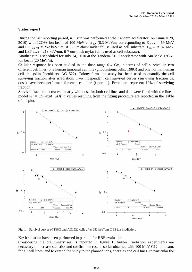
TPS-Radiobio Experiment Period: October 2010 – March 2011
Status report During the last reporting period, n. 1 run was performed at the Tandem accelerator (on January 29, 2010) with 12C6+ ion beam of 100 MeV energy (8.3 MeV/n; corresponding to Eon cell = 69 MeV and LETon cell = 252 keV/um, if 52 um-thick mylar foil is used as cell substrate; Eon cell = 82 MeV and LETon cell = 218 keV/um, if 7 um-thick mylar foil is used as cell substrate). Another run is scheduled for July 24, 2010 at the Tandem-ALPI accelerator with 240 MeV 12C6+ ion beam (20 MeV/n). Cellular response has been studied in the dose range 0-4 Gy, in terms of cell survival in two different cell lines, one human tumoural cell line (glioblastoma cells, T98G) and one normal human cell line (skin fibroblasts, AG1522). Colony-formation assay has been used to quantify the cell surviving fraction after irradiation. Two independent cell survival curves (surviving fraction vs. dose) have been performed for each cell line (figure 1). Error bars represent 10% of surviving fraction. Survival fraction decreases linearly with dose for both cell lines and data were fitted with the linear model SF = SF0 exp[−αD]; α values resulting from the fitting procedure are reported in the Table of the plot. Fig. 1 – Survival curves of T98G and AG1522 cells after 252 keV/um C-12 ion irradiation.
X/γ-irradiation have been performed in parallel for RBE evaluation. Considering the preliminary results reported in figure 1, further irradiation experiments are necessary to increase statistics and confirm the results so far obtained with 100 MeV C12 ion beam, for all cell lines, and to extend the study to the planned ions, energies and cell lines. In particular the
0 1 20,01
0,1
1 AG1522 (I) - C-12 (252 keV/um)
SF
dose (Gy)
Equation y = exp(-alfa*x)Adj. R-Square 0,99979
Value Standard Errorv norm fit alfa 1,78229 0,07668
0 1 20,01
0,1
1 AG01522 (II) - C-12 (252 keV/um)
SF
dose (Gy)
Equation y = exp(-alfa*x)Adj. R-Square 0,9999
Value Standard Errorv norm fit alfa 1,12255 0,02527
0 1 2 3 40,01
0,1
1 T98G (I) - C12 (252 keV/um)
SF
dose (Gy)
Equation y = exp(-alfa*x)Adj. R-Square 0,994
Value Standard ErrorSF n alfa 0,90222 0,11769
0 1 2 30,01
0,1
1 T98G (II) - C12 (252 keV/um)
SF
dose (Gy)
Equation y = exp(-alfa*x)Adj. R-Square 0,99696
Value Standard Errorv norm fit alfa 0,97679 0,06818
59/61

TPS-Radiobio Experiment Period: October 2010 – March 2011
investigation with 100 MeV C12 beam will be extended also to HSG (Human Salivary Gland) tumour cells. As regards measurements dedicated to the investigation of radiosensibilization of gliomas, preliminary results obtained for carbon ions (two experiments at LNL, 8.3 MeV/n, 218 keV/μm) and, for comparison, for X rays (see Fig 2) indicate that high-LET carbon ions inactivate much more effectively than X-rays the proliferative capacity of all the investigated glioblastoma cell – lines (LN229 , T98G, U87 and U373). The effect of TMZ addition to carbon ions irradiation is shown in Fig. 3. The results are still preliminary and more experiments are necessary to clarify how TMZ interacts with the carbon ions irradiation .
Fig. 2 – Dose-response of LN229, U373,T98G and U87-MG cells to 218 keV/μm C-ions and X-rays .
0 2 4 6 8
0,01
0,1
1 U373 cells
218 keV/μm C-ions 6 MeV photons
Surv
ivin
g fra
ctio
n
Dose ( Gy )
0 2 4 6 8
0,01
0,1
1 LN229 cells
218 keV/μm C-ions 6 MeV photons
Sur
vivi
ng fr
actio
n
Dose ( Gy )
0 2 4 6 8
0,01
0,1
1 T98 cells
6 MeV photons 218 keV/μm C-ions
Surv
ivin
g fra
ctio
n
Dose ( Gy)0 2 4 6 8
0,01
0,1
1
U 87-MG cells
218 keV/μm C-ions X-rays
Surv
ivin
g fra
ctio
n
Dose ( Gy )
60/61

TPS-Radiobio Experiment Period: October 2010 – March 2011
Fig. 3 – Dose-response of LN229, U373,T98G and U87-MG cells to 218 keV/μm C-ions +/- TMZ Beam-time requests and measurements In the period of reference October 2010 – March 2011, n. 3 runs of 4 days in total, in three independent runs, are requested to continue the study of cellular response in the selected panel normal and tumoural cell lines of different radiosensitivity (AG1522, T98G, HSG), in the reference rodent V79 cells, and in glioma cell lines (LN229, T98G, U87 and U373) with and without TMZ, as a function of the dose, in the range 0-8 Gy.
In particular, the beam-time request is:
n. 1 run of 2 days at the Tandem-Alpi accelerator complex; 12C6+, 20 MeV/n n. 2 runs of 1 day each at the Tandem accelerator; 12C6+, 100 MeV
During the requested runs, physical and dosimetric ion beam characterization will be also performed.
In parallel to ion irradiations, experiments will be performed by using X- and gamma-rays at the different home-laboratories of the involved Groups.
0 2 40,01
0,1
1 LN229 cells
218 keV/ μm C-ions 218 keV/ μm C-ions +20μM TMZ
Surv
ivin
g fra
ctio
n
Dose ( Gy )0 2 4
0,01
0,1
1
U373 cells 218 keV/μm C-ions 218 keV/μm C-ions + 50μM TMZ
Surv
ivin
g fra
ctio
n
Dose ( Gy )
0 2 40,01
0,1
1T98G cells
218 keV/μm C-ions 218 keV/μm C-ions + 50μM TMZ
Sur
vivi
ng fr
actio
n
Dose ( Gy ) 0 2 40,01
0,1
1 U 87-MG cells 218 keV/μm C-ions 218 keV/μm C-ions+50μM TMZ
Sur
vivi
ng fr
actio
n
Dose ( Gy )
61/61