explain the introduction to adc, adc characteristics, programming adc using pic18, introduction to...
TRANSCRIPT

Explain the introduction to ADC, ADC characteristics, Programming ADC using PIC18, Introduction to DAC and DAC interfacing with PIC18.

Discuss the ADC of the PIC18Explain the process of data
acquisition using ADCProgram the PIC18’s ADC in
assemblyDescribe the basic operation of DAC Interface a DAC chip to the PIC18
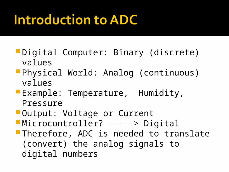
Digital Computer: Binary (discrete) values Physical World: Analog (continuous)
values Example: Temperature, Humidity,
Pressure Output: Voltage or Current Microcontroller? -----> Digital Therefore, ADC is needed to translate
(convert) the analog signals to digital numbers

Microcontroller Connection to Sensor via ADC

n-bit No. of steps Step size (mV)
8 28 = 256 5/256 = 19.53
10 210 = 1024 5/1024 = 4.88
12 212 = 4096 5/4096 = 1.2
Assuming VREF = 5V
* Step Size (Resolution): is the smallest change that can be discerned by an ADC

Vref: Input voltage used for the reference voltage
The voltage connected to this pin , with the resolution of the ADC chip, dictate the step size
Example: If we need the analog input to be 0 to 4 volts, Vref is connected to 4 volts
Digital data output: 8-bit (D0-D7), 10-bit (D0-D9)

Vref (V) Vin (V) Step size (mV)
5.00 0 to 5 5/1024 = 4.88
4.096 0 to 4.096 4.096/1024 = 4
3.0 0 to 3 3/1024 = 2.93
2.56 0 to 2.56 2.56/1024 = 2.5
2.048 0 to 2.048 2.048/1024 = 2
Vref Relation to Vin Range for an 10-bit ADC

Dout = Vin / Step Size
Digital data output (in decimal):
8-bit (D0-D7)= 25610-bit (D0-D9) = 1024
Analog Input Voltage
Example:Vref = 2.56, Vin = 1.7V.Calculate the Do-D9 output?
Solution:Step Size = 2.56/1024 = 2.5mVDout = 1.7/2.5mV = 680 (Decimal)D0-D9 = 1010101000


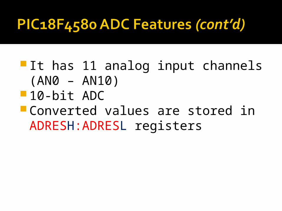
It has 11 analog input channels (AN0 – AN10)
10-bit ADCConverted values are stored in
ADRESH:ADRESL registers

A/D Control Register 0 (ADCON0) Controls the operation of the A/D module
A/D Control Register 1 (ADCON1) Configures the functions of the port pins
A/D Control Register 2 (ADCON2) Configures the A/D clock source,
programmed acquisition time and justification

Different from the Book!
Example:
ADCON0 = 00101001

* Different from the Book!

Example:
ADCON1 = 00001110
* Different from the Book!

* Different from the Book!
Example:
ADCON2 = 10000110

ADFM Bit and ADRESx Registers

For a PIC18-based system, we have Vref = Vdd = 5V. Find a) The step size and b) The ADCON1 value if we need 3 channels.
a)The step size = 5/1024 = 4,8mVb)ADCON1 = 00001100

Define in term of Tad (Conversion time per bit)
To calculate: FOSC/2, FOSC/4, FOSC/8, FOSC/16, FOSC/32 or FOSC/64

TURN ON the ADC module (BSF ADCON0, ADON)
Make the ADC channel pin as input pin Select voltage reference and ADC channel Select the conversion speed Wait for the required acquisition time Activate the start conversion bit of
GO/DONE Wait for the conversion to be completed
by pooling the end-of-conversion GO/DONE bit
After the GO/DONE bit has gone LOW, read the ADRESL and ADRESH register

ORG 0000HCLRF TRISCCLRF TRISDBSF TRISA, 0MOVLW 0x00MOVWF ADCON0MOVLW 0x0EMOVWF ADCON1MOVLW 0xBEMOVWF ADCON2
OV ER CALL DELAYBSF ADCON0, GO
BACK BTFS ADCON0, GONEBRA BACKMOVFF ADRESL,
PORTCMOVFF ADRESH,
PORTDCALL QSEC_DELAYBRA OVEREND

Interrupt
Flag Bit Register Enable Bit
Register
ADIF (ADC)
ADIF PIR1 ADIE PIE1
ADC Interrupt Flag Bits and Associated Registers
* Please see Program 13-2 page 514
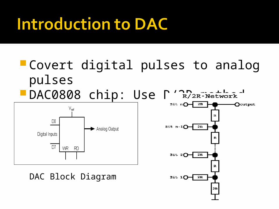
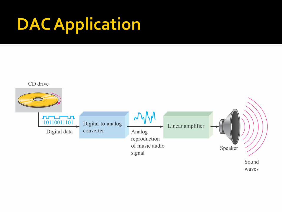
Covert digital pulses to analog pulses
DAC0808 chip: Use R/2R method, 8-bit
DAC Block Diagram
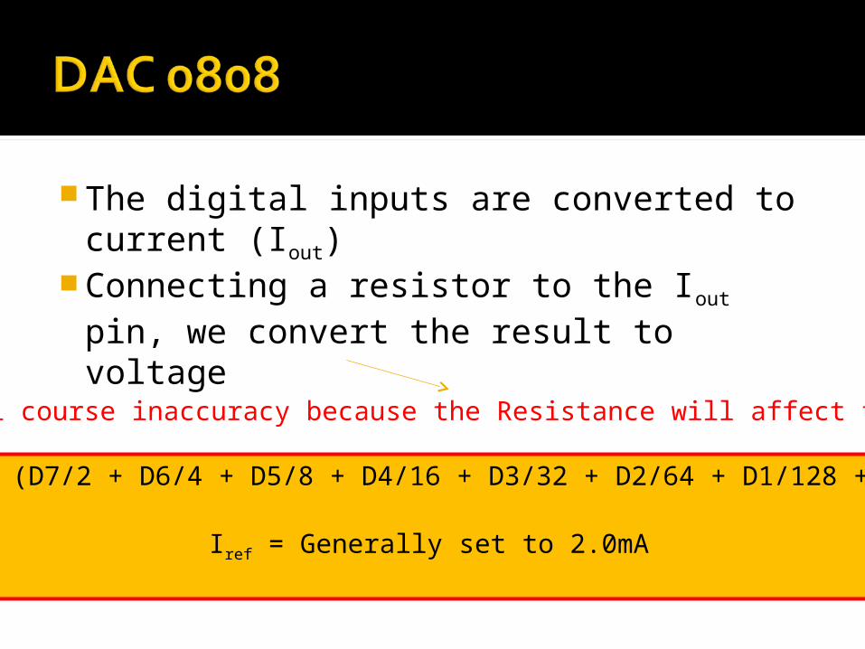
The digital inputs are converted to current (Iout)
Connecting a resistor to the Iout pin, we convert the result to voltage
Iout = Iref (D7/2 + D6/4 + D5/8 + D4/16 + D3/32 + D2/64 + D1/128 + D0/256)
Iref = Generally set to 2.0mA
This will course inaccuracy because the Resistance will affect the reading

Example:
Binary input: 10011001Iout = 2mA (153/256) = 1.195mA
and
Vout = 1.195mA x 5K = 5.975V
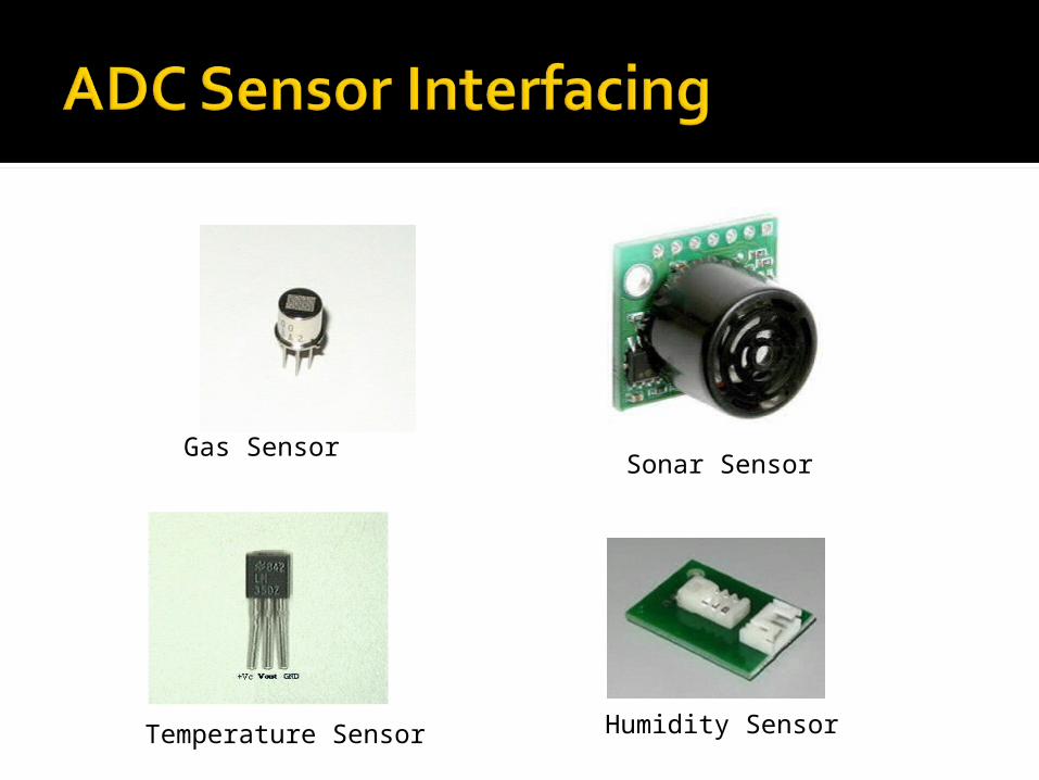
Gas Sensor
Temperature Sensor Humidity Sensor
Sonar Sensor

Characteristic:
1)Precision integrated-circuit2)Output voltage is linearly proportional to the Celcius3)Requires no external calibration (Internally calibration)4)Output: 10mV for each degree

10mV = 1 degree (Minimum)20mV = 2 degree30mV = 3 degree....1000mV = 100 degree (Maximum)
Vref = ???
5V
1.024
Step Size = 4.8mV
Step Size = 1mV
Vin (max) = 5V
Vin (max)
= 1.024V
Which one suitable?
How to set
Vref??

To overcome any fluctuations in power supply.
* Please see Program 13-4 page 524

“Things are only impossible until they're not”