exploring the use of diamond in medical implants
TRANSCRIPT

ii
EXPLORING THE USE OF DIAMOND IN MEDICAL
IMPLANTS
Md. Kabir Uddin Sikder
https://orcid.org/0000-0001-8930-7209
A thesis for the fulfillment of
Doctor of Philosophy
October 2018
Department of Medical Bionics
(Bionics Institute)
Faculty of Medicine, Dentistry and Health Sciences
The University of Melbourne
Parkville, Victoria 3010
Australia

iii
Thesis abstract
Over recent decades, there is increasing interest in implantable devices that interact with
neural tissue in the human body. Applications are broad, ranging from cardiac
pacemakers to cochlear implants and beyond. The emergence of microelectronics and
microfabrication has led to the miniaturization of these neural implants. Small devices
are safer to implant but a number of challenges need to be addressed before very small
devices are routinely deployed.
For instance, it is difficult to transfer sufficient power to small implants wirelessly, and
difficult to fabricate small neurostimulation microelectrodes with high enough charge
injection capacity to operate safely. Compounding this, the immune system of the body
can react to the implant. Unfavourable interactions of the electrode with tissue/neurons
leads to a sharp drop in performance caused by scar tissue surrounding them. These
challenges, among others, must be overcome in order to reduce the size of implants into
the low millimeter dimensions. Devices at this scale will be insertable with minimal
trauma and will hence be deployable in a greater range of circumstances. Here we
investigate the use of diamond as a biomaterial with the potential to mitigate or
ameliorate some of these challenges.
In this work, a novel technique for microcoil fabrication is introduced. Trenches were
milled into a diamond substrate and filled with silver active braze alloy, enabling the
manufacture of small, high cross-section, low impedance microcoils capable of wireless
power transmission of 10 mW over 6 mm. The coils were encapsulated in a second
layer of diamond, characterized, and accelerated ageing was performed to verify the
longevity of the construct.

iv
Building on previous work, a method was developed to grow conducting diamond films
on platinum foil. A laser roughening method was used to increase adhesion of the
diamond to the platinum. This approach enables the superior properties of diamond to
be integrated into devices constructed using traditional fabrication methods such as wire
bonding or laser welding. Laser roughened platinum was coated with nitrogen induced
ultra-nanocrystalline diamond (N-UNCD) films and the electrochemical performance of
these films was measured relative to platinum. Stronger attachment of N-UNCD to
platinum substrates of higher roughness was observed. Diamond on platinum electrodes
were found to be more capacitive and stable compared to platinum controls, a favorable
characteristic for neural stimulation.
Finally, an extracellular matrix protein (laminin) known to be involved in inter-neuron
adhesion and recognition, was covalently coupled to diamond electrodes. Biologically,
active interlayers have the potential to increase neural adhesion to electrodes and/or
reduce the immune response, thus increasing longevity. Electrochemical analysis found
that covalently coupled films were robust and resulted in minimal change to
electrochemical properties of the electrodes. Neurons cultured on laminin coated
surfaces exhibited improved adhesion.
This thesis demonstrates that diamond is a versatile material for use in medical
implants. It can be used as a construction material and as an encapsulant containing
electrically active elements. It can be made electrically conductive and possesses
suitable electrochemical properties for neural stimulation. Finally, it can be employed as
a chemically active substrate for attachment of additional chemistries, including
biomolecules.

v
Date: 05/10/2018
Declaration
i) The thesis comprises only my original work towards the degree of Doctor of Philosophy
except where indicated in the preface
ii) Due acknowledgment has been made in the text to all other material used; and
iii) The thesis is fewer than the maximum word limit (100,000) in length, exclusive of
tables, maps, bibliographies, and appendices or that the thesis is (34,204) as approved
by the Research Higher Degrees Committee.
The necessary permission from co-authors of my own published work in peer-reviewed
journals has been taken to reproduce in the thesis. Research for this thesis was mainly
carried out at the Department of Physics, the University of Melbourne, Bionics Institute
and National Vision Research Institute, Melbourne, Australia.
(Md. Kabir Uddin Sikder)
Signature of candidate

vi
Preface
The work presented in this thesis is multidisciplinary in nature, and thus, required
expertise in different fields to be performed to a high scientific standard. Therefore, the
author relied on collaborations/ training with different experts whose contributions are
acknowledged below. The cell culture on diamond film to assess the cell adhesion
presented in Chapter - 4, was performed by Wei Tong. The author of this thesis
deposited and prepared the diamond samples for cell culture. The author also performed
the imaging of cells, data collection, and analysis to prepare the final results of cell
culture experiment. X-ray photoelectron spectroscopy was performed by Hitesh Pingle
and data analysis was revised by Peter Kingshott. David J. Garrett, Mohit Shivdasani,
James B. Fallon, and Peter Seligman supported the author to design the experiments as
supervisors. Kumaravelu Ganesan trained the author to perform various experiments
during his candidature.
This research and KS were supported by an Australian Research Council (ARC)
DECRA grant DE130100922. DJG is supported by the National Health and Medical
Research Council (NHMRC) of Australia, grant GNT1101717. MNS is supported by
the National Health and Medical Research Council (NHMRC) of Australia, grant
GNT1063093. The Bionics Institute acknowledges the support received from the
Victorian Government through its Operational Infrastructure Program for this work.
Md. Kabir Uddin Sikder

vii
Acknowledgments
Firstly, I acknowledge the potential supervisions and proper guidance of my supervisors
who made this work possible by me. I am thankful for their patience and all fruitful
advice for research planning during the candidature period. In the rest of my life always
I will be guided by their amazing art of analytical and critical debate on research topics
in the progress review meetings which they taught me for a deeper understanding of the
present work in this thesis. I am extremely thankful to them for having the lessons and
acknowledge their teachings.
I would like to acknowledge the quality of support in every aspect of my principal
supervisor David J. Garrett to complete this thesis. I especially thank him for the major
training in the Department of Physics, the University of Melbourne to perform my
research work. Thanks to James B. Fallon, Mohit Shivdasani and Prof. Peter Seligman
for monitoring my progress and oversight of my research. I thank Mohit Shivdasani and
Prof. Peter Seligman to train me to use the laboratory equipment at Bionics Institute. I
thank David J. Garrett and the rest of my supervisors to edit the manuscripts and their
wise words to express the work properly.
I am highly thankful to Karina Needham and Wei Tong to perform cell culture and
relevant experiments. Kumaravelu Ganesan is one of the key personnel in the
Department of Physics, the University of Melbourne who trained me to use materials
laboratory and clean room there. He taught me so many little-little things which became
very important to carry out my research as they were not available anywhere except

viii
experience. I thank him so much and the same for Rodney Millard and Vanessa Maxim
at Bionics Institute for their cordial cooperation all the time of my candidature.
Thanks to Joel Villalobos, Rachael Richardson, Nick Apollo, Arman Anood, Athavan
Nadarajah, and Chris Williams for their valuable time for me willing to listen and
discuss. Thanks, Owen Burns, Thomas Ross, Andrew Purnama, Ceara McGowan,
Stephanie Epp for their technical support. Thanks to my colleagues and friends, Thomas
Spencer, Sam Titchener, Yuri Benovitski and others.
I would also like to thank the Bionics Institute and National Vision Research Institute
(NVRI), Bio21 and the Florey Institute of Mental Health for the provision of
experimental facilities. I also extend my thanks to the anonymous reviewers of the
papers included in this thesis whose contribution has been invaluable.
A thank my family members, especially my mother Mahfuza Begum who have not seen
me over the years for the Ph.D. program, for their support and encouragement. Finally,
but most importantly to my wife Mst. Salma Pervin who has sacrificed much of her
time, energy and herself toward my studies. Also, my children Saif Uddin and Saadia
who missed me in the most of their time. Thank you all for letting me work late and
your patience. Your support and encouragement during my Ph.D. were a real blessing.

ix
Thesis style
The Higher Degrees Committee (Research) of the University of Melbourne permits
thesis submission by published and unpublished papers as an alternative to the
conventional thesis format. Thus, I decided to present the thesis as a series of papers.
The thesis has three sections: Background and Literature Review (chapter 1),
Experimental work arranged as published and unpublished papers (chapter 2-4) and
General Discussions and Conclusions (Chapter 5). Chapter 2 has been published in the
Journal of Biomedical Microdevices entitled ‘Wireless induction coils embedded in
diamond for power transfer in medical implant’. Chapter 3 and Chapter 4 are in
preparation for publication.

x
Thesis overview
CHAPTER 1: Background and General Literature Review
A general overview on inductive power transfer systems, electrode materials and their
electrochemical properties and biomolecular coating on electrodes as well as research
problems have been described in this chapter.
CHAPTER 2: Wireless Inductive Coils Embedded in Diamond for Power
Transfer in Medical Implants
The design, fabrication, electrical characterization of microcoils and their long-term
functionality through being hermetically encapsulated in diamond have been described
in this chapter.
Aims:
i) To make embedded microcoils in diamond, manipulating their shape and
geometrical dimensions to evaluate their inductive power transfer efficiency.
ii) To establish how a metallic braze line for hermetic sealing impacts on power
transfer efficiency of the adjacent microcoils.
iii) To develop a method to grow diamond over embedded coils encapsulating
them and permitting the use of non-biocompatible metals such as silver or
silver alloys.

xi
CHAPTER 3: Diamond Coating Improves the Electrochemical
Characteristics of Platinum Electrodes
Fabrication of functional electrodes of platinum roughened platinum and nitrogen
introduced ultra-nanocrystalline diamond (N-UNCD) grown on roughened platinum
foils. Electrochemical characterizations of electrodes using standard electrochemical
techniques is presented. Mechanical, electrical and electrochemical stability assessments
of the electrodes are described.
Aims:
i) To develop N-UNCD films grown on laser roughened platinum (Pt) foil.
ii) To evaluate the mechanical and electrochemical stability of N-UNCD
compared to conventional electrode materials.
iii) To evaluate and compare N-UNCD electrodes with other electrode materials
(platinum and roughened platinum) using standard electrochemical
techniques.
CHAPTER 4: Protein Coating Improves Neural Adhesion on Diamond
Films Preserving Electrochemical Properties
Extracellular matrix protein (laminin) coating by electrochemical and chemical methods
on N-UNCD films grown on roughened platinum is described. Electrochemical
characterization of laminin-coated N-UNCD electrodes and the stability of the laminin
layer onto N-UNCD electrodes are presented.

xii
Aims:
i) To couple laminin onto N-UNCD films through an electrochemical process.
ii) To establish the impact of covalently coupled films on the electrochemical
properties of N-UNCD electrodes.
iii) To evaluate electrochemical stability of covalently coupled laminin layer on
N-UNCD electrodes.
iv) In vitro biocompatibility assessment through neuronal cell adhesion and
neurite growth analysis
CHAPTER 5: General Discussions and Conclusions
Discussion of the major research outcomes of the work, potential applications, and
future work.

xiii
Table of Contents
Page
Thesis abstract …………………………………………………….. ii
Declaration …………………………………………...…………… iv
Preface …………………………………………………………….. v
Acknowledgements ………………………………………………. vi
Thesis style ……………………………………………………… viii
Thesis overview ………………………………………………… . ix
Table of contents …………………………………………………. xii
List of tables ……………………………………………………… xviii
List of figures ……………………………………………………… xix
List of abbreviations ……………………………………………… xxv
CHAPTER 1 30
Background and General Literature Review 30
1.1 Wireless power transmission and hermetic packaging ………………… 31
1.1.1 Power delivery approaches …………………………………… 31
1.1.2 Hermetic packaging of medical implants……………………… 37
1.2 Electrode materials for neural stimulation ……………………………… 38

xiv
1.2.1 A brief history of neural stimulation ………………………… 38
1.2.2 Electrochemistry of stimulation electrodes …………………… 43
1.2.2.1 Charge transfer process of electrode materials ……… 44
1.2.2.2 Charge injection capacity …………………………… 46
1.2.2.3 Electrochemical impedance ………………………… 48
1.2.3 Miniaturization of electrodes for neural prosthesis …………… 49
1.2.4 Historical progression and emergence of new electrode
materials ………………………………………………………. 50
1.3 Biomolecular coating on electrode surface ………………………………. 55
1.3.1 Electrode tissue interaction …………………………………… 55
1.3.2 Biomolecules for coating ………………………………………. 56
1.4 Diamond is the material of choice in this study ………………………….. 60
CHAPTER 2 62
Wireless Inductive Coils Embedded in Diamond for Power
Transfer in Medical Implants 62
2.1 Introduction …………………………………………………………… 64
2.2 Materials and methods .……………………………………………….. 68
2.2.1 Materials ………………………………………………………... 68

xv
2.2.2 Design and fabrication method of microcoils embedded in diamond 69
2.2.3 Electrical characterization method ……………………………… 70
2.2.4 Wireless power transfer and braze line effect measurement method 71
2.2.5 Coil encapsulation method ………………………………………. 72
2.2.6 Accelerated ageing method ……………………………………… 73
2.3 Results and discussions …………………………………………………….. 73
2.3.1 Microcoil fabrication outcomes ………………………………….. 73
2.3.2 Electrical characterization ………………………………………... 76
2.3.3 Wireless power transfer and braze line effects …………………… 76
2.3.4 Effects of encapsulation and accelerated ageing …………………... 78
2.4 Conclusions ………………………………………………………………….. 83
CHAPTER 3 85
Diamond Coating Improves the Electrochemical Characteristics of
Platinum Electrodes 85
3.1 Introduction ……………………………………………………………… 86
3.2 Materials and methods …………………………………………………... 90
3.2.1 Materials and equipment ……………………………………… 90
3.2.2 Nitrogen induced ultra-nanocrystalline diamond (N-UNCD) film

xvi
deposition ……………………………………………………… 91
3.2.3 Mechanical stability of N-UNCD films ……………………….. 91
3.2.3.1 Sonication …………………………………………… 91
3.2.3.2 Scratch test ………………………………………….. 92
3.2.4 Design and fabrication of electrodes ………………………….. 92
3.2.5 Electrochemical characterization methods ……………………. 93
3.2.5.1 Cyclic voltammetry …………………………………. 94
3.2.5.2 Electrochemical impedance spectroscopy (EIS) ……. 95
3.2.5.3 Voltage transient measurements …………………… 97
3.2.6 Electrochemical stability assessment of electrodes …………… 99
3.2.7 SEM imaging .………………………………………………… 100
3.3 Results and discussions …………………………………………………. 100
3.3.1 Mechanical stability of N-UNCD films ………………………. 100
3.3.1.1 Sonication …………………………………………... 100
3.3.1.2 Scratch test …………………………………………. 103
3.3.2 Electrochemical characterization ………………………….… 106
3.3.2.1 Cyclic voltammetry measurements ………………… 106
3.3.2.2 EIS, 1 kHz impedance measurements ……………… 108
3.3.2.3 Voltage transient measurements ……………………. 110
3.3.3 Electrochemical stability assessment of electrodes …………… 114

xvii
3.3.3.1 Long-term stimulation of electrodes ………………… 114
3.3.3.3 SEM imaging ………………………………………. 121
3.4 Conclusions …………………………………………………………….. 124
CHAPTER 4 125
Protein Coating Improves Neural Adhesion on Diamond
Films Preserving Electrochemical Properties 125
4.1 Introduction …………………………………………………………… 126
4.2 Materials ……………………………………………………………… 130
4.3 Methods ……………………………………………………………… 132
4.3.1 Ethics details ………………………………………………… 132
4.3.2 N-UNCD film deposition …………………………………… 132
4.3.3 Laminin coating on diamond films ………………………… 132
4.3.4 Assessment of laminin coating ……………………………… 134
4.3.4.1 X-ray photoelectron spectroscopy (XPS) ………… 134
4.3.4.1.1 Thickness of laminin layer …………………….. 134
4.3.4.1.2 Surface coverage of laminin layer ………………… 135
4.3.5 Electrochemical characterization …………………………… 135
4.3.6 Stability assessment of laminin coupling …………………… 136

xviii
4.3.7 Cell adhesion on diamond films …………………………… 136
4.3.7.1 Primary rat cortical neuron culture ………………… 136
4.3.7.2 Fixation and immunostaining of cells …………… 137
4.3.7.3 Microscope imaging ……………………………… 138
4.4 Results and discussions ……………………………………………… 138
4.4.1 Assessment of laminin coating …………………………… 138
4.4.1.1 XPS analysis …………………………………… 139
4.4.2 Electrochemical characterization ………………………… 145
4.4.3 Stability of laminin coupling .…………………………… 152
4.4.4 Cell adhesion on diamond films ………………………… 153
4.5 Conclusions ………………………………………………………… 155
CHAPTER 5 157
General Discussions and Conclusions 157
5.1 Detailed outcomes of the present work …………………………… 158
5.2 Future work ………………………………………………………… 162
5.3 Conclusions ………………………………………………………… 163
REFERENCES 165

xix
List of tables
Table 1.1 Power delivery capacity of different approaches for medical implants
Table 1.2 A timeline of electrical stimulation
Table 1.3 Charge-injection limits of electrode materials for stimulation
Table 1.4 Combinations of coatings and biomolecules to investigate the improvement
of electrode-neuron interfacing
Table 2.1 Resistance and Q-factor (average ± std. error) of four sets of coils embedded
in diamond with several design parameters. Values in parentheses show
targeted/expected parameters. *Difficulty in getting accurate depth data from this set of
coils
Table 3.1 Assessment of the degree of damage due to scratch test on N-UNCD films
Table 3.2 Degree of damage and/or corrosion of electrode materials
Table 4.1 Percentage of elemental contribution (% ± STD) obtained from XPS on N-
UNCD and N-UNCD-O films during laminin coating process
Table 4.2 Thickness and surface coverage of the laminin layer on diamond films

xx
List of figures
Fig. 1.1 The principle of inductive power transfer describing Faraday’s law.
Fig. 1.2 Concept of the EPI-RET-3 wireless retina implant system.
Fig. 1.3 Drawing of the EPI-RET-3 wireless retina implant.
Fig. 1.4 Image of an adult Nile electric catfish used to treat pain appear in artifacts from
the period of the predynastic Egyptian ruler.
Fig. 1.5 Artist's impression of the use of the electrical torpedo fish in the treatment of
gout (a) and headache (b)
Fig. 1.6 Galvani connects the lumbar nerves to the crural muscle of a frog through a
bimetallic circuit of zinc (z) and copper (c): the leg kicks outwards
Fig. 1.7 Lindstrom's Electro Medical apparatus was widely used in the Midwest USA
around 1894
Fig. 1.8 An implantable single lead pacemaker is about 4 cm long and 3 cm wide. The
electric device consists of two main parts, a thin metal box, and wires. A
generator in the thin box which creates an electrical impulse powered by a
battery. The number of wires varies from one to three which are connected to
the generator and little electrodes for stimulation are placed on their tips
(source: nordcardio.com).
Fig. 1.9 An image of a typical cochlear implant showing its different parts including
stimulation electrodes (source: Med-EL).
Fig. 1.10 Images of stimulation electrode arrays for deep brain stimulation device (A,
source: Medscape), cochlear implant (B, source: MED-EL) and retinal implant
(C).
Fig. 1.11 The interface of electrode and electrolyte, illustrating Faradaic charge transfer
(top) and capacitive redistribution of charge (bottom) as the electrode is
driven negative: (A) physical representation; (B) two-element electrical circuit
model for mechanisms of charge transfer at the interface. The capacitive
process involves reversible redistribution of charge. The Faradaic process
involves a transfer of electrons from the metal electrode, reducing hydrated
cations. Faradaic charge injection may or may not be reversible.
Fig. 1.12 SEM of an AIROF microelectrode pulsed at 3 mC/cm2 for 1600s showing a
fracture of the oxide film.

xxi
Fig. 1.13 A) A flat N-UNCD high-density microelectrode array isolated by laser milling
(left), B) Templated diamond spikes produced by Ganesan et al. (Right).
Fig. 1.14 (a) SEM image of a 200 × 200 mm square N-UNCD electrode that has been
used as a stimulating electrode on excised rat retina. Inset is a micrograph of
the electrode before insulation with epoxy and silicone. (b) An SEM image of
a 600 mm diameter N-UNCD disc electrode used to assess electrochemical
stability. Inset is a micrograph of four such electrodes attached to a flexible
circuit board and isolated with epoxy resin.
Fig. 1.15 Schematic diagram of the extracellular matrix (source: Rose L. Hamm,
McGraw-Hill Education).
Fig. 1.16 Schematic diagram of laminin molecule structure and function (source:
Pearson education. Inc. publishing as Benjamin Cummings, 2003).
Fig. 2.1 The schematic diagram of an embedded coil in a diamond where the coil is
hermetically sealed using laser welding of gold ABA braze lines.
Fig. 2.2 (a) Sequence of microcoil fabrication process, (b) SEM of microcoil trench, (c)
Optical profilometer image of microcoil trenches (bottom of the trench is in blue)
and (d) SEM image of a 4.6 × 4.6 mm coil with 20 turns of silver ABA after
fabrication.
Fig. 2.3 Schematic diagrams: (a) circuit of the transceiver unit, (b) parallel position of
gold braze line to the plane of microcoil and (c) perpendicular position of gold
braze line to the plane of the microcoil.
Fig. 2.4 (a) Top view SEM image of a microcoil from set 4, (b) SEM image of a crack
in PCD between two turns.
Fig. 2.5 (a) Average resistance and (b) Average Q-factor of the eight microcoils from
set 4. X-axes are in log scale.
Fig. 2.6 (a) Transmitted average power and (b) average power efficiency, plotted
against load resistance for the 4.6 mm diameter coils (n=6) described in table
2.1 from set 4 at a distance of 6 mm between the transmitter and receiver coil,
(c) Shows the impact of a parallel gold braze line (5.1 × 5.1 mm) on power
transfer efficiency of the three highest Q-factor microcoils taken from set 4,
The plots show the change in power efficiency (across 0.51 kΩ) of the
microcoils with increasing distance of the braze line, (d) Shows a comparison
of power transfer efficiency for the same three coils as (c) between a braze ring
parallel to the coil and a braze line placed 0.2 mm away from the outer edge in
a perpendicular orientation with respect to without any braze line.
Fig. 2.7 Raman spectra (λ = 532 nm) obtained from the PCD layer on Ag ABA trenches
(spots 1-2) and on diamond islands separating two consecutive turns of the coil
(spots 3-4).
xxii
Fig. 2.8 (a) SEM image (top view) of a microcoil after PCD growth on the exposed
surface, (b) Magnified (1000x) SEM image of the red box in the fig. (a).
Figures c-f show the change in Q-factor for samples before and after PCD
growth, after accelerated aging and after oxygen plasma treatment respectively.
The PCD growth times for the samples were (c) 5 h, (d) & (e) 14 h and (f)
shows the data corresponding to one of the two samples where the silver coil
was aged without PCD growth.
Fig. 2.9 Typical spots for elemental analysis on PCD layer grown on Ag ABA
microcoils after ageing test. A1-A2) Silver peaks of EDS spectrum (A1)
performed on the PCD layer of growth time of 5 h (A2). A3-4) Only the carbon
peak was observed in the EDS spectrum (A3) on the PCD layer grown for 14 h
(A4).
Fig. 3.1 SEM image of diamond film grown for 3 h on smooth Pt foil. The film was
peeled off from the Pt substrate.
Fig. 3.2 Photolithographically fabricated electrodes of Pt (A), rPt (B) and N-UNCD (C)
using su8 2010. The diameter of the electrodes was 1000 µm.
Fig. 3.3 Three-electrode electrochemical cell with O-ring setup. Counter electrode (CE)
was connected with yellow alligator clip and reference electrode (RE) was
connected with black alligator clip shown separately at the right side of the
cell. Sample WE such as NUNCD was kept on copper plate and top of it the O-
ring was placed. N-UNCD and O-ring are separately shown in the left side of
the cell. A glass beaker having a hole at its bottom fixed on the O-ring by
screws in a steel frame such that sample surface was exposed to electrolyte
while it was poured into the beaker. Red alligator clip was connected to
NUNCD electrode through copper plate.
Fig. 3.4 Typical CV for a for a bare electrode in a redox inactive salt solution.
Fig. 3.5 Randles equivalent model circuit. An interfacial charge transfer resistance (Rct)
is connected to a capacitor of double layer capacitance (Cdl) in parallel. A
model resistance Rs instead of solution resistance is connected to RC circuit.
Fig. 3.6 A typical impedance spectrum for N-UNCD electrode of 1000 µm diameter in
0.9% saline
Fig. 3.7 A voltage transient of a microelectrode in response to a biphasic and symmetric
(ic=ia) current pulse. The maximum cathodic polarization Emc = Eipp + ∆Ep =
Eipp + (∆V-Va); where Eipp was interpulse potential, ∆Ep was net potential
difference across electrode-electrolyte, ∆V was the total voltage transient and
Va was access voltage includes concentration overpotential and electrolyte
voltage drop icRi which produces uncertainty in ∆Ep. Ema was maximum anodic
polarization potential [1].
Fig. 3.8 N-UNCD growth on rPt substrates of 4 × 4 mm: The samples in the top SEM
images (A, B, and C, scale bar 100 µm) were for 20 µm, 40 µm, and 80 µm
separations between pits respectively. N-UNCD films of 3 h growth time on
rPt are shown in D, E, and F, (scale bar 50 µm).

xxiii
Fig. 3.9 Microscope images (4x magnification) of N-UNCD films of 3 h growth time on
rPt substrate showing delamination due to sonication. Peeling off the N-UNCD
films from rPt substrates were increased with increasing the lattice distance of
the pits on rPt substrates from column 1 to 3.
Fig. 3.10 A5) N-UNCD film deposited on rPt (pits spacing 20 µm) sonicated for 30 h
and A5a) extended SEM image (800x magnification) of the delaminated area
(white) on image A5.
Fig. 3.11 Image ‘A’ as grown N-UNCD film (scale bar 20 µm). Damage after the
applied force of 0.5 N (B, scale bar 25 µm), 7 N (C, scale bar 20 µm) and 15 N
(D, scale bar 20 µm), and E is an extended view of image B.
Fig. 3.12 Typical representative CV of Pt (n=12), rPt (n=12), N-UNCD (n=11) and N-
UNCD-O (n=3) conducted at 50 mV/s within the water window (-0.6 to 0.8V)
of Pt in 0.9% saline (A). Small CVs’ within a voltage limit of -0.1 to 0.1V were
taken at 10, 20, 30, 40 and 50 mV/s scan rates for test electrode materials and a
typical series of small CVs for N-UNCD (B) is presented here. At 0 V the
magnitude of the difference of positive and negative amplitude of current from
each small CV at each scan rate mentioned in B was extracted and plotted
against their respective scan rates (C). The slope of the plot in C provided the
capacitance of the electrodes. The capacitance times the maximum limit of the
water window provided the total charge on the electrode surface and the charge
per unit area is CSC (D). EIS conducted at 10 mV and the magnitude of
impedance (|Z|) of Pt (n=12), rPt (n=12), N-UNCD (n=11) and N-UNCD-O
(n=3) electrodes were obtained with respect to frequency (E and F).
Fig. 3.13 Typical voltage excursion (A) recorded during the current pulses (B) for a
pulse duration of 400 µs, interphase gap 25 µs and frequency of 4 Hz. C) The
Qinj (mC/cm2) of Pt, rPt and N-UNCD at Emc = -0.6 V, where six electrodes
(n=6) of 1000 µm diameter were tested for each material. D) The Qinj of N-
UNCD and N-UNCD-O (n=3) at Emc = -1.0 V compared to Pt and rPt.
Fig. 3.14 Representative CVs of Pt (A, n=2), rPt (B, n=2,), N-UNCD (C, n=2) and N-
UNCD-O (D, n=3) electrodes for as-grown (green) and after 5 days continuous
pulsing (red) and after 10 days stimulation (black). The change in CSC values
of Pt, rPt, N-UNCD, and N-UNCD-O was obtained from CV using Garrett et
al. method (E). Electrochemical impedances at 1 kHz were determined from
EIS measurements (F).
Fig. 3.15 Comparison of the Qinj values obtained from voltage transient measurements
before and after long-term stimulation. Representative electrodes of Pt (n=2),
rPt (n=2,), N-UNCD (n=2) and N-UNCD-O (n=3) were stimulated using long-
term pulsing. The stimulation was performed at 61, 112, 186 and 509 µC/cm2
for Pt, rPt, N-UNCD, and N-UNCD-O respectively.
Fig. 3.16 From voltage transient measurements, the change in Qinj of Pt, rPt, N-UNCD
and N-UNCD-O were 60% (increase), 31% (decrease), 18% (increase) and
14% (increase) were obtained respectively due to long-term stimulation. The
minimal change was for diamond electrodes.

xxiv
Fig. 3.17 Representative SEM images of electrodes for as grown, 1 h stimulation (after
first electrochemistry) and after 5day stimulation conditions are presented here
for the electrode materials. The top images A-C (scale bar 10 µm) are for Pt in
three different cases respectively. Similarly, images are presented for rPt (D-F,
scale bar 10 µm), N-UNCD (G-J, scale bar 10 µm) and N-UNCD-O (K-L,
scale bar 2 µm) respectively. The images for Pt were taken from the border of
electrodes. Images (50000X) for N-UNCD-O electrodes were taken at a 45-
degree tilting angle with respect to the electrode surface (flat stage).
Fig. 4.1 A) Three consecutive CV (I (red), II (green) and III (black)) from 0.3 - 0.6 V in
a 0.1M solution of tetrabutylammonium tetrafluoroborate and 4-
nitrobenzenediazonium tetrafluoroborate recorded at a sweep rate of 0.2 V/s at
a Ag wire reference electrode. B) Five consecutive CVs from 0.5 - 1.5 V in 1
mM sulfuric acid (H2SO4) solution at a scan rate of 0.2 V/s were recorded at
the Ag/AgCl reference electrode. CVs were indicated by I (red), II (yellow), III
(green), IV (gray) and V (black) respectively. The first CV both in A and B has
a greater reduction peak than that of other CVs.
Fig. 4.2 XPS spectra on as grown diamond films, and aminophenyl grafted on diamond
films (after reduction of nitrophenyl): high-resolution C (1s) spectra of N-
UNCD films (A), N-UNCD-O films (B), aminophenyl on N-UNCD films (C)
and aminophenyl on N-UNCD-O films are presented here.
Fig. 4.3 XPS spectra on diamond films after laminin grafting: high-resolution C (1s)
spectra of N-UNCD films (A), N-UNCD-O films (B) and thick laminin layer
(C) are presented here.
Fig. 4.4 Electrochemical characterization of N-UNCD films: A) CVs of N-UNCD
electrodes at a scan rate of 50 mV/s recorded at a Ag/AgCl reference electrode
in 0.9% saline. CVs for as-grown (black dash line), laminin coating (red), after
120 min sonication (green) and 48 h stimulation (yellow), B) CSC values
obtained using CV for similar conditions as in A, C) The magnitudes of
impedance were measured at 1 kHz using EIS for similar cases and D) Qinj
values of the electrodes obtained from voltage transient measurements,
indicated by black sphere (as grown), red square (laminin coating), green solid
triangle (120 min sonication) and yellow square (48 h stimulation)
respectively.
Fig. 4.5 A) Voltage waveforms for as-grown (black), laminin coating (red), 120 min
sonicated (green) and 48 h stimulation after sonication (yellow) at Emc = -1.0 V
in 0.9% saline, B) Applied current waveforms (cathodic first) with various
amplitudes with same color identity as in A for various conditions of
electrodes. The phase duration and interphase gap of the current pulses were
400 µs and 25 µs respectively. Current pulses were applied at 4 Hz frequency.
Fig. 4.6 Electrochemical characterization of N-UNCD-O electrode before (red) and
after laminin coating (green) compare to as grown N-UNCD (black). A)
Typical CVs of different electrodes (O-ring electrode, n=3) at a scan rate of 50
mV/s recorded against a Ag/AgCl reference electrode within a water window
limit of -1.0 to 1.0 V in 0.9% saline, B) The obtained CSC values from cyclic
voltammetry for as grown N-UNCD (black), N-UNCD-O (red), laminin coated

xxv
N-UNCD-O (green), C) The measured electrochemical impedances at 1 kHz
using EIS, D) The Qinj of as-grown N-UNCD (black), N-UNCD-O (red) and
laminin coated N-UNCD-O (green) electrodes obtained using voltage transient
measurements.
Fig. 4.7 Typical recorded voltage waveforms for as-grown N-UNCD (black), N-UNCD-
O (red) and laminin coated N-UNCD-O (green) were at Emc = -1.0 V in 0.9%
saline (A), against different applied current pulses (cathodic first) identified
with same color identity respectively (B). The phase duration and the
interphase gap were 1600 µs and 25 µs respectively. Current pulses were
applied at 4 Hz frequency.
Fig. 4.8 Typical images of primary rat cortical neuron culture: A-C without any
precoating for CS (n=3), N-UNCD (n=3) and N-UNCD-O (n=3) respectively
and D-F with laminin coating for CS (adsorbed, n=3), N-UNCD (covalently
coupled, n=3) and N-UNCD-O (covalently coupled, n=3) respectively. Red:
beta-III tubulin and blue: DAPI.
Fig. 4.9 The average cell density of primary rat cortical neurons per square mm. In the
figure without any precoating samples were CS (control, green), N-UNCD
(black) and N-UNCD-O (red) respectively, and laminin coated samples were
CS-LC (laminin coating by adsorption), N-UNCD-LC (laminin coating by
covalent coupling) and N-UNCD-O-LC (laminin coating by covalent
coupling). Statistically, the cell densities on the laminin coated samples were
significantly higher than that of uncoated samples (p = 0.004 < 0.05, two-way
ANOVA) which were not significantly different within each category (p >
0.05).

xxvi
Abbreviations
AMD age-related macular degeneration
ANOVA analysis of variance
Ag|AgCl silver | silver chloride
Au gold
ABA active braze alloy
AC Alternating current
AIROF activated iridium oxide
BDD boron-doped diamond
BDNF brain-derived neurotrophic factor
Ca+2 calcium ions
Cu copper
C carbon
C capacitance (= I/ (dV/dt))
CNTs carbon nanotubes
CVD chemical vapour deposition
CP conductive polymer
CH conductive hydrogel
CSC charge storage capacity

xxvii
CE counter electrode
CV cyclic voltammogram
Cdl electrochemical capacitance
CPE constant phase element
CS coverslip
CSs coverslips
DI distilled water
DBS deep brain stimulation
DMF N, N-dimethylformamide
EEG electroencephalographic
EPI-RET epiretinal
EDS Elemental analysis
EDC 1-(3-dimethylaminopropyl)-3-ethylcarbodiimide hydrochloride
EIS electrochemical impedance spectroscopy
Emc maximum cathodic polarization
FWHM full width half maximum
GDNF glial cell-derived neurotrophic factor
H hydrogen
H.M.D.S hexamethyldisilazane
HA hyaluronic acid

xxviii
HPHT high-pressure high temperature
IrOx iridium oxide
IGF-1 insulin-like growth factor- 1
IPA isopropyl alcohol
I current amplitude
K+ potassium ion
LC inductance-capacitance
MEMS microelectromechanical systems
MES 2-(N-morpholino)ethanesulfonic acid
Na+ sodium ion
NGF nerve growth factor
N-UNCD nitrogen induced ultra-nanocrystalline diamond
NT-3 neurotrophin-3
N-UNCD-O oxygen plasma activated N-UNCD
NHS N-hydroxysuccinimide
OR operating room
OTS octadecyltrichlorosilane
PENS percutaneous electrical nerve stimulation
PEDOT poly (3,4-ethylenedioxythiophene)
Pt-Ir platinum-Iridium

xxix
Pt platinum
PDGF-BB platelet-derived growth factor-BB
PEG poly (ethylene glycol)
PEG-PLA poly (ethylene glycol)-poly (lactic acid)
PCD polycrystalline diamond
PBS phosphate buffer solution
Qinj charge injection capacity
Q-factor quality factor
RF radio frequency
R resistance
RP retinitis pigmentosa
RE reference electrode
Rct charge transfer resistance
Rs resistance (in series)
SEM scanning electron microscopy
SLIP structured laser interference patterning
TNF tumour necrosis factor
TiN titanium nitride
TENS transcutaneous electrical nerve stimulation
UV ultraviolet

xxx
V voltage
W tungsten
WE working electrode
XPS X-ray photoelectron spectroscopy
Zn zinc
αMSH alpha-melanocyte-stimulating hormone

31
CHAPTER 1
Background and General Literature Review
Medical implants are becoming a common means for the treatment of intractable and
incurable health issues. Total joint replacement prostheses, heart valves, cochlear
implants, intravascular stents, intraocular lenses, and other ophthalmological devices are
commonly used. As well as passive devices, the development of active implants such as
artificial neural prostheses is a rapidly expanding field. Electrodes used in neural
prostheses are chronically interfaced to the central and/or peripheral nervous systems
for neural stimulation and/or recording. Stimulation can be employed to produce the
sensation of feeling, hearing, or vision [1]. Neural prostheses address spinal cord injury
and stroke, bladder control, essential tremor associated with Parkinson’s disease,
epilepsy, dystonia, depression, and outer retinal degenerative diseases like age-related
macular degeneration (AMD) and retinitis pigmentosa (RP) etc. [1-5].
More than 737,500 new pacemakers were implanted worldwide in 2009 [2] and 250000
people have received cochlear implants worldwide since 2013 [6]. Over 2000 people
with Parkinson’s disease already have deep brain stimulators in the United States [3].
Various types of implantable sensors are being used to measure and/or monitor blood
glucose, intravascular and intraocular pressures. Medical implant usage is increasing
rapidly and is poised to improve human health. [7, 8].

32
The development of microelectronics has provided opportunities for the miniaturization
of neural implants [9-12]. Very small implants may be able to be implanted by injection
or through safe laparoscopic procedures and hence technologies will be able to be
deployed in a wider range of situations. Many microfabrication technologies have
emerged to enhance the degree of miniaturization [13-19]. Miniaturization, however,
creates several big challenges that need to be overcome. Aspects of some of these
challenges are discussed in this chapter.
1.1 Wireless power transmission and hermetic packaging
1.1.1 Power delivery approaches
Sufficient and permanent power delivery to medical implants is one of the most
important requirements for future miniaturized implants. Wires that penetrate the skin
are an immediate and persistent infection risk thus, there is a strong desire to provide
power to and communicate with implants via wireless technologies (which provide the
ability to communicate between two or more entities/devices over distances without any
wires/cables and uses radio frequency as well as infrared waves). Various power
transmission approaches for medical implants have been investigated. Different
batteries/biofuel cells [20-29], thermocouples [30], piezoelectric transducers [11, 31,
32], electrostatic and electromagnetic [33-36], mechanisms are capable of powering
implants. Power delivery systems with external units have also been investigated [37].
Among them, the optical charging method [38], ultrasonic transduction [39] and
inductive coupling [40] are well known.

33
For large implants (e.g. pacemaker) the use of a rechargeable or replaceable battery is
feasible and commonplace. This technology has existed since pacemakers were
introduced in 1972 [41-45]. Many different types of batteries have been developed over
the years [20-29] including lithium-based batteries with high energy density and
compact size [24, 46, 47], and some are with long lifetimes (5 to 10 years) [48]. A
number of approaches to long life or miniaturized batteries have been examined. For
instance glucose or amylum fuel cells [26, 47] or enzyme base biobatteries [23, 33, 49,
50] and different type of nuclear battery using radioisotopes [37]. In practice, these
approaches are difficult to implant because of biofouling and biocompatibility issues
[28, 29, 51]. For large implants, lithium-ion batteries are commonly used in today's
devices.
Many other methods of producing or transferring power to the medical implants have
been investigated including thermoelectric methods where the temperature gradient
across the skin is harnessed [52, 53], kinetic harvesters using piezoelectric materials
[11, 31, 32], ultrasound and microelectromechanical systems (MEMS) technology [54]
that move relative to a magnetic field. All such approaches are difficult to miniaturize,
render biocompatible and tend to have poor power output [30]. Optical transfer of
power is a method that has promise for certain applications [33]. The Pixium and
iBionics retinal prosthesis, for instance, will be entirely powered by infrared laser. For
these applications, the laser can be directed through the clear tissue of the cornea. In
other parts of the body however, devices need to be close to the skin surfaces otherwise
the required laser power may damage skin due to heating [55].

34
By far the most popular method of transmitting wireless power is magnetic induction,
invented by Michael Faraday in 1831. An alternating current in a primary coil
(connected to a source) produces a varying magnetic field resulting in a voltage across a
secondary coil (fig. 1.1). Wireless power and data transfer based on magnetic induction
between two coil-loops was initially reported in 1914 by Nikola Tesla [128]. Wireless
power transfer re-emerged in the late 20th century when portable electronic devices
developed and became very easily usable. Furthermore, the enormous development of
electric and plug-in hybrid vehicles in the auto industry, nano- and wireless-
technologies in medical diagnosis, monitoring and e-health care [13, 56, 57] produced a
great demand for wireless power and data transfer.
Fig. 1.1 The principle of inductive power transfer describing Faraday’s law [58].
For power transfer to medical implants, the primary or transmitter coil is located outside
the body while the secondary or receiver coil is integrated with the implanted device.
Voltage is induced in the receiver coil due to the variation of the electromagnetic field
in the external transmitter coil as in fig. 1.1. This technique has been used for several
decades to power cochlear implants [59, 60]. More recently, an epiretinal prosthesis
namely EPI-RET-3 (conceptual view in fig. 1.2) consists of an extraocular and an
intraocular part. The extraocular part contains transmitter unit, attached to an eyeglass-

35
like frame. The intraocular part (fig. 1.3) is 45 mm long included an integrated receiver
coil of diameter 10.5 mm, electronic components and 25 iridium oxide coated
stimulation electrodes of diameter 100 µm. The implant remained in the patient eye for
28 days when the inductive power system was able to provide a maximum 500 µA
stimulation current. The maximum allowed distance between the transmitter and
receiver coil was 25 mm for wireless power delivery [61]. Several examples where
inductive coupling was used for wireless power transfer are available elsewhere [42, 62,
63].
Fig. 1.2 Concept of the EPI-RET-3 wireless retina implant system [61].

36
Fig. 1.3 Drawing of the EPI-RET-3 wireless retina implant [61].
Wireless power delivery is dependent on the resonant frequency, distance, alignment,
and coupling matching between the transmitter and receiver coils [13, 19, 64-67]. In
practice, the complex relationships between these parameters cause significant and
unavoidable challenges. For instance, without making proper arrangement of the outer
devices to the implant based on these parameters, power and data transfer efficiency
would be very low. Human organs are soft hence there is a strong movement towards
flexible electronic devices. Bending of an induction coils, however, changes inductance,
varying the resonant frequency of the inductance-capacitance (LC tank) circuit in the
implant. Thus, power transfer can be reduced dramatically. This requires an adaptive
mechanism to ensure the resonant frequencies are matched well on both sides of the
transceiver unit [68, 69] which is challenging to implement for many implants.
Misalignment is another practical issue [19, 47, 70]. For instance, in the case of medical
implants attached to moving organs such as the stomach, positional and angular
misalignment becomes critical, in particular for planar coils. Spiral coils, however, can
help to mitigate these issues. [71], misalignment is case-dependent and unavoidable.
Therefore, case by case calibration and investigation are required for real-life usage of

37
inductive method for implants [33]. Table 1.1 lists the main approaches to power
storage, generation or transfer and lists their chief advantages and disadvantages.
Table 1.1: Power delivery capacity of different approaches for medical implants
Energy
harvesting
method
Approaches Generated
power
References Advantages Disadvantages
Independent
system
Lithium batteries 210 W-h/kg
300 W-h/kg
[23]
[72]
Compatible with
flexible electronics
Size
Toxicity
Bio-fuel cells 2.4 µW [73] Recycle materials
Biocompatible in the
human body
Lifetime
Low output power
Nuclear batteries 50 µW [23] Longer service life
(>15 years)
Stable output energy
Radioactive
danger
Expensive
Thermoelectricity 5.8 µW
1 µW
180 µW/cm2
[74]
[75]
[30]
Unlimited lifetime
Low output power
Piezoelectricity 0.33 µW
1 W
[76]
[32]
High output power
No additional voltage
source
Biocompatibility
issues
Electrostatic 36 µW
58 µW
80 µW
[77, 78]
[77, 78]
[79]
High output power Additional voltage
source required
High output
impedance
Electromagnetic 40 – 200 µW
1.1 mW
400 µW
[80, 81]
[82]
[83]
Unlimited implantable
locations
Complexity in
fabrication
technologies
Systems
with
external
unit
Optical charging 22 mW/cm [84] High output power Large dimension
Ultrasonic
transducer
1.5 mW/cm2 [85, 86] Data transfer
May be used for
different depths
Low output power
Side effects
Inductive
coupling
19 mW
150 mW
50 mW
6.15 mW
[87]
[42]
[62, 63]
[88]
High data rate and
Power transmission
No batteries needed
Limited carrier
frequency
Due to tissue
absorptions
Side effects
38
1.1.2 Hermetic packaging of medical implants
In a physiological environment, implants may suffer from leakage and electrochemical
corrosion due to sodium ions. Normally the increased sodium ions facilitate the
movement of electrons among the electrodes, which speeds up the corrosion process.
In addition, solder-attached components fail due to solder oxidation [89].
Biocompatibility of materials is critical so that implants do not expose the body to any
undesirable local or systemic effects due to their toxicity or corrosion. Thus,
biocompatibility of the packaging is the first thing to consider during design and
fabrication of an implant, as this makes direct contact with the body.
Wireless communication can also be affected by the encapsulation of the implant,
especially for metallic packaging or when the receiver coil and the electronic
components are close to one another. Proper hermetic encapsulation of the implants is
important to reduce the power and for the safety of the patients [90-92]. In addition,
encapsulation is certainly needed when non-biocompatible materials are used as coil
wire material.
There are a number of commonly used encapsulation processes including polymers,
glass-to-metal seals, ceramic-to-metal seals, fusion welding [93, 94]. For some
applications the encapsulation needs to be low weight and miniaturized (such as for
retinal and spinal stimulation). Hermetic encapsulation of medical implants is still very
difficult in practice. However, integration of the components of an implant in one
package including receiver coil is necessary for miniaturization of the implant, which
has made the hermetic sealing of an implant more challenging.

39
1.2 Electrode materials for neural stimulation
1.2.1 A brief history of neural stimulation
The long history of electrical stimulation is first referenced as far back as 2750 BC
where depictions of the Nile electric catfish (fig. 1.4) being used to treat pain appear in
artifacts from the period of the predynastic Egyptian ruler, Narmer [95]. An adult
electric catfish is capable of producing a potential as high as 350 V and an average of 50
volts which it can rapidly discharge to stun prey or predators [96]. Separate reports from
ancient Romans and Greek artifacts also exist. The Roman physician Scribonius Largus
(AD 47) was the first to prescribe ray/torpedo fish for pain relief in patients with gout,
arthritis or headaches (fig. 1.5) [95, 97]. The torpedo fish generates discharges from 8 V
to 220 V, depending on the species.
Fig. 1.4 Image of an adult Nile electric catfish used to treat pain appear in artifacts from the period of the
predynastic Egyptian ruler.

40
Fig. 1.5 Artist's impression of the use of the electrical torpedo fish in the treatment of gout (a) and
headache (b) [95].
Natural electricity production was replaced in the 18th and 19th centuries by man-made
devices. The first phase, called Franklinism, was static electrical current produced by a
friction generator, characterized by a high voltage and low currents (mA) to induce
sudden shocks and sparks. Christian Kratzenstein was the first to apply such a device in
a medical application in Europe during in 1744. A few years later in 1752, Benjamin
Franklin, used a simple form of a condenser capable of making strong shocks for the
treatment of various illnesses in America [95].
The second phase is known as Galvanism. A dynamic electricity was discovered by
Galvani in 1780 which originated from electrochemical potential and was named
Galvanic current. Galvani stimulated the nerves and muscles of deceased frogs with
electrical charges making them move (fig. 1.6) and believed that animals can develop
electricity spontaneously [95, 96].

41
Fig. 1.6 Galvani connects the lumbar nerves to the crural muscle of a frog through a bimetallic circuit of
zinc (z) and copper (c): the leg kicks outwards [96].
Fig. 1.7 Lindstrom's Electro Medical apparatus was widely used in the Midwest USA around 1894 [96].
The third phase is called Faradism. Electrical current is induced intermittently in
alternate directions during and is the foundation of inductive coupling for wireless
power and data transfer. In Faradism it was possible to control the strength and polarity
of the alternating current manipulating inductive coils and input power for medical
applications [96]. For instance, the use of Lindstrom's Electro Medical apparatus for
pain relief (fig. 1.7). The discovery of high-frequency currents in 1888 known as
d’Arsonvalisation enhanced the use of electricity for muscle stimulation. Thus,

42
Table 1.2 A timeline of electrical stimulation [98]
Year Researcher Remarks Reference
15 AD Scribonius Torpedo fish shock used for pain treatment [99]
1774 Benjamin Franklin Electrical shock causes muscle contraction [100]
1800 Allesandro Volta Electric current used to stimulate inner ear [101]
1780 Galvani Electrical contraction of frog muscle [102]
1816 Mary Shelly “Frankenstein” animation by electricity in novel [98]
1870 Fritsch and Hitzig Muscle contraction on stimulating dog motor cortex [103]
1874 Bartholow Muscle contraction on stimulating human motor cortex [104]
1884 Horsley Stimulation of encephalocele---eye movement [105]
1886 Horsley Motor cortex stimulation in epilepsy surgery [105]
1902 Electreat skin stimulation for pain and illness
1908 Horsley and Clarke Introduction of stereotaxis, including lab stimulation [106]
1947 Hess and Hassler Chronic animal stimulation [107]
1948 Pool Stimulation of frontal tracts for psychiatric surgery [108]
1953 Heath Behavior changes in deep brain stimulation [109]
1954 Olds and Milner Septal stimulus seeking behavior in rats [110]
1954 Heath Septal stimulation for pain relief [111]
1957 Djourno, Eyries Excitation of auditory nerve [112]
1960 Hassler and Riechert Motor effects on brain stem stimulation in OR [107]
1964 Spiegel and Wycis Oculomotor localization in campotomy [113]
1965 Alberts et al. EEG changes on subcortical stimulation [114]
1965 Melzack and Wall Gate theory introduced [115]
1967 Wall and Sweet Analgesia on stimulation of infraorbital nerves [116]
1967 Shealy and Mortimer Implantable spinal cord stimulator [117]
1967 Gol Chronic septal stimulation for pain relief [118]
1968 Sweet and Wepsic Implantable peripheral nerve stimulator [119]
1968 Medtronic Commercial implantable stimulator
1969 Reynolds Analgesia on periventricular stimulation in rats [120]
1971 Gildenberg Spinal cord stimulation for torticollis [121]
1972 Bechtereva Chronic basal ganglia stimulation for Parkinson’s [122]
1973 Hosobuchi Somatosensory thalamic stim for denervation pain [123]
1976 Cook and Dooley Spinal cord stimulation improvements spasticity [124, 125]
1976 Dooley Spinal cord stimulation improves blood flow [123]
1977 Richardson and Akil Periventricular stimulation for pain relief [126, 127]
1982 Tasker et al. Atlas of thalamic stimulation [128]
1985 Augustinsson et al. Spinal cord stimulation for peripheral vascular disease [129]
1987 Murphy and Giles Spinal cord stimulation for angina [130]
1996 Hautvast et al. Increased coronary flow on spinal cord stimulation [131]
1991 Tsubokawa et al. Motor cortex stimulation for pain relief [98]
EEG - electroencephalographic; OR - operating room.
19th century was the golden age to develop electrotherapy using electrical stimulation
[98, 132, 133], which was the foundation of the gradual development of neuromuscular
stimulation. For instance, electroacupuncture, transcutaneous electrical nerve
stimulation (TENS), percutaneous electrical nerve stimulation (PENS), dorsal column,
and spinal cord stimulation processes; and electrical muscle stimulation for prevention

43
and treatment of muscle wasting etc. table 1.2 (adapted) summarizes a historical
timeline of electrical stimulation [98].
Fig. 1.8 An implantable single lead pacemaker is about 4 cm long and 3 cm wide. The electric device
consists of two main parts, a thin metal box, and wires. A generator in the thin box which creates an
electrical impulse powered by a battery. The number of wires varies from one to three which are
connected to the generator and little electrodes for stimulation are placed on their tips (source:
nordcardio.com).
Fig. 1.9 An image of a typical cochlear implant showing its different parts including stimulation
electrodes (source: Med-EL).
The gradual advancements (table 1.2) in the field of biomedical engineering, medical
bionics, and microelectronics have made it possible to develop various implantable

44
medical devices. As a result, neural stimulation has been successfully employed to treat
a wide range of neural disorders using pacemaker (fig. 1.8), deep brain stimulation
devices, cochlear implants (fig. 1.9), visual prosthetics, motor prostheses and drug
delivery systems. Different neural stimulation electrodes with different geometry are
being used in various neural prostheses such as deep brain stimulation device (fig. 1.10
A), cochlear implant (fig. 1.10 B) and suprachoroidal electrode array for retinal implant
(fig. 1.10 C).
Fig. 1.10 Images of stimulation electrode arrays for deep brain stimulation device (A, source: Medscape),
cochlear implant (B, source: MED-EL) and retinal implant (C, [134]).
1.2.2 Electrochemistry of stimulation electrodes
The branch of chemistry which deals with the interaction of chemistry and electricity is
known as electrochemistry. Electrochemistry is the science of changes/reactions caused
due to electric current passing through chemical solutions. This includes different
phenomena such as electrophoresis and electrochemical corrosion, electrochromic
displays, electro analytical sensing, electroplating of metals and so on. Electrochemical
45
measurements on chemical systems can be performed for a variety of reasons. In this
thesis, electrochemical methods are employed to investigate the efficacy of electrode
materials for charge transfer as well as to measure their electrochemical impedance and
stability. The application of electrochemistry requires an understanding of the
fundamental principles of electrode process/reactions and the electrical properties of
electrode-solution interfaces. In the following, subsections entitled as charge transfer
process, charge injection capacity and electrochemical impedance of electrode materials
are discussed briefly. While the basic principles of electrochemistry, detailed
considerations of methods with rigorous mathematical calculations for studying
electrode processes and reactions are described elsewhere [135, 136].
1.2.2.1 Charge transfer process of electrode materials
At the surface of an electrode, the electrical current that flows by the movement of
electrons through the electrode material can be accommodated in a number of ways.
When an electrical charge is injected into an electrode surface, the surrounding ionic
environment can adjust to try and accommodate or balance that excess charge. This
process is typically referred to as capacitive charging or double layer charging. The term
double-layer refers to an inner and outer layer of dissolved ions that can diffuse or
change orientation to accommodate charge on the electrode surface (fig. 1.11 A).
Charge injection into an electrode can result in electron transfer in electrochemical
reactions (Faradaic reactions) with chemical species either on the electrode surface or
dissolved species in the nearby solution.

46
Fig. 1.11 The interface of electrode and electrolyte, illustrating Faradaic charge transfer (top) and
capacitive redistribution of charge (bottom) as the electrode is driven negative: (A) physical
representation; (B) two-element electrical circuit model for mechanisms of charge transfer at the
interface. The capacitive process involves reversible redistribution of charge. The Faradaic process
involves a transfer of electrons from the metal electrode, reducing hydrated cations. Faradaic charge
injection may or may not be reversible [137].
Faradaic processes with the solution or the membranes of neurons may produce toxic
products [137]. These products may diffuse away from the electrode-tissue interface,
cause pH changes [138] and tissue damage [139]. Some metal has pseudocapacitance
(reduction of protons and plating of monatomic hydrogen onto the metal electrode
surface due to Faradic reactions) properties where electron transfer occurs by Faradic
reactions, but the products remain bound to the metal surface and the reactant may be
recovered provided the current direction reverses. Platinum (Pt) for instance has the
property of pseudocapacitance [1, 129, 137]. Charge transfer from the electrode to the
electrolyte or extracellular fluid can be controlled by user-defined current
(galvanostatic) or voltage (potentiostatic) which described in details elsewhere [137].

47
1.2.2.2 Charge injection capacity
Charge injection capacity (Qinj) is an empirically derived quantity of charge that defines
safe operating limits for a specific neural stimulation material. Simply, it is the amount
of charge that an electrode can transfer per unit surface area of the electrode material
during a stimulation pulse. The Qinj can be determined relative to either the geometric or
electrochemical surface area which includes electrode roughness. The electrochemical
surface area [129] increases with the porosity and/or roughness of the surface and is
variable. Thus, the geometric surface area is normally used for better comparison of
electrochemical properties of electrode materials [1]. Typical charge injection capacities
of several electrode materials are provided in table 1.3.
The process of deriving Qinj begins with establishing the maximum and minimum safe
operating voltages that the electrode is permitted to experience. Typically, this limit is
defined as the potential limits after which hydrolysis of water occurs. Hydrolysis (or
electrolysis) is where water molecules are separated into gaseous hydrogen (reduction
of water: 2H2O + 2e- = H2 (gas) + 2HO-) and oxygen (Oxidation of water 2H2 = O2
(gas) + 4H+ + 4e-). The potential limits are specified as positive and negative voltages
against a reference electrode, most often silver-silver chloride but other reference
systems are also employed. The use of a reference electrode is important in biological
systems because electrochemical reactions occur at specific absolute energies, therefore,
the system voltages must be chemically referenced. The hydrolysis limits are also
known as the water window of a material. For example, the water window of Pt is -
0.6–0.8 V indicated in table 1.3 [1, 140].

48
When a charge is stored on an electrode surface, the electrode voltage relative to the
solution will change. The Qinj can be used to estimate safe parameters of current
amplitude and pulse duration such that the amount of total charge injected during the
pulse does not result in the voltage excursions exceeding the water window. The
traditional safe charge injection limit of Pt is 300 - 350 μC/cm2 for a biphasic pulse
width above 600 μs in length (cathodal first) [129] and 50 –150 μC/cm2 for 200 μs pulse
width [141] in voltage transient measurements where the voltage is recorded against the
user-controlled current. The longer pulse widths provide more time for reactions at the
electrode surface to occur. For instance, hydrogen plating and redox reaction of Pt
results in an increase in Qinj [141, 142]. Porosity increases this limit as the effective
surface area increases [129, 143]. Within the same electrode surface, the current density
can vary due to localized high current density [71]. For instance, flat electrodes have a
higher current density near the edges. Electrode corrosion can occur after long-term
exposure and/or active stimulation [1]. Larger electrodes typically have a lower charge
density whereas microelectrodes (<10,000 μm2) have higher charge density [1].
Additionally, constant current pulsing reduces the electrode polarization at higher
temperatures and consequently Qinj increases.

49
Table 1.3 Charge-injection limits of electrode materials for neural stimulation
Material Mechanism Maximum Qinj
(mC/cm2)
Potential
Limits
V versus
Ag|AgCl
Comments References
Pt and PtIr alloys Faradaic/
Capacitive
0.05–0.15 −0.6 to 0.8 [141]
Activated iridium
oxide
Faradic 1-5 −0.6 to 0.8 Positive bias
required for high
Qinj. Damaged by
extreme negative
potentials (<−0.6
V)
[144, 145]
Thermal iridium
oxide
Faradic 1 −0.6 to 0.8 Positive bias
required for high
Qinj
[146]
Sputtered iridium
oxide
Faradic 1-5 −0.6 to 0.8 Benefits from
positive bias.
Damaged by
extreme negative
potentials (<−0.6
V)
[147]
Tantalum/Ta2O5 Capacitive 0.5 Requires large
positive bias [148, 149]
Titanium nitride Capacitive 1 -0.9 to 0.9 Oxidized at
positive potentials [150]
PEDOT Faradic 15 -0.9 to 0.9 Benefits from
positive bias [151]
Diamond
(A-N-UNCD20%)
Capacitive 0.16 -1.1 to 1.1 Hard, and
soldering
difficulties due to
lack of ductility
[152]
Oxygenated
diamond
(N-UNCD-O)
Capacitive 1.18 -1.1 to 1.1 Hard, and
soldering
difficulties due to
lack of ductility
[153]
1.2.2.3 Electrochemical impedance
Electrochemical impedance is an important electrochemical property of an electrode
material. When an electrode is placed in an electrolyte and/or extracellular fluid electric
charges accumulates at the electrode surface in order to accommodate any mismatch

50
between the energy (voltage) of the material and the electrolyte. When a charge is
driven into the electrode surface, the applied current at the electrode activates Faradic
charge transfer at the interface and the ionic conductivity starts in the electrolyte
because of the activation of chemical reactions. Thus, the impedance is introduced due
to the polarization resistance (at a lower frequency) and charge transfer and/or
electrolyte resistance ( at a higher frequency) arising from the ionic conductivity [1,
154] (a model circuit, fig. 1.11 B). Impedance is non-linear by its character.
In electrochemical impedance spectroscopy, a low-amplitude sinusoidal voltage (10 - 50
mV) is swept over a wide range of frequency (<1 Hz to 105 Hz) and the resulting
electrochemical current frequency response is analyzed. At high frequency, the
impedance is dominated by the resistivity of the tissue. At high frequencies the
frequency dependent impedance of the double layer capacitance is negligible.
Conversely, at very low frequencies, the double layer capacitance dominates because
the surface needs sufficient time to fully charge. Normally, recording electrodes are
compared using their impedance magnitude at 1kHz [1]. The characteristic impedance
of an electrode is a parameter that is most useful to engineers designing electronics for
implants, the impedance of the electrodes impacts heavily on the power consumption of
a stimulation device and the voltage compliance required from the electronics for
effective stimulation [155].
1.2.3 Miniaturization of electrodes for neural prosthesis
Macroelectrodes (with larger area than 100,000 μm2) can be placed near or around their
target tissue in some sensory applications [1] but microelectrodes (with less area than
10,000 μm2) are commonly used for motor, and visual prostheses [156, 157], where

51
more selective and high-resolution stimulation is required. Due to advances in
manufacturing technology smaller neural prostheses as well as smaller electrodes for
high-density electrode array fabrication are possible [158, 159]. However, the
miniaturization of electrode size requires higher charge density at the electrode surface
for similar safe neural stimulation [160]. It is mentionable that light perception by
electrical stimulation of the retina in a visually impaired subject requires a charge
density, between 48 and 357 μCcm-2 [161]. On the other hand, the charge injection limit
of Pt is from 50 -150 µCcm-2 [1, 141]. This reveals that Pt electrode size can be
reduced up to a certain limit but, below that limit, Pt cannot be used. Roughening of the
electrode surface area may increase charge storage capacity and lower the impedance in
vitro compared to smooth Pt but this effect does not remain during long-term in vivo
implantation [162], possibly because of protein fouling of the electrode lowering the
effective roughness. Thus, new electrode materials are needed for further
miniaturization of electrodes in neural prostheses.
1.2.4 Historical progression and emergence of new electrode materials
The early investigators of neural stimulation used metals such as zinc (Zn), copper (Cu),
carbon (C), Pt, Au, Ag, Ir, tungsten (W), stainless steel during the 1930s to make
electrodes [129, 163-165]. Along with the metals, their alloys comprising any one or
more of other metals such as palladium, chromium, nickel, manganese, silicon, iron,
cobalt, beryllium, tungsten, molybdenum, rhodium and /or ruthenium have been used
[166] for decades. Most metal electrodes react with physiological electrolytes and cause
corrosion resulting in instability and biocompatibility issues for long-term usage. Metals
also have higher Young’s modulus than biological tissue which makes a mechanical
mismatch at the electrode-tissue interface producing inflammation. All these reveal that
52
the chemical, physical, and mechanical properties of implanted electrodes are very
important factors. With increasing miniaturization, the need for improved
electrochemical properties became the driving force in the search for new materials.
This has led to the testing of several novel materials including iridium oxide (IrOx),
Titanium nitride (TiN), carbon materials, conductive polymers, and their hybrid
materials.
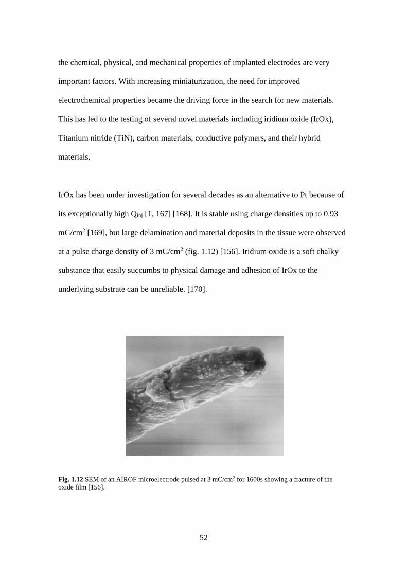
IrOx has been under investigation for several decades as an alternative to Pt because of
its exceptionally high Qinj [1, 167] [168]. It is stable using charge densities up to 0.93
mC/cm2 [169], but large delamination and material deposits in the tissue were observed
at a pulse charge density of 3 mC/cm2 (fig. 1.12) [156]. Iridium oxide is a soft chalky
substance that easily succumbs to physical damage and adhesion of IrOx to the
underlying substrate can be unreliable. [170].
Fig. 1.12 SEM of an AIROF microelectrode pulsed at 3 mC/cm2 for 1600s showing a fracture of the
oxide film [156].

53
TiN is chemically and mechanically stable with high conductivity and Qinj [1]. Typical
values of Qinj are reported around 0.9 mC/cm2 with a hydrolysis limits of -0.9V to 0.9V
for 4000 µm2 electrode at 0.5 ms pulse width [1, 150]. The electrochemical resistance is
lower than Pt due to the very high electrochemical surface area of this material. TiN
delivers charge to neural tissue through a purely capacitive charge injection mechanism
[1, 150]. Electrodes can be fabricated by sputtering TiN onto other materials [171]. It
may be patterned by photolithography and may be a candidate for retinal electrode
arrays and some nerve cuffs designs [1]. Its long-term biocompatibility, however, is
still uncertain [150]. Tantalum/tantalum oxide (Ta/Ta2O5) was thought to be a good
capacitive electrode material and has been extensively explored for nerve stimulation
but it has disadvantages. Such as due to pore resistance its Qinj cannot be increased and
relatively high bias voltages (> 4 V) is required during the interpulse period [1].
Conductive polymers may be suitable alternatives to a metallic electrode for neural
prostheses and have been studied in the last decade initiated since the 1970s [133]
showing evidence of better electrochemical performance in vitro [172] and in vivo
[170]. Among the conductive polymers Poly (3,4-ethylenedioxythiophene) (PEDOT) is
considered as the most promising due to its suitable electrochemical properties and
biocompatibility [173] for neural interfacing. In vitro testing shows that it has a charge
injection limit of 2.3 mC/cm2 and charge storage capacity of 76 mC/cm2 [174-176].
Also, the acute in vivo evaluation reports that PEDOT has increased impedance than
that of in vitro but has higher Qinj than metal electrodes [177, 178]. However, the
structural stability of PEDOT is low as a stimulating electrode and may crack and lose
all of its advantages in vitro or in vivo [174, 176]. Blending with different materials may
improve its mechanical properties but have little possibility of sticking onto substrate

54
materials and may crack too [172, 179-181]. On the other hand, the blending
mechanism of two polymers is not yet understood well, therefore it is not easy to have
the proper ratio of blending materials for desired characteristics of the composite [161].
Carbon nanotubes (CNTs) consist of rolled-up single or multi-walled graphite sheet(s)
[182, 183]. CNTs have the high mechanical strength and excellent thermal conductivity
(3000 W m-1 K-1) [184]. They have a high ratio of electrochemical surface area to the
geometrical surface area, which provides a large double-layer charge capacity [185] and
hence Qinj. The safe charge injection limit of CNT containing coatings have been
reported to be between 1.6 and 2.5mC/cm2 [186, 187]. However, without chemical
modification or embedding in a polymer matrix CNTs do not adhere to substrate
materials.
Diamond has long been recognized as a material with a number of extraordinary
properties [188]. During the 1950s, high-pressure high temperature (HPHT) synthesis of
diamonds meant that the extraordinary properties of diamond were made available in a
number of industries, chiefly in cutting tools where the extreme hardness of diamond is
advantageous [189, 190]. It was not until the 1980s that chemical vapor deposition
(CVD) became a popular method to produce diamond [191-194]. One advantage of this
method over HPHT is that films of diamond could be grown on substrates. Due to the
high hardness and low chemical reactivity, these films are often used as wear resistant
or anti-corrosion coatings [195-198]. Wear-resistant coating for artificial hip joints was
the first medical use of diamond and the first proof of diamond’s high bioactivity [198-
202]. For the various forms of diamond have been developed gradually including
microcrystalline films (1-3µm grain size), nanocrystalline (10-100 nm grain size), ultra-

55
nanocrystalline (3-7 nm grain size) diamond based on gas mixture (recipe) in CVD [92,
203-206].
Doping of diamond, in particular with boron leads to a material with useful levels of
electrical conductivity. [152, 207]. Boron-doped diamond electrodes show an
electrochemical interface with very low double layer capacitance [208, 209] and hence
are not suitable for neural stimulation.
Various groups have developed methods to fabricate macroelectrode and/or
microelectrode arrays of boron doped diamond for recording or electrochemical sensing
applications [210-213]. Bergonzo et al. patterned the diamond seed layer before
diamond growth and thus patterned synthetic diamond films on silicon were directly
obtained from CVD [2, 208, 214]. In practice, most common, multi-electrode arrays
were built by removing material from a continuous conducting diamond films to
produce isolated single electrodes [215-219]. An alternative method was performed by
Ganesan et al. to fabricate a nitrogen-induced ultra-nanocrystalline diamond (N-UNCD)
electrode array of 256 microelectrodes in which electrodes were separated by removing
the film between electrodes by laser milling [220]. In that work, diamond also formed a
hermetic electrical feedthrough in conducting diamond and a method was described to
fill the back of the array with a metallic braze, making the array suitable for direct
bonding to microelectronics (shown in fig. 1.13 A). This group also proposed to
fabricate penetrating diamond electrodes by growing narrow diamond films in an etched
silicone mould (fig. 1.13 B) [221]. Hadjinicolaou et al. first demonstrated neural
stimulation with diamond using single N-UNCD electrodes (200 × 200 µm) brazed onto

56
a 100 mm thick tantalum foil shank (fig. 1.14 a). An extended view of an electrode of
diameter 600 µm (fig. 1.14 b) was used to assess electrochemical stability [222].
Fig. 1.13 A) A flat N-UNCD high-density microelectrode array isolated by laser milling (left). B)
Templated diamond spikes produced by Ganesan et al. (Right) [220, 221].
Fig. 1.14 (a) SEM image of a 200 × 200 mm square N-UNCD electrode that has been used as a
stimulating electrode on excised rat retina. Inset is a micrograph of the electrode before insulation with
epoxy and silicone. (b) An SEM image of a 600 mm diameter N-UNCD disc electrode used to assess
electrochemical stability. Inset is a micrograph of four such electrodes attached to a flexible circuit board
and isolated with epoxy resin [222].
1.3 Biomolecular coating on the electrode surface
1.3.1 Electrode tissue interaction
The physical properties of an electrode surface play a vital role in its efficacy. Along
with the interfacial energy, wettability, charge distribution and available contact area on
the surface for neurons are correlated to the surface roughness which directly influences

57
protein adsorption as well as cell attachments on the surface [223]. Thus, an optimum
surface roughness is important for a cell attachment and subsequent axonal proliferation
[224, 225]. Proteins and other organic compounds may adsorb to the electrode surface
in vivo depending on the electrode surface chemistry. Adverse tissue reactions reduce
charge transfer from the electrode to the tissue and increase the electrochemical
impedance of electrodes [168] which impedes efficient chronic stimulation. Chronic
electrical overstimulation can also cause tissue damage [226]. Addressing these
problems chronic stimulation of nervous system using neural prostheses is a pressing
issue. However, intimate interfacial contact of electrodes to tissue is expected to
improve the efficacy of electrodes and help to achieve selective stimulation and
recording chronically with higher resolution. Therefore, preserving structural,
mechanical and electrochemical properties and non-toxicity of electrode materials by
electrode surface coating of organic molecules may be promising to improve the
biocompatibility and consequently the neural interaction at the electrode-tissue
interface.
1.3.2 Biomolecules for coating
The degree of freedom for biomolecular coatings is wide. Anti-inflammation agents and
neurotrophins and adhesion molecules are widely used on electrode materials to
improve their biological interactions. In vitro and in vivo investigations on electrode
coatings to enhance biocompatibility through cell growth, proliferation, differentiation,
neurite growth rate and histopathological studies have yielded promising results. A
range of biomolecules investigated for coating are presented in table 1.4 [160].

58
Table 1.4 Combinations of coatings and biomolecules to investigate the improvement
of electrode-neuron interfacing [160]
HA, hyaluronic acid; αMSH, α-melanocyte stimulating hormone; NGF, nerve growth factor; PDGF-BB, platelet
derived growth factor-BB; IGF-1, insulin-like growth factor- 1; BDNF, brain derived neurotrophic factor; GDNF,
glial cell-derived neurotrophic factor; NT-3–neurotrophin3; PEG, poly (ethylene glycol); PEG-PLA, poly (ethylene
glycol)-poly (lactic acid); and CNT, carbon nanotube
Application Coatings on electrode
surface
Biomolecules attached on
coatings
Reference
Cell attachment PEDOT DCDPGYIGSR and
DEDEDYFQRYLI
[227]
PEDOT Fibronectin fragments
DCDPGYIGSR
[228]
PPY Fibronectin fragments
Nonapeptide
CDPGYIGSR
[229]
Carbon nanotube (CNT) Collagen type IV [230]
Anti-
inflammatory
PPY HA [231]
PPY Dexamethasone [232]
PEDOT electrodeposited
on PLGA nanofibers
Dexamethasone [233]
Polyterthiophene Dexamethasone phosphate [234]
Nitrocellulose αMSH [235,
236]
Silicon αMSH [88]
Multiwalled CNTs Dexamethasone [187]
Growth factor (to
improve cell
adhesion)
Methylcellulose
PDGF-BB and IGF-1 [237]
Poly (ethylene-co-vinyl
acetate) (EVA) (EVA
rods)
NGF, NT-3, BDNF and GDNF [238-240]
Agarose NGF and Laminin [241]
Collagen NT-3 [242]
PPY Laminin fragments
RNIAEIIKDI (p20)
[243]
Multiwalled CNT NGF [244]

59
These approaches have limitations as anti-inflammatory molecules deplete from the
coating on the electrodes and thus it is hard to maintain desired lower inflammation at
the interface. Utilization of neurotrophins, such as brain-derived neurotrophic factor
(BDNF) [245] and nerve growth factor [245] within electrode coatings, promotes an
initial burst of neuronal process growth towards the electrode interface. Some groups
have shown that neurite growth rate reduces after the depletion of nerve growth factor
[245, 246]. Blending of biomolecules with conducting polymer, CNT and/or hydrogel
for coating onto electrode interface is also suffering from different limitations
diminishing the desired electrical and mechanical properties of the composites [227,
228, 231, 247].
Fig. 1.15 Schematic diagram of the extracellular matrix (source: Rose L. Hamm, McGraw-Hill
Education).

60
Fig. 1.16 Schematic diagram of laminin molecule structure and function (source: Pearson education. Inc.
publishing as Benjamin Cummings, 2003).
Extracellular matrix components (fig. 1.15) that promote cellular attachment, cell
growth, homeostasis, differentiation, and cellular motility. Each of the molecules and
their relevant peptide sequences have a role in mechanical, biological and chemical
stimulation to enhance neural growth and development [53, 248-250]. Collagen
provides structural strength but also resists pulling forces against the cell. Fibronectin
promotes cellular movement and branching through cell binding on the interacting
substrates in the direction of its pathway.
Laminin is a heterotrimer assembled from α, β, and γ chain subunits (fig. 1.16), secreted
and incorporated into cell-associated extracellular matrices. Laminins self-assemble,
bind to other matrix macromolecules, and have unique and shared cell interactions
mediated by integrins, dystroglycan, and other receptors. Through these interactions,

61
laminin contributes to cell growth and differentiation, cell shape and movement,
maintenance of tissue phenotypes, and promotion of tissue survival and protection.
Chan et al. proposed that extracellular matrix molecules could provide structural and
chemical cues to regenerate neural functions at neural interfaces [217].
Laminin has multiple cell binding sites [224] (fig. 1.16) and initiates receptor-mediated
cell binding with focal adhesions for intra and extra cellular signal transfer [251].
Laminin and laminin peptides can be incorporated in CNT, conductive polymer (CP) or
conductive hydrogel (CH) coatings or in their composites by simple adsorption,
entrapment or covalent binding. Adsorption does not produce a stable interface under in
vivo conditions as the surrounding proteins can displace the adsorbed molecules due to
competitive binding processes. Entrapped molecules, however, can diffuse away
through coatings or become obstructed within the coating due to coating porosity and
thus the molecules may not be accessible for cell growth or attachments. Covalent
bonding of these molecules or their components is preferable to coat onto an electrode
surface, as it is relatively stable [160, 251]. Therefore, in the present work, laminin is
coupled to diamond films/electrodes covalently.
1.4 Diamond is the material of choice in this study
The miniaturization of implants will reduce space constraints to implant the devices into
the body of patients, expecting more safety and comfort. The background of three major
research problems which impede the developments of miniaturized medical implants
has been discussed earlier sections in this chapter. Diamond has several extraordinary
properties and at present different forms (conductive and non-conductive) of diamond

62
can be synthesized and/or coated on substrates in CDV reactor system (section 1.2.4).
Therefore, this technology along with other advanced fabrication facilities could be used
to develop hermetically sealed microcoils embedded in diamond. This attempt could
create the opportunity to use higher conductive materials for coil wire even though they
are not biocompatible. This technology can also be used to coat Pt electrode surface
with conductive diamonds expecting to increase their Qinj. In addition, biomolecules
like laminin (protein) attachment on the diamond coating could improve the electrode-
tissue interactions.
The utilization of diamond in biomedical implants is still very limited, which reflects
that intensive investigations are required for the usage of the diamond along with the
transitional platinum-technology for biomedical implants. Therefore, in the present
work diamond was the choice of material to investigate the followings:
a) Fabrication of miniaturized coils hermetically embedded in diamond for continuous
wireless power transfer to the implants efficiently and the use of silver active braze
alloy (Ag ABA) as a wire material.
b) Fabrication of electrodes from diamond films deposited on roughened platinum and
oxygen plasma activated diamond films to evaluate and compare them with traditional
platinum electrodes.
c) Biomolecular (laminin, a protein from the extracellular matrix) coating on to the
deposited diamond films as well activated diamond films to observe its impact on the
electrochemical properties of diamond electrodes and the cell adhesion on the films.

63
CHAPTER 2
Wireless Induction Coils Embedded in Diamond for Power
Transfer in Medical Implants
ABSTRACT
Wireless power and data transfer to medical implants is a research area where
improvements in current state-of-the-art technologies are needed. This is primarily
driven by the strong desire to miniaturize implants. At present, lithographic patterning
of evaporated metals is widely used for miniature coil fabrication. This method
produces coils that are limited to low micron or nanometer thicknesses leading to high
impedance and thus limited power transfer efficiency. In the present work, we describe
a novel technique, whereby trenches were milled into a diamond substrate and filled
with silver active braze alloy, enabling the manufacture of small, high cross-section,
low impedance microcoils capable of transferring up to 10 mW of power up to a
distance of 6 mm. However, a continuous metal loop simulating a metallic braze line
used for hermetic sealing, when placed parallel and close to the coil surface, reduced
power transfer efficiency by 43%. The effect was not significantly high when the loop
was placed perpendicular to the microcoil surface. Encapsulation of the coil by the
growth of a further layer of diamond was achieved with minimal impact on power
transfer efficiency. Accelerated ageing tests after encapsulation showed that these coils
are long-lasting. Our results demonstrate the feasibility of fabricating a high-cross
64
section, biocompatible and long lasting miniaturized microcoil that could be used in
either a neural recording or neuro-stimulation devices.
Biomed Microdevices (2017) 19: 79
DOI 10.1007/s10544-017-0220-1
Published online: 26 August 2017
© Springer Science+Business Media, LLC 2017

65
2.1 Introduction
Medical bionics is the branch of medical science and technology that deals with
intractable and incurable medical conditions to reduce their severity or provide
therapeutic treatment using prosthetic and neuromodulation devices. The field has
significant market potential owing to a wide range of diseases that the technology can
target [7, 8, 252]. A number of medical implants are very commonly used, such as
cochlear implants, intravascular stents, deep brain stimulators, and visual prostheses.
One notable trend is the increase in the emergence of artificial neural implants that
either record from, or electrically stimulate, peripheral or central neurons.
In order to perform this function, implants require a continuous, efficient power supply
[253] that would preferably transmit power wirelessly, thus minimizing the risk of
infection, patient discomfort, pain, health care costs and the need for implantable
batteries. Inductive power transfer is, therefore, a necessary technology in developing
safer, more robust devices with a lower risk of tissue damage caused by long periods of
continuous transcutaneous connections [67, 253-255].
The efficiency of wireless power-transfer strongly depends on a variety of parameters
such as the materials used, coupling and distance between the transfer and receiver coils
and their geometrical dimensions, for example, the length and cross-section of the coil
wire. Besides the outer and inner diameter of the coils, properties of the encapsulation
materials influence the overall efficiency of the implant system [58, 253]. The
efficiency of coils is measured by their quality factor (Q-factor), which is defined as the
ratio of the electromagnetic energy transmitted (Etr) to the receiver coil and energy
dissipated (Edis) through it according to Equation (2.1).

66
𝑄 =𝐸𝑡𝑟
𝐸𝑑𝑖𝑠= 𝜔°
𝐿
𝑅𝑠 … … … … … … … … … … … … … … … … … … … … … (2.1)
Where 𝜔° is the operating frequency, L is inductance and Rs is series resistance
In cochlear and retinal implants, while inductive power transfer systems are being used,
the receiver coils are large in dimension (in the centimeter range) and implanted
subcutaneously behind the ear anchored to the skull [2, 253, 254]. In recent decades, the
development of microelectronics has provided opportunities for the miniaturization of
neural implants. Recently, very small devices designed to be implanted within small
body structures such as the eye [152, 220, 222, 256, 257], or inside cortical blood
vessels [258] have been developed. The recent surge in interest in electroceuticals for
treatment of a range of disorders has led to a myriad of neuromodulation targets, such as
the vagus nerve, for regulation of tumor necrosis factor (TNF) associated with
autoimmune diseases of the digestive system (Crohn’s disease) and rheumatoid arthritis
[259, 260]. Many of these diseases are chronic and neuromodulation devices to treat
them or restore sensation would ideally be implanted for long time periods. Such
devices have the potential to offer significant quality of life improvements but there are
a major power delivery challenges when devices are small and implanted distant from
the skin surface. For these devices, it is necessary to develop a miniaturized receiver
microcoil.
Most commonly, microcoils are fabricated by photolithographic methods. For very fine
structures, methods such as X-ray lithography, electron-beam lithography, and ion-
beam lithography can be employed. Features in the range of 10 nm can be achieved
[261]. Microcoils fabricated using these methods, however, are extremely thin in cross-

67
section resulting in high electrical resistance and the inability to deliver sufficient power
inductively to the implant. Li et al. designed and fabricated a two layered (each layer
consisted of 10 turns) gold coil of 3 µm thickness with an outer diameter of 9 mm and
an inner diameter of 5mm on a Parylene C coated silicon substrate via
photolithography. The maximum power of about 43 mW could be delivered at a
distance of 1 mm using an inductive link but the power was reduced by 62% at 2 mm
distance due to divergence of the electromagnetic field and the delivered power
reduced to 10 mW, where the maximum detectable range was only about 4 mm [2].
In addition to the coil design and fabrication, the material used for coil wire is also very
important. The coil wire material should have high conductivity for efficient power
transmission [67, 253, 262]. Various materials are being used to make coils such as gold
[2, 263], gallium or gallium alloys [263] and aluminum [253, 264]. In this study, we
considered the use of silver-based active brazing alloy (ABA) for coil fabrication. Silver
ABA is currently being used for interconnections in the electronic packaging industry
for their solderability [265] and can also serve as a metal film conductor having a low
electrical resistivity of 2.2 × 10⁻⁸ ohm.m, only 38% higher than that of pure silver (1.59
× 10-8 ohm.m). Silver ABA also produces low porosity films and has excellent film-
substrate adhesion to diamond [265]. These properties make silver ABA an attractive
choice of material to fabricate a coil. However, whilst the material has some excellent
properties it is unsuitable for use in medical implants without encapsulation as it
exhibits very poor biocompatibility [256].
Effective power transfer not only requires an efficient inductive link but also requires
that losses due to parasitic inductive currents induced in the encapsulation, for instance,

68
be minimized. Interactions of the hermetic encapsulation of the implants with the
inductive coils, therefore, is a design consideration for maximizing clinical effectiveness
and safety over the long-term [90-92]. Various materials have been investigated for
encapsulation of medical implants such as parylene C [2, 253, 266], polyimide [2] [11],
rigid titanium boxes, silicone [267], gold ABA [256] and diamond [256]. Generally,
metals are preferable for hermetic sealing of electronic packages, as polymers can
degrade and become porous while brittle materials such as glasses are at risk of
breakage. Metals, however, are electrically conductive effectively forming a ‘short-
circuited turn' adjacent to the coils when inductive power is transferred to the implants.
This, in turn, can affect the efficiency of the inductive power link due to eddy currents
in the magnetic field [268]. Thus, it is preferred to encapsulate the coil and electronics
package using a non-conductive material. Even if a non-conductive material can be used
for encapsulation, however, hermetic sealing may still require a metallic braze line to be
incorporated in the device. For example, Lichter et al. employ a gold ABA braze line as
a method of sealing two halves of a diamond hermetic capsule together [256] in a
similar fashion as shown in fig. 2.1
In order to respond to the above limitations, we have developed a new fabrication
method of planar square spiral microcoils made using silver ABA completely embedded
within the non-conductive diamond. The coils have a large rectangular cross-section
thus reducing resistance and increasing Q-factor. The microcoils in this work are
capable of providing about 10 mW of transferred power across 0.51 kΩ at a distance of
6 mm which should be sufficient to power an implanted device for neural stimulation
and/or recording. As the toxicity of silver ABA is an issue, we also describe a method to
encapsulate the microcoil with an additional layer of diamond and test its effects on
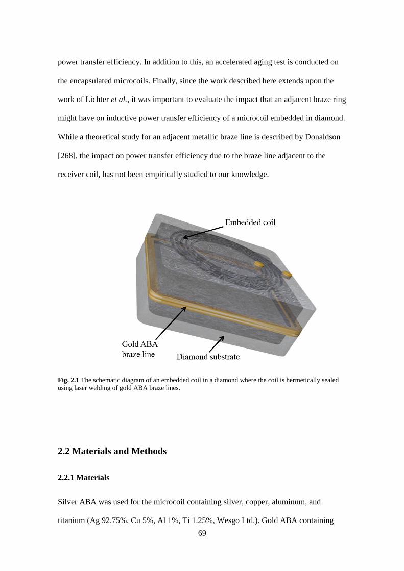
69
power transfer efficiency. In addition to this, an accelerated aging test is conducted on
the encapsulated microcoils. Finally, since the work described here extends upon the
work of Lichter et al., it was important to evaluate the impact that an adjacent braze ring
might have on inductive power transfer efficiency of a microcoil embedded in diamond.
While a theoretical study for an adjacent metallic braze line is described by Donaldson
[268], the impact on power transfer efficiency due to the braze line adjacent to the
receiver coil, has not been empirically studied to our knowledge.
Fig. 2.1 The schematic diagram of an embedded coil in a diamond where the coil is hermetically sealed
using laser welding of gold ABA braze lines.
2.2 Materials and Methods
2.2.1 Materials
Silver ABA was used for the microcoil containing silver, copper, aluminum, and
titanium (Ag 92.75%, Cu 5%, Al 1%, Ti 1.25%, Wesgo Ltd.). Gold ABA containing

70
gold, nickel, and titanium (Au 96.4%, Ni 3%, Ti 0.3%, Wesgo Ltd.) was utilized as the
braze line material. Microcoils were embedded in polycrystalline diamond (PCD)
substrates (Element 6 T100 grade). A mixture of sulfuric acid (95-97% reagent grade,
ISO) and sodium nitrate mixture was used to clean PCD substrates. Probe connection
wires were made of platinum (A-M systems, Pt-Ir, 0.005ʺ bare) and/or copper (Cu) and
attached to the coils for measurement purposes. PCD was grown on the exposed surface
of microcoils from a mixture of methane and hydrogen gas (BOC Australia) for full
encapsulation. Araldite epoxy was used to cover the connection wires during the ageing
test.
2.2.2 Design and fabrication method of microcoils embedded in diamond
A flow chart of the design and fabrication process of microcoils is shown in fig. 2.2 (a).
Planar square spiral coil trenches with different width, depth, and separation between
two adjacent turns were laser milled into PCD substrates to compare different coil
versions. At the two ends of the spiral trench, holes were laser milled right through the
PCD substrate for each sample such that the microcoils ended up as pads on the under-
side of the substrate during silver brazing for connection of wires. The laser milled PCD
substrates were acid boiled in a mixture of 97% sulfuric acid (5 ml) and sodium nitrate
(25-50 mg) for one hour. After acid boiling substrates were cleaned sequentially in
acetone and distilled water. The width and height of the microcoil trench and the
separation between two consecutive coil turns were measured by scanning electron
microscopy (SEM; FEI Quanta, FEG 200, fig. 2.2(b)) and optical profilometry (fig.
2.2(c)). Silver ABA paste was poured into the coil trench and melted using an MTI
vacuum furnace. The furnace was evacuated to a pressure of 5 - 6×10⁻⁶ Torr and the

71
temperature ramped up to 960 ºC. The samples were held at 960 οC for 10 min and then
the temperature was ramped down to room temperature gradually. Excess silver ABA
was polished out mechanically using a Coborn PL3 planetary lapping machine. SEM
images were taken post cleaning. Finally, connection wires were laser welded onto the
pads on the under-side of the microcoils (fig. 2.2(d)).
Fig. 2.2 (a) Sequence of microcoil fabrication process, (b) SEM of microcoil trench, (c) Optical
profilometer image of microcoil trenches (bottom of the trench is in blue) and (d) SEM image of a 4.6 ×
4.6 mm coil with 20 turns of silver ABA after fabrication
2.2.3 Electrical characterization method
The electrical characterization of microcoils is the measure of its Q-factor, DC resistance,
and inductance. A frequency response analyzer (AP Instruments Inc., Model 300) was

72
used for microcoil characterization. This analyzer had a frequency range from 0.10 Hz to
30 MHz. The above electrical parameters were measured with respect to frequency.
2.2.4 Wireless power transfer and braze line effect measurement method
Power transfer and power receiver units were constructed according to the schematic
diagram shown in fig. 2.3. A power transfer unit was connected to a DC power supply
(model TPS-4000). A 3 cm circular transmitter coil (Nucleus patient coil Z209880
manufactured by Cochlear Ltd, fig. 2.3) was attached to the power transfer unit. This
unit consists of a tuned circuit and integrated RF coil driver. The DC input supply
voltage of the power transfer unit was 3.3 volts and the input current was approximately
135 mA (135 mV measured across 1 Ω). Radio frequency (RF) waves of 4.82 MHz
were generated and tuned near to self-resonance of the receiver microcoils by a RF
generator (HP Hewlett Packard, 33120A). In order to measure inductive power transfer,
the microcoils were placed 6 mm away along the axis passing through the center of the
transformer coil. The eight best fabricated microcoils were tested separately using the
same receiver unit. A rectifier circuit was used to obtain output power across various
loads. Input current and the output voltage at different load resistances (R, fig. 2.3 (a))
were measured with a multimeter (RPG, DM8100). To assess effects of brazing on
efficiency, a gold braze line (5.1 × 5.1 mm) fabricated on a separate diamond substrate
was introduced either directly on the surface of the microcoil in a parallel orientation
(fig. 2.3 (b)) or in a perpendicular position 0.2 mm away from the outer diameter of the
microcoils (fig. 2.3 (c)) whilst connected to the measurement circuit.

73
Fig. 2.3 Schematic diagrams: (a) circuit of the transceiver unit, (b) parallel position of gold braze line to
the plane of microcoil and (c) perpendicular position of gold braze line to the plane of the microcoil.
2.2.5 Coil encapsulation method
Following initial baseline measurements, an additional layer of PCD was deposited onto
the exposed surface of the microcoils in an Iplas microwave plasma-assisted CVD
system. Microcoils were seeded before PCD deposition with nanodiamond (Nano
Armor) by ultra-sonication in ~3-5 nm nanodiamond/methanol solution for 5 minutes.
Compressed air was used to dry the samples. A gas mixture of 500 sccm hydrogen and
10 sccm methane (BOC Australia, purity 99.99%) was used. During the growth period,
the microwave power was maintained at 900 W, gas pressure at 60 Torr and stage
temperature at 800 ºC. The PCD layer was grown for several hours and Elemental
analysis (EDS) of the PCD film was performed to diagnose the exposure of silver
through the PCD layer.

74
2.2.6 Accelerated ageing method
Samples were placed in a capped, small, clean glass bottle fulfilled with 0.9% medical
grade sterile saline (Aerowash Sterile Sodium Chloride Eyewash Solution). The bottles
were transferred to an environmental chamber (Micro Climate Benchtop Test Chamber
Cincinnati Sub-Zero) kept at 85º C. Images were recorded using SEM before and after
ageing for time periods of 30 days corresponding to approximately 30 months of real-
time equivalent at 37 oC in a saline environment. An aging factor (Q10) of 2 was used for
all accelerated aging calculations.
2.3 Results and Discussions
2.3.1 Microcoil fabrication outcomes
Eighteen 4.6 × 4.6 mm microcoils were fabricated using four sets of parameters
according to the values presented in table 2.1. Table 2.1 also provides the measured
resistance and Q-factor for each of the four sets of microcoils. In order to observe the
effect of depth and width of microcoils the depth (h = 100 µm) of set 2 and width (w =
80 µm) of set 3 were different from that of the set 1 while the outer dimension (4.6 mm)
and number of turns (N = 4) were same. In case of set 4, the number turns (N = 20) was
more than set 1 (N = 4) including much wider cross-sectional area of turns. The results
show that the Q-factor is dependent on width, depth and number of turns. The actual
values of width, depth, and separation between two consecutive turns presented in the
table were obtained from optical profilometry images which were in most cases close to
the expected values in parentheses. Generally, the separation between two consecutive
turns was found to be lower than expected while the width of trench was found to be
several micrometers over that of the expected values during laser milling, most likely

75
due to the conical shape of the laser used for milling. The depth of the coil trench,
which also varied by several micrometers in some places, was over that of the targeted
depth during laser milling. There was difficulty in obtaining imaging data from the
bottom of the trench for microcoil set 2 due to the small width, so depth values for this
set were significantly underestimated. As the eight microcoils from set 4 were superior
to samples from the other sets in terms of lower DC resistance and higher Q-factor, in-
depth further experiments were conducted only on this microcoil set.
Table 2.1 Resistance and Q-factor (average ± std. error) of four sets of coils embedded
in diamond with several design parameters. Values in parentheses show
targeted/expected parameters. *Difficulty in getting accurate depth data from this set of
coils
Sets and
number
of coils
Outer
diameter
in mm
Width (w)
µm
Depth (h)
µm
Separation
Between
turns in
µm
Numbe
r of
turns
Average
resistance
(RDC) Ω
Maximum
Q-factor
Set 1
(n=4)
4.6 31.20±1.67
(21)
35.34 ±0.78
(35)
62.05±1.84
(70)
4 5.18±0.5
8
1.21±0.08
at ~11MHz
Set 2
(n=4)
4.6 34.30±1.85
(21)
39.12±2.53*
(100)
59.80±1.53
(70)
4 2.38±0.1
1
1.98±0.05
at ~8 MHz
Set 3
(n=2)
4.6 84.39±1.15
(80)
35.07±0.17
(35)
70.80±0.85
(70)
4 1.35±0.0
5
2.69±0.08
at 5.88 MHz
Set 4
(n=8)
4.6 46.3±0.41
(50)
120.45±1.15
(140)
54.00±0.33
(50)
20 2.25±0.0
5
3.87±0.23
at ~3.2 MHz
Fig. 2.4 (a) shows an SEM image of one of the microcoils from set 4. The bottom of the
coil trench was found to be narrower than that of the top due to the focusing angle of the
cutting laser. A sidewall angle was typical ≤ 11 degrees in all our samples. SEM images
after polishing and cleaning showed instances of small cracks in the PCD between coil

76
turns as shown in fig. 2.4 (b). In our study, the cracks did not short two consecutive
turns. However, there is an inherent risk of shorting between turns negatively impacting
Q-factor if these cracks would fill with braze. These cracks might be reduced by
controlling brazing temperature profiles so that PCD substrates do not bend during
heating and by using smooth wheel surfaces during mechanical polishing. Also, lower
speed polishing may reduce the appearance of cracks.
Fig. 2.4 (a) Top view SEM image of a microcoil from set 4, (b) SEM image of a crack in PCD between
two turns.
Fig. 2.5 (a) Average resistance (n = 8, average ± std. error) and (b) Average Q-factor of the eight
microcoils (n = 8, average ± std. error) from set 4. X-axes are in log scale.

77
2.3.2 Electrical characterization
The Q-factors and AC resistance of the microcoils from set-4 are graphically depicted in
fig. 2.5 with respect to frequency. The measured resistance of the microcoils gradually
increased as a function of frequency (fig. 2.5 (a)). The maximum value of Q-factor of
the microcoils was 4.05 at 3.89 MHz (fig. 2.5 (b)). The small variation (± 0.052) in Q-
factor and resistance (± 0.33 Ω) provided evidence of the reproducibility in
manufacturing as the temperature during brazing was better controlled than that of the
other microcoil sets 1-3.
2.3.3 Wireless power transfer and braze line effects
Fig. 2.6 (a) shows the amount of average power transfer across different load resistances
from 0.51 -7.51 kΩ. The measured maximum output voltage was of 2.41 volts and an
average power of 8.64±1.62 mW (n=6 coils) was obtained across a 0.51 kΩ load with
the highest transmitted power up to 11.38 mW. The power transfer efficiency of the
microcoils as a percentage across different load resistances is shown in fig. 2.6 (b). The
average power transfer efficiency was 1.96 ± 0.35 % across a 0.51 kΩ load without the
presence of any braze line. When comparing our transmitted power results to coils
manufactured using lithographic techniques, we were able to transmit almost the same
power with a coil of nearly half the dimensions. Also, the coils made using lithographic
techniques were not able to send power beyond 4 mm [2] but our microcoils are capable
to transfer power up to 6 mm away along the axis of the transmitter coil. Transmitted
power of 10 mW would be sufficient for neural recording by a chip of 32 channels
which consumes a total power of 5.4 mW [269]. This power could also be sufficient for

78
a neuromuscular or optogenetic stimulation device [270, 271].
Fig. 2.6 (a) Transmitted average power and (b) average power efficiency, plotted against load resistance
for the 4.6 mm diameter coils (n=6) described in table 2.1 from set 4 at a distance of 6 mm between the
transmitter and receiver coil, (c) Shows the impact of a parallel gold braze line (5.1 × 5.1 mm) on power
transfer efficiency of the three highest Q-factor microcoils taken from set 4, The plots show the change in
power efficiency (across 0.51 kΩ) of the microcoils with increasing distance of the braze line, (d) Shows
a comparison of power transfer efficiency for the same three coils as (c) between a braze ring parallel to
the coil and a braze line placed 0.2 mm away from the outer edge in a perpendicular orientation with
respect to without any braze line.
Fig. 2.6 (c) indicates the impact of a braze line on the power efficiency for three of the
eight microcoils of higher Q - factors with increasing distance between the braze line
and microcoils. It was observed that the effect of a gold braze line oriented parallel to
the microcoil did not affect power efficiency when placed more than 2 mm away from
the plane of the microcoil (fig. 2.6 (c)) but could reduce power efficiency by up to 43%
when placed directly on the coil (0 mm). However, when the braze line was placed
perpendicularly to the plane of the coil 0.2 mm away from the outer edge, the power
transfer efficiency was not affected significantly compared to the power efficiency of
the coils without any braze line.

79
2.3.4 Effects of encapsulation and accelerated ageing
Encapsulation of microcoils was performed in two stages. Firstly, a group of 4 out of 8
microcoils from set 4 were encapsulated by a PCD layer grown for 5 h applying the
methodology described earlier (section 2.2.5). Secondly, a separate group of 2
microcoils were encapsulated by the PCD layer grown for 14 h with the same
conditions as applied to the first group. A typical mapping at four different spots of a
Raman spectrum was observed as in fig. 2.7 where peaks were at around 1332 cm-1 as
an indication for PCD [272]. The remaining 2 microcoils were subjected to an ageing
Fig. 2.7 Raman spectra (λ = 532 nm) obtained from the PCD layer on Ag ABA trenches (spots 1-2) and
on diamond islands separating two consecutive turns of the coil (spots 3-4).
test without encapsulation. Microcoils were grouped in a random manner. Fig. 2.8 (a)
and (b) show SEM images at two different magnifications for one of the encapsulated
microcoils. As seen in the images, larger diamond crystals were found to grow on the
space between coil turns while finer crystals grew over the trench. Elemental analysis
(EDS) of the PCD film, revealed no silver peaks for only one of the microcoils
encapsulated by PCD using a 5 h (fig. 2.9) growth time. In contrast, both microcoils in
the second group encapsulated by PCD using a 14 h growth time were free of silver
peaks (fig. 2.9). After electrical measurements on encapsulated microcoils, an ageing

80
test with the conditions described in methodology was conducted on all samples
exhibiting full encapsulation (1 coil from the 5-hour group and both coils from the 14-
hour group).
Fig. 2.8 (a) SEM image (top view) of a microcoil after PCD growth on the exposed surface, (b)
Magnified (1000x) SEM image of the red box in the fig. (a). Figures c-f show the change in Q-factor for
samples before and after PCD growth, after accelerated aging and after oxygen plasma treatment
respectively. The PCD growth times for the samples were (c) 5 h, (d) & (e) 14 h and (f) shows the data
corresponding to one of the two samples where the silver coil was aged without PCD growth.

81
The ageing test was conducted for 30 days at 85 ºC as described in the methods over 3
encapsulated and 2 non-encapsulated microcoils. Plots depicting the change in Q-factors
before and after PCD growth, after an aging test and eventually after oxygen plasma
treatment of the samples are shown in fig. 2.8 (c), (d), (e) and (f) respectively. When
performing measurements after encapsulation, it was observed that the equivalent AC
resistance of the microcoils increased and consequently the Q-factor decreased by 38%
over the 3 encapsulated samples (fig. 2.8 (c), (d) and (e)). The Q - factor of the 5-hour
encapsulated microcoil (fig. 2.8 (c)) was found to be higher than that of the two coils in
the 14-hour group (fig. 2.8 (d) and fig. 2.8 (e)), indicating that a thinner PCD layer may
have less impact on the reduction of Q - factor albeit with the high risk of exposure of
silver ABA. It is worth mentioning that the Q - factor improved to some extent after
accelerated ageing of the encapsulated samples. Subsequent resistivity measurements
over the grown PCD films showed that the PCD layers on the coils surface were
conductive due the possible presence of graphitic material which may have caused the
drop of the Q-factor. It is important that the DC resistance of the microcoils remained
the same, which indicates that the microcoils embedded in diamond were not changed.
On the other hand, a nonconductive oxide layer may have been formed during the
ageing period on the PCD, reducing the conductivity of the films to some extent which
improved the Q. To test this theory an additional oxygen plasma treatment was
conducted on the PCD layer. After oxygen plasma treatment the Q - factor of PCD
encapsulated coils further increased as in fig. 2.8 (c, d, and e) and PCD film surface
became nonconductive. Hence, we conclude that the drop-in performance was due to
unexpected conductivity in the PCD film providing a high resistance short circuit
between coil turns. For future work, it will be important to address a fine balance
between the risk of silver exposure and the nonconductive PCD formation by careful

82
periodic control of the encapsulation growth time and then oxygen plasma treatment for
each layer corresponding to each periodic growth time of PCD on coil surface.
Fig. 2.9 Typical spots for elemental analysis on PCD layer grown on Ag ABA microcoils after ageing
test. A1-A2) Silver peaks of EDS spectrum (A1) performed on the PCD layer of growth time of 5 h (A2).
A3-4) Only the carbon peak was observed in the EDS spectrum (A3) on the PCD layer grown for 14 h
(A4).
Somewhat surprisingly, there was no significant change in Q - factor before and after
accelerated ageing of the microcoils without encapsulation (fig. 2.8 (f)). The most likely
explanation for this is that since silver ABA is an alloy containing silver, copper,
aluminum, and titanium, it may take more time to degrade compared to when using pure
silver. SEM images were taken after the ageing tests but no visible changes in the
diamond encapsulated samples were observed in case of 14 h growth. There was a tiny
spot observed on PCD layer of 5 h growth film that appeared to be damaged. EDS test
was conducted on the PCD films over the samples. EDS test on PCD films grown for 5

83
h over microcoils after accelerated ageing did indicate silver at the surface, leading to
the conclusion that 5 h growth time was insufficient to fully encapsulate the coils. PCD
layers grown for 14 h did not exhibit silver peaks during EDS analysis after accelerated
ageing. A film thickness of 2-3µm is typical after 14 h of growth under the reaction
conditions used. Full encapsulation of microcoils in diamond is therefore possible
provided the diamond film is grown to a sufficient thickness. Measurement of power
transfer efficiency of fully encapsulated microcoils after ageing tests indicated that up to
2.64 mW power can be transferred over 6 mm of air. While 10mW is ideal, 2.64 mW is
still sufficient to power a typical neural recording device or a low power stimulator
[273].
Care should be taken to pour the silver ABA into the coil trench to make sure that there
is no air gap which may introduce defects within the silver ABA wire in the trench.
Optimum temperature control over time is very important to avoid bending of the
diamond substrate which may cause fractures during polishing. The optimum speed and
surface roughness of the polishing wheel and the proper arrangement of planar
placement of the microcoils on the wheel reduces fractures and any other damage of the
microcoils. For hermetic sealing the PCD growth over microcoils in CVD at well below
the melting temperature of silver ABA is very beneficial. As the dimensions of the
microcoil are very small, the major limitation to the power transfer efficiency comes
from the loss of magnetic energy due to spread of the magnetic field with respect to
distance. Therefore, the receiver coils should be as large as practical for the application.
For instance, larger coils can be used under the skin of thickness 2–8 mm [274-276]
depending on body parts and health for wireless sensor networking [277] and
miniaturized drug delivery systems [278] to control externally. In these cases, a

84
significant challenge could come from the lack of RF tuning between transceiver coils
to maximize the power transfer efficiency. Coupling of the coils is also extremely
important. When the microcoil is out of the central axis of the transmitter coil, power
transfer drops.
2.4 Conclusions
We described fabrication, electrical characterization, hermetic encapsulation and
longevity evaluation of microcoils embedded in diamond for wireless power transfer to
medical implants. The results revealed that fabrication of 4.6 mm diameter microcoils,
embedded in diamond, was achievable and reproducible. The microcoils were able to
transfer, 10 mW across 0.51 kΩ at a distance of 6 mm yielding a power transfer
efficiency of approximately 2%. This is sufficient for low powered neural recording and
neuromuscular stimulation. We demonstrated that a continuous short circuit, similar in
diameter and close to the microcoil reduced transfer efficiency significantly. This
impacts on devices that are sealed using a continuous conducting braze line to close the
packaging. Microcoils, completely encapsulated in diamond were fabricated by growing
a further layer of diamond over the embedded coils. The growth of the diamond layer
over the coils reduced the coil Q-factor by an average of 38%. Nonconductive PCD may
be grown using oxygen plasma treatment on PCD layers of several nanometers and
continuing the PCD growth up to enough thickness (likely 2-3 µm) to encapsulate
microcoils which may not change Q - factor. Encapsulated microcoils did not degrade
further during 30 days of accelerated aging at 85 oC in saline (30 months, real-time
equivalent at 37 oC) indicating that the diamond encapsulation would be leak free over,
at least, 30 months in vivo. With the drop in Q-factor, fully encapsulated microcoils

85
were capable of receiving 2.64 mW of power over a distance of 6 mm yielding a
maximum transfer efficiency of 0.65%. The outer diameter of all microcoils was only
4.6 mm and therefore the technology is an attractive option for miniaturization of
wireless power delivery to future implants. As diamond is a hard, hermetic,
biopermanent and biocompatible material, these microcoils are promising for long-term
medical implants.

86
CHAPTER 3
Diamond Coating Improves the Electrochemical
Characteristics of Platinum Electrodes
ABSTRACT
The aim of this study was to fabricate and characterize thin film conducting diamond
electrodes on platinum foil. Many manufacturing techniques have been developed
enabling the use of platinum in medical devices, but very few for diamond. By creating
a hybrid platinum diamond material, traditional techniques, such wire bonding or laser
welding can be used to integrate diamond materials into biomedical implants. Of
primary interest is strong adhesion of diamond films to the foils in order to reduce the
risk of delamination. Retention of diamond’s favorable electrochemical properties,
however, is of equal importance. Mechanical attachment of diamond films on platinum
was optimized by roughening the platinum foil with a milling laser. Nitrogen included
nanocrystalline diamond films grown on platinum foil, patterned with a regular array of
holes spaced a 20 µm intervals, exhibited the strongest adhesion. The electrochemical
properties of these films were superior to those of bare platinum.

87
3.1 Introduction
Electrodes are very important components of active medical devices and must be
manufactured within very strict limits because they interact directly with tissue in the
body. During electrical stimulation, neurons, the basic building blocks of the nervous
system [279] are stimulated by electrical current injection. Safe stimulation requires an
electrode material that has sufficient capacitance to inject charge safely. Pt is the
material of choice for almost all neural prostheses [1, 167] because of its low reactivity
in vivo and relatively high Qinj. Due to advances in manufacturing technology, small
electrodes and high-density electrode array fabrication is possible [158, 159]. Such
arrays are highly desired to increase the resolution of neural stimulation or recording. It
is expected that high-resolution stimulation will be required for fine control of neural
processes. A prime example is prosthetic vision where surviving neurons in the blind
retina are stimulated electrically to create the synthetic vision. In this application,
resolution of stimulation translates directly to the resolution of synthetic vision.
However, the miniaturization of electrodes necessitates a higher Qinj than Pt can provide
[1, 141, 160]. Thus, there is a strong international desire to develop new materials with
a better electrochemical performance for neural stimulation. Several electrode materials
of higher Qinj than Pt are available, such as TiN, IrOx, PEDOT etc., which are being
tested in vitro and/or in vivo. The limitations of these materials are discussed elsewhere
[150, 156, 174] (in section 1.2.4).
To make a diamond electrode requires an electrically conducting form of diamond. Pure
diamond has a wide band gap and is an excellent electrical insulator however several
methods exist to create conducting varieties. Typically, this is achieved by including a
dopant during diamond synthesis or by growing polycrystalline diamond films under

88
conditions that form electrically conducting grain boundaries. Boron-doped diamond
(BDD, p-type semiconductor) [280, 281] is the most commonly used doped diamond
and nitrogen-induced ultra-nanocrystalline diamond (N-NUNCD, n-type
semiconductor) [282] the most common of the grain boundary conductor diamond
films. N-UNCD exists in a wide range of conductivities depending on the precise
growth conditions used [152, 207, 283].
BDD electrodes almost always exhibit very low double layer capacitance which makes
them excellent for neural recording or electrochemical sensing [208, 209] but not
suitable for neural stimulation. For N-UNCD the amount of nitrogen incorporated into
the CVD gas mixture strongly influences the electrical and electrochemical properties of
the material [152, 284]. The electrochemical properties of N-UNCD are distinctly
different from BDD but retain some diamond-like properties, for instance, a wide water
window for electrolysis [207], unlike solid forms of graphitic carbons, such as glassy
carbon [282, 285]. The double layer capacitance of N-UNCD is surprisingly high for a
diamondlike material.
Garrett et al. reported that N-UNCD (grown with 20% N2) exhibits a wide water
hydrolysis limit from -1.8V to 1.3V much larger than that of other novel materials
[152]. Electrochemical activation of N-UNCD film grown at a high concentration of
nitrogen increased its Qinj dramatically from 11.6 µC/cm2 to 163 µC/cm2 [152]. In
another study, the same authors reported that a charge injection limits of 0.25 - 0.3
mC/cm2 [222] after electrochemical activation of N-UNCD was significantly higher
than that of Pt electrodes. In addition, high biocompatibility has been demonstrated both
in vitro and in vivo for this material. [286].
89
N-UNCD grown by CVD is H-terminated when cooled - under argon. Conversion of H-
terminated surface to O-terminated surface can be obtained by different techniques
[287] such as boiling in acid [288], reaction with oxygen at high temperatures [289],
photochemical oxidation [290] and exposure to oxygen plasma [291, 292]. The surface
functionalization of diamond electrodes has a significant impact on charge storage
capacity (CSC) as well as Qinj. For instance, H-terminated N-UNCD exhibited a CSC of
20 µC/cm2 which was increased to 1.18 mC/cm2 within a safe water window of -1.1 to
1.1 V after 3 h of oxygen plasma treatment. Etching of graphitic material at grain
boundaries and oxygen functionalization were cited as possible reasons for this by the
authors [293]. This result places N-UNCD as one of the higher charge injection
materials and a promising candidate material for neural stimulation electrodes.
Previously it has been established that electrochemically activated N-UNCD is a
material that outperforms Pt in most electrochemical categories pertinent to neural
stimulation [152, 222, 293]. N-UNCD is a promising neural stimulation material with a
variety of advantages and challenges [152, 222, 286]. On the other hand, Pt is the most
commonly used electrode material for neural prosthesis electrodes [1, 167]. Hardness
and the lack of ductility of diamond provide challenges for welding to produce wiring
connections. N-UNCD coating on Pt substrates may be advantageous, to connect wires
with Pt substrate from the back to fabricate a functional electrode. Hence the material
was used as the diamond film for adhesion experiments on Pt in this work.
Diamond can adhere strongly to metals that form carbides such as titanium but does not
typically adhere to non-carbide forming metals, for instance, Pt. Diamond films have
been grown on Pt foil previously [160, 294, 295]. Stephen et al. reported growth of

90
diamond on Pt, no evidence of a carbide interlayer chemically bonding the materials and
poor adhesion [194, 295]. In our preliminary investigations, we also discovered facile
delamination of diamond films from smooth Pt substrates. Fig. 3.1 shows an SEM
image of the delaminated diamond film grown on smooth Pt. Thus, our first challenge
was to improve adhesion of N-UNCD films on Pt foil.
Fig. 3.1 SEM image of diamond film grown for 3 h on smooth Pt foil. The film was peeled off from the
Pt substrate.
Adhesion of diamond films was promoted by laser roughening of the foils with small
pits at a variety of spacing. To ensure electrochemical properties were not lost, typical
investigations using cyclic voltammetry, voltage transient measurements and EIS were
conducted. Mechanical and electrochemical stability assessments of the electrodes were
performed.

91
3.2 Materials and methods
3.2.1 Materials and equipment
Pt foil (50 µm thick, PT000248, Goodfellow) was laser roughened using an Oxford
Lasers Alpha series laser cutter fitted with a neodymium-doped yttrium aluminum
garnet (Nd: YAG) laser operating at 532 nm. The roughened platinum foils were seeded
with nanodiamond particles (Nano Armor). All gasses (N2, Ar, CH4) required for CVD
were supplied by BOC Australia. Photoresist SU-8 2050 (Microchem) was diluted by
cyclopentanone (Sigma Aldrich) to SU-8 2010 to fabricate electrodes using
photolithography. In addition, acetone (Chem-supply), isopropyl alcohol (IPA) (Chem-
supply), SU-8-developer (Microchem), distilled water (DI) (RiOsTM, Millipore
Australia), hexamethyldisilazane (H.M.D.S.) (Technic France) were used in electrode
fabrication. Oxygen plasma cleaner (Electronic Diener, Plasma-Surface-Technology),
spin coater (Model WS-650MZ-23NPPB, Laurell Technologies Corporation), hot plate
(Data plate digital hot plate, PMC 732 series) and mask aligner (Q4000-6, Quintel
corporation) were also used in electrode fabrication. Electrochemical characterization of
the electrodes was performed using 0.9% NaCl or 154 mM NaCl solution (9 mg/ml,
Livingstone) as electrolyte, reference electrode (1 M KCl, Ag/AgCl, CHI111, CH
Instruments, Inc) and Corrware and Corrview software (3.1c) installed in the
potentiostat (Solartron SI1287 electrochemical interface, Solartron SI1260
impedance/Gain-phase analyzer).

92
3.2.2 Nitrogen induced ultra-nanocrystalline diamond (N-UNCD) film deposition
Pt foil was roughened by laser milling. Pits with various center separations such as 20
µm, 40 µm, and 80 µm were milled in a regular array pattern. Laser milling with a
power of 0.09 W was used for all pits. The laser roughened Pt (rPt) foils were cleaned
with acetone, isopropanol and DI water (3 minutes per step). Samples were seeded by
dipping the rPt foils in a sonicated suspension of 3 nm (average) nanodiamonds in
methanol and rapidly dried with a flow of compressed air. The rPt foils were loaded in
an Iplas microwave plasma-assisted CVD system for three hours in a gas mixture (N2:
Ar: CH4) of 20:79:1. A microwave power of 1000 W, stage temperature of 900 °C, a
chamber pressure of 80 Torr and a total gas flow of 100 sccm (1% CH4, 79% Ar and
20% N2) [152, 222] were utilized to produce for 2-3 µm thick N-UNCD film growth 3
h. After 3 h growth time, the plasma was switched off and the system allowed to cool
down to room temperature under argon.
3.2.3. Mechanical stability of N-UNCD films
Sonication and scratch tests were employed to assess the adhesion strength of diamond
films grown onto roughened Pt foil.
3.2.3.1 Sonication
N-UNCD films on roughened Pt were submerged in DI water and sonicated (Elmasonic
P sonicator) at 80 kHz with 100% power in the sweep mode for varying lengths of time
at room temperature. The environment and other conditions such as the weight of the
beakers and amount of water in each beaker were kept the same. The degree of damage
to the diamond film was assessed using microscope images.
93
3.2.3.2 Scratch test
A Versitron Rockwell type C diamond indenter diamond tip (0089275C, Gilmore
diamond tools, USA) with a force gauge (Mark-10, 0-50N, IDM instruments) was
mounted on an MP-285 micromanipulator system (Sutter Instruments). The N-UNCD
film grown on a 10 × 12 mm rPt substrate (20 µm of pits spacing, 3 h growth time) was
placed firmly on a stage attached to a CNC actuator. The diamond intender was placed
on the flat N-UNCD film perpendicularly. Forces of different strength were applied to
the N-UNCD film and the diamond tip was moved 3 mm horizontally. The degree of
damage to the diamond films was assessed by SEM and compared using an arbitrary
scale of 0 to 5, where 0 and 5 refer no damage and heavy damage.
3.2.4 Design and fabrication of electrodes
Electrodes were fabricated from Pt, rPt, and N-UNCD grown onto rPt. N-UNCD on
smooth Pt could not be made because the diamond delaminated during cleaning.
Substrates were cleaned using acetone, IPA and DI water. Nitrogen gas flow was used
to dry them. Samples were exposed to oxygen plasma cleaning at 0.8 mbar pressure for
five minutes. H.M.D.S. was applied to each surface as an adhesion and wetting
promoter. SU8-2010 was spun onto samples, soft baked (3-4 min) on a hot plate at 95
°C. A chromium mask of circular solid disks of the desired diameter of 1000 µm,
prepared on a glass slide was placed on the substrates with soft baked SU8-2010 and the
sample was exposed to UV radiation. Samples were post-baked for 6 minutes at 95 °C,
developed in the SU-8 developer and rinsed in IPA. Nitrogen gas flow was used to dry
the samples. Finally, the samples were hard baked at 130-150 degree Celsius for 20-30
min. N-UNCD-O electrodes were obtained from oxygen plasma treated N-UNCD

94
substrates (50W, 25% O2 in argon for 3 h at 0.8 mbar). Typical electrodes are shown in
fig. 3.2. Note individual electrodes were not isolated from each other during fabrication
but they were isolated during electrochemical characterization using a rubber O-ring.
Fig. 3.2 Photolithographically fabricated electrodes of Pt (A), rPt (B) and N-UNCD (C) using su8 2010.
The diameter of the electrodes was 1000 µm.
3.2.5 Electrochemical characterization methods
Electrochemical characterization was carried out using a standard three-electrode
electrochemical cell setup consisting of a counter electrode (CE, Pt-mesh), a reference
electrode (RE,1 M KCl, Ag/AgCl) and a working electrode (WE) using O-ring set up
described elsewhere [296]. Briefly, in this work, the Pt side of the WEs was placed on a
length of copper foil and pressed down with a rubber O-ring of 3 mm radius to make
electrical contact. A purpose-built glass beaker with a hole in the base was secured onto
the O-ring. When electrolyte (0.9% NaCl or 154 mM NaCl solution) was poured into
the beaker, it penetrated through the hole in the base but was confined within the O-ring
seal, making contact with the selected electrode surface. Wires with alligator clips were
connected to the copper plate (to connect WE), CE and RE accordingly to complete the
circuit as shown in fig. 3.3. The surface area of the CE was at least ten times higher than
that of the working electrode, in all experiments. The experimental measurement

95
protocols and some calculation processes of electrochemical parameters using Cyclic
voltammetry, Electrochemical impedance spectroscopy (EIS) and Voltage transient
measurements are described briefly in this section as following. The theoretical details
of these methods are described elsewhere [1, 135, 136]
Fig. 3.3 Three-electrode electrochemical cell with O-ring setup. Counter electrode (CE) was connected
with yellow alligator clip and reference electrode (RE) was connected with black alligator clip shown
separately at the right side of the cell. Sample WE such as NUNCD was kept on copper plate and top of it
the O-ring was placed. N-UNCD and O-ring are separately shown in the left side of the cell. A glass
beaker having a hole at its bottom fixed on the O-ring by screws in a steel frame such that sample surface
was exposed to electrolyte while it was poured into the beaker. Red alligator clip was connected to
NUNCD electrode through copper plate.
3.2.5.1 Cyclic voltammetry
Characteristic cyclic voltammogram (CV) responses were recorded for each disc
electrodes at a sweep rate of 50 mVs-1 between voltage limits of -0.6V and 0.8V vs
Ag/AgCl. A typical CV is presented in fig. 3.4. The charge storage capacity per unit
area (CSC) of electrode materials were determined using CVs at varying scan rates of
10, 20, 30, 40 and 50 mVs-1 respectively within the limit of -0.1V and 0.1V. The widths

96
of the CVs (in amps) at 0 V was plotted against scan rates. The gradient, dI/(dV/dt), of
this plot for each electrode provided the electrochemical capacitance (C) of the
electrodes. The maximum charge (Q) stored at the electrode surface was determined
using the relation Q= C × V (in mC), where V is the maximum applied voltage. The
CSC (in mC/cm2) of each electrode was determined by dividing the calculated Q with
the geometric surface area of the electrode [152].
Fig. 3.4 Typical CV for a for a bare electrode in a redox inactive salt solution.
3.2.5.2 Electrochemical impedance spectroscopy (EIS)
EIS is an alternative electrochemical method to evaluate the electrochemical properties
of materials. Typically conducted in potentiostatic mode, a sinusoidal voltage is applied
to the working electrode and the amplitude and phase behavior of the resulting electrical
current is analyzed. The typical frequency range used in this work was 0.1 Hz to 105 Hz
and the root-mean-square magnitude of the voltage excitation was 10 mV [1].
A relatively simple and common electrical equivalent circuit known as a Randles circuit
(fig. 3.5) was used to model the electrochemical cell. This circuit model includes an

97
interfacial charge transfer resistance (Rct) connected in parallel with a capacitor. The
capacitor is intended to model the double layer or electrochemical capacitance (Cdl) of
the electrochemical cell and Rct the resistance to electron transfer into the electrolyte
solution. The RC circuit was connected to a resistance (Rs) which represents the total
series resistance in the circuit including the impedance at the electrode-electrolyte
interface. In real-world experiments, electrodes rarely exhibit ideal capacitor behavior
due to a variety of factors including roughness and porosity which affect electrolyte
approach and diffusion. Thus, it is common to employ a non-ideal capacitor referred to
as a constant phase element (CPE). The impedance of the CPE has a form of Z = A(jw)-α
(0.5 ˂ α ≤ 1). Zplot and Zview software (3.1c) were used to model the electrode
impedance where the starting values for the fitting of electrochemical models were α=1,
Rs was from 600 Ω to 1000 Ω, Rct was 106 Ω and CPE was 10-6 F. A typical impedance
curve was shown in fig. 3.6.
Fig. 3.5 Randles equivalent model circuit. An interfacial charge transfer resistance (Rct) is connected to a
capacitor of double layer capacitance (Cdl) in parallel. A model resistance Rs instead of solution resistance
is connected to RC circuit.

98
Fig. 3.6 A typical impedance spectrum for N-UNCD electrode of 1000 µm diameter in 0.9% saline
3.2.5.3 Voltage transient measurements
Voltage transient is the term used to describe the voltage behavior of an electrode
during a typical, constant current stimulation pulse. A typical voltage transient in
response to a symmetric biphasic constant current pulse is shown in fig. 3.7 [1].
Typically, electrodes are pretested using CV to establish the maximum and minimum
voltages before water hydrolysis. Armed with this prior knowledge, the maximum, safe
deliverable current for a given pulse length can be determined empirically, by
increasing the current amplitude of a pulse until these predetermined electrode voltage
limits (cathodic) are reached. The recorded voltage transients at various current
amplitudes were analyzed for maximum cathodic polarization (Emc) across the electrode
surface within the safe stimulation limit of test materials to determine their Qinj based on
the following protocol [141, 145, 147, 150, 222, 297-300].
1.0E+2
1.0E+4
1.0E+6
1 100 10000
Imped
ance
|Z
| (Ω
)
Frequency (Hz)

99
Fig. 3.7 A voltage transient of a microelectrode in response to a biphasic and symmetric (ic=ia) current
pulse. The maximum cathodic polarization Emc = Eipp + ∆Ep = Eipp + (∆V-Va); where Eipp was interpulse
potential, ∆Ep was net potential difference across electrode-electrolyte, ∆V was the total voltage transient
and Va was access voltage includes concentration overpotential and electrolyte voltage drop icRi which
produces uncertainty in ∆Ep. Ema was maximum anodic polarization potential [1].
Electrode stimulation protocol: Electrode stimulation was carried out by constant
current biphasic cathodic-first charge-balanced capacitively coupled (10 μF) pulses
against a CE of a large Pt mesh wire. An in-house custom-built stimulator was used to
stimulate the electrodes. The WE and CE were shorted at the end of the applied pulse
and remained shorted until the next pulse firing to dissipate any charge remaining on the
electrodes and maintain a net direct current 0 A and thus, minimize irreversible
reactions [139]. The interphase gap was 25 μs and pulse widths from 100 to 3200 μs
were used. The electrodes were stimulated for one minute at room temperature. The
stimulation current and the working electrode potential (versus. Ag/AgCl) were
recorded using National Instruments (PXI-4072, National Instruments, USA) and
LabVIEW software. As waveforms were stabilized within seconds of stimulation in

100
vitro, the frequency of stimulating current was kept low as 4 Hz such that the interpulse
potential did not deviate by more than 100 mV. Emc was measured after 20 µs from the
end of cathodic phase duration i.e., near to the end of the interphase gap [298], [301] to
minimize the difference between the measured and actual Emc [142]. The current
amplitude which produced Emc = − 0.6 V (the lower limit of Pt water window) or -1V
(for N-UNCD) was used to determine the Qinj values. 0.9% saline was used as an
electrolyte in the experiments for all test materials. Electrodes were soaked in saline
prior to stimulation and it was ensured that there were no air bubbles adhered to the
electrode surface. The Qinj was calculated using the following equation (3.1).
𝑄𝑖𝑛𝑗 = 𝑃𝑢𝑙𝑠𝑒 𝑤𝑖𝑑𝑡ℎ (𝑠𝑒𝑐) × 𝐶𝑢𝑟𝑟𝑒𝑛𝑡 (𝑎𝑚𝑝)
𝐺𝑒𝑜𝑚𝑒𝑡𝑟𝑖𝑐𝑎𝑙 𝑎𝑟𝑒𝑎 𝑜𝑓 𝑒𝑙𝑒𝑐𝑡𝑟𝑜𝑑𝑒 (𝑐𝑚2) 𝑖𝑛 (
𝐶
𝑐𝑚2) … … … … … … … … (3.1)
3.2.6 Electrochemical stability assessment of electrodes
Electrodes were stimulated for five days applying a charge balanced constant biphasic
current (cathodic first) of 400 µs pulse width and 25 µs interphase at 50 Hz and Emc = -
0.6 V for Pt and rPt and Emc = -1.0 V for N-UNCD/N-UNCD-O to assess their
electrochemical stability. Similar applied current at above condition was chosen for
long-term stimulation which was used to determine the Qinj of the respective test
materials following the protocol used. The equivalent stimulation charges were 61
µC/cm2 (at 1200 µA), 112 µC/cm2 (at 2200 µA), 186 µC/cm2 (at 3650 µA) and 509
µC/cm2 (10000 µA) for Pt, rPt and N-UNCD and N-UNCD-O respectively. The Long-
term (5 days continuous) stimulation was conducted with a similar experimental setup
and electrolyte of 0.9% saline that used for voltage transient measurements described

101
earlier in section 3.2.5.3. Voltage transient measurements were repeated after long-term
stimulation.
3.2.7 SEM imaging
The signature of microcracks, delamination of coating or any corrosions due to long-
term stimulation was delineable by SEM imaging. SEM (FEI Quanta, FEG 200) images
of electrodes under investigation were taken in different phases for as-grown condition
and after first electrochemical characterization and long-term stimulation. Normally 10-
12 images were taken for each electrode for all the three cases separately at different
magnifications. Images were captured in an unbiased manner for all electrodes.
Localized damage was also imaged. Visual analysis was conducted using an arbitrary
scale [302, 303], expressing the degree of damage or corrosion from 0 (none) to 5
(maximum).
3.3 Results and discussions
3.3.1 Mechanical stability of N-UNCD films
3.3.1.1 Sonication
The top three SEM images in fig. 3.8 (A, B, C) show laser roughened Pt substrate (rPt)
with regular arrays of pits with a spacing of 20 µm, 40 µm, and 80 µm laser milled into
the surface. N-UNCD films grown on these rPt substrates for 3 h are shown in fig. 3.8
(D, E, F). Three N-UNCD samples (n=3) of each category were sonicated for 0.5 h, 2.5
h, 4.5 h and 15 h using the method described in section 3.2.3.1. Microscope images after

102
each sonication period are presented in fig. 3.9. Figure 3.9 shows the result of
sonication on N-UNCD films grown on rPt. Columns A, B, and C represent samples
grown on 20 µm, 40 µm, and 80 µm pit separation. The numbers 1, 2, 3 and 4 denote
sonication for 0.5, 2.5, 4.5 or 15 h respectively.
Fig. 3.8 N-UNCD growth on rPt substrates of 4 × 4 mm: The samples in the top SEM images (A, B, and
C, scale bar 100 µm) were for 20 µm, 40 µm, and 80 µm separations between pits respectively. N-UNCD
films of 3 h growth time on rPt are shown in D, E, and F, (scale bar 50 µm).

103
Fig. 3.9 Microscope images (4x magnification) of N-UNCD films of 3 h growth time on rPt substrate
showing delamination due to sonication. Peeling off the N-UNCD films from rPt substrates were
increased with increasing the lattice distance of the pits on rPt substrates from column 1 to 3.
Within 0.5 h, delamination of N-UNCD film on sample B1 (40 µm separation) was
initiated and in sample C1 (80 µm separation) a significant part of the film had lifted off
from the rPt substrate. Severe delamination of N-UNCD film from the rPt substrates is
seen in B1-B4 and C1-C4, in particular for longer sonication time at 15 h sonication the
major part of N-UNCD film was delaminated shown in image B4 and 100% N-UNCD

104
film was delaminated from rPt substrate shown in image C4. Images A1-A4 show
small regions of delamination around the periphery. After 15 h, only one noticeable
white spot due to delamination of N-UNCD film was observed in image A4. The 20 µm
and 40 µm separation samples were sonicated for a further 15 h. The noticeable
delamination spot (white spot) in image A4 in fig. 3.9 remained the same after 30 h
sonication shown in image A5, fig. 3.10. An extended SEM image of the spot is shown
in fig. 3.10 (A5a). N-UNCD film on rPt substrate of 20 µm separation remained
unaffected after 30 h sonication (fig. 3.10 (A5)) while most of the area of N-UNCD film
on rPt substrate of 40 µm separation grid mesh was delaminated. The smaller the lattice
of the array of pits provided the higher roughness of the Pt substrate during laser milling
and the higher roughness made stronger attachment of N-UNCD film with Pt substrates.
Fig. 3.10 A5) N-UNCD film deposited on rPt (pits spacing 20 µm) sonicated for 30 h and A5a) extended
SEM image (800x magnification) of the delaminated area (white) on image A5.
3.3.1.2 Scratch test
A scratch test was performed on N-UNCD film to observe the damage of the film
indicating the degree of adhesion strength of the film on the rPt substrate. Diamond is
renowned as a hard material thus higher force was applied first followed by gradually

105
lower forces (15 N to 0.5 N, the method described in section 3.2.3.2). The delamination
and/or damage of the film presented in the table-3.1. Applied forces of 7-15 N produced
maximum and severe damage, where moderate and minimum damages were found for 2
- 5 N and 0.5 N. Typical representative images for minimum, moderate and maximum
damages are shown in B, C, and D in fig 3.11 while fig 3.11 A was for as-grown N-
UNCD films and has no damage. The minimum applied a force of 0.5 N produced
minimum damage (fig. 3.11 B) and fig. 3.11 E is an extended view of image B shows
the scratch clearly. At this low force, there was a considerable damage of N-UNCD
films on rPt substrate as indicated by flattening of the laser cut structures. In case of
severe damage condition for the image (fig. 3.11 D) the laser patterns/holes and the
small bumps around the holes on the top surface of the film were compressed
extensively and the film was heavily fractured.
Table 3.1 Assessment of the degree of damage due to scratch test on N-UNCD films
Obs.
No.
Images
(Fig.3.6)
Applied
force (N)
Degree of damage
(arbitrary scale: 0-5)
Remarks
on damage
1 A 0 0 as grown film
2 B 0.5 2 Minimum
3 C 2 2.5
moderate
4 3 2.5
5 5 3
6 7 3.5
7 10 5 Severe
8 12 5
9 D 15 5

106
Fig. 3.11 Image ‘A’ as-grown N-UNCD film (scale bar 20 µm). Damage after the applied force of 0.5 N
(B, scale bar 25 µm), 7 N (C, scale bar 20 µm) and 15 N (D, scale bar 20 µm), and E is an extended view
of image B.

107
3.3.2 Electrochemical characterization
3.3.2.1 Cyclic voltammetry measurements
Typical representative CVs of Pt, rPt, N-UNCD and N-UNCD-O electrodes within the
water window (-0.6 to 0.8 V) of Pt performed at a scan rate of 50 mV/s are shown in
fig. 3.12 (A). The CVs of N-UNCD (black trace) is featureless except for a negative
inflection below -0.2 V due to the reduction of dissolved oxygen in the electrolyte
which was also reported by Hadjinicolaou et al. [222]. A similar pattern of the CVs
(green trace) for N-UNCD-O was observed with much higher current for redox
reactions. By contrast, the CVs for Pt and rPt feature several small oxidation and
reduction peaks between -0.2 and 0.3 V corresponding to the well-known Faradaic
hydrogen plating and de-plating processes that are known to occur on this metal. [1]
Similar CVs recorded on N-UNCD have been reported elsewhere indicating that our
material is similar to that produced by others [152]. A series of CVs within -0.1 to 0.1V
for an electrode of N-UNCD are shown at different scan rates (dV/dt) in fig. 3.12 (B).
The faster voltage scans cause faster charging of the double layer capacitor and hence
increased area bounded by the current/voltage curve. Both the area bounded by the
curve and the current magnitude can be used to quantify the electrochemical capacitance
of the electrode solvent system. In this instance, we used the difference between the
magnitude of current amplitudes (I) difference at 0 V between the forward and reverse
sweeps. This value was plotted against the scan rates as shown in fig. 3.12. (C). Given
that the capacitance (C=I/ (dV/dt)) of the electrode surface in 0.9% saline [152].
The capacitance multiplied by the maximum limit of water window is one way to
numerically determine the maximum safe deliverable charge by the electrode before
108
electrolysis of solvent occurs. Charge per unit area of an electrode was the CSC (mean ±
STD, mC/cm2) of the electrode material as shown in fig. 3.12 (D). The fig. 3.12 (D)
showed that N-UNCD-O has significantly higher CSC (2.04 mC/cm2) than that of rPt
(0.52 mC/cm2), Pt (0.46 mC/cm2) and N-UNCD (0.35 mC/cm2). The CSC values were
relatively higher compared to the obtained values from a curve fitted data using Randles
equivalent model circuit such as 0.23 approximately for Pt.
However, at a scan rate of 20 mVs-1 in phosphate buffer solution (PBS) the cathodic
CSC of Pt (a film of 1.4 cm2) was found as 0.55 mC/cm2 reported by a previous study
of Cogan [1] is larger than the current results. Other groups reported higher CSC of 0.81
mC/cm2 and 0.90 mC/cm2 for Pt than that of Cogan’s value [304, 305]. Green et al.
reported much higher CSC for Pt (9.7 mC/cm2) and rPt (13.5 – 23.0 mC/cm2) than that
of Cogan and other reports mentioned here [160]. Garrett et al. and Tong et al. reported
that the CSCs of N-UNCD grown on smooth silicon were 0.038 mC/cm2 [152] and 0.02
mC/cm2 [293] respectively. Tong et al. also showed that the CSC value for N-UNCD-
O was increased to 1.18 mC/cm2 [293]. They used a similar method to determine the
CSC to that used in this study while Cogan, and Green et al. calculated CSC using the
time integral of the negative current. As N-UNCD films were deposited on rPt foil in
the present study, their effective electrochemical surface area might be much higher
than N-UNCD grown on smooth silicon. Hence CSC of N-UNCD grown on rPt is
higher in this study. The method used to determine the slope of the current vs. voltage
plot shown in fig. 3.12 (C) was an approximation and provided the maximum value of
capacitance. Consequently, this method offers the maximum value of CSC [152, 306].

109
Fig. 3.12 Typical representative CV of Pt (n=12), rPt (n=12), N-UNCD (n=11) and N-UNCD-O (n=3)
conducted at 50 mV/s within the water window (-0.6 to 0.8V) of Pt in 0.9% saline (A). Small CVs’ within
a voltage limit of -0.1 to 0.1V were taken at 10, 20, 30, 40 and 50 mV/s scan rates for test electrode
materials and a typical series of small CVs for N-UNCD (B) is presented here. At 0 V the magnitude of
the difference of positive and negative amplitude of current from each small CV at each scan rate
mentioned in B was extracted and plotted against their respective scan rates (C). The slope of the plot in
(C) provided the capacitance of the electrodes. The capacitance times the maximum limit of the water
window provided the total charge on the electrode surface and the charge per unit area is CSC (D). EIS
conducted at 10 mV and the magnitude of impedance (|Z|) of Pt (n=12), rPt (n=12), N-UNCD (n=11) and
N-UNCD-O (n=3) electrodes were obtained with respect to frequency (E and F).
3.3.2.2 EIS, 1 kHz impedance measurements
The impedance of electrodes with respect to frequency was measured using EIS, as
shown in fig. 3.12 (E and F). The bulk impedance of electrodes is an important quantity
from an engineering point of view because it dictates the driving power needed to

110
operate the stimulating electrode. High impedance electrodes require a higher power
device in order to be effective.
The average impedances (mean ± STD) of Pt (n=12), rPt (n=12), N-UNCD (n=11) and
N-UNCD-O (n=3) electrodes were 1004 ± 11.2 Ω, 937 ± 10.8 Ω, 954 ± 11.2 Ω and 881
± 6.4 Ω respectively at 1 kHz shown in fig. 3.12 (F). These impedance values were
higher compared to the simulated average values obtained using Randles equivalent
model circuit, for instance, the impedance 799 ± 35.2 Ω for Pt. The variation of the
magnitude of the impedance of the test materials at 1 kHz in fig. 3.12 (F) was only
about 7 % (max) with respect to Pt electrodes. A typical impedance spectrum of test
materials over the frequency range of 1 Hz to 106 Hz is shown in fig. 3.12 (E). At lower
frequency, the relatively higher impedance of Pt than that of rPt, N-UNCD, and N-
UNCD-O was observed but it was similar at the higher frequency. The impedances of
rPt and N-UNCD were similar over the frequency range which was higher at the lower
frequency than that of N-UNCD-O. Electrochemical impedance is governed primarily
by electrochemical surface area in contact with the electrolyte solution. The lack of
large changes in impedance during electrochemical processes (Faradic and non-Faradic)
indicates that the roughness or porosity of the electrodes is similar.
Schuettler studied the electrochemical properties of thin film Pt electrodes with different
surface modifications. He reported electrochemical impedance values (without any
surface modification) of approximately 1200 Ω (extrapolated) at 1 kHz. Laser
roughened Pt showed an impedance of 20% of thin film Pt only ( 240 Ω) [307]. Green
et al. measured the impedance of rPt using different surface modification and the

111
impedance of rPt was on an average 18% - 44% of smooth Pt depending on the surface
roughness [160]. These are conflicting with an obtained impedance of rPt (93 % of Pt)
in the present study. Different laser patterns might produce different surface roughness.
The reported roughness in the studies of Green, and Schuettler were potentially higher
than those produced by our pit array method. Another report showed that the impedance
of nano-cluster Pt electrode (deposited) and thin film Pt (deposited) were 870 ± 70 Ω
and 2940 ± 200 Ω at 1 kHz where the area of each electrode was 0.125 mm2 ( 400µm
diameter) [304]. Tong et al. reported the electrochemical impedance for N-UNCD
(grown on silicon) electrode of 5 mm diameter was about 700 Ω at 1 kHz (extrapolated)
in PBS [134]. Due to the variation of the electrolyte, shape, and size of the electrodes as
well as the testing protocols the impedances are not directly comparable to each other.
However, generally, the smaller electrodes are expected to have higher impedances. The
model data for CSC and impedance does not match well with the measured values
reflects that there was noise during the measurements. Generally, a noise was found at
the beginning of the measurements due to the influence of external electromagnetic field
as the experimental set up was not shielded using Faraday cage.
3.3.2.3 Voltage transient measurements
Voltage transients for each electrode against applied currents were measured using the
protocol described earlier in section 3.2.5.3 to determine Qinj of the materials of test
electrodes. Typical voltage responses of test electrodes were shown in fig. 3.13 (A)
against their stimulation current pulse widths of 400 µs in fig. 3.13 (B). These
waveforms represented the charging and discharging characteristics of the electrodes.
The Qinj values of all electrode materials were determined based on Eq. (3.1) using the

112
stimulation current amplitude for different pulse widths at a lower limit of Pt water
window (Emc = -0.6 V). In addition, the Qinj of N-UNCD/N-UNCD-O also determined
at Emc= -1.0 V. The obtained Qinj of Pt, rPt and N-UNCD at Emc = -0.6 V were 0.04 -
0.12 mC/cm2, 0.09 - 0.40 mC/cm2 and 0.10 - 0.12 at 100 µs - 3200 µs pulse widths
respectively in fig. 3.13 (C). Rose and Robblee, and Cogan reported that the Qinj for Pt
is 0.05 to 0.15 mC/cm2 [1, 141]. Another report by Schuettler stated that the Qinj values
of 0.06 mC/cm2 and 0.10 mC/cm2 were observed for Pt and rPt respectively [307].
Green et al. showed that Pt had a Qinj of 0.058 - 0.098 mC/cm2 which was increased to
0.069 – 0.364 mC/cm2 for rPt depending on the surface roughness. Garrett et al. showed
that N-UNCD grown on plain silicon provided a Qinj of 0.01 mC/cm2 increased to 0.16
mC/cm2 after electrochemical activation. Hence the obtained results are closely matched
with the literature. The Qinj values increased with pulse widths in this study (fig. 3.13 C
and D) more explicitly for Pt and rPt electrodes due to possible redox/other reactions
that occur with long pulse times and hence higher voltage excursions. This was also
observed previously. For instance, from 0.035 to 0.054 mC/cm2 for respective pulse
widths of 100 to 3200 μs per phase in vitro for Pt electrodes reported by Leung et
al.[142]. Green et al. also reported the dependency of Qinj with pulse widths for Pt and
differently surface modified Pt electrodes [160].
rPt had higher Qinj than that of Pt and N-UNCD at higher pulse widths of 1600 and 3200
µs, reflecting higher surface roughness. The Qinj of N-UNCD was slightly higher than
that of Pt in case of lower pulse widths but at 3200 µs it was similar. This is expected
because diamond electrodes are purely capacitive and hence do not have a current
storage by surface-confined Faradaic reactions at high voltage excursions. The Qinj
values of N-UNCD at Emc = -1.0 V were 0.14 - 0.25 mC/cm2 at 100 - 3200 µs pulse

113
widths (fig. 3.13 D) which are close to the previously reported values of 0.25 mC/cm2
and 0.30 mC/cm2 by Hadjinicolaou et al. [222]. N-UNCD had higher Qinj than rPt at
400 to 800 µs and lower Qinj at 3200 µs pulse widths but it was equal for both materials
at the 1600 µs pulse width shown in fig. 3.13 (D). At shorter pulse widths, rPt has
inferior stimulation properties compared to N-UNCD and longer pulse widths seem to
be advantageous for rPt, most likely because of platinum’s surface confined Faradaic
reactions that occur at high magnitude voltage excursions. However, statistical analysis
(p = 0.08 > 0.05) showed that the Qinj values of Pt, rPt and N-UNCD are not
significantly different whereas N-UNCD-O provided much higher Qinj values (0.27 -
1.00 mC/cm2, p = 0.002 < 0.05 (two-way ANOVA), fig. 3.13 D) than other test
materials significantly.
The impact of the water window on Qinj is most evident between smooth Pt and
diamond. A feature of diamond films is a very wide water window. Though lower on N-
UNCD than that of BDD the window is still much larger than that of Pt with no
electrolysis occurring between -1 and +1 V [152]. When the Pt water window limits are
applied to diamond, the Qinj of Pt and N-UNCD are comparable (fig. 3.13 C). When 1.0
V is set as the maximum safe limit of diamond, the Qinj is twice that of Pt. For instance,
at the pulse width of 1600 µs, the Qinj of Pt and N-UNCD are 0.064 mC/cm2 and 0.194
mC/cm2 respectively in fig. 3.13 (D), where N-UNCD has three times larger Qinj than Pt
for the same circular disc electrodes of 1000 µm diameter. On average, diamond
electrodes are capable of safely injecting three times more charge than Pt which is about
nine times in case of N-UNCD-O. This implies that the same amount of charge can be
injected for neural stimulation from a smaller diamond electrode of a roughened surface

114
than that of Pt. Therefore, at the present conditions diamond is promising materials for
fabrication of small electrodes where the electrochemical properties of Pt are
insufficient.
When the voltage on the Pt surface is permitted to go past its safe limit, the charge is
lost from the electrode to the solvent (water electrolysis). This charge is no longer
stored on the electrode surface and therefore may not contribute to neural stimulation or
Qinj as in capacitive mechanism. Loss of charge to the solvent on N-UNCD does not
occur until over 1.0 V of polarization. However, therefore the material outperforms Pt
most markedly in regimes where voltage excursions are close to 1.0 V.
Fig. 3.13 Typical voltage excursion (A) recorded during the current pulses (B) for a pulse duration of 400
µs, interphase gap 25 µs and frequency of 4 Hz. C) The Qinj (mC/cm2) of Pt, rPt and N-UNCD at Emc = -
0.6 V, where six electrodes (n=6) of 1000 µm diameter were tested for each material. D) The Qinj of N-
UNCD and N-UNCD-O (n=3) at Emc = -1.0 V compared to Pt and rPt.

115
3.3.3 Electrochemical stability assessment of electrodes
3.3.3.1 Long-term stimulation of electrodes
Durable stimulation electrodes are required for long-lasting neural prostheses. Along
with higher Qinj and safe stimulation limit the higher longevity of diamond electrode
would also be demanded and thus, long-term stimulation experiments were conducted
to establish the suitability of N-UNCD/N-UNCD-O on Pt as a long-term implantable
electrode material. Two electrodes (n=2) of diameter 1000 µm from each test materials
were stimulated for 5 days to assess their electrochemical stability according to the
protocol for long-term stimulation described earlier in section 3.2.6.
Fig. 3.14 Representative CVs of Pt (A, n=2), rPt (B, n=2,), N-UNCD (C, n=2) and N-UNCD-O (D, n=3)
electrodes for as-grown (green) and after 5 days continuous pulsing (red) and after 10 days stimulation
(black). The change in CSC values of Pt, rPt, N-UNCD, and N-UNCD-O was obtained from CV using
Garrett et al. method [152] (E). Electrochemical impedances at 1 kHz were determined from EIS
measurements (F).

116
After long-term stimulation electrochemical characterizations were performed again to
observe the change of electrochemical properties. CVs of the electrodes before and after
extended stimulation are shown in fig. 3.14 (A, B, C, and D). The CVs corresponding to
Pt and rPt exhibit substantial changes in shape after long-term pulsing compared with
little change for N-UNCD and N-UNCD-O. Changes in the shape of the CV indicate
that the electrode surface has been modified, either by etching of the surface, deposition
on the surface or changes in the chemical functionalization of the surface. From fig.
3.14 E, the CSC values of Pt after long stimulations increased from 0.19 mC/cm2 to 0.56
mC/cm2. On the other hand, it decreased for rPt from 0.41 mC/cm2 to 0.27 mC/cm2 but
remain higher than 0.19 mC/cm2 (for smooth Pt). CSC of N-UNCD remains unchanged
within the margin of error (± 0.02 mC/cm2). The increase of CSC values for Pt
electrodes were 189%. On the other hand, the CSC of rPt after long stimulation dropped
by 34%, but no significant change (increased by 1.4% only) was observed for N-
UNCD. The CSC of N-UNCD-O was decreased to 1.5 mC/cm2 by 26% but remain
much higher than that of other test materials (fig. 3.14 E). From fig. 3.14 (F), changes of
the impedance at 1 kHz of Pt (increase by 21%), rPt (decrease by 6%), N-UNCD
(increase by 1.4%) and N-UNCD-O (decrease by 13%) were not statistically significant
(p = 0.27 > 0.05, one-way ANOVA). However, diamond has lower impedance than
smooth Pt at 1 kHz (fig. 3.14 F), which would be advantageous for the diamond
electrodes to use.

117
Fig. 3.15 Comparison of the Qinj values obtained from voltage transient measurements before and after
long-term stimulation. Representative electrodes of Pt (n=2), rPt (n=2,), N-UNCD (n=2) and N-UNCD-O
(n=3) were stimulated using long-term pulsing. The stimulation was performed at 61, 112, 186 and 509
µC/cm2 with 400 µs pulse widths for Pt, rPt, N-UNCD, and N-UNCD-O respectively.
Using voltage transient measurements as in fig. 3.15, the obtained Qinj values of Pt, rPt,
N-UNCD and N-UNCD-O after long stimulations are 0.06 – 0.20 mC/cm2, 0.06 – 0.24
mC/cm2, 0.15 – 0.27 mC/cm2 and 0.32 – 1.09 mC/cm2 at 100 – 3200 µs pulse widths
respectively. The average increase of Qinj values at different pulse widths of Pt, N-
UNCD, and N-UNCD-O than that of their as grown Qinj values were 60%, 18%, and
14% respectively (fig. 3.16). While it was decreased for rPt by 31% (fig. 3.16). All of
these results revealed that the Pt and rPt electrodes underwent substantial change
relative to diamond electrodes with prolonged use near their safe limits. The stimulation

118
charges for N-UNCD (186 µC/cm2) and N-UNCD-O (509 µC/cm2
) were significantly
higher than that of Pt (61 µC/cm2) and rPt (112 µC/cm2
) electrodes. Given the known
chemical stability of diamond, this result is somewhat expected.
Fig. 3.16 From voltage transient measurements, the change in Qinj of Pt, rPt, N-UNCD and N-UNCD-O
were 60% (increase), 31% (decrease), 18% (increase) and 14% (increase) were obtained respectively due
to long-term stimulation. The minimal change was for diamond electrodes.
We also performed e electrochemical characterization of a Pt electrode (n=1) with same
protocols after submerging it in 0.9% saline for 5 days and then after 5day long
stimulation (at 400 µs with 1200 µA and 61 µC/cm2) to verify that only the long-term
stimulation changed the electrode surface morphology. The CVs for as-grown and 5day
long stimulation were found to be similar in shape. The CSC for as-grown Pt (0.198
mC/cm2) and 5day submerged Pt (0.25 mC/cm2) were similar and was very close to
previous observation (0.19 mC/cm2). The CSC (0.584 mC/cm2) was increased by 194%
for long-term stimulation which is similar to the earlier observations presented in fig.
3.14 (E). The impedances of the Pt electrode at 1 kHz (887 Ω) after long-term
stimulation were similar as shown in fig. 3.14 F (928 Ω). Interestingly, the Qinj values
for as-grown Pt (0.045 - 0.102 mC/cm2) and 5day submersed Pt (0.051 - 0.102 mC/cm2)

119
were similar, which was increased after 5day long-term stimulation (0.077 - 0.183
mC/cm2) by an average of 90% at 100 - 3200 µs pulse widths respectively. These
results clearly revealed that long-term stimulation had changed the CSC, Qinj, and
impedance of the Pt electrode implies that the surface morphology of the electrode was
changed. The fact that increased CSC indicates that the surface area of the electrode
may increase due to the electrochemical etching of the surface.
Brummer et al. reported that Faradic reactions at the Pt/saline interface could produce
dissolvable chloride oxidation products ClO-, ClO3- etc. might cause Pt dissolutions and
hence morphological changes in the platinum surface. They recommended a charge
injection of ≤ 300 µC/geom. cm2 per half pulse using a confined current of ≤ 300
mA/geom. cm2 in each half pulse of a balanced biphasic pulse to avoid any dissolution
of Pt [129]. Shepherd et al. reported Pt electrode corrosion was observed due to in vitro
chronic stimulation of saline [302]. In this work, the current (1.20 and 2.2 mA) and
amount of injected charge (61 and 112 µC/ cm2) applied to stimulate the Pt and rPt
electrodes are significantly lower than the recommended limit of Brummer et al. to
avoid electrode corrosion/damage. Hence, the precise mechanism of corrosion/damage
of the electrodes is unclear
Laser roughening of the surface changed simple crystalline structures to the multi-
crystalline faces and develop inhomogeneity in their surface energy, high-density edge
distribution, kink sites/fine structures, and dislocations [308]. Therefore, the surface
feature is sensitive to electrochemical reactions and may influence the electrochemical
behavior of the electrode [309-311]. For instance, the arrangement of atoms on the

120
electrode surface influences the interplay of reacting substances with the electrode,
changing their energies of adsorption and the lateral forces between different adsorbed
species, the interaction of the solvent molecules with the surface and the electronic
distribution in the metal. Thus, roughness influences the binding efficiency of ions
involved in the double layer [160]. In addition, Pt surface can experience some
chemisorption of oxygen [312], which was observed from XPS performed on smooth Pt
and the percentage of elemental contribution (% ± STD) of oxygen was 47.26 ± 1.2 %.
Previous studies reported that laser (nanosecond) melt processes incorporate covalently
bound oxides within the upper layer of the Pt, preventing efficient double layer charging
at these sites [179, 227]. Thus, laser heating may have an impact on the rPt electrodes
surface for low reactivity of Pt [311, 313], which could be enhanced after long-term
stimulation interacting oxygen ions reducing the CSC of rPt electrodes. However, the
Qinj values of Pt and rPt (fig. 3.15) after long-term stimulation using voltage transient
measurements were similar but much lower than that of N-UNCD-O.
The results from cyclic voltammetry and voltage transient measurements (fig. 3.14 E
and fig. 3.15) reflect that the CSC and Qinj of N-UNCD obtained after long-term
stimulation were not change much which implies that the electrode surface morphology
of N-UNCD electrodes also did not change significantly. The variations in the
impedance of the test materials obtained from EIS measurements at 1 kHz also implies
that minimal change of electrode surface morphology occurred for N-UNCD. This is
supported by Howlader et al. work on the impedance vs. electrode surface roughness in
case of Pt, Ti (Titanium) and Au electrodes [314]. Interestingly, Pt and rPt electrodes
were stimulated for 5 days while N-UNCD electrodes were stimulated for 10 days with
much higher stimulating current (3 times higher compared to Pt electrodes) and charge

121
(186 µC/cm2). Even though N-UNCD was stimulated 5 days more with higher current
and charge than that of Pt or rPt, the electrochemical change of the N-UNCD electrodes
was minimum. Thus, cyclic voltammetry, EIS and voltage transient measurements
consistently showed that electrochemically N-UNCD was more stable than Pt or rPt.
Garrett et al. also found N-UNCD electrodes electrochemically stable after performing
500 CVs and continuous pulsing for 4 h at 10 Hz [152] and freestanding N-UNCD
electrodes were shown to be electrochemically stable when pulsed at their limits at 50
Hz for 7 days. [315].
Previously it was reported that electrochemical capacitance of different materials can be
increased due to the presence of oxygen functional groups [88, 316, 317] as well as
Tong et al. showed that oxygen contents on N-UNCD surface due to oxygen plasma
treatment [293] increased the capacitance of N-UNCD. Tong et al. rehydrogenated the
oxygen plasma treated samples using hydrogen plasma treatment and observed that the
capacitance remained high and suggested that oxygen plasma treatment may not be the
primary contributor for the higher capacitance of N-UNCD-O. They added an
alternative explanation that the possible etching of sp2 bonded materials at the grain
boundaries of N-UNCD can occur during oxygen plasma treatment which increased the
roughness of the surface and consequently the effective electrochemical surface area
was increased. Thus, the capacitance, as well as CSC and Qinj of N-UNCD, were
increased. This group conducted oxygen plasma treatment for different periods of time
and measured the corresponding capacitance using cyclic voltammetry. The results
showed that the capacitance of N-UNCD increased with time of oxygen plasma
treatment and the highest value was obtained for 3 h case, but further oxygen plasma

122
treatment after 3 h decreased the capacitance slightly [293]. The impedance of N-
UNCD was expected to be lower than that of N-UNCD-O as the H-terminated surface
converted to O-termination due to the removal of a surface conductive layer [318, 319].
The fig. 3.9 (F) shows slightly opposite, though the effect is not significant statistically
(p = 0.27 > 0.05, one-way ANOVA).
Figure. 3.9 (E) shows that the CSC value of N-UNCD-O is much higher than as-grown
N-UNCD but decreased after 5day long stimulation. The long-term stimulation may
cause further oxygenation of N-UNCD-O samples which could lead the decrease of
CSC slightly, as reported by Tong et al. [293]. This was not supported by the voltage
transient measurements (fig. 3.15) as the Qinj values of the samples remain similar
and/or slightly increased depending on current pulse widths after long-term stimulation.
The increase of Qinj for N-UNCD-O is not significant statistically (p = 0.64 > 0.05, one-
way ANOVA). However, the oxygen plasma treatment increases the Qinj of N-UNCD
several times. This implies that smaller N-UNCD-O will outperform Pt electrodes of the
same dimensions and N-UNCD-O is a promising material for fabrication of low micron
dimension electrodes.
3.3.3.3 SEM imaging
The surface of the test electrode materials was assessed by SEM for as-grown, after first
electrochemical characterization and long-term stimulation conditions to observe
morphological changes. The assessment summary on the degree of damage/corrosion
(column 3 & 5) for short stimulation (column 2) and long-term stimulation (column 4)
of test electrode materials (column 1) is presented in table 3.2. based on an arbitrary

123
scale of measurements. The detail physical meaning (*) of the arbitrary scale was
documented at the bottom of the table-3.2. Typical representative SEM images of Pt,
rPt, N-UNCD and N-UNCD-O electrodes (of diameter 1000 µm) are presented in fig.
3.17 for as-grown, 1 h stimulation and long-term stimulation conditions.
No significant changes (0 – no damage/ corrosion, column 3) of electrode surface
morphology of any material were observed for short time (1h) stimulation relative to as-
grown samples (fig. 3.17 A and B for Pt; D and E for rPt; G and H for N-UNCD).
Localized and relatively severe (arbitrary scale of 4, column 5 in table 3.2) damage
and/or corrosion of Pt and rPt were easily recognizable as in fig. 3.17 (C and F) after
long-term stimulation. There were no discernable changes (arbitrary scale of 1, column
5 in table 3.2) in the N-UNCD samples following long-term pulsing (fig. 3.17 I and J)
and N-UNCD-O (fig. 3.17 L) with respect to as-grown condition (fig. 3.17 G and K)
respectively. As the degree of damage/corrosion of N-UNCD test samples was not quite
sure from 5day long stimulation, these samples were further stimulated for another 5
days and assessed again which were 10day stimulation observations for N-UNCD in
table 3.2 and fig. 3.17 (J). The 10day stimulation observations showed localized minor
(arbitrary scale of 2, column 5 in table 3.2) damage and/or corrosion in a few places for
one electrode only as in fig. 3.17 (J).

124
Table 3.2 Degree of damage and/or corrosion of electrode materials
*n - electrode number, 0 – No damage/corrosion; 1 - possible slight damage/corrosion; 2 - localized minor
damage/corrosion; 3 - localized moderate damage/corrosion; 4 - localized and relatively severe
damage/corrosion, and 5 - severe and extensive damage/corrosion
Fig. 3.17 Representative SEM images of electrodes for as-grown, 1 h stimulation (after first
electrochemistry) and after 5day stimulation conditions are presented here for the electrode materials. The
top images A-C (scale bar 10 µm) are for Pt in three different cases respectively. Similarly, images are
presented for rPt (D-F, scale bar 10 µm), N-UNCD (G-J, scale bar 10 µm) and N-UNCD-O (K-L, scale
bar 2 µm) respectively. The images for Pt were taken from the border of electrodes. Images (50000X) for
N-UNCD-O electrodes were taken at a 45-degree tilting angle with respect to the electrode surface (flat
stage).
Test
materials
Short
stimulation (SS)
period (h) &
electrode
number (n)
Degree of
damage or
corrosion
for SS
Long
stimulation (LS)
period (h) &
electrode
number (n)
Degree of
damage or
corrosion for
LS
Pt 1 h, (n=6) 0 5day, (n=2) 4
rPt 1 h, (n=6) 0 5day, (n=2) 3.5
N-UNCD 1 h, (n=6) 0
5day, (n=2) 1
10day, (n=2) 2
N-UNCD-O Not studied
(n=3)
- 5day, (n=3) 1
125
3.4 Conclusions
Sonication and scratch tests strongly indicate that roughening of the platinum substrate
is necessary for adhesion of N-UNCD films. Only the sample with a regular array
spacing of 20 µm exhibited acceptable stability under sonication. Scratch testing of the
films was not highly informative due to deformation of the platinum substrate and
cracking of the N-UNCD film. Electrochemical tests established that N-UNCD has
grown on platinum roughened with a regular array of 20 µm spaced pits exhibited
comparable Qinj to Pt and rPt. Once activated with oxygen plasma, however, N-UNCD-
O showed significantly enhanced electrochemical performance compared to Pt, such
that on average it has at least nine times greater charge injection capacity. In addition,
the in vitro electrochemical stability assessment showed that N-UNCD and/or N-
UNCD-O were more stable than Pt and roughened Pt.

126
CHAPTER 4
Protein Coating Improves Neural Adhesion on Diamond
Films Preserving Electrochemical Properties
ABSTRACT
Long-term biocompatibility of neural recording/stimulation electrodes is a topic
attracting intense research. Many electrodes fail due to encapsulation of the electrode by
the body's immune system. Coating of electrodes with extracellular matrix proteins is
one route by which this immune system response to electrode might be suppressed.
Concurrently, however, the electrochemical performance of the electrode must remain
suitable for the purpose intended. In this work, laminin, an extracellular matrix protein
known to be involved in inter-neuron adhesion and recognition, was covalently coupled
to diamond electrodes. The electrochemical analysis found that the covalently coupled
films were robust and resulted in minimal change to electrochemical impedance or
capacitance. When primary rat cortical neuron cultures were performed on the
electrodes, laminin coated electrodes showed enhanced cell adhesion and cell number
density significantly.

127
4.1 Introduction
Biomolecular coupling onto inorganic materials to produce hybrid bioinorganic
interfaces is an increasing research topic. The technique has been used to modify the
surface of a range of biomedical devices including biosensors and biomedical implants
[205, 320-322]. Electrode surface coating using biomolecules may produce intimate
interaction with neurons increasing cellular adhesion at the interface. The idea is that the
organic coating will act as a bioactive interface where incoming neurons are encouraged
to attach using their own matrix-anchoring proteins. This has the potential to reduce
neural damage and consequently reduce inflammation and scarring. Several studies
reported enhanced cell growth after biomolecular coating of artificial substrates. For
instance, adsorption of bone morphogenetic protein 2 on nanocrystalline diamond prior
to cell culture enhanced osteogenic differentiation [323-325]. Intimate cellular adhesion
is expected to improve signal transduction and to preserve the efficacy of electrodes
[326]. Biomolecular coupling onto diamond electrodes is also important in addition to
higher Qinj as described in the previous chapter.
Previous work has focused on silicon [320], metal oxides [321], or gold [205, 322]
substrates due to their electronic properties and broad use in biomedical applications.
However, the implementation of these materials is limited since the coupling strategies
used for immobilization of biomolecular quite often suffer from long-term instability.
For instance, Wang et al. modified the surface of silicon using two biopolymers,
heparin and hyaluronan [68]. These polymers were covalently coupled to silicon surface
with the self-assembled monolayer of octadecyltrichlorosilane (OTS) using ultraviolet
(UV) -based photo-immobilization. Modified and unmodified substrates were surgically
implanted on rat cortex for various periods of time (10, 28 and 90 days). They found

128
astrocytic gliosis was increased in animals implanted with silicon chips with or without
surface modification. The coatings had no effect on the neuron and axon degeneration in
the cortex and white matter except heparin coated silicon. Severe neuron degeneration
in the cortex was observed in case of heparin-coated silicon. Furthermore, coatings on
silicon surface were found to degrade after 90 days in 37 °C saline [68, 224]. Other
studies reported that fibrosis and tissue scar around silicone implants limited long-term
functionality [205, 327, 328]. Instability may not be critical for short use implants but
medical implants that are used continuously in a harsh environment for long periods
require a robust interface.
Biomolecular coatings are not hermetic therefore it remains critical that the underlying
substrate is also biocompatible. Diamond is a material that satisfies these desired
properties [285, 329]. Diamond is extremely hard and has exceptional thermal
conductivity [205]. Different studies reported that diamond is biocompatible for
biological applications [270, 286, 330-341]. For instance, Garrett et al. implanted
electrically conducting synthetic diamond such as boron-doped diamond (BDD), N-
UNCD films, and electrically insulating PCD films into the back muscle of a guinea pig
for a period of 4 - 15 weeks. They reported that all diamond samples exhibited similar
and lower levels of acute and chronic inflammatory, and foreign body responses
compared to the silicone control [207]. Besides, electrically conductive synthetic
diamond thin films have superior electrochemical properties such as a wide water
window, low background current, higher morphological and electrochemical stability
[152, 282, 285, 342-344]. It is mentionable that N-UNCD (grown on rPt) has a
comparable Qinj to Pt, but the Qinj for N-UNCD-O is nine times higher than that of Pt.
Electrochemically diamond electrodes are more stable than Pt electrodes.

129
Freshly grown diamond films typically bear a H-terminated surface, out of the reactor.
H- terminated diamond is hydrophobic and prevents the stabilization of many
biomolecules onto diamond surface [205, 326]. In addition, the scarcity of chemically
reactive groups is not favorable for the attachment of biomolecules on the diamond
surface. Besides, Tong et al. previously reported that primary cortical neuron did not
survive on activated (oxygen plasma treated by 2 h) diamond films [153]. Thus, surface
modification of diamond substrate is necessary for biomolecular coating which could
improve cell adhesion on them and thus increase neural interactions.
Different approaches have been used for the surface modification of diamond, including
direct chemical functionalization [205, 329, 340, 345-350] or pretreatment method that
increase the hydrophilicity of surface [292, 319, 351, 352] by attachment of different
functional groups (such as chloro-, fluoro-, aminoalkyl groups, etc.). The hydrophilic
surface is coated with standard silane coupling agents [292] using appropriate
chemistry. Covalent coupling is an immobilization method which could reduce non-
specific biomolecule adsorption, enhance biomolecular activity as well as device
stability. Thus, electrochemical reduction of diazonium salts (4-nitrobenzenediazonium
tetrafluoroborate and tetrabutylammonium tetrafluoroborate) could be used to
functionalize the diamond electrode surface as shown in the scheme. 1, using cyclic
voltammetry [186]. Diazonium salt reduction is a one-electron transfer reaction which
forms solution-based aryl radicals that attach to the electrode surface [205]. This surface
modification method has also been used elsewhere to modify bonded carbon materials
[353-356], iron [306] and silicon [357], boron-doped microcrystalline diamond [358]
and UNCD [205].

130
Scheme. 1 Covalent immobilization of glucose oxidase on amine-terminated boron doped diamond [359].
Among different biomolecules an extracellular matrix protein, laminin, is most
commonly used for cell attachment, proliferation and differentiation as discussed earlier
[224, 251, 293, 360, 361]. For instance, Bajaj et al. demonstrated that enhanced
neuronal cell line PC12 attachment was observed on laminin-coated Pt, silicon and
UNCD substrates than that of bare substrates. This study also revealed that bare UNCD
is more biocompatible than silicon and Pt [88]. Another study reported that a peptide
sequence of five amino acids, IKVAV, from the α chain of laminin which mimic some
of the biological activities of the intact molecule. Some other laminin peptides are also
identified for cell attachment, migration and neurite outgrowth [362]. The evidence
strongly supports the laminin coating on N-UNCD/N-UNCD-O electrodes to improve
electrode-neural interfacing.
However, the question about whether laminin coating onto these electrodes will
preserve their electrochemical properties is unclear. For instance, Franks et al. measured
electrochemical impedance of laminin and poly -L-lysine coatings onto Pt bright
macroelectrodes (1 cm2 area) and found a charge transfer resistance of 0.25 MΩ for

131
laminin and 1.24 MΩ for poly-L-lysine coatings though laminin was a thicker coating
of 140 nm compared to poly-L-lysine 10 nm. They did not measure Qinj of coated
electrodes [363]. Huber et al. coated glassy carbon with synthetic laminin-derived
peptides (18-mer SIKVAV) and implanted in a chicken brain. They found better nerve
cell attachment in vivo [360] but they did not perform any electrochemical
characterization of the electrodes. Chong et al. showed cell adhesion and neural
outgrowth studies in vitro on laminin-coated UNCD films but they did not investigate
the stability of laminin coatings nor did they assess the impact of the coatings on
electrochemical performance [236]. Thus, to our knowledge, no one group investigated
the impact of covalently coupled laminin coating on electrochemical properties of N-
UNCD and tissue interactions in vitro or in vivo after laminin coating.
Instead of glucose oxidase, laminin could be coupled onto N-UNCD electrode surface
covalently using electrochemical process and 1-(3-dimethylaminopropyl)-3-
ethylcarbodiimide hydrochloride (EDC) and N-hydroxysuccinimide (NHS) chemistry
described elsewhere [186, 205, 236, 251]. This process could produce stable laminin
coating on the electrode surface [160] and thus the cell adhesion on the films/electrodes
surface will be improved. In this chapter, we, therefore, report laminin coating on N-
UNCD and 3 h oxygenated N-UNCD films, the impact of laminin coating on their
electrochemical properties and in vitro cell attachment on the films.
4.2 Materials
The chemical reagents used for laminin (protein molecule) coating and staining,
dissection and cell culture, fixation and immunostaining of cells are mentioned here:

132
Electrochemical process for laminin coating: 4-nitrobenzenediazonium
tetrafluoroborate (Sigma Aldrich) and tetrabutylammonium tetrafluroborate (Sigma
Aldrich) were dissolved in acetonitrile (Sigma Aldrich) to prepare a 0.1 M diazonium
salt solution. H2SO4 (95-97% reagent grade, WASO) was used in DI water (Milli-QR,
direct 8/16 system) to make a 0.1 M H2SO4 acid solution. Succinic anhydride (Sigma
Aldrich) was dissolved in N, N-dimethylformamide (DMF) (Sigma Aldrich) to prepare
1 mM solution. 1-(3-dimethylaminopropyl)-3-ethylcarbodiimide hydrochloride (EDC,
98%) (Sigma Aldrich) and N-hydroxysuccinimide (NHS, 98%) (Sigma Aldrich) were
used in MES buffer solution (Sigma Aldrich) to prepare 0.1 M solution to treat diamond
films before laminin (Thermo Fisher) coating. Besides, Phosphate buffer solution (PBS)
was used.
Dissections and cell culture and immunostaining: Hank’s balanced salt solution (HBSS,
no calcium, no magnesium, Gibco), Neurobasal-A medium (Gibco), B27 supplement
(50X Life Technologies), Penicillin/streptomycin (Life Technologies), Glutamax (Life
Technologies), Trypsin (2.5%, 10X, Gibco), DNase I (Gibco) were used to make cell
media and other required solutions according to protocol. 70% ethanol, dissection dish
(10cm petri dish) and 15 ml centrifugation tubes, and different pipettes and tools were
used to harvest primary cortical neurons from neonatal rat pups (P1). Diamond films
and coverslips (CS) were placed in 24-well plates during cell culture for four days. All
samples were sterilized using 70% ethanol and UV exposure before laminin coating and
cell seeding. 4% paraformaldehyde (PFA), PBS, cold (-20 οC) methanol, primary
antibody (mouse anti-beta-III tubulin; Promega), secondary antibody (cy3 goat anti-
mouse IgG H&L, Abcam), blocking solution (of PBS) containing 2% fetal calf serum
and 2% normal goat serum, DAPI (Molecular Probes) were used for cell fixation and
immunostaining.

133
4.3 Methods
4.3.1 Ethics details
The present work was carried out according to the code of conduct for the care and use
of the Animals for scientific research at the National Health and Medical Research
Council of Australia. The required protocols for the project (No. 1814396) were
approved by the Animal Ethics Committee of the University of Melbourne, Melbourne,
Australia.
4.3.2 N-UNCD film deposition
N-UNCD thin films were grown for 3 h on laser (of 0.09 W) roughened platinum (rPt,
with an array of pits spacing at 20 µm) from a gas mixture of Ar, N, and CH4 (79:20:1)
in CVD with similar method as described in section 3.2.2, chapter 3 [152, 222]. N-
UNCD-O films were obtained by 3 h oxygen plasma treatment (50 W, O2 in argon at
0.8 mbar) from N-UNCD films.
4.3.3 Laminin coating on diamond films
Tetrabutylammonium tetrafluroborate (0.9878gm) and 4-nitrobenzenediazonium
tetrafluoroborate (0.0071gm) were mixed into acetonitrile (30 ml) to prepare a 0.1M
diazonium salt solution. N-UNCD films were submerged into the diazonium salt
solution conducting three consecutive CVs at 200 mVs-1 scan rate using a three-
electrode electrochemical cell (with O-ring set up) from 0.3V to -0.6V vs Ag wire
reference electrode using Gamry potentiostats (Gamry Instruments, interface 1010E,
134
12080). The electrode was removed from the electrochemical cell and rinsed twice with
DI water. Nitrophenyl modified N-UNCD films were submerged in 0.1 M H2SO4
solution and subjected to five cycles of CV at 200 mVs-1 scan rate were conducted from
0.3V to -1.5V vs Ag/AgCl reference electrode to reduce nitrophenyl to aminophenyl
[186, 205]. Samples were rinsed with DI water twice for 5 minutes each.
Succinic anhydride (0.10007gm) was mixed with DMF (10 ml) to prepare a 0.1M
solution. Aminophenyl modified N-UNCD films were incubated in 0.1M succinic
anhydride solution with gentle vortex stirring at 300 rpm, at room temperature, for 2 h.
Succinic anhydride solution treatment introduced carboxyl groups to aminophenyl
groups coupled onto N-UNCD surface [186, 205]. The vortexed samples were cleaned
again twice by DI water for 5 minutes in each time. The N-UNCD films were immersed
into 0.1M MES buffer solution (2ml) containing EDC (0.01gm) and NHS (0.01gm) for
one hour [236] to activate carboxyl groups. Films with activated carboxyl groups were
rinsed with 0.1 MES buffer solution twice for 5 minutes in each time and immersed into
laminin solution of concentration 20 µg/ml for overnight (15-18 hours) at 4 °C to coat
laminin. Therefore, laminin was coated onto the electrochemically modified N-UNCD
film surface as described in the scheme. 1 while laminin was used instead of glucose
oxidase [236]. Samples were rinsed twice with 0.1M MES buffer solution for 5 minutes
in each time. Cleaned samples were stored at 4 °C in PBS for electrochemical
characterizations and further usage. Similar electrochemical treatments were performed
for laminin coupling onto N-UNCD-O films and stored at 4 °C in PBS for their
characterizations.

135
4.3.4 Assessment of laminin coating
4.3.4.1 X-ray photoelectron spectroscopy (XPS)
The recording of XPS spectra was performed with an AXWAS Nova spectrometer
(Kratos Ltd, Telford, UK) which was operated at the power of 150 W. A
monochromatic aluminum source (Al kα 1486.6 eV) was used. The total pressure of the
sample analysis chamber was set at the order of 10-9 mbar. Three different elliptical
spots on each sample were chosen at each step of the electrochemical processes for
laminin coating onto N-UNCD and N-UNCD-O films were assessed. The area of each
elliptical spot was 300 µm2. The pass energies for survey and higher resolution spectra
were 160 eV and 20 eV respectively. CasaXPS version 2.3.15 software (Casa Software
Ltd, Teignmouth, UK) was used to analyze data. High-resolution curve fits were done
with Gaussian-broadened Lorentzian functions by subtracting the linear background
with respect to C–C/C–H binding energy at 285.0 eV. Peaks were restricted to the full
width half maximum (FWHM) between 0.8 - 1.2 eV [364].
4.3.4.1.1 Thickness of laminin layer
The approximate thickness (Z) of adsorbed/immobilized laminin on diamond films was
calculated using XPS data and the overlayer equation (4.1) [365]. The laminin layer was
assumed in dry condition.
𝑍 = −𝜆𝐼𝑀𝐹𝑝 × 𝑐𝑜𝑠𝜃 × ln (1 −𝐼
𝐼∞) ………………………….. (4.1)
Where, I and 𝐼∞ are the % N recorded on the laminin-coated surfaces, and the % N for
thick laminin layer, respectively. λIMFP is the mean free path of N 1s (2.5 nm)

136
photoelectrons generated from the protein overlayers calculated according to the
literature [366, 367] and θ ≈ 0° is the angle between the analyzer and the sample.
4.3.4.1.2 Surface coverage of laminin layer
Once the thickness of the laminin layer on the film surfaces was determined, the surface
coverage (Θ) of laminin layer was calculated in ng/cm2 using equation (4.2) [365]. It
was assumed that the density of dry thick laminin (being a protein molecule) was
1.4g/cm3 [365, 366, 368] and the volume of 1cm × 1cm × Z. In the calculation, it was
also assumed that the surface was uniformly covered with the laminin layer.
𝛩 = 𝑍 × 1.4 × 10² ………………………………………… (4.2)
4.3.5 Electrochemical characterization
Electrochemical characterization of the electrodes was performed by determining CSC
using cyclic voltammetry and Qinj using voltage transient measurements and
electrochemical impedance using EIS respectively with same experimental setup and
protocols as described in 3.2.5 chapter 3 [1, 142, 152]. In this case, the negative water
window limit of diamond (Emc= -1.0 V) was considered to apply current and thus to
determine Qinj in voltage transient measurements. N-UNCD films (O-ring electrode,
n=5) and N-UNCD-O films (O-ring electrode, n=3) were characterized before and after
laminin coating on them.

137
4.3.6 Stability assessment of laminin coupling
The stability of laminin layer coupled onto N-UNCD was assessed through
electrochemical characterization described in section 4.3.5 performed after both
sonication, and long-term stimulation of laminin-coated electrodes, whether the CSC,
Qinj values and electrochemical impedances remain same or not. Laminin coated N-
UNCD films (O-ring, n=5) were sonicated (at 80 kHz with 30% power in the sweep
mode of Elmasonic P sonicator) for 120 min at room temperature. After sonication
samples (O-ring electrode, n=3) were stimulated continuously for 48 h with 400 µs
pulse width and current amplitude applied at the negative water window limit of N-
UNCD (Emc= -1.0 V) after laminin coating, with similar O-ring setup and protocol in
section 3.2.6 chapter 3.
4.3.7 Cell adhesion on diamond films
4.3.7.1 Primary rat cortical neuron culture
Before laminin coating and cell seeding, all diamond samples were sterilized by
immersing in 70% ethanol for 30min and then exposed to UV (273nm) light for 30min.
CSs (coverslips) with or without laminin absorption were used as the control. For
laminin absorption, the CSs were first immersed in 0.5mg/ml poly-dl-ornithine for 1
hour, rinsed with PBS for three times, and then incubated with 20 µg/ml laminin
overnight before cell seeding.
Dissection and cell culture: primary cortical neurons were harvested by isolating the
cerebral cortices from one-day-old rat pups which were cultured as previously described

138
[293]. Briefly, the separated heads of rat pups were immersed in Hank's balanced salt
solution (HBSS; Gibco). The skin and top of the skull were removed, and a small part
of the cortex was pinched off using fine forceps. Meninges (thin brain membrane layers)
were removed and the tissue was collected to dissociate primarily by chopping with a
scalpel blade. The neurons were obtained from the dissociated tissue by protease
digestion for 20 min at 37 οC in HEPES buffered Eagles Medium containing 10 mg/mL
DNase 1 (Sigma) and 250 mg/mL trypsin (Sigma). Soybean Trypsin Inhibitor (Sigma)
containing 10 mg/mL DNase 1 was used to stop trypsinization and neurons were
centrifuged and then triturated. Cell culture medium containing Neurobasal A with 2%
B27 supplement, 2 mM Glutamax, 100 mg/mL penicillin and 100 mg/mL streptomycin
(Gibco) used to dilute the triturated cells and seeded onto diamond films. The cultured
primary cortical neural cells were finally incubated at 37 οC in 5% CO2 for four days.
Culture medium was refreshed on the second day after cell seeding.
4.3.7.2 Fixation and immunostaining of cells
Cells were rinsed using PBS once and fixed in 4% paraformaldehyde solution in PBS
for 10 min at room temperature after incubation of desired time (4 days). The fixed cells
were immersed in cold (-20 οC) methanol for another 10 min and washed with PBS
thrice. The diamond films were incubated for 20 min with primary antibody (mouse
anti-beta-III tubulin; Promega) at room temperature after 30 min in a blocking solution
(of PBS) containing 2% fetal calf serum and 2% normal goat serum. The films were
washed with PBS and incubated with secondary antibody (Cy3-conjugated goat anti-
mouse immunoglobulin; Jackson Immunolabs) and DAPI for another 20 min. The
diamond films were rinsed with PBS thrice with the same manner.

139
4.3.7.3 Microscope imaging
Images of the neurons on substrates were acquired using a confocal microscope (Zeiss
LSM 780 confocal, 20x/0.5 lenses,) and Zen black software. Five spots (of 425.1 ×
425.1 µm area) on each sample of 4 mm × 4 mm were chosen randomly to image (z-
stacks, 0.42 pixel) the cells. CSs with or without laminin adsorption were used as
control substrates. ImageJ software was used to count the cell number and cell density
was determined in cells/mm2.
4.4 Results and discussions
4.4.1 Assessment of laminin coating
Cyclic voltammograms observed during grafting of nitrophenyl group to the films are
shown in fig. 4.1 A. The first CV (red) shows a large reduction peak at -0.2 V due to the
reduction of the diazonium cation. On subsequent scans, this peak is greatly diminished
indicating that the nitrophenyl coating was successful, blocking further reduction and
diazonium reduction. Fig. 4.1 B shows the CVs recording during reduction of
nitrophenyl film in 0.1 M H2SO4. The majority of the reduction current was observed in
the first scan (red).

140
Fig. 4.1 A) Three consecutive CV (I (red), II (green) and III (black)) from 0.3 - 0.6 V in a 0.1M solution
of tetrabutylammonium tetrafluoroborate and 4-nitrobenzenediazonium tetrafluoroborate recorded at a
sweep rate of 0.2 V/s at a Ag wire reference electrode. B) Five consecutive CVs from 0.5 - 1.5 V in 1 mM
sulfuric acid (H2SO4) solution at a scan rate of 0.2 V/s were recorded at the Ag/AgCl reference electrode.
CVs were indicated by I (red), II (yellow), III (green), IV (gray) and V (black) respectively. The first CV
both in A and B has a greater reduction peak than that of other CVs.
4.4.1.1 XPS analysis
XPS was performed on the electrochemically prepared films and following major steps
of laminin coating process. XPS was also performed on a thick laminin layer adsorbed
to a N-UNCD to establish the elemental percentages of the molecule without any
electrochemically grafted layers present. The major elements and their percentile
contribution with standard deviation (% ± STD) obtained from XPS analyses were
presented in the table 4.1.
The XPS survey data in table 4.1 shows that the difference in the percentage of
elemental contribution of O (1s) and C (1s) for as-grown N-UNCD and O2 plasma
treated, N-UNCD-O were 6.3 - 8.4 %. and 6.3 - 9%. Nitrogen was not traceable in case
of N-UNCD and was very insignificant for N-UNCD-O. Similar to results reported by
others [152]. After aminophenyl grafting on N-UNCD and N-UNCD-O film surfaces,

141
the percentage of elemental contribution of O (1s) and N (1s) were increased. The
increase in O (1s) is expected after nitrophenyl functionalization. An increase in N(1s)
is consistent with amino functionalization. It appears likely that a large amount of
nitrophenyl on N-UNCD substrates was not reduced which was fairly low in case of N-
UNCD-O films leading to a slightly increased oxygen contribution by maximum 0.8%.
Table 4.1 Percentage of elemental contribution (% ± STD) obtained from XPS on N-
UNCD and N-UNCD-O films during laminin coating process
Elements traced at different steps of laminin coating on N-UNCD and N-UNCD-O solid films
Steps Films O 1s N1s C 1s S 2p
As grown diamond films N-UNCD 4.3± 0.9 - 95.4±1.2 -
N-UNCD-O 11.6±0.1 0.2 ±0.1 87.5±0.1 -
Aminophenyl group
(R-NH2) grafting on the
films
N-UNCD 12.4± 0.8 2.8 ±0.3 83.6±1.4 0.8± 0.1
N-UNCD-O 12.4±0.1 1.8±0.1 84.6±0.4 0.2±0.1
*Carboxylic group (COOH)
coupling to R-NH2
N-UNCD 10.5±0.6 3.2±0.2 86.2±0.8 -
N-UNCD-O 12.2±0.0 0.6±0.1 86.3±0.2 -
EDS & NHS treatment (1 h)
to activate COOH groups
N-UNCD 13.5±0.5 5.3±0.5 79.4±0.8 1.4±0.0
N-UNCD-O 14.9±0.7 3.0±0.2 79.4±1.7 0.7±0.1
Coupled laminin layer N-UNCD 20.1±0.6 8.2±0.2 63.5±1.3 1.2±0.0
N-UNCD-O 20.2±0.2 10.3±0.1 65.7±0.6 2.6±0.1
Thick laminin layer
(on N-UNCD films)
without
treatment
21.9±0.1 11.3±0.2 60.7±0.1 0.5±0.0
*succinic anhydride solution treatment (2 h) of films to couple COOH groups with grafted R-NH2 groups
After succinic anhydride solution treatment (2 h) of films, the amount of O (1s) reduced
by about 2% on N-UNCD films whereas it remained almost the same for N-UNCD-O
films. On the other hand, N (1s) was increased on N-UNCD films and decreased from
N-UNC-O film surfaces. This revealed that the possibility of COOH coupling was
higher on N-UNCD-O films than that of N-UNCD films. More N (1s) was traced out on
N-UNCD films due to the presence of N, N-dimethylformamide might be lack of

142
clearly rinsing of films. However, the increase of C (1s) by about 2% supports
carboxylic group coupling with aminophenyl groups on the films on both types of films.
Using EDC and NHS chemistry the COOH groups were activated where the amount of
O (1s) and N (1s) were increased on both types of films which were further increased
after laminin coating. Gradually C (1s) was decreased on both types of films (table 4.1).
On the N-UNCD films, O (1s) and N (1s) were increased by about 15% and 8.4%
respectively which were about 9% and 10% in case of N-UNCD-O films. These
percentages are very similar to that of the thick laminin layer (adsorbed on N-UNCD
films). Therefore, a substantial coating of laminin on the treated samples is highly
likely.
Sulfur was detected on both types of films after aminophenyl grafting, COOH
activation, and laminin coating, as sulfur was present in the respective solutions (table
4.1). This is also an indicator to confirm that laminin was coated on the films. A small
percentage of Na (1s) and Cl (2p) and P (2p) was observed which were introduced from
the PBS solution used. Silicon (Si) might be introduced to N-UNCD from CVD
chamber during its growth time. During the placement of the test films on the stage in
the XPS laboratory, F and Al might be added to the films from tweezers.
The percentage of N (1s) in the laminin layer on oxygen terminated N-UNCD-O films
is higher than that of hydrogen-terminated N-UNCD films by 2%. Based on this
information and using overlayer equation (4.1) and equation (4.2) the thicknesses and
surface coverage of the laminin layer on the oxygen and hydrogen-terminated films
were measured. The average maximum thicknesses were 7 nm and 3.6 nm respectively
in table 4.2. This shows that thicker laminin layer (≈ 2 times) was grafted onto the

143
oxygen plasma treated diamond films. The similar effect was observed in the surface
coverage on N-UNCD-O and N-UNCD films as their maximum values were 982.5
ng/cm2 and 446.7 ng/cm2 respectively. A hydrogen-terminated surface is hydrophobic
whereas the oxygen-terminated surface is hydrophilic [319]. The hydrophilic surface
has a preference to adhere to the hydrophilic domain of proteins than hydrophobic
surfaces [369] and thus, oxygen plasma treatment could enhance laminin grafting on the
N-UNCD-O films for some reasons. Interestingly, the percentage of detected sulfur on
N-UNCD-O films was also double than that of N-UNCD films. The results discussed
here agree with those of Huang et al. who reported that oxygen plasma activation
increased laminin grafting on chitosan membrane [370].
Table 4.2 Thickness and surface coverage of the laminin layer on diamond films
Parameter Film Spot 1 Spot 2 Spot 3 Average ± Std
Thickness
(Z) nm
N-UNCD 2.45 3.92
3.66
3.3±0.3
N-UNCD-O 4.64
7.89
6.21
6.2 ± 0.8
Surface
coverage
(Θ) ng/cm2
N-UNCD 344.04
344.04
513.63
400.5 ± 46.2
N-UNCD-O 650.22
1105.59
869.71
875.2 ± 107.3
High-resolution XPS spectra were collected between 280 eV and 300 eV binding
energies to determine the components of carbon species on samples at different stages
during laminin coating. High-resolution C (1s) spectra performed on as-grown N-
UNCD and N-UNCD-O films without any electrochemistry shown in fig. 4.2 and after
laminin grafting showed in fig. 4.3. The C (1s) spectra of N-UNCD films without
laminin show five peaks (fig. 4.2 A). Based on the binding energies attributed to the
various carbon species in the literature [152, 306, 366, 370-372], the peak at 284.9 eV

144
Fig. 4.2 XPS spectra on as grown diamond films, and aminophenyl grafted on diamond films (after
reduction of nitrophenyl): high-resolution C (1s) spectra of N-UNCD films (A), N-UNCD-O films (B),
aminophenyl on N-UNCD films (C) and aminophenyl on N-UNCD-O films (D) are presented here.
was attributed to the aliphatic carbon bonds or carbon-hydrogen bonds (C-H, C-C).
Secondly, hydroxyl carbon bonds (C-O) was attributed to peak at 285.5 eV. The third
larger peak at 286.2 eV was ascribed to the C (1s) of C-O-C. carbonyl-like species (that
is, C=O, COO, or COOH) were found at 287-289 eV. Similar carbon species were also
observed in the fig. 4.2 (B) for N-UNCD-O films, but the largest peak was attributed to
C-OH and/or C-O-C species (286.9 eV). The peak for a carbon-nitrogen bond (C-N at
286 eV) in C (1s) spectra on N-UNCD-O films was not found in case of as-grown N-
UNCD films. The C-N peak had revealed the presence of nitrogen in XPS survey on N-
UNCD-O films. The C (1s) spectra taken after the translation of nitrophenyl to
aminophenyl grafted on the N-UNCD and N-UNCD-O films showed amide bonds (fig.
4.2 C and D). A comparative picture of the high-resolution XPS spectra was presented

145
in fig. 4.3. Comparatively higher aliphatic carbon species (C-C, C-H; 284.9eV) were
found on N-UNCD films than N-UNCD-O films while C-OH/C-O-C species were
higher on N-UNCD-O films than that of N-UNCD films (fig. 4.3 A and B). Also,
additional C=O species were present on oxygenated films (fig. 4.3 B). This implies that
oxygen plasma treatment reduced C-C, C-H species on N-UNCD-O films (fig. 4.3 B).
The observed aliphatic species and C-OH/C-O-C species in thick laminin were
comparable. Remarkably, the presence of N-C=O (288.3 eV) and C-N ( 285.5 eV)
Fig. 4.3 XPS spectra on diamond films after laminin grafting: high-resolution C (1s) spectra of N-UNCD
films (A), N-UNCD-O films (B) and thick laminin layer (C) are presented here.
in the C (1s) spectra from both types of diamond films (fig. 4.3 A and B) were
comparable to the C (1s) core level spectra obtained from thick laminin layer (fig. 4.3

146
C). The elemental composition of N-C=O species increased from ≈ 3% to 14% on
diamond films after laminin coating (fig. 4.3 A and B). This was also supported by the
increase of O and N after laminin grafting on the films shown in table 4.1. Besides, the
relative compositions of the carbonyl species (COO, 289.3 eV) increased after laminin
grafting on the diamond films (fig. 4.3 A and B). The carbonyl species (COOH, 289 eV)
was also present in thick laminin. These results strongly support the formation of amide
bonds and hence covalent coupling of laminin on the diamond. This is supported by
other reports where similar chemistry was used to covalently couple biomolecules on
diamond [186, 205, 251]. For instance, Wang J et al. used similar electrochemistry to
graft glucose oxidase [186] and dichlorophenyl/ aminophenyl groups [205] on the
conducting diamond substrates and they reported that glucose oxidase and 3, 5-
dichlorophenyl/4-aminophenyl groups were covalently coupled onto the diamond films.
4.4.2 Electrochemical characterization
The CSC, Qinj and electrochemical impedance of N-UNCD (n=5) and N-UNCD-O
(n=3) electrodes were determined before and after laminin coating for their
characterization. The results were presented in fig. 4.4 and fig. 4.6 for N-UNCD and N-
UNCD-O films respectively. Assessment of laminin coating stability on N-UNCD films
was performed using sonication and long-term stimulation. Electrochemical
characterization of sonicated, and long-term stimulated electrodes was performed. The
results were also presented in fig. 4.4 along with the results for as-grown and laminin
coated electrodes, which were discussed in the next section 4.4.3.

147
Typical CVs for of N-UNCD before (as grown, black dash line) and after laminin
coating (red) are shown in fig. 4.4 (A). The obtained average CSC values in fig. 4.4 (B)
using cyclic voltammetry for as-grown N-UNCD electrodes (black, 0.051 mC/cm2) was
much lower than that of laminin-coated (red, 0.124 mC/cm2) electrodes. The CSC for
laminin coated electrodes were higher than as grown electrodes by 142%. From EIS
measurements, the average magnitude of the impedance in fig. 4.4 (C) for as-grown
(black, 729.80 Ω) and laminin coated (red, 735.10 Ω) N-UNCD electrodes at 1 kHz
were almost similar.
Fig. 4.4 Electrochemical characterization of N-UNCD films: A) CVs of N-UNCD electrodes at a scan
rate of 50 mV/s recorded at a Ag/AgCl reference electrode in 0.9% saline. CVs for as-grown (black dash
line), laminin coating (red), after 120 min sonication (green) and 48 h stimulation (yellow), B) CSC
values obtained using CV for similar conditions as in A, C) The magnitudes of impedance were measured
at 1 kHz using EIS for similar cases and D) Qinj values of the electrodes obtained from voltage transient
measurements, indicated by black sphere (as grown), red square (laminin coating), green solid triangle
(120 min sonication) and yellow square (48 h stimulation) respectively.
The Qinj values were determined using voltage transient measurements against applied
current shown in fig. 4.4 (D). The obtained Qinj values of as-grown N-UNCD electrodes

148
were 0.012 mC/cm2 - 0.032 mC/cm2 at 100 µs - 3200 µs pulse widths. The Qinj values
of laminin-coated electrodes increased to 0.020 mC/cm2 - 0.056 mC/cm2 by 57% - 77%
at the same pulse widths. Typical waveforms of the recorded voltage at Emc = -1.0 V
against applied current (cathodic first) with 400 µs and an interphase gap of 25 µs from
as-grown (black) and laminin coated (red) electrodes were shown in fig. 4.5 (A) and (B)
respectively. As the current amplitudes applied for laminin coated electrodes were
higher than that of as-grown N-UNCD electrodes, this also indicated that laminin coated
electrodes had higher Qinj values.
The possibility of more reactions such as hydrogen atom plating or oxidation/reduction
at electrode surface increases with higher pulse widths [141] which could result in the
increased Qinj compared to shorter pulse durations [142]. At the higher pulse widths, the
contribution of oxygen reduction to the Qinj is also higher [142, 298]. Thus, Qinj could
increase at higher pulse widths simply for a longer period of time due to occur more
electrochemical reactions. This causes higher charge polarization to contribute higher
capacitance at the electrode surface, which was also reported previously for Pt [142,
300] and iridium oxide [142, 373]. A similar effect of pulse widths on Qinj was also
observed for N-UNCD, Pt, and rPt electrodes described in the earlier chapter. However,
the impact of the length of the pulse widths on Qinj was not observed by Brummer and
Turner [129, 142].
Both cyclic voltammetry and voltage transient measurements showed that CSC and Qinj
of N-UNCD electrodes were increased after laminin coating. During laminin coating,
COOH group tethered with aminophenyl group was activated. It is likely that all the

149
activated COOH group were not coupled to laminin which could introduce a net charge
effect on the electrode surface. On the other hand, laminin is a large (900 kDa)
heterotrimeric glycoprotein consists of many distinct domains varying structures and
functions. These domains have different length and overall net charge are arranged in an
Fig. 4.5 A) Voltage waveforms for as grown (black), laminin coating (red), 120 min sonicated (green)
and 48 h stimulation after sonication (yellow) at Emc = -1.0 V in 0.9% saline, B) Applied current
waveforms (cathodic first) with various amplitudes with same color identity as in A for various conditions
of electrodes. The phase duration and interphase gap of the current pulses were 400 µs and 25 µs
respectively. Current pulses were applied at 4 Hz frequency.
extended four-armed, cruciform shape [374, 375] which might have charge
accumulation and/or polarization impact on the electrode surface mediating between
distant sites. XPS analysis revealed that the thickness and surface coverage of the
laminin layer on N-UNCD electrodes was less (by 50%) than that of the oxygenated
electrode surface. The hydrophobicity of hydrogen-terminated N-UNCD electrodes has
a chance to reduce laminin grafting and/or some sites of laminin molecules might not

150
couple which can produce addition charging effect on the electrode surface. It was
assumed that the overall consequence of laminin coating could have an impact to
increase the CSC and/or Qinj of the hydrogen-terminated N-UNCD electrodes.
Fig. 4.6 Electrochemical characterization of N-UNCD-O electrode before (red) and after laminin coating
(green) compare to as grown N-UNCD (black). A) Typical CVs of different electrodes (O-ring electrode,
n=3) at a scan rate of 50 mV/s recorded against a Ag/AgCl reference electrode within a water window
limit of -1.0 to 1.0 V in 0.9% saline, B) The obtained CSC values from cyclic voltammetry for as grown
N-UNCD (black), N-UNCD-O (red), laminin coated N-UNCD-O (green), C) The measured
electrochemical impedances at 1 kHz using EIS, D) The Qinj of as grown N-UNCD (black), N-UNCD-O
(red) and laminin coated N-UNCD-O (green) electrodes obtained using voltage transient measurements.
The Fig. 4.6 (A) shows that the CV for as-grown N-UNCD (black) was very thin with
respect to other CVs whereas the CVs for N-UNCD-O and laminin coated N-UNCD-O
remain almost similar. This indicated that oxygen plasma treatment of the diamond
increased their CSC values, but laminin coating had no significant impact on the
oxygenated diamond films to increase CSC further. The average CSC values of as-
grown N-UNCD (black), N-UNCD-O (red) and laminin coated N-UNCD-O (green)
electrodes were 0.037 mC/cm2, 2.530 mC/cm2 and 2.745 mC/cm2 respectively (fig. 4.6

151
B). The CSC of N-UNCD-O electrodes was significantly larger than that of as-grown
N-UNCD electrodes whereas it remained close to the laminin coated N-UNCD-O
electrodes. The electrochemical impedance of the as-grown N-UNCD (black), N-
UNCD-O (red) and laminin coated N-UNCD-O (green) electrodes were 795 Ω, 944 Ω,
1008 Ω at 1 kHz respectively as in fig. 4.6 (C).
Fig. 4.7 Typical recorded voltage waveforms for as-grown N-UNCD (black), N-UNCD-O (red) and
laminin coated N-UNCD-O (green) were at Emc = -1.0 V in 0.9% saline (A), against different applied
current pulses (cathodic first) identified with same color identity respectively (B). The phase duration and
the interphase gap were 1600 µs and 25 µs respectively. Current pulses were applied at 4 Hz frequency.
The impedance of N-UNCD and N-UNCD-O electrodes were increased by 4% (max)
and 8% (max) at 1 kHz due to coated laminin layer (3 - 7 nm) shown in fig. 4.4 (C) and
4.6 (C) respectively. Oxygen plasma treatment may etch-out some of the conductive
non-diamond carbon and produce a thin oxide layer on the material surface and
therefore the increase of impedance to some extent was expected for N-UNCD-O films.
This was also reported by Liu et al. in the case of boron-doped diamond films due to
oxygen plasma treatment [288]. On the other hand, the previous study by Franks et al.

152
reported that a laminin layer of about 140 nm coated onto the bright Pt macroelectrode
(of 1 cm2 area which was activated by 45 min plasma treatment and incubated at 37 °C
and 5% CO2 overnight) had a charge transfer resistance of 0.25 MΩ [363]. Besides, the
capacitance of the electrodes-laminin interface might introduce a reactance and thus,
laminin coating on the electrode has a certain role to increase the impedance. As the
laminin layer on the diamond electrodes is not very thick (3-7nm) compared to Franks
et al. report, the impact of laminin layer on the electrochemical impedance of the
electrodes is not significant.
Using voltage transient measurements, the obtained Qinj values of as-grown (black), N-
UNCD-O (red) and laminin coated N-UNCD-O (green) electrodes were 0.011 - 0.023
mC/cm2, 0.080 - 0.849 mC/cm2 and 0.080 - 0.781 mC/cm2 respectively at 100 µs - 3200
µs pulse widths in fig. 4.6 (D). Thus, the N-UNCD-O electrode had higher Qinj values
than as grown N-UNCD electrodes by 7 - 38 times at 100 µs - 3200 µs pulse widths,
whereas the Qinj values for laminin coated N-UNCD-O electrodes remained similar
though slightly decreased at higher pulse widths. The dependence of the Qinj on pulse
widths was discussed earlier. However, laminin coating did not have the significant
impact on the Qinj of electrodes. The typical waveforms at 1600 µs with 25 µs
interphase gap were presented in fig. 4.7 for voltage (fig. 4.7 A) against the current (fig.
4.7 B), which shows that current/voltage amplitude for treated N-UNCD electrodes are
much higher than that of as-grown electrodes. This implies that N-UNCD-O and/or
laminin-coated N-UNCD-O electrodes have higher Qinj than that of as-grown N-UNCD
electrodes. Thicker and higher surface coverage of laminin coating was observed on N-
UNCD-O electrodes over N-UNCD electrodes from XPS analysis. This implies that the

153
hydrophilic surface of N-UNCD-O films promoted laminin attachments on them, which
increased the charge transfer resistance, as well as the effective electrochemical surface
area of N-UNCD-O films, might be suppressed/reduced, leading to decrease the Qinj
slightly.
4.4.3 Stability of laminin coupling
CVs recorded after 120 min sonication (green) and 48 h stimulation (yellow) are shown
in fig. 4.4 (A). The traces show that the current magnitude of the laminin coated (red)
electrodes reduced after sonication. The change in shape and water window limit of the
CVs or any sudden change in redox reaction indicating electrode surface contamination
were not observed. However, both anodic and cathodic currents were decreased
reflecting lower polarization/Faradic transfer of charges at the electrode surface.
Consequently, the CSC values of N-UNCD electrodes were decreased from 0.124
mC/cm2 to 0.085 mC/cm2 and 0.075 mC/cm2 after 120 min sonication (green) and 48 h
stimulation (yellow) using cyclic voltammetry fig. 4.4 (B). The average CSC value of
the electrodes after 120 min sonication, and 48 h continuous stimulation was still higher
than that of as-grown electrodes by 46% as in fig. 4.4 (B). Possibly, the laminin
molecules which were physically adsorbed (not covalently) on the electrode surface
were removed due to sonication and long-term stimulation. The charge accumulation on
the electrode surface could be diminished due to their absence. The average impedance
of 702.60 Ω and 756.44 Ω at 1 kHz after 120 min sonicated (green), and 48 h
stimulation (yellow) (fig. 4.4 (C), difference 8%) which were very close to the
impedance of as-grown N-UNCD (black, 729.80 Ω) films and laminin coated (735.10
Ω, red) electrodes.

154
After sonication (green) and stimulation (yellow), the Qinj values of the electrodes were
also determined using voltage transient measurements. The Qinj values were slightly
decreased to 0.018 - 0.051 mC/cm2 and 0.017 - 0.051 mC/cm2 respectively at 100 µs -
3200 µs pulse widths compare to the Qinj values (0.020 - 0.056 mC/cm2) of laminin-
coated (red) electrodes fig. 4.4 (D). After sonication and long-term stimulation, the Qinj
values decreased on an average by 17% which was higher than as-grown values by 60%
indicating that significant laminin remained on the surface. The difference between the
Qinj values obtained after sonication and after 48 h stimulation did not change
significantly (p = 0.09 > 0.05, one-way ANOVA) as shown in fig.4.4 (D). Typical
waveforms of recorded voltages with Emc = -1.0 V against applied currents (cathodic
first) with 400 µs and an interphase gap of 25 µs on an electrode after sonication and
long-term stimulation were shown in fig. 4.5 (A) and (B) respectively. Their amplitudes
remain very close to each other in both cases. Thus, the voltage transient measurements
showed that the stability of the laminin layer on N-UNCD electrodes was not disturbed
much due to the sonication and long-term stimulation. As the electrochemical properties
of N-UNCD-O were not affected due to laminin coating, the stability of the coating was
not assessed in this case.
4.4.4 Cell adhesion on diamond films
Along with higher Qinj and chronic stability of electrodes, the intimate interaction of
neurons with electrode surface is also very important. In the present work, the
biocompatibility of the diamond films was assessed using primary rat cortical neuron
culture on them (described in section 4.3.7) without any pre-coating as well as after
laminin coating (described in section 4.3.3). Typical confocal microscope images of

155
neural cells on without coating and coated samples after 4 days of incubation were
presented in fig. 4.8 respectively.
Fig. 4.8 Typical images of primary rat cortical neuron culture: A-C without any precoating for CS (n=3),
N-UNCD (n=3) and N-UNCD-O (n=3) respectively and D-F with laminin coating for CS (adsorbed,
n=3), N-UNCD (covalently coupled, n=3) and N-UNCD-O (covalently coupled, n=3) respectively. Red:
beta-III tubulin and blue: DAPI.
Neurons were not grown well on uncoated CSs (control, fig. 4.8 A) and diamond films
(fig. 4.8 B and C), whereas neuron growth on CSs (fig. 4.8 D) with adsorbed laminin
layer and covalently laminin coated diamond samples (fig. 4.8 E and F) were
remarkably higher as shown in fig. 4.8. The density of the primary cortical neurons on
the control coated CSs and diamond films were similar and significantly higher
compared to the samples without precoating were shown in fig. 4.9 (p = 0.004 < 0.05,
two-way ANOVA). The neurons on laminin-coated samples showed long neurites (up
to few hundreds µm) and formed dense neurite networks (fig. 4.8 D, E and F). On the
uncoated diamond samples and CSs, some cell clusters were found without significant
neurite outgrowth. Tong et al. reported that cortical neurons could survive well on N-

156
UNCD with a surface roughness of 20 nm but not on N-UNCD-O (2 h) films without
any precoating [153] due to their higher surface roughness ( 90 nm). This is in the
agreement with present observations for the uncoated samples as the diamond films
used in this study are grown on rPt foil with a surface roughness of micron scale.
However, the cell growth and adhesion on the covalently laminin coupled diamond
films were improved and cells could survive up to 4 days.
Fig. 4.9 The average cell density of primary rat cortical neurons per square mm. In the figure without any
precoating samples were CS (control, green), N-UNCD (black) and N-UNCD-O (red) respectively, and
laminin coated samples were CS-LC (laminin coating by adsorption), N-UNCD-LC (laminin coating by
covalent coupling) and N-UNCD-O-LC (laminin coating by covalent couplingt). Statistically, the cell
densities on the laminin coated samples were significantly higher than that of uncoated samples (p =
0.004 < 0.05, two-way ANOVA) which were not significantly different within each category (p > 0.05).
4.5 Conclusions
Protein molecule laminin was covalently immobilized on N-UNCD and N-UNCD-O
films grown on rPt using an electrochemical process. Thicker layers and higher surface
coverage of laminin was found to occur on N-UNCD-O films. Increased CSC and Qinj
were observed for laminin coated N-UNCD electrodes compared to uncoated
157
electrodes, possibly due to the charge accumulation effect of coupled laminin
molecules. Due to sonication and long-term stimulation, CSC obtained from cyclic
voltammetry decreased but remained higher by 46 % than that of as-grown values.
However, the voltage transient measurements revealed that Qinj of the laminin coated N-
UNCD electrodes decreased by 17% and remained higher by 60% than as-grown
electrodes. These results showed that the covalently coupled laminin molecules were
stable on the electrode surface. The impact of laminin coating was not significant on the
electrochemical properties of N-UNCD-O electrodes. However, the cell adhesion was
significantly improved after the laminin coating on the diamond films showing that N-
UNCD-O is promising for next-generation electrode fabrication for neural stimulation.

158
CHAPTER 5
General Discussions and Conclusions
The medical implant industry is predicted to grow from $17 to 25 billion between 2016
and 2021. An aging population, growing acceptance of electronic implants both by
society and regulators, rising prevalence of neurological disorders and sight and hearing
loss are strong contributors to this trend. Approximately half of the industry growth is
predicted to stem from cardiac pacemaker technologies. The remaining half, however,
can be broadly categorized as growth in the neuromodulation/recording device sector.
Cochlear implants, deep brain stimulators, nerve stimulators for pain or control of a
biochemical process, retinal implants, devices for monitoring epilepsy and a myriad of
other proposed applications are among these devices. The industry drive is towards safe,
long-lasting devices with high patient benefit to risk ratios. Small, robust devices that
communicate and are powered wirelessly, have clear advantages over the bulky titanium
cans of the past and wires that penetrate the skin.
The emergence of microelectronics and microfabrication as led to the miniaturization of
neural implants [9-12] [13-19]. There remain, however, numerous challenges in the
field. For instance, it remains challenging to deliver sufficient wireless power
transmission to small hermetic implants. For neurostimulation, materials are needed that
are capable of safely delivering sufficient charge when electrodes are very small.

159
Research in these fields is rendered even more difficult by the necessity that any
technologies or materials must be chemically and mechanically safe to implant.
In this work, several new technologies were developed. The technologies were all
designed to address key challenges facing the miniaturization of implantable devices. A
new technique for microcoil fabrication was introduced in which the receiver coil was a
low resistance silver ribbon, buried in a diamond substrate. These low resistance smaller
coils can be used to deliver power to an implant. In accordance with biocompatibility
requirements, the coils were fully encapsulated in a further layer of diamond to provide
hermeticity and longevity. Platinum is a well-studied and heavily used material in
implants, but it does not provide sufficient capacitance for use in small stimulating
electrodes. A method was developed to improve the electrochemical properties of
diamond by coating with a layer of N-UNCD on platinum. Finally; a method was
developed to covalently couple robust films of biomolecules to N-UNCD/N-UNCD-O.
Laminin, an extracellular matrix protein known to enhance neural adhesion, was
coupled to the electrode. Electrochemical characterization demonstrated that the
electrode retained its electrochemical properties and in vitro neuron culture
demonstrated that cellular adhesion was greatly enhanced. In future work, we aim to
demonstrate that such coatings reduce immuno-histological response, in vivo, and hence
extend the working life of electrodes.
5.1 Detailed outcomes of the present work
1. A novel technique was developed for microcoil fabrication, whereby low dimension
(4.6 mm diameter) microcoils of high cross-sectional area and low impedance of wire
were embedded into diamond substrates. The microcoils were capable of transferring 10

160
mW of power wirelessly up to 6 mm distance along their central axis in the air. By
growing a covering film of PCD, hermetic encapsulation of the microcoils for long-
lasting implantation was achieved. Fully encapsulated microcoils with comparable
properties and dimension have not been developed to our knowledge. These methods
provide a world first, monolithic, implantable inductive power receiver, completely
impervious to biodegradation. The small footprint of the coil is consistent of the
industry drive to miniaturize biomedical implants. Furthermore, the embedded coil is
compatible with diamond encapsulation methods, developed by co-workers at the
University of Melbourne. Thus, the coil can be incorporated into existing diamond
encapsulated devices, negating the need for transcutaneous power wires. Wires that
penetrate the skin are a recognized, persistent infection risk.
2. N-UNCD films were grown on platinum foil. The electrochemical and physical
properties of the films were characterized by a variety of methods. The most industry
relevant method was to deliver, a charge balanced biphasic current of low frequency (4
Hz) and measure the voltage transients. Other methods tended to overestimate available
charge transfer. The highest value measured was for a N-UNCD film treated with
oxygen plasma, yielding charge injection capacity values greater than 1 mC/cm2. This is
superior to platinum and competes with comparable capacitive materials such as
titanium nitride. Charge injection capacity of this magnitude is suitable for fabrication
of sub 20 µm diameter electrodes.
Iridium oxide is a material gaining in popularity for which higher charge injection
capacity has been reported. According to in vitro stimulation performance charge

161
injection capacity of 5.25 mC/cm2 for Iridium oxide has been reported [150, 307].
However, it is difficult to use iridium oxide, as a bias voltage is required during
operation which prevents the use of blocking capacitors compromising patient safety. In
addition, iridium oxide films for stimulation need to be used well below their operating
voltage limits (-0.6 to 0.8 V vs. Ag/AgCl) to avoid flake off, which can cause
irreversible electrode failure compromising patient's safety [376]. Furthermore, there is
evidence that the impressive in vitro electrochemical performance of iridium oxide does
not transfer well in vivo [377].
Mechanical and electrochemical stability of coatings is an important safety
consideration for implanted materials. It was found that heavy laser roughening of the
foil was required to promote adhesion of the diamond film. The most stable films were
grown on platinum that had been laser roughened with an array of pits in a 20 µm pitch
grid pattern. These films survived 30 h of sonication in DI water and are therefore likely
to be mechanically stable, in vivo. To assess the electrochemical stability of electrodes,
five days of continuous pulsing at the electrode safe limits was conducted. Significant
changes in the electrochemical properties of platinum electrodes were observed. Though
the N-UNCD electrodes were tested at higher voltage extremes there were no significant
changes in their electrochemical properties.
For real-world applications, a deep understanding of the electrode material is very
important for safety consideration. Miniaturization of an electrodes is required to
fabricate a high-density electrode array in order to interact with neural tissue with
greater specificity and resolution. However, small electrodes need higher charge density

162
to deliver the same charge per phase. This, in turn, may increase the risk of tissue
damage according to McCreery and Shannon report [226, 378]. An increase of surface
roughness of the electrode is one strategy for increasing electrochemical surface area
and hence reducing charge density. N-UNCD operates in this way, importantly, for
chronically implanted electrodes there is a need to ensure that stimulation parameters
produce minimal degradation of the electrode surface over the lifetime of the implant
[168, 373]. In this work, it was demonstrated that diamond electrodes are
electrochemically more stable than that of platinum electrodes and thus, are expected to
exhibit minimal degradation of diamond electrode surface in vivo.
3. Laminin is a protein molecule in the extracellular matrix, which has a number of
properties such as it can self-assemble, bind to other matrix macromolecules, and can
interact with other cells mediated by integrins, dystroglycan, and other receptors.
Laminin is heavily involved in cell growth and differentiation. Laminin has a role in
tissue survival and protection [217]. Hence, laminin was covalently coupled to the
diamond electrodes to provide an electrode surface with the potential to reduce foreign
body response. Electrochemical testing demonstrated that laminin coatings had minimal
impact on the electrochemical properties of the electrodes, while the cell adhesion on
the laminin coated films/electrodes was improved significantly compared to the
uncoated films/electrodes. This means the electrode-tissue interaction would be
increased due to covalently coupled laminin on the diamond electrodes
Deposition of N-UNCD films depends on a number of parameters and one needs to be
careful to maintain the parameters consistently in the CVD for similar film deposition.

163
As the electrochemical characterization of electrode materials largely dependent on the
stimulation parameters such as stimulation frequency, current amplitude, and pulse
duration, electrode sizes and shapes, as well as applied protocols, the direct comparison
of the electrochemical observations is therefore difficult. However, the results of this
work correlate with the observations in the literature as discussed in the thesis.
5.2 Future work
The next step for all of the technologies developed in this thesis is an in vivo
demonstration of efficacy.
Part-1: To implant microcoil with a functional prototype implant
a) Coils optimally fabricated and encapsulated at low temperature using the developed
novel technique.
b) Characterization and chronic stability (ageing) testing of the coils.
c) In vivo observations of wireless power transmission to a functional prototype implant
(for instance cochlear). This would lead towards development for commercial usage.
Part-2: Implantation and comparing of laminin coated and uncoated electrodes to
investigate foreign body response
a) Fabrication of electrode array of N-UNCD-O (as it has superior electrochemical
properties than that of platinum).

164
b) A long-term implantation study comparing laminin coated and uncoated electrodes to
establish whether the electrodes reduce foreign body response is required. Recording
electrodes, as opposed to stimulation, are possibly a more suitable method for
estimating foreign body response as recording quality is negatively impacted by even
minor scar tissue formation. Detailed histological analysis, post-mortem would be
required to assess acute and chronic foreign body response.
Part-3: In vivo investigation of N-UNCD-O electrode efficacy for cortical neural
stimulation
a) Implantation and evaluation of laminin coated/uncoated N-UNCD-O electrode array
to observe their acute and chronic efficacy to stimulate cortical neurons in the animal
(cat) model.
b) Development of a protocol for preclinical application as well as transitioning usage in
neural implants for clinical treatments.
5.3 Conclusions
Millions of people are affected by neuromuscular disorders and suffer significant
difficulties in daily life. Targeting disorders such as epilepsy, Alzheimer and
Parkinson’s diseases, neuromodulation implants are being developed. Among these
devices, cochlear implants are already in the market [6, 379] and many others are in
development. However, the development of prostheses is facing major challenges due to
inefficient wireless power transmission to the implant, hermeticity, lack of higher
charge injection capacity of electrodes to reduce their geometrical sizes as well as

165
inadequate intimate interactions with the tissue without damage or other pitfalls. These
challenges create even further difficulties while the advancement of electronics and
fabrication technologies offer the opportunity to miniaturize of the prostheses for
comfort and cost-effectiveness of the patients. These challenges have been addressed in
this thesis. Hermetically encapsulated microcoils durable for at least 30 months, able to
transmit power of 10 mW wirelessly to 6 mm range distance using silver ABA as a new
coil material for the medical implants were demonstrated. Another remarkable result
presented in this work is that the charge injection capacity obtained from oxygenated N-
UNCD is at least nine times higher than that of platinum the most commonly used
electrode material in medical prostheses. This has created a scope of the usage of
oxygenated N-UNCD as stimulation electrodes in the next generation neural prosthesis.
No significant adverse effect was found in the electrochemical properties of diamond
film/electrodes due to laminin coating. In addition, laminin coating improved the cell
adhesion on the diamond film/electrode surface and therefore, this thesis has made a
significant contribution to open a gateway of the major challenges in this field of
research. The proposed future work would be a pragmatic initiation to address the major
challenges for further development of the neural prostheses using diamond.

166
REFERENCES
1. Cogan, S.F., Neural stimulation and recording electrodes. Annu. Rev. Biomed. Eng., 2008. 10: p. 275-309.
2. Bergonzo, P., et al., 3D shaped mechanically flexible diamond microelectrode arrays for eye implant applications: The MEDINAS project. Irbm, 2011. 32(2): p. 91-94.
3. Mokwa, W., Medical implants based on microsystems. Measurement science and Technology, 2007. 18(5): p. R47.
4. Sachs, N.A. and G.E. Loeb, Development of a BIONic muscle spindle for prosthetic proprioception. IEEE transactions on biomedical engineering, 2007. 54(6): p. 1031-1041.
5. Dobelle, W. and M. Mladejovsky, Phosphenes produced by electrical stimulation of human occipital cortex, and their application to the development of a prosthesis for the blind. The Journal of physiology, 1974. 243(2): p. 553-576.
6. Clark, G.M., The multi-channel cochlear implant: Multi-disciplinary development of electrical stimulation of the cochlea and the resulting clinical benefit. Hearing research, 2015. 322: p. 4-13.
7. Shepherd, R.K., et al., Visual prostheses for the blind. Trends in biotechnology, 2013. 31(10): p. 562-571.
8. Clark, G., Cochlear implants: fundamentals and applications. 2006: Springer Science & Business Media.
9. Price, C.P. and L.J. Kricka, Improving healthcare accessibility through point-of-care technologies. Clinical Chemistry, 2007. 53(9): p. 1665-1675.
10. Cramer, J.A., Microelectronic systems for monitoring and enhancing patient compliance with medication regimens. Drugs, 1995. 49(3): p. 321-327.
11. Kim, D.-H., et al., Epidermal electronics. science, 2011. 333(6044): p. 838-843. 12. Sia, S.K. and L.J. Kricka, Microfluidics and point-of-care testing. Lab on a Chip, 2008.
8(12): p. 1982-1983. 13. Cao, H., et al., Batteryless implantable dual-sensor capsule for esophageal reflux
monitoring. Gastrointestinal endoscopy, 2013. 77(4): p. 649-653. 14. Cao, H., et al., Stretchable electrochemical impedance sensors for intravascular
detection of lipid-rich lesions in New Zealand White rabbits. Biosensors and Bioelectronics, 2014. 54: p. 610-616.
15. Webster, J.G., Design of cardiac pacemakers. 1995: IEEE New York, NY. 16. Wilson, B.S., et al., Better speech recognition with cochlear implants. Nature, 1991.
352(6332): p. 236-238. 17. Breit, S., J.B. Schulz, and A.-L. Benabid, Deep brain stimulation. Cell and tissue
research, 2004. 318(1): p. 275-288. 18. Zeng, F.-G., Trends in cochlear implants. Trends in amplification, 2004. 8(1): p. 1-34. 19. Cao, H., et al., An implantable, batteryless, and wireless capsule with integrated
impedance and pH sensors for gastroesophageal reflux monitoring. IEEE Transactions on Biomedical Engineering, 2012. 59(11): p. 3131-3139.
20. Holmes, C.F., The role of lithium batteries in modern health care. Journal of power sources, 2001. 97: p. 739-741.
21. Holmes, C.F., The Bourner Lecture: electrochemical power sources—an important contributor to modern health care. Journal of power sources, 1997. 65(1-2): p. xv-xx.
22. Nathan, M., Microbattery technologies for miniaturized implantable medical devices. Current pharmaceutical biotechnology, 2010. 11(4): p. 404-410.

167
23. Wei, X. and J. Liu, Power sources and electrical recharging strategies for implantable medical devices. Frontiers of Energy and Power Engineering in China, 2008. 2(1): p. 1-13.
24. Schmidt, C.L. and P.M. Skarstad, The future of lithium and lithium-ion batteries in implantable medical devices. Journal of power sources, 2001. 97: p. 742-746.
25. Bock, D.C., et al., Batteries used to power implantable biomedical devices. Electrochimica acta, 2012. 84: p. 155-164.
26. Bullen, R.A., et al., Biofuel cells and their development. Biosensors and Bioelectronics, 2006. 21(11): p. 2015-2045.
27. Dong, K., et al., Microbial fuel cell as power supply for implantable medical devices: A novel configuration design for simulating colonic environment. Biosensors and Bioelectronics, 2013. 41: p. 916-919.
28. Drews, J., et al., Primary batteries for implantable pacemakers and defibrillators. Journal of power sources, 2001. 97: p. 747-749.
29. Mallela, V.S., V. Ilankumaran, and N.S. Rao, Trends in cardiac pacemaker batteries. Indian pacing and electrophysiology journal, 2004. 4(4): p. 201.
30. Settaluri, K.T., H. Lo, and R.J. Ram, Thin thermoelectric generator system for body energy harvesting. Journal of Electronic Materials, 2012. 41(6): p. 984-988.
31. Glynne-Jones, P., S.P. Beeby, and N.M. White, Towards a piezoelectric vibration-powered microgenerator. IEE Proceedings-Science, measurement and technology, 2001. 148(2): p. 68-72.
32. Kymissis, J., et al. Parasitic power harvesting in shoes. in Wearable Computers, 1998. Digest of Papers. Second International Symposium on. 1998. IEEE.
33. Amar, A.B., A.B. Kouki, and H. Cao, Power approaches for implantable medical devices. Sensors, 2015. 15(11): p. 28889-28914.
34. Beeby, S.P., M.J. Tudor, and N. White, Energy harvesting vibration sources for microsystems applications. Measurement science and technology, 2006. 17(12): p. R175.
35. Paulo, J. and P. Gaspar. Review and future trend of energy harvesting methods for portable medical devices. in Proceedings of the world congress on engineering. 2010.
36. Williams, C. and R.B. Yates, Analysis of a micro-electric generator for microsystems. sensors and actuators A: Physical, 1996. 52(1-3): p. 8-11.
37. Ackermann, D.M., et al. Design of a high speed transcutaneous optical telemetry link. in Engineering in Medicine and Biology Society, 2006. EMBS'06. 28th Annual International Conference of the IEEE. 2006. IEEE.
38. Murakawa, K., et al., A wireless near-infrared energy system for medical implants. IEEE Engineering in Medicine and Biology Magazine, 1999. 18(6): p. 70-72.
39. Ozeri, S. and D. Shmilovitz, Ultrasonic transcutaneous energy transfer for powering implanted devices. Ultrasonics, 2010. 50(6): p. 556-566.
40. Chen, K., et al., An integrated 256-channel epiretinal prosthesis. IEEE Journal of Solid-State Circuits, 2010. 45(9): p. 1946-1956.
41. Antonioli, G., et al., Stinulatore cardiaco impiantabile con nuova battaria a stato solido al litio. Minerva Med, 1973. 64: p. 2298-2305.
42. Lenaerts, B. and R. Puers, An inductive power link for a wireless endoscope. Biosensors and Bioelectronics, 2007. 22(7): p. 1390-1395.
43. Silay, K.M., et al. Load optimization of an inductive power link for remote powering of biomedical implants. in Circuits and Systems, 2009. ISCAS 2009. IEEE International Symposium on. 2009. IEEE.
44. Donaldson, N.d.N. and T. Perkins, Analysis of resonant coupled coils in the design of radio frequency transcutaneous links. Medical and Biological Engineering and computing, 1983. 21(5): p. 612-627.

168
45. RamRakhyani, A.K., S. Mirabbasi, and M. Chiao, Design and optimization of resonance-based efficient wireless power delivery systems for biomedical implants. IEEE Transactions on Biomedical Circuits and Systems, 2011. 5(1): p. 48-63.
46. Fernandez, C., et al. Design issues of a core-less transformer for a contact-less application. in Applied Power Electronics Conference and Exposition, 2002. APEC 2002. Seventeenth Annual IEEE. 2002. IEEE.
47. Nguyen, M.Q., et al., Field distribution models of spiral coil for misalignment analysis in wireless power transfer systems. IEEE Transactions on Microwave Theory and Techniques, 2014. 62(4): p. 920-930.
48. Parsonnet, V. and A. Cheema, The nature and frequency of postimplant surgical interventions. Pacing and clinical electrophysiology, 2003. 26(12): p. 2308-2312.
49. Halliwell, C.M., et al., The design of dehydrogenase enzymes for use in a biofuel cell: the role of genetically introduced peptide tags in enzyme immobilization on electrodes. Bioelectrochemistry, 2002. 55(1-2): p. 21-23.
50. Meral, I., et al., Effects of 900-MHz electromagnetic field emitted from cellular phone on brain oxidative stress and some vitamin levels of guinea pigs. Brain research, 2007. 1169: p. 120-124.
51. PARSONNET, V., et al., Corrosion of pacemaker electrodes. Pacing and Clinical Electrophysiology, 1981. 4(3): p. 289-295.
52. Vullers, R., et al., Micropower energy harvesting. Solid-State Electronics, 2009. 53(7): p. 684-693.
53. Barros, C.S. and S.J. Franco, Extracellular matrix: Functions in the nervous system. Cold Spring Harb Perspect Biol doi. 2011.
54. Roberts, P., G. Stanley, and J.M. Morgan, Harvesting the energy of cardiac motion to power a pacemaker. 2008, Am Heart Assoc.
55. Berlin, M., Delivery system and method of use for the eye. 2002, Google Patents. 56. Xie, L., et al., Wireless power transfer and applications to sensor networks. IEEE
Wireless Communications, 2013. 20(4): p. 140-145. 57. Bui, A.L. and G.C. Fonarow, Home monitoring for heart failure management. Journal of
the American College of Cardiology, 2012. 59(2): p. 97-104. 58. Van Schuylenbergh, K. and R. Puers, Inductive powering: basic theory and application
to biomedical systems. 2009: Springer Science & Business Media. 59. Harrison, J.M. and P.M. Seligman, Power transfer for implanted prostheses. 1988,
Google Patents. 60. Seligman, P., Cochlear implants with offset coils for transmission of radio frequency
links. 2001, Google Patents. 61. Koch, C., et al. First results of a study on a completely implanted retinal prosthesis in
blind humans. in Sensors, 2008 IEEE. 2008. IEEE. 62. Catrysse, M., B. Hermans, and R. Puers, An inductive power system with integrated bi-
directional data-transmission. Sensors and Actuators A: Physical, 2004. 115(2-3): p. 221-229.
63. Ghovanloo, M. and K. Najafi, A wireless implantable multichannel microstimulating system-on-a-chip with modular architecture. IEEE Transactions on Neural Systems and Rehabilitation Engineering, 2007. 15(3): p. 449-457.
64. Nishimura, T.H., et al. A large air gap flat transformer for a transcutaneous energy transmission system. in Power Electronics Specialists Conference, PESC'94 Record., 25th Annual IEEE. 1994. IEEE.
65. Hui, S.Y.R., W. Zhong, and C.K. Lee, A critical review of recent progress in mid-range wireless power transfer. IEEE Transactions on Power Electronics, 2014. 29(9): p. 4500-4511.

169
66. Lee, H.-M. and M. Ghovanloo, A power-efficient wireless capacitor charging system through an inductive link. IEEE Transactions on Circuits and Systems II: Express Briefs, 2013. 60(10): p. 707-711.
67. Neagu, C., et al., Characterization of a planar microcoil for implantable microsystems. Sensors and Actuators A: Physical, 1997. 62(1-3): p. 599-611.
68. Wang, A., et al. Is silicon suitable for making implantable biomedical devices. in The 2005 Annual Meeting. 2005.
69. Sample, A.P., D.T. Meyer, and J.R. Smith, Analysis, experimental results, and range adaptation of magnetically coupled resonators for wireless power transfer. IEEE Transactions on industrial electronics, 2011. 58(2): p. 544-554.
70. Fotopoulou, K. and B.W. Flynn, Wireless power transfer in loosely coupled links: Coil misalignment model. IEEE Transactions on Magnetics, 2011. 47(2): p. 416-430.
71. Huang, V.M., et al., Local electrochemical impedance spectroscopy: A review and some recent developments. Electrochimica Acta, 2011.
72. Whittingham, M.S., Lithium batteries and cathode materials. Chemical reviews, 2004. 104(10): p. 4271-4302.
73. Mano, N., F. Mao, and A. Heller, Characteristics of a miniature compartment-less glucose− O2 biofuel cell and its operation in a living plant. Journal of the American Chemical Society, 2003. 125(21): p. 6588-6594.
74. Stark, I. and M. Stordeur. New micro thermoelectric devices based on bismuth telluride-type thin solid films. in Thermoelectrics, 1999. Eighteenth International Conference on. 1999. IEEE.
75. Strasser, M., et al., Micromachined CMOS thermoelectric generators as on-chip power supply. Sensors and Actuators A: Physical, 2004. 114(2-3): p. 362-370.
76. Sohn, J., S.B. Choi, and D. Lee, An investigation on piezoelectric energy harvesting for MEMS power sources. Proceedings of the Institution of Mechanical Engineers, Part C: Journal of Mechanical Engineering Science, 2005. 219(4): p. 429-436.
77. Tashiro, R., et al., Development of an electrostatic generator that harnesses the motion of a living body: use of a resonant phenomenon. JSME International Journal Series C Mechanical Systems, Machine Elements and Manufacturing, 2000. 43(4): p. 916-922.
78. Tashiro, R., et al., Development of an electrostatic generator for a cardiac pacemaker that harnesses the ventricular wall motion. Journal of Artificial Organs, 2002. 5(4): p. 0239-0245.
79. Miao, P., et al., MEMS inertial power generators for biomedical applications. Microsystem Technologies, 2006. 12(10-11): p. 1079-1083.
80. Irani, A., et al., Energy generating systems for implanted medical devices. 2009, Google Patents.
81. Goto, H., et al., Feasibility of using the automatic generating system for quartz watches as a leadless pacemaker power source. Medical & biological engineering & computing, 1999. 37(3): p. 377-380.
82. Nasiri, A., S.A. Zabalawi, and D.C. Jeutter, A linear permanent magnet generator for powering implanted electronic devices. IEEE transactions on power electronics, 2011. 26(1): p. 192-199.
83. Amirtharajah, R. and A.P. Chandrakasan, Self-powered signal processing using vibration-based power generation. IEEE journal of solid-state circuits, 1998. 33(5): p. 687-695.
84. Goto, K., et al., An implantable power supply with an optically rechargeable lithium battery. IEEE Transactions on Biomedical Engineering, 2001. 48(7): p. 830-833.
85. Cochran, G.V., M.P. Kadaba, and V.R. Palmieri, External ultrasound can generate microampere direct currents in vivo from implanted piezoelectric materials. Journal of orthopaedic research, 1988. 6(1): p. 145-147.

170
86. Phillips, W., B. Towe, and P. Larson. An ultrasonically-driven piezoelectric neural stimulator. in Engineering in Medicine and Biology Society, 2003. Proceedings of the 25th Annual International Conference of the IEEE. 2003. IEEE.
87. Parramon, J., et al. ASIC-based batteryless implantable telemetry microsystem for recording purposes. in Engineering in Medicine and Biology Society, 1997. Proceedings of the 19th Annual International Conference of the IEEE. 1997. IEEE.
88. Bajaj, P., et al., Ultrananocrystalline diamond film as an optimal cell interface for biomedical applications. Biomedical microdevices, 2007. 9(6): p. 787-794.
89. Jiang, G. and D.D. Zhou, Technology advances and challenges in hermetic packaging for implantable medical devices, in Implantable Neural Prostheses 2. 2009, Springer. p. 27-61.
90. Kirsten, S., et al. Packaging of electronic devices for long-term implantation. in Electronics Technology (ISSE), 2012 35th International Spring Seminar on. 2012. IEEE.
91. Donaldson, P.E., The encapsulation of microelectronic devices for long-term surgical implantation. Biomedical Engineering, IEEE Transactions on, 1976(4): p. 281-285.
92. Auciello, O. and A.V. Sumant, Status review of the science and technology of ultrananocrystalline diamond (UNCD™) films and application to multifunctional devices. Diamond and related materials, 2010. 19(7-9): p. 699-718.
93. Auciello, O. and B. Shi, Science and technology of bio-inert thin films as hermetic-encapsulating coatings for implantable biomedical devices: application to implantable microchip in the eye for the artificial retina, in Implantable Neural Prostheses 2. 2009, Springer. p. 63-84.
94. Zhou, D.D., E. Greenbaum, and E. Greenbaum, Implantable neural prostheses 2. Biological and medical physics, biomedical engineering, ch. Technology Advances and Challenges in Hermetic Packaging for Implantable Medical Devices, Springer London, Limited, 2010.
95. Heidland, A., et al., Neuromuscular electrostimulation techniques: historical aspects and current possibilities in treatment of pain and muscle waisting. Clin Nephrol, 2013. 79(Suppl 1): p. S12-S23.
96. Macdonald, A.J., A brief review of the history of electrotherapy and its union with acupuncture. Acupuncture in Medicine, 1993. 11(2): p. 66-75.
97. Rossi, U., The history of electrical stimulation of the nervous system for the control of pain. Pain research and clinical management, 2003. 15: p. 5-16.
98. Gildenberg, P.L., History of electrical neuromodulation for chronic pain. 2006, Blackwell Publishing Inc Malden, USA.
99. Stillings, D., The first use of electricity for pain treatment. Medtronic Archive on Electro-Stimulation, 1971.
100. Isaacson, W., Benjamin Franklin: An American Life. 2003: Simon and Schuster. 101. Blume, S.S., Making the deaf hear. The cochlear implant as promise and as threat.
Medische Antropologie, 1994. 6: p. 108-21. 102. Preul, M.C., A history of neuroscience from Galen to Gall. A History of Neurosurgery in
its Scientific and Professional Contexts. Park Ridge, AANS Publications Committee, 1997: p. 99-130.
103. Fritsch, G., Uber die elektrische Erregbarkeit des Grosshirns. Arch, anat. Physiol. Wiss. Med., 1870. 37: p. 300-332.
104. Bartholow, R., ART. I.--Experimental Investigations into the Functions of the Human Brain. The American Journal of the Medical Sciences (1827-1924), 1874(134): p. 305.
105. Morgan, J.P., The first reported case of electrical stimulation of the human brain. Journal of the history of medicine and allied sciences, 1982. 37(1): p. 51-64.
106. Vilensky, J.A. and S. Gilman, Horsley was the first to use electrical stimulation of the human cerebral cortex intraoperatively. Surgical neurology, 2002. 58(6): p. 425-426.

171
107. Gildenberg, P.L., Stereotactic versus stereotaxic. Neurosurgery, 1993. 32(6): p. 965-966.
108. Woolsey, C.N., Cortical localization as defined by evoked potential and electrical stimulation studies. Cerebral localization and organization, 1964: p. 17-26.
109. POOL, J.L., Psychosurgery in older people. Journal of the American Geriatrics Society, 1954. 2(7): p. 456-466.
110. Heath, R.G., Exploring the Mind Brain Relationship. 1996: Moran Printing, Inc. 111. Olds, J. and P. Milner, Positive reinforcement produced by electrical stimulation of
septal area and other regions of rat brain. Journal of comparative and physiological psychology, 1954. 47(6): p. 419.
112. Eisen, M.D., Djourno, Eyries, and the first implanted electrical neural stimulator to restore hearing. Otology & neurotology, 2003. 24(3): p. 500-506.
113. Riechert, T., Stereotactic brain operations: methods, clinical aspects, indications. 1980: Huber.
114. Crandall, P., W. Brown, and K. Brinza, Stereotaxic accuracy in vivo of Talairach method in temporal lobes. Stereotactic and Functional Neurosurgery, 1966. 27(1-3): p. 149-153.
115. Bekhtereva, N., et al., Therapeutic electric stimulation of deep brain structures. Voprosy neirokhirurgii, 1972. 36(1): p. 7-12.
116. Laitinen, L., Placement of electrodes in transcutaneous stimulation for chronic pain. Neuro-Chirurgie, 1976. 22(5): p. 517-526.
117. Sweet, W.H. and J.G. Wepsic, Treatment of chronic pain by stimulation of fibers of primary afferent neuron. Transactions of the American Neurological Association, 1968. 93: p. 103-107.
118. Heath, R.G., Psychiatry. Annu Rev Med, 1954. 5: p. 223-36. 119. Wall, P.D. and W.H. Sweet, Temporary abolition of pain in man. Science, 1967.
155(3758): p. 108-109. 120. Hosobuchi, Y., J.E. Adams, and B. Rutkin, Chronic thalamic stimulation for the control of
facial anesthesia dolorosa. Arch Neurol, 1973. 29(3): p. 158-161. 121. Shealy, C.N., J. Mortimer, and J. Reswick, Electrical inhibition of pain by stimulation of
the dorsal columns. Anesth Analg, 1967. 46(4): p. 489-491. 122. Gol, A., Relief of pain by electrical stimulation of the septal area. Journal of the
neurological sciences, 1967. 5(1): p. 115-120. 123. Dooley, D.M., Spinal cord stimulation. AORN journal, 1976. 23(7): p. 1209-1212. 124. Gildenberg, P.L., Treatment of spasmodic torticollis with dorsal column stimulation, in
Advances in Stereotactic and Functional Neurosurgery 2. 1977, Springer. p. 65-66. 125. Cook, A.W., Electrical stimulation in multiple sclerosis. Hospital practice, 1976. 11(4): p.
51-58. 126. Reynolds, D.V., Surgery in the rat during electrical analgesia induced by focal brain
stimulation. Science, 1969. 164(3878): p. 444-445. 127. Richardson, D.E. and H. Akil, Pain reduction by electrical brain stimulation in man: Part
1: Acute administration in periaqueductal and periventricular sites. Journal of neurosurgery, 1977. 47(2): p. 178-183.
128. Alberts, W.W., et al., Stereotaxic surgery for Parkinsonism: clinical results and stimulation thresholds. Journal of neurosurgery, 1965. 23(2): p. 174-183.
129. Brummer, S., J. McHardy, and M. Turner, Electrical stimulation with Pt electrodes: Trace analysis for dissolved platinum and other dissolved electrochemical products. Brain, behavior and evolution, 1977. 14(1-2): p. 10-22.
130. Augustinsson, L.E., et al., Epidural electrical stimulation in severe limb ischemia. Pain relief, increased blood flow, and a possible limb-saving effect. Annals of surgery, 1985. 202(1): p. 104.

172
131. Murphy, D.F. and K.E. Giles, Dorsal column stimulation for pain relief from intractable angina pectoris. Pain, 1987. 28(3): p. 365-368.
132. Heidland, A., et al., Neuromuscular electrostimulation techniques: historical aspects and current possibilities in treatment of pain and muscle waisting. Clinical Nephrology, 2012.
133. Rossini, P.M., et al., Non-invasive electrical and magnetic stimulation of the brain, spinal cord, roots and peripheral nerves: Basic principles and procedures for routine clinical and research application. An updated report from an I.F.C.N. Committee. Clin Neurophysiol, 2015. 126(6): p. 1071-107.
134. Ganesan, K., et al., An all-diamond, hermetic electrical feedthrough array for a retinal prosthesis. Biomaterials, 2014. 35(3): p. 908-915.
135. Bard, A.J., et al., Electrochemical methods: fundamentals and applications. Vol. 2. 1980: wiley New York.
136. Brett, C. and A.M. Oliveira Brett, Electrochemistry: principles, methods, and applications. 1993.
137. Merrill, D.R., M. Bikson, and J.G. Jefferys, Electrical stimulation of excitable tissue: design of efficacious and safe protocols. Journal of neuroscience methods, 2005. 141(2): p. 171-198.
138. Huang, C.Q., P.M. Carter, and R.K. Shepherd, Stimulus induced pH changes in cochlear implants: an in vitro and in vivo study. Annals of biomedical engineering, 2001. 29(9): p. 791-802.
139. Huang, C.Q., et al., Electrical stimulation of the auditory nerve: direct current measurement in vivo. IEEE Trans Biomed Eng, 1999. 46(4): p. 461-70.
140. Garrett, D.J., et al., Ultra-nanocrystalline diamond electrodes: optimization towards neural stimulation applications. Journal of Neural Engineering, 2012. 9(1).
141. Rose, T. and L. Robblee, Electrical stimulation with Pt electrodes. VIII. Electrochemically safe charge injection limits with 0.2 ms pulses (neuronal application). Biomedical Engineering, IEEE Transactions on, 1990. 37(11): p. 1118-1120.
142. Leung, R.T., et al., In vivo and in vitro comparison of the charge injection capacity of platinum macroelectrodes. IEEE Trans Biomed Eng, 2015. 62(3): p. 849-57.
143. Norlin, A., J. Pan, and C. Leygraf, Investigation of interfacial capacitance of Pt, Ti and TiN coated electrodes by electrochemical impedance spectroscopy. Biomolecular Engineering, 2002. 19(2-6): p. 67-71.
144. Beebe, X. and T. Rose, Charge injection limits of activated iridium oxide electrodes with 0.2 ms pulses in bicarbonate buffered saline (neurological stimulation application). IEEE transactions on biomedical engineering, 1988. 35(6): p. 494-495.
145. S. F. Cogan, P.R.T., J. Ehrlich, T. D. Plante, and D. E. Detlefsen, Potential-biased, asymmetric waveforms for charge-injection with activated iridium oxide (AIROF) neural stimulation electrodes IEEE Trans. Biomed. Eng., 2006. 53(2): p. 327-332.
146. Robblee, L.S., et al., Charge injection properties of thermally-prepared iridium oxide films. MRS Online Proceedings Library Archive, 1985. 55.
147. S. F. Cogan, T.D.P., and J. Ehrlich, Sputtered iridium oxide films (SIROFs) for low-impedance neural stimulation and recording electrodes Proc. IEEE Conf. Eng. Med. Biol. Soc., 2004. 6(4153-4156).
148. Rose, T., E. Kelliher, and L. Robblee, Assessment of capacitor electrodes for intracortical neural stimulation. Journal of neuroscience methods, 1985. 12(3): p. 181-193.
149. Schmidt, E., F. Hambrecht, and J. McIntosh, Intracortical capacitor electrodes: preliminary evaluation. Journal of neuroscience methods, 1982. 5(1-2): p. 33-39.

173
150. J. D. Weiland, D.J.A., and M. S. Humayun, In vitro electrical properties for iridium oxide versus titanium nitride stimulating electrodes IEEE Trans. Biomed. Eng., 2002. 49(12): p. 1574-1579.
151. Cogan, S., et al., Polyethylenedioxythiophene (PEDOT) coatings for neural stimulation and recording electrodes. Mater Res Soc Meet,(Abstr. QQ2. 7), 2007.
152. Garrett, D.J., et al., Ultra-nanocrystalline diamond electrodes: optimization towards neural stimulation applications. Journal of neural engineering, 2012. 9(1): p. 016002.
153. Tong, W., et al., Optimizing growth and post treatment of diamond for high capacitance neural interfaces. Biomaterials, 2016. 104: p. 32-42.
154. Harrington, D.A. and P. van den Driessche, Mechanism and equivalent circuits in electrochemical impedance spectroscopy. Electrochimica Acta, 2011. 56(23): p. 8005-8013.
155. Villa, J.V., Safety of a Wide-Field Suprachoroidal Retinal Prosthesis PhD Thesis 2012: p. 21-22.
156. Cogan, S.F., et al., Over-pulsing degrades activated iridium oxide films used for intracortical neural stimulation. Journal of neuroscience methods, 2004. 137(2): p. 141-150.
157. Schmidt, E., et al., Feasibility of a visual prosthesis for the blind based on intracortical microstimulation of the visual cortex. Brain, 1996. 119(2): p. 507-522.
158. Nakayama, Y. and T. Matsuda, Surface microarchitectural design in biomedical applications: preparation of microporous polymer surfaces by an excimer laser ablation technique. Journal of biomedical materials research, 1995. 29(10): p. 1295-1301.
159. Wester, B., R. Lee, and M. LaPlaca, Development and characterization of in vivo flexible electrodes compatible with large tissue displacements. Journal of neural engineering, 2009. 6(2): p. 024002.
160. Aregueta-Robles, U.A., et al., Organic electrode coatings for next-generation neural interfaces. Front Neuroeng, 2014. 7: p. 15.
161. Aregueta-Robles, U.A., et al., Organic electrode coatings for next-generation neural interfaces. Frontiers in neuroengineering, 2014. 7.
162. Tykocinski, M., et al., Chronic electrical stimulation of the auditory nerve using high surface area (HiQ) platinum electrodes. Hearing research, 2001. 159(1): p. 53-68.
163. Geddes, L., The first stimulators-reviewing the history of electrical stimulation and the devices crucial to its development. IEEE engineering in medicine and biology magazine, 1994. 13(4): p. 532-542.
164. Mohilner, D.M., R.N. Adams, and W.J. Argersinger, Investigation of the kinetics and mechanism of the anodic oxidation of aniline in aqueous sulfuric acid solution at a platinum electrode. Journal of the American Chemical Society, 1962. 84(19): p. 3618-3622.
165. Worley, J.F., A simple platinum electrode. Journal of Chemical Education, 1986. 63(3): p. 274.
166. Greatbatch, W., et al., Polarization phenomena relating to physiological electrodes. Annals of the New York Academy of Sciences, 1969. 167(1): p. 722-744.
167. Brummer, S., L. Robblee, and F. Hambrecht, Criteria for selecting electrodes for electrical stimulation: theoretical and practical considerations. Annals of the New York Academy of Sciences, 1983. 405(1): p. 159-171.
168. Weiland, J.D. and D.J. Anderson, Chronic neural stimulation with thin-film, iridium oxide electrodes. Biomedical Engineering, IEEE Transactions on, 2000. 47(7): p. 911-918.
169. McCreery, D.B., W.F. Agnew, and L.A. Bullara, The effects of prolonged intracortical microstimulation on the excitability of pyramidal tract neurons in the cat. Annals of biomedical engineering, 2002. 30(1): p. 107-119.

174
170. Jan, E., et al., Layered carbon nanotube-polyelectrolyte electrodes outperform traditional neural interface materials. Nano letters, 2009. 9(12): p. 4012-4018.
171. Janders, M., et al. Novel thin film titanium nitride micro-electrodes with excellent charge transfer capability for cell stimulation and sensing applications. in Engineering in Medicine and Biology Society, 1996. Bridging Disciplines for Biomedicine. Proceedings of the 18th Annual International Conference of the IEEE. 1996. IEEE.
172. Yamato, H., M. Ohwa, and W. Wernet, Stability of polypyrrole and poly (3, 4-ethylenedioxythiophene) for biosensor application. Journal of Electroanalytical Chemistry, 1995. 397(1): p. 163-170.
173. Forcelli, P.A., et al., Histocompatibility and in vivo signal throughput for PEDOT, PEDOP, P3MT, and polycarbazole electrodes. Journal of Biomedical Materials Research Part A, 2012. 100(12): p. 3455-3462.
174. Cui, X.T. and D.D. Zhou, Poly (3, 4-ethylenedioxythiophene) for chronic neural stimulation. Neural Systems and Rehabilitation Engineering, IEEE Transactions on, 2007. 15(4): p. 502-508.
175. Venkatraman, S., et al., In vitro and in vivo evaluation of PEDOT microelectrodes for neural stimulation and recording. Neural Systems and Rehabilitation Engineering, IEEE Transactions on, 2011. 19(3): p. 307-316.
176. Wilks, S.J., et al., Poly (3, 4-ethylenedioxythiophene) as a micro-neural interface material for electrostimulation. Frontiers in neuroengineering, 2009. 2.
177. Green, R., et al., Performance of conducting polymer electrodes for stimulating neuroprosthetics. Journal of neural engineering, 2013. 10(1): p. 016009.
178. Harris, A.R., et al., Conducting polymer coated neural recording electrodes. Journal of neural engineering, 2013. 10(1): p. 016004.
179. Green, R.A., et al., Substrate dependent stability of conducting polymer coatings on medical electrodes. Biomaterials, 2012. 33(25): p. 5875-5886.
180. Thaning, E.M., et al., Stability of poly (3, 4‐ethylene dioxythiophene) materials intended for implants. Journal of Biomedical Materials Research Part B: Applied Biomaterials, 2010. 93(2): p. 407-415.
181. Boretius, T., M. Schuettler, and T. Stieglitz, On the Stability of Poly‐Ethylenedioxythiopene as Coating Material for Active Neural Implants. Artificial organs, 2011. 35(3): p. 245-248.
182. Fattahi, P., et al., A review of organic and inorganic biomaterials for neural interfaces. Advanced materials, 2014. 26(12): p. 1846-1885.
183. Iijima, S., S. Iijima, Nature (London) 354, 56 (1991). Nature (London), 1991. 354: p. 56. 184. Kim, P., et al., Thermal transport measurements of individual multiwalled nanotubes.
Physical review letters, 2001. 87(21): p. 215502. 185. Liang, W., et al., Fabry-Perot interference in a nanotube electron waveguide. Nature,
2001. 411(6838): p. 665. 186. Wang, J. and J.A. Carlisle, Covalent immobilization of glucose oxidase on conducting
ultrananocrystalline diamond thin films. Diamond and Related Materials, 2006. 15(2): p. 279-284.
187. Luo, X., et al., Carbon nanotube nanoreservior for controlled release of anti-inflammatory dexamethasone. Biomaterials, 2011. 32(26): p. 6316-6323.
188. May, P.W., Diamond thin films: a 21st-century material. Philosophical Transactions of the Royal Society of London A: Mathematical, Physical and Engineering Sciences, 2000. 358(1766): p. 473-495.
189. Konstanty, J., Sintered diamond tools: trends, challenges and prospects. Powder Metallurgy, 2013. 56(3): p. 184-188.
190. Hazen, R.M., The diamond makers. 1999: Cambridge University Press.

175
191. Kamo, M., et al., Diamond synthesis from gas phase in microwave plasma. Journal of Crystal Growth, 1983. 62(3): p. 642-644.
192. Matsui, Y., S. Matsumoto, and N. Setaka, TEM—electron energy loss spectroscope study of the diamond particles prepared by the chemical vapour deposition from methane. Journal of materials science letters, 1983. 2(9): p. 532-534.
193. Kitahama, K., et al., Synthesis of diamond by laser‐induced chemical vapor deposition. Applied physics letters, 1986. 49(11): p. 634-635.
194. Matsumoto, S., Chemical vapour deposition of diamond in RF glow discharge. Journal of Materials Science Letters, 1985. 4(5): p. 600-602.
195. Murakawa, M. and S. Takeuchi, Applications of CVD diamond to wear-resistant components. Toraibojisto(Journal of Japanese Society of Tribologists)(Japan), 1996. 41(9): p. 748-753.
196. Wong, M., et al., Tribological properties of diamond films grown by plasma‐enhanced chemical vapor deposition. Applied physics letters, 1989. 54(20): p. 2006-2008.
197. Almeida, F., et al., Enhancing the tribological performance under biodiesel lubrication using CVD diamond coated parts. Wear, 2013. 302(1-2): p. 1370-1377.
198. Roy, R.K. and K.R. Lee, Biomedical applications of diamond‐like carbon coatings: A review. Journal of Biomedical Materials Research Part B: Applied Biomaterials, 2007. 83(1): p. 72-84.
199. Mattei, L., et al., Lubrication and wear modelling of artificial hip joints: A review. Tribology International, 2011. 44(5): p. 532-549.
200. Passeri, D., et al., Biomedical applications of nanodiamonds: an overview. Journal of nanoscience and nanotechnology, 2015. 15(2): p. 972-988.
201. Arnault, J., Surface modifications of nanodiamonds and current issues for their biomedical applications, in Novel Aspects of Diamond. 2015, Springer. p. 85-122.
202. Paget, V., et al., Carboxylated nanodiamonds are neither cytotoxic nor genotoxic on liver, kidney, intestine and lung human cell lines. Nanotoxicology, 2014. 8(sup1): p. 46-56.
203. Fuentes-Fernandez, E., et al., Synthesis and characterization of microcrystalline diamond to ultrananocrystalline diamond films via Hot Filament Chemical Vapor Deposition for scaling to large area applications. Thin Solid Films, 2016. 603: p. 62-68.
204. Xiao, X., et al., Low temperature growth of ultrananocrystalline diamond. Journal of Applied Physics, 2004. 96(4): p. 2232-2239.
205. Wang, J., et al., Surface functionalization of ultrananocrystalline diamond films by electrochemical reduction of aryldiazonium salts. Langmuir, 2004. 20(26): p. 11450-11456.
206. Gruen, D.M., O.A. Shenderova, and A.Y. Vul, Synthesis, Properties and Applications of Ultrananocrystalline Diamond: Proceedings of the NATO ARW on Synthesis, Properties and Applications of Ultrananocrystalline Diamond, St. Petersburg, Russia, from 7 to 10 June 2004. Vol. 192. 2006: Springer Science & Business Media.
207. Garrett, D.J., et al., In vivo biocompatibility of boron doped and nitrogen included conductive‐diamond for use in medical implants. Journal of Biomedical Materials Research Part B: Applied Biomaterials, 2016. 104(1): p. 19-26.
208. Kiran, R., et al., Multichannel boron doped nanocrystalline diamond ultramicroelectrode arrays: design, fabrication and characterization. Sensors, 2012. 12(6): p. 7669-7681.
209. Garrido, J.A., et al., The diamond/aqueous electrolyte interface: an impedance investigation. Langmuir, 2008. 24(8): p. 3897-3904.
210. Yang, N., J. Hees, and C.E. Nebel, Diamond ultramicro-and nano-electrode arrays, in Novel Aspects of Diamond. 2015, Springer. p. 273-293.

176
211. Huang, X.J., A.M. O'Mahony, and R.G. Compton, Microelectrode arrays for electrochemistry: approaches to fabrication. Small, 2009. 5(7): p. 776-788.
212. Park, J., et al., Fabrication, characterization, and application of a diamond microelectrode for electrochemical measurement of norepinephrine release from the sympathetic nervous system. Diamond and Related Materials, 2006. 15(4-8): p. 761-772.
213. Pagels, M., et al., All-diamond microelectrode array device. Analytical chemistry, 2005. 77(11): p. 3705-3708.
214. Bonnauron, M., et al., Transparent diamond‐on‐glass micro‐electrode arrays for ex‐vivo neuronal study. physica status solidi (a), 2008. 205(9): p. 2126-2129.
215. Nayagam, D.A.X., et al., Techniques for Processing Eyes Implanted with a Retinal Prosthesis for Localized Histopathological Analysis: Part 2 Epiretinal Implants with Retinal Tacks. Jove-Journal of Visualized Experiments, 2015(96).
216. Hess, A.E., et al., Diamond-on-polymer microelectrode arrays fabricated using a chemical release transfer process. Journal of Microelectromechanical Systems, 2011. 20(4): p. 867-875.
217. Bazaz, S.A., H. Chan, and D. Aslam. Impedance characterization of mems based all diamond neural probe. in Microelectronics, 2008. ICM 2008. International Conference on. 2008. IEEE.
218. Hebert, C., et al., Boron doped diamond biotechnology: from sensors to neurointerfaces. Faraday discussions, 2014. 172: p. 47-59.
219. Chan, H.-Y., et al., A novel diamond microprobe for neuro-chemical and-electrical recording in neural prosthesis. Journal of Microelectromechanical Systems, 2009. 18(3): p. 511-521.
220. Ganesan, K., Progress in DIAMOND-I high acuity epi-retinal prosthesis prototype. Investigative ophthalmology & visual science, 2014. 55(13): p. 1806.
221. Ganesan, K., et al. Diamond penetrating electrode array for epi-retinal prosthesis. in Engineering in Medicine and Biology Society (EMBC), 2010 Annual International Conference of the IEEE. 2010. IEEE.
222. Hadjinicolaou, A.E., et al., Electrical stimulation of retinal ganglion cells with diamond and the development of an all diamond retinal prosthesis. Biomaterials, 2012. 33(24): p. 5812-5820.
223. Stenger, D.A. and T.M. McKenna, Enabling technologies for cultured neural networks. 1994: Academic Press.
224. Khan, S. and G. Newaz, A comprehensive review of surface modification for neural cell adhesion and patterning. Journal of Biomedical Materials Research Part A, 2010. 93(3): p. 1209-1224.
225. Khan, S.P., Investigation of directed growth of CNS tissue on engineered and active surfaces for neural device application. 2007, Wayne State University.
226. McCreery, D.B., et al., Charge density and charge per phase as cofactors in neural injury induced by electrical stimulation. Biomedical Engineering, IEEE Transactions on, 1990. 37(10): p. 996-1001.
227. Green, R.A., N.H. Lovell, and L.A. Poole-Warren, Impact of co-incorporating laminin peptide dopants and neurotrophic growth factors on conducting polymer properties. Acta biomaterialia, 2010. 6(1): p. 63-71.
228. Green, R.A., N.H. Lovell, and L.A. Poole-Warren, Cell attachment functionality of bioactive conducting polymers for neural interfaces. Biomaterials, 2009. 30(22): p. 3637-3644.
229. Cui, X. and D.C. Martin, Electrochemical deposition and characterization of poly (3, 4-ethylenedioxythiophene) on neural microelectrode arrays. Sensors and Actuators B: Chemical, 2003. 89(1-2): p. 92-102.

177
230. Nguyen‐Vu, T., et al., Vertically aligned carbon nanofiber arrays: an advance toward electrical–neural interfaces. Small, 2006. 2(1): p. 89-94.
231. Collier, J.H., et al., Synthesis and characterization of polypyrrole–hyaluronic acid composite biomaterials for tissue engineering applications. Journal of Biomedical Materials Research Part A, 2000. 50(4): p. 574-584.
232. Wadhwa, R., C.F. Lagenaur, and X.T. Cui, Electrochemically controlled release of dexamethasone from conducting polymer polypyrrole coated electrode. Journal of Controlled Release, 2006. 110(3): p. 531-541.
233. Abidian, M.R., D.H. Kim, and D.C. Martin, Conducting‐polymer nanotubes for controlled drug release. Advanced materials, 2006. 18(4): p. 405-409.
234. Stevenson, G., et al., Polyterthiophene as an electrostimulated controlled drug release material of therapeutic levels of dexamethasone. Synthetic Metals, 2010. 160(9-10): p. 1107-1114.
235. Zhong, Y. and R.V. Bellamkonda, Controlled release of anti-inflammatory agent α-MSH from neural implants. Journal of controlled release, 2005. 106(3): p. 309-318.
236. Chong, K.F., et al., Cell adhesion properties on photochemically functionalized diamond. Langmuir, 2007. 23(10): p. 5615-5621.
237. Wells, M.R., et al., Gel matrix vehicles for growth factor application in nerve gap injuries repaired with tubes: a comparison of biomatrix, collagen, and methylcellulose. Experimental neurology, 1997. 146(2): p. 395-402.
238. Bloch, J., et al., Nerve growth factor-and neurotrophin-3-releasing guidance channels promote regeneration of the transected rat dorsal root. Experimental neurology, 2001. 172(2): p. 425-432.
239. Barras, F.M., et al., Glial cell line‐derived neurotrophic factor released by synthetic guidance channels promotes facial nerve regeneration in the rat. Journal of neuroscience research, 2002. 70(6): p. 746-755.
240. Fine, E.G., et al., GDNF and NGF released by synthetic guidance channels support sciatic nerve regeneration across a long gap. European Journal of Neuroscience, 2002. 15(4): p. 589-601.
241. Humayun, M.S., et al., Visual perception in a blind subject with a chronic microelectronic retinal prosthesis. Vision research, 2003. 43(24): p. 2573-2581.
242. Houweling, D., et al., Collagen containing neurotrophin-3 (NT-3) attracts regrowing injured corticospinal axons in the adult rat spinal cord and promotes partial functional recovery. Experimental neurology, 1998. 153(1): p. 49-59.
243. Stauffer, W.R. and X.T. Cui, Polypyrrole doped with 2 peptide sequences from laminin. Biomaterials, 2006. 27(11): p. 2405-2413.
244. Matsumoto, K., et al., Neurite outgrowths of neurons with neurotrophin-coated carbon nanotubes. Journal of bioscience and bioengineering, 2007. 103(3): p. 216-220.
245. Kim, D.H., et al., Effect of immobilized nerve growth factor on conductive polymers: electrical properties and cellular response. Advanced Functional Materials, 2007. 17(1): p. 79-86.
246. Fujita, K., P. Lazarovici, and G. Guroff, Regulation of the differentiation of PC12 pheochromocytoma cells. Environmental health perspectives, 1989. 80: p. 127.
247. Cui, X., et al., Surface modification of neural recording electrodes with conducting polymer/biomolecule blends. Journal of Biomedical Materials Research Part A, 2001. 56(2): p. 261-272.
248. Gumbiner, B.M., Cell adhesion: the molecular basis of tissue architecture and morphogenesis. Cell, 1996. 84(3): p. 345-357.
249. Banker, G., and Goslin, K., Culturing Nerve Cells. MA: MIT Press, 1998.

178
250. Blau, A., Cell adhesion promotion strategies for signal transduction enhancement in microelectrode array in vitro electrophysiology: An introductory overview and critical discussion. Current opinion in colloid & interface science, 2013. 18(5): p. 481-492.
251. Rao, S.S. and J.O. Winter, Adhesion molecule-modified biomaterials for neural tissue engineering. Frontiers in neuroengineering, 2009. 2.
252. Cavuoto, J., The Market for Neurotechnology: 2012–2016. Neurotech Reports, 2011: p. 1-345.
253. Amato, M., et al., Modeling, fabrication and characterization of micro-coils as magnetic inductors for wireless power transfer. Microelectronic Engineering, 2013. 111: p. 143-148.
254. Jow, U.-M. and M. Ghovanloo, Design and optimization of printed spiral coils for efficient transcutaneous inductive power transmission. Biomedical Circuits and Systems, IEEE Transactions on, 2007. 1(3): p. 193-202.
255. Kadefors, R., E. Kaiser, and I. Petersén, Energizing implantable transmitters by means of coupled inductance coils. Biomedical Engineering, IEEE Transactions on, 1969(3): p. 177-183.
256. Ahnood, A., et al., Ultrananocrystalline diamond-CMOS device integration route for high acuity retinal prostheses. Biomedical Microdevices, 2015. 17(3).
257. Maturana, M.I., et al., A Simple and Accurate Model to Predict Responses to Multi-electrode Stimulation in the Retina. Plos Computational Biology, 2016. 12(4).
258. Oxley, T., et al., Minimally invasive endovascular stent-electrode array for high-fidelity, chronic recordings of cortical neural activity. Nature Biotechnology, 2016. 34(3): p. 320-327.
259. Tracey, K.J., The inflammatory reflex. Nature, 2002. 420(6917): p. 853-859. 260. Martelli, D., et al., Reflex control of inflammation by the splanchnic anti-inflammatory
pathway is sustained and independent of anesthesia. American Journal of Physiology-Regulatory Integrative and Comparative Physiology, 2014. 307(9): p. R1085-R1091.
261. Broers, A.N., Fabrication limits of electron beam lithography and of UV, X-ray and ion-beam lithographies. Philosophical Transactions of the Royal Society of London A: Mathematical, Physical and Engineering Sciences, 1995. 353(1703): p. 291-311.
262. Ko, W.H., S.P. Liang, and C.D. Fung, Design of radio-frequency powered coils for implant instruments. Medical and Biological Engineering and Computing, 1977. 15(6): p. 634-640.
263. Nikita, K.S., Handbook of biomedical telemetry. 2014: John Wiley & Sons. 264. Baj-Rossi, C., et al. Fabrication and packaging of a fully implantable biosensor array. in
Biomedical Circuits and Systems Conference (BioCAS), 2013 IEEE. 2013. IEEE. 265. Zhu, M. and D. Chung, Active brazing alloy paste as a totally metal thick film conductor
material. Journal of electronic materials, 1994. 23(6): p. 541-549. 266. Chen, P.-J., et al., Microfabricated implantable parylene-based wireless passive
intraocular pressure sensors. Microelectromechanical Systems, Journal of, 2008. 17(6): p. 1342-1351.
267. Qian, K., et al. Development of cost-effective biocompatible packaging for microelectronic devices. in Engineering in Medicine and Biology Society, EMBC, 2011 Annual International Conference of the IEEE. 2011. IEEE.
268. Donaldson, N.d.N., Effect of the metallic seal of a hermetic enclosure on the induction of power to an implant. Medical and Biological Engineering and Computing, 1992. 30(1): p. 63-68.
269. Wise, R.O.a.K., A three-dimensional neural recording microsystem with implantable data compression circuitry. IEEE J. Solid State Circuits 2005. 40(12): p. 2796-2804.

179
270. Lee, S.-Y.L.a.S.-C., An Implantable Wireless Bidirectional Communication Microstimulator for Neuromuscular Stimulation. IEEE TRANSACTIONS ON CIRCUITS AND SYSTEMS—I: REGULAR PAPERS, 2005. 52(12): p. 2526-2538.
271. Montgomery, K.L., et al., Wirelessly powered, fully internal optogenetics for brain, spinal and peripheral circuits in mice. nAture methods, 2015.
272. Wagner, J., C. Wild, and P. Koidl, Resonance effects in Raman scattering from polycrystalline diamond films. Applied physics letters, 1991. 59(7): p. 779-781.
273. Wattanapanitch, W. and R. Sarpeshkar, A Low-Power 32-Channel Digitally Programmable Neural Recording Integrated Circuit. IEEE Transactions on Biomedical Circuits and Systems, 2011. 5(6): p. 592-602.
274. Van Mulder, T., et al., High frequency ultrasound to assess skin thickness in healthy adults. Vaccine, 2017. 35(14): p. 1810-1815.
275. Vyas, S., J. Meyerle, and P. Burlina, Non-invasive estimation of skin thickness from hyperspectral imaging and validation using echography. Computers in biology and medicine, 2015. 57: p. 173-181.
276. Sharman, A.M., O. Kirmi, and P. Anslow. Imaging of the skin, subcutis, and galea aponeurotica. in Seminars in Ultrasound, CT and MRI. 2009. Elsevier.
277. Carmo, J.P. and J.H. Correia, Low-power/low-voltage RF microsystems for wireless sensors networks. microelectronics journal, 2009. 40(12): p. 1746-1754.
278. Smith, S., et al., Development of a miniaturised drug delivery system with wireless power transfer and communication. IET nanobiotechnology, 2007. 1(5): p. 80-86.
279. Kandel, E.R., et al., Principles of neural science. Vol. 4. 2000: McGraw-hill New York. 280. Wilson, W., Evidence for hopping transport in boron-doped diamond. Physical Review,
1962. 127(5): p. 1549. 281. Ekimov, E., et al., Superconductivity in diamond. nature, 2004. 428(6982): p. 542. 282. Bhattacharyya, S., et al., Synthesis and characterization of highly-conducting nitrogen-
doped ultrananocrystalline diamond films. Applied Physics Letters, 2001. 79(10): p. 1441-1443.
283. Pleskov, Y.V., et al., Electrochemical behavior of nitrogenated nanocrystalline diamond electrodes. Russian Journal of Electrochemistry, 2007. 43(7): p. 827-836.
284. Al-Riyami, S., S. Ohmagari, and T. Yoshitake, X-ray photoemission spectroscopy of nitrogen-doped UNCD/aC: H films prepared by pulsed laser deposition. Diamond and Related Materials, 2010. 19(5-6): p. 510-513.
285. Birrell, J., et al., Bonding structure in nitrogen doped ultrananocrystalline diamond. Journal of Applied Physics, 2003. 93(9): p. 5606-5612.
286. Tang, L., et al., Biocompatibility of chemical-vapour-deposited diamond. Biomaterials, 1995. 16(6): p. 483-488.
287. Kraft, A., Doped diamond: a compact review on a new, versatile electrode material. Int. J. Electrochem. Sci, 2007. 2(5): p. 355-385.
288. Liu, F., et al., Effect of electronic structures on electrochemical behaviors of surface-terminated boron-doped diamond film electrodes. Diamond and related materials, 2007. 16(3): p. 454-460.
289. Ostrovskaya, L., et al., Wettability and surface energy of oxidized and hydrogen plasma-treated diamond films. Diamond and Related Materials, 2002. 11(3-6): p. 845-850.
290. Boukherroub, R., et al., Photochemical oxidation of hydrogenated boron-doped diamond surfaces. Electrochemistry Communications, 2005. 7(9): p. 937-940.
291. Wang, S., et al., The structural and electrochemical properties of boron-doped nanocrystalline diamond thin-film electrodes grown from Ar-rich and H2-rich source gases. Diamond and Related Materials, 2009. 18(4): p. 669-677.

180
292. Notsu, H., et al., Surface carbonyl groups on oxidized diamond electrodes. Journal of Electroanalytical Chemistry, 2000. 492(1): p. 31-37.
293. Garrett, D.J., et al., Diamond for neural interfacing: A review. Carbon, 2016. 102: p. 437-454.
294. Tachibana, T., et al., Heteroepitaxial diamond growth process on platinum (111). Diamond and Related Materials, 1997. 6(2-4): p. 266-271.
295. Harris, S.J., et al., Diamond formation on platinum. Journal of applied physics, 1989. 66(11): p. 5353-5359.
296. Garrett, D.J., Development of novel nanostructured electrodes for biological applications, Thesis. 2010.
297. Stuart, F.C., et al., The influence of electrolyte composition on the in vitro charge-injection limits of activated iridium oxide (AIROF) stimulation electrodes. Journal of Neural Engineering, 2007. 4(2): p. 79.
298. S. F. Cogan, J.E., T. D. Plante, M. D. Gingerich, and D. B. Shire, Contribution of oxygen reduction to charge injection on platinum and sputtered iridium oxide neural stimulation electrodes. IEEE Trans. Biomed. Eng., 2010. 57(9): p. 2313-2321.
299. R. A. Green, P.B.M., R. T. Hassarati, B. Giraud, C. W. Dodds, S. Chen, P. J. Byrnes-Preston, G. J. Suaning, L. A. Poole-Warren, and N. H. Lovell, Performance of conducting polymer electrodes for stimulating neuroprosthetics. J. Neural Eng., 2013. 10(1): p. 1-11.
300. S. F. Cogan, P.R.T., J. Ehrlich, and T. D. Plante, In vitro comparison of the charge-injection limits of activated iridium oxide (AIROF) and platinum-iridium microelectrodes. IEEE Trans. Biomed. Eng., 2005. 52(9): p. 1612-1614.
301. S. R. Kane, S.F.C., J. Ehrlich, T. D. Plante, D. B. McCreery, and P. R. Troyk Electrical performance of penetrating microelectrodes chronically implanted in cat cortex. IEEE Trans. Biomed. Eng., 2013. 60(8): p. 2153-2160.
302. Shepherd, R.K., Murray, M. T., Houghton, M. E. and Clark G. M., Scanning electron microscopy of chronically stimulated platinum intracochlear electrodes. Biomaterials, 1985. 6: p. 237-242.
303. Shepherd, R.K.a.C.G.M., Scanning electron microscopy of platinum scala tympani electrodes following chronic stimulation in patients Biomaterials, 1991. 12: p. 417-424.
304. Shah, K.G., et al. Improved chronic neural stimulation using high surface area platinum electrodes. in Engineering in Medicine and Biology Society (EMBC), 2013 35th Annual International Conference of the IEEE. 2013. IEEE.
305. Jin, Y.-H., et al. A novel platinum nanowire-coated neural electrode and its electrochemical and biological characterization. in Micro Electro Mechanical Systems (MEMS), 2011 IEEE 24th International Conference on. 2011. IEEE.
306. Adenier, A., et al., Covalent modification of iron surfaces by electrochemical reduction of aryldiazonium salts. Journal of the American Chemical Society, 2001. 123(19): p. 4541-4549.
307. Schuettler, M. Electrochemical properties of platinum electrodes in vitro: comparison of six different surface qualities. in Engineering in Medicine and Biology Society, 2007. EMBS 2007. 29th Annual International Conference of the IEEE. 2007. IEEE.
308. Pajkossy, T., Impedance spectroscopy at interfaces of metals and aqueous solutions—Surface roughness, CPE and related issues. Solid State Ionics, 2005. 176(25-28): p. 1997-2003.
309. Lipkowski, J. and P. Ross, Electrocatalysis, Willey-VCH. Inc., New York, 1998. 310. Marković, N. and P. Ross Jr, Surface science studies of model fuel cell electrocatalysts.
Surface Science Reports, 2002. 45(4-6): p. 117-229.

181
311. Climent, V., et al., Coulostatic potential transients induced by laser heating of platinum stepped electrodes: influence of steps on the entropy of double layer formation. Journal of Electroanalytical Chemistry, 2004. 561: p. 157-165.
312. Joyner, R.-W. and M. Roberts, Oxygen 1s binding energies in oxygen chemisorption on metals. Chemical Physics Letters, 1974. 28(2): p. 246-248.
313. Nichols, W.T., T. Sasaki, and N. Koshizaki, Laser ablation of a platinum target in water. III. Laser-induced reactions. Journal of applied physics, 2006. 100(11): p. 114911.
314. Howlader, M., et al., Charge transfer and stability of implantable electrodes on flexible substrate. Sensors and Actuators B: Chemical, 2013. 178: p. 132-139.
315. Hadjinicolaou, A.E., et al., Electrical stimulation of retinal ganglion cells with diamond and the development of an all diamond retinal prosthesis. Biomaterials, 2012. 33(24): p. 5812-5820.
316. Okajima, K., K. Ohta, and M. Sudoh, Capacitance behavior of activated carbon fibers with oxygen-plasma treatment. Electrochimica Acta, 2005. 50(11): p. 2227-2231.
317. Lin, C.-C. and H.-C. Huang, Radio frequency oxygen–plasma treatment of carbon nanotube electrodes for electrochemical capacitors. Journal of Power Sources, 2009. 188(1): p. 332-337.
318. Hayashi, K., et al., Investigation of the effect of hydrogen on electrical and optical properties in chemical vapor deposited on homoepitaxial diamond films. Journal of applied physics, 1997. 81(2): p. 744-753.
319. Notsu, H., et al., Introduction of oxygen‐containing functional groups onto diamond electrode surfaces by oxygen plasma and anodic polarization. Electrochemical and solid-state letters, 1999. 2(10): p. 522-524.
320. Buriak, J.M., Organometallic chemistry on silicon and germanium surfaces. Chemical reviews, 2002. 102(5): p. 1271-1308.
321. Brunette, D.M., et al., Titanium in medicine: material science, surface science, engineering, biological responses and medical applications. 2012: Springer Science & Business Media.
322. Schaeferling, M., et al., Application of self‐assembly techniques in the design of biocompatible protein microarray surfaces. Electrophoresis, 2002. 23(18): p. 3097-3105.
323. Gao, Y., et al., A microfluidic cell trap device for automated measurement of quantal catecholamine release from cells. Lab on a Chip, 2009. 9(23): p. 3442-3446.
324. Williams, O., Nanocrystalline diamond. Diamond and Related Materials, 2011. 20(5-6): p. 621-640.
325. Zhang, R., S.T. Lee, and Y. Lam, Characterization of heavily boron-doped diamond films. Diamond and Related Materials, 1996. 5(11): p. 1288-1294.
326. Carabelli, V., et al., Planar diamond-based multiarrays to monitor neurotransmitter release and action potential firing: new perspectives in cellular neuroscience. ACS chemical neuroscience, 2017. 8(2): p. 252-264.
327. Turner, J., et al., Cerebral astrocyte response to micromachined silicon implants. Experimental neurology, 1999. 156(1): p. 33-49.
328. Edell, D.J., et al., Factors influencing the biocompatibility of insertable silicon microshafts in cerebral cortex. IEEE Transactions on Biomedical Engineering, 1992. 39(6): p. 635-643.
329. Yang, W., et al., DNA-modified nanocrystalline diamond thin-films as stable, biologically active substrates. Nature materials, 2002. 1(4): p. 253.
330. Nistor, P. and P. May, Diamond thin films: giving biomedical applications a new shine. Journal of The Royal Society Interface, 2017. 14(134): p. 20170382.
331. Schrand, A.M., et al., Are diamond nanoparticles cytotoxic? The journal of physical chemistry B, 2007. 111(1): p. 2-7.

182
332. Vaijayanthimala, V., et al., The long-term stability and biocompatibility of fluorescent nanodiamond as an in vivo contrast agent. Biomaterials, 2012. 33(31): p. 7794-7802.
333. Higson, F. and O. Jones, Oxygen radical production by horse and pig neutrophils induced by a range of crystals. The Journal of rheumatology, 1984. 11(6): p. 735-740.
334. Swan, A., B. Dularay, and P. Dieppe, A comparison of the effects of urate, hydroxyapatite and diamond crystals on polymorphonuclear cells: relationship of mediator release to the surface area and adsorptive capacity of different particles. The Journal of rheumatology, 1990. 17(10): p. 1346-1352.
335. Aspenberg, P., et al., Benign response to particles of diamond and SiC: bone chamber studies of new joint replacement coating materials in rabbits. Biomaterials, 1996. 17(8): p. 807-812.
336. Heinrich, G., et al., CVD diamond coated titanium alloys for biomedical and aerospace applications. Surface and Coatings Technology, 1997. 94: p. 514-520.
337. Rodrigues, S.P., et al., Artifact level produced by different femoral head prostheses in CT imaging: diamond coated silicon nitride as total hip replacement material. Journal of Materials Science: Materials in Medicine, 2013. 24(1): p. 231-239.
338. Taylor, A.C., et al., Biocompatibility of nanostructured boron doped diamond for the attachment and proliferation of human neural stem cells. Journal of neural engineering, 2015. 12(6): p. 066016.
339. May, P., et al., Spatially controlling neuronal adhesion on CVD diamond. Diamond and related materials, 2012. 23: p. 100-104.
340. Alcaide, M., et al., Resistance to protein adsorption and adhesion of fibroblasts on nanocrystalline diamond films: the role of topography and boron doping. Journal of Materials Science: Materials in Medicine, 2016. 27(5): p. 90.
341. Chen, Y.-C., et al., In vitro and in vivo evaluation of ultrananocrystalline diamond as an encapsulation layer for implantable microchips. Acta biomaterialia, 2014. 10(5): p. 2187-2199.
342. Chen, Q., et al., The structure and electrochemical behavior of nitrogen-containing nanocrystalline diamond films deposited from CH4/N2/Ar mixtures. Journal of The Electrochemical Society, 2001. 148(1): p. E44-E51.
343. Xu, J., et al., Peer reviewed: boron-doped diamond thin-film electrodes. Analytical Chemistry, 1997. 69(19): p. 591A-597A.
344. Gruen, D.M., Nanocrystalline diamond films. Annual Review of Materials Science, 1999. 29(1): p. 211-259.
345. Ando, T., et al., Chemical modification of diamond surfaces using a chlorinated surface as an intermediate state. Diamond and related materials, 1996. 5(10): p. 1136-1142.
346. Freedman, A. and C.D. Stinespring, Fluorination of diamond (100) by atomic and molecular beams. Applied physics letters, 1990. 57(12): p. 1194-1196.
347. Miller, J.B., Amines and thiols on diamond surfaces. Surface Science, 1999. 439(1-3): p. 21-33.
348. Ohtani, B., et al., Surface functionalization of doped CVD diamond via covalent bond. an XPS study on the formation of surface-bound quaternary pyridinium salt. Chemistry letters, 1998. 27(9): p. 953-954.
349. Tsubota, T., et al., Chemical modification of diamond surface with CH 3 (CH 2) n COOH using benzoyl peroxide. Physical Chemistry Chemical Physics, 2003. 5(7): p. 1474-1480.
350. Strother, T., et al., Photochemical functionalization of diamond films. Langmuir, 2002. 18(4): p. 968-971.
351. Ando, T., et al., Vapour-phase oxidation of diamond surfaces in O 2 studied by diffuse reflectance Fourier-transform infrared and temperture-programmed desorption spectroscopy. Journal of the Chemical Society, Faraday Transactions, 1993. 89(19): p. 3635-3640.

183
352. Granger, M.C. and G.M. Swain, The influence of surface interactions on the reversibility of Ferri/Ferrocyanide at boron‐doped diamond thin‐film electrodes. Journal of the Electrochemical Society, 1999. 146(12): p. 4551-4558.
353. Delamar, M., et al., Covalent modification of carbon surfaces by grafting of functionalized aryl radicals produced from electrochemical reduction of diazonium salts. Journal of the American Chemical Society, 1992. 114(14): p. 5883-5884.
354. Downard, A.J., A.D. Roddick, and A.M. Bond, Covalent modification of carbon electrodes for voltammetric differentiation of dopamine and ascorbic acid. Analytica Chimica Acta, 1995. 317(1-3): p. 303-310.
355. Delamar, M., et al., Modification of carbon fiber surfaces by electrochemical reduction of aryl diazonium salts: Application to carbon epoxy composites. Carbon, 1997. 35(6): p. 801-807.
356. Saby, C., et al., Electrochemical modification of glassy carbon electrode using aromatic diazonium salts. 1. Blocking effect of 4-nitrophenyl and 4-carboxyphenyl groups. Langmuir, 1997. 13(25): p. 6805-6813.
357. Allongue, P., et al., Phenyl layers on H–Si (111) by electrochemical reduction of diazonium salts: monolayer versus multilayer formation. Journal of Electroanalytical Chemistry, 2003. 550: p. 161-174.
358. Kuo, T.C., R.L. McCreery, and G.M. Swain, Electrochemical Modification of Boron‐Doped Chemical Vapor Deposited Diamond Surfaces with Covalently Bonded Monolayers. Electrochemical and solid-state letters, 1999. 2(6): p. 288-290.
359. Szunerits, S. and R. Boukherroub, Different strategies for functionalization of diamond surfaces. Journal of Solid State Electrochemistry, 2008. 12(10): p. 1205-1218.
360. Huber, M., et al., Modification of glassy carbon surfaces with synthetic laminin‐derived peptides for nerve cell attachment and neurite growth. Journal of biomedical materials research, 1998. 41(2): p. 278-288.
361. Fox, K. and S. Prawer, Neural circuits and in vivo monitoring using diamond, in Quantum Information Processing with Diamond. 2014, Elsevier. p. 291-304.
362. Tashiro, K.-i., et al., A synthetic peptide containing the IKVAV sequence from the A chain of laminin mediates cell attachment, migration, and neurite outgrowth. Journal of Biological Chemistry, 1989. 264(27): p. 16174-16182.
363. Franks, W., et al., Impedance characterization and modeling of electrodes for biomedical applications. Biomedical Engineering, IEEE Transactions on, 2005. 52(7): p. 1295-1302.
364. Al-Ani, A., et al., Tuning the Density of Poly(ethylene glycol) Chains to Control Mammalian Cell and Bacterial Attachment. Polymers, 2017. 9(8): p. 343.
365. Paynter, R., et al., XPS studies on the organization of adsorbed protein films on fluoropolymers. Journal of colloid and interface science, 1984. 101(1): p. 233-245.
366. Boden, A., et al., Binary Colloidal Crystal Layers as Platforms for Surface Patterning of Puroindoline-Based Antimicrobial Peptides. ACS applied materials & interfaces, 2018. 10(3): p. 2264-2274.
367. Singh, G., et al., Highly Ordered Mixed Protein Patterns Over Large Areas from Self‐Assembly of Binary Colloids. Advanced Materials, 2011. 23(13): p. 1519-1523.
368. Hasan, J., R.J. Crawford, and E.P. Ivanova, Antibacterial surfaces: the quest for a new generation of biomaterials. Trends in biotechnology, 2013. 31(5): p. 295-304.
369. Roach, P., D. Farrar, and C.C. Perry, Interpretation of protein adsorption: surface-induced conformational changes. Journal of the American Chemical Society, 2005. 127(22): p. 8168-8173.
370. Huang, Y.C., et al., Surface modification and characterization of chitosan or PLGA membrane with laminin by chemical and oxygen plasma treatment for neural regeneration. Journal of Biomedical Materials Research Part A, 2007. 82(4): p. 842-851.

184
371. Ramanathan, T., et al., Amino-functionalized carbon nanotubes for binding to polymers and biological systems. Chemistry of Materials, 2005. 17(6): p. 1290-1295.
372. Tien, H.-W., et al., The production of graphene nanosheets decorated with silver nanoparticles for use in transparent, conductive films. Carbon, 2011. 49(5): p. 1550-1560.
373. Negi, S., et al., In vitro comparison of sputtered iridium oxide and platinum-coated neural implantable microelectrode arrays. Biomedical materials, 2010. 5(1): p. 015007.
374. Macdonald, P.R., et al., Laminin chain assembly is regulated by specific coiled-coil interactions. Journal of structural biology, 2010. 170(2): p. 398-405.
375. Beck, K., I. Hunter, and J. Engel, Structure and function of laminin: anatomy of a multidomain glycoprotein. The FASEB journal, 1990. 4(2): p. 148-160.
376. Troyk, P., et al. " Safe" charge-injection waveforms for iridium oxide (AIROF) microelectrodes. in Engineering in Medicine and Biology Society, 2004. IEMBS'04. 26th Annual International Conference of the IEEE. 2004. IEEE.
377. Cogan, S.F. In vivo and in vitro differences in the charge-injection and electrochemical properties of iridium oxide electrodes. in Engineering in Medicine and Biology Society, 2006. EMBS'06. 28th Annual International Conference of the IEEE. 2006. IEEE.
378. Shannon, R.V., A model of safe levels for electrical stimulation. IEEE Transactions on Biomedical Engineering, 1992. 39(4): p. 424-426.
379. Hainarosie, M., V. Zainea, and R. Hainarosie, The evolution of cochlear implant technology and its clinical relevance. Journal of medicine and life, 2014. 7(Spec Iss 2): p. 1.

Minerva Access is the Institutional Repository of The University of Melbourne
Author/s:
Sikder, Md Kabir Uddin
Title:
Exploring the use of diamond in medical implants
Date:
2018
Persistent Link:
http://hdl.handle.net/11343/219850
File Description:
Ph.D. Thesis: EXPLORING THE USE OF DIAMOND IN MEDICAL IMPLANTS
Terms and Conditions:
Terms and Conditions: Copyright in works deposited in Minerva Access is retained by the
copyright owner. The work may not be altered without permission from the copyright owner.
Readers may only download, print and save electronic copies of whole works for their own
personal non-commercial use. Any use that exceeds these limits requires permission from
the copyright owner. Attribution is essential when quoting or paraphrasing from these works.