extensive penetration of evaporated electrode metals into ... · pdf fileextensive penetration...
TRANSCRIPT
Extensive Penetration of Evaporated Electrode Metals into FullereneFilms: Intercalated Metal Nanostructures and Influence on DeviceArchitectureGuangye Zhang,† Steven A. Hawks,‡ Chilan Ngo,‡ Laura T. Schelhas,† D. Tyler Scholes,† Hyeyeon Kang,†
Jordan C. Aguirre,† Sarah H. Tolbert,†,‡,§ and Benjamin J. Schwartz*,†,§
†Department of Chemistry and Biochemistry, University of California, Los Angeles, Los Angeles, California 90095-1569, UnitedStates‡Department of Materials Science and Engineering, University of California, Los Angeles, Los Angeles, California 90095, UnitedStates§California NanoSystems Institute, University of California, Los Angeles, Los Angeles, California 90095, United States
*S Supporting Information
ABSTRACT: Although it is known that evaporated metals can penetrate into films ofvarious organic molecules that are a few nanometers thick, there has been little workaimed at exploring the interaction of the common electrode metals used in devices withfullerene derivatives, such as organic photovoltaics (OPVs) or perovskite solar cells thatuse fullerenes as electron transport layers. In this paper, we show that when commonlyused electrode metals (e.g., Au, Ag, Al, Ca, etc.) are evaporated onto films of fullerenederivatives (such as [6,6]-phenyl-C61-butyric acid methyl ester (PCBM)), the metalpenetrates many tens of nanometers into the fullerene layer. This penetration decreasesthe effective electrical thickness of fullerene-based sandwich structure devices, asmeasured by the device’s geometric capacitance, and thus significantly alters the devicephysics. For the case of Au/PCBM, the metal penetrates a remarkable 70 nm into the fullerene, and we see penetration of similarmagnitude in a wide variety of fullerene derivative/evaporated metal combinations. Moreover, using transmission electronmicroscopy to observed cross-sections of the films, we show that when gold is evaporated onto poly(3-hexylthiophene) (P3HT)/PCBM sequentially processed OPV quasi-bilayers, Au nanoparticles with diameters of ∼3−20 nm are formed and are dispersedentirely throughout the fullerene-rich overlayer. The plasmonic absorption and scattering from these nanoparticles are readilyevident in the optical transmission spectrum, demonstrating that the interpenetrated metal significantly alters the opticalproperties of fullerene-rich active layers. This opens a number of possibilities in terms of contact engineering and lightmanagement so that metal penetration in devices that use fullerene derivatives could be used to advantage, making it critical thatresearchers are aware of the electronic and optical consequences of exposing fullerene-derivative films to evaporated electrodemetals.
KEYWORDS: fullerene, PCBM, sequential processing, metal penetration, organic photovoltaic, conjugated polymer, gold nanoparticles,plasmonics
1. INTRODUCTION
Polymer:fullerene bulk heterojunction (BHJ) organic photo-voltaics (OPVs)1,2 and perovskite-based solar cells3,4 haveattracted widespread interest as potential low-cost solar energyharvesters. Although much research has been directed towardthe optoelectronic processes occurring within the cell’sphotoactive layer,5−10 another critically important aspect ofthese devices is their mesoscopic structure. In OPVs, forexample, it is desirable to have a vertical composition profilethat is enriched in fullerene material at the electron-collectingcontact to promote charge extraction out of the active layer andincrease cathode selectivity.11−14 Perovskite-based solar cellsalso often use fullerene electron transport layers between theactive layer and the cathode for the same reason.15−17 For bothtypes of devices, the correct energetic alignment and
conductivity are important for achieving, as closely as possible,selective Ohmic contacts.15,17−20
Despite a significant amount of research on both OPVs andperovskite-based solar cells, somewhat less attention has beenpaid to the morphology of the electrode interfaces.21,22 It istypically assumed that the deposition techniques (e.g., thermalevaporation, spin coating, etc.) used to create the device giveclean interfaces with minimal (≲ a few nanometers) inter-penetration.21 In particular, there is little work examining howcommonly used evaporated cathode metals, such as Ca or Al,specifically interact with the fullerene component of the active
Received: August 3, 2015Accepted: October 21, 2015Published: October 21, 2015
Research Article
www.acsami.org
© 2015 American Chemical Society 25247 DOI: 10.1021/acsami.5b06944ACS Appl. Mater. Interfaces 2015, 7, 25247−25258

layer or electron transport layer. Understanding the interactionof fullerene derivatives and metals is important becausefullerenes strongly prefer the metal interface due to their highsurface energy,23−25 and previous work has shown that C60strongly interacts with metals, undergoing charge transfer withessentially any metallic species to form fullerene:metal salts(some of which can act as superconductors).26−31
In addition to the fact that metals can strongly interact withfullerenes, there are several additional reasons to expect thatmetal/fullerene interfaces might not be so simple. It is well-known, for example, that evaporated metals can penetratethrough films of organic molecules that are a few nanometersthick, allowing the creation of “memistors” and other devicesthat originally were expected to behave as simple capacitors ortunnel junctions.32 The nature of organic layer/metal contactsalso has been studied in films of small molecules such aspentacene,33,34 tris-8-hydroxyquinolinato-aluminum (Alq3),
35,36
and diindenoperylene (DIP),33,37 where it has been establishedthat even though nearly all the metal remains on top of theorganic layer, small amounts of evaporated metal can penetrateto the bottom of ∼60 nm thick films. A diffusion depth of ∼2nm of Au atoms into amorphous polystyrene films duringsputtering also has been reported previously.38
There are important reasons to investigate the penetration ofcommonly evaporated electrode metals into layers of fullerenes,particularly in device physics experiments. For example, thereduction of the effective active-layer thickness by metalpenetration can impact measurements that require accurateknowledge of the (electrical) thickness of fullerene-baseddevices (e.g., space-charge limited current, time-of-flightmeasurements, charge extraction, etc.).33,34,39−41 Moreover,excessive metal penetration likely causes increased leakagecurrent42,43 and exciton quenching,44 produces alterations ofthe active-region energy band structure,45,46 and affects devicestability.47,48 Finally, metal interpenetration is expected to playan important role in OPVs because certain fullerene derivativespreferentially segregate toward the air interface. For example,OPV active layers formed from novel polymer:fullerene blendssuch as PCPDTBT:ICBA49 and PSPDTTBT:ICBA,50 unlikethe (thermally annealed) workhorse materials P3HT:PCBM,51
are known to have fullerene-rich layers on the top of theunderlying polymer/fullerene blend. Moreover, many poly-mer:fullerene OPVs are now formed via sequential processing,where the fullerene is deposited on top of a preformed polymerfilm, leading to a fullerene-rich top surface.52−57
In this work, we show that evaporated electrode metalspenetrate extensively, through many tens of nanometers, intofilms of both pure fullerene derivatives and the fullerene-richupper portion of OPV active layers. By using a combination ofcapacitance measurements, cross-sectional transmission elec-tron microscopy (X-TEM), and UV−visible spectroscopy onfullerene/evaporated metal layers in various device geometries,we find that commonly used electrode metals, including Au, Al,Ag, and Ca, all readily penetrate extensively through thickfullerene-derivative layers, significantly altering both the opticaland electrical properties of the devices. Our electricalmeasurements show that the effective electrical thickness offullerene-based devices, as measured by their geometriccapacitance, can easily change by 70 nm, a result confirmedby electron microscopy images. For the particular case of Auevaporated onto as-cast sequentially processed poly(3-hexylth-iophene) (P3HT)/[6,6]-phenyl-C61-butyric acid methyl ester(PCBM) quasi-bilayers,52−54 we show that metal penetration
results in the formation of ∼3−20 nm diameter nanoparticles(NPs) that are embedded throughout the PCBM overlayermatrix. This not only indicates an exceptionally highpenetration/diffusivity of the metal into the fullerene58,59 butalso results in readily measurable plasmonic effects from theNPs, which can alter the optical properties of the device andwhich could possibly be used to advantage. Because fullerene-rich top layers paired with evaporated metals such as Au, Ca,Ag, and Al are critical components of OPV and perovskite-based solar cells as well as transistors and other organicelectronic devices,11,43,44,47,60−63 the fact that metals canextensively penetrate into fullerene derivatives has importantimplications for the organic electronics research community.
2. EXPERIMENTAL SECTION2.1. Fabrication of Diodes with Fullerene and Polymer/
Fulllerene Active Layers. We used P3HT (Rieke Metals, Inc.Sepiolid P100), and PCBM (Nano-C, 99.5% purity, used as received)materials for all devices. We found that the quality of the P3HT batchwas important, because low molecular weight or regiorandom materialtends to segregate to the top of sequentially processed PCBMoverlayers during casting of the fullerene, blocking metal penetration.The use of highly regioregular P3HT that has been doubly-extractedwith dichloromethane (DCM)52 also prevents the materials fromintermixing too much during PCBM casting, so that P3HT does notblock the metal penetration.
All devices with polymer in the active layer were fabricated by firstsequentially sonicating ITO-coated (150 nm, 20−25 Ω/□) glasssubstrates in acetone and isopropyl alcohol, respectively. We thendried the substrates and further cleaned them in a UV-ozone reactorfor ∼20 min, which was immediately followed by the spin-coating of a∼35 nm thick PEDOT:PSS (Clevios P VP AI 4083) layer onto theITO-coated glass. The PEDOT-coated substrates were then thermallyannealed at 150 °C for 15 min in order to drive off residual water.After PEDOT deposition and baking, we spin-coated the P3HT layerfrom an ODCB solution, always keeping the polymer concentration at20 mg/mL. For sequentially processed devices, we first spun theP3HT solution at 1000 rpm for 60 s, which resulted in fully driedP3HT films that were ∼115−130 nm thick. These P3HT films werethen placed in an evacuated antechamber for at least 1 h to remove anyresidual ODCB solvent. If placed under vacuum for an insufficienttime, the ODCB remaining in the P3HT underlayer promotedintermixing of the P3HT with the PCBM overlayer, whichsubstantially hindered metal penetration.
After the vacuum drying process, we deposited the PCBM layerfrom a DCM solution at 10 mg/mL concentration at 4000 rpm for 10s. Different PCBM overlayer thicknesses were obtained by adjustingthe PCBM concentration in DCM. For devices with pure PCBM asthe active layer, Si-based substrates were prepared in an identicalmanner to the ITO substrates and the PCBM layer was spun from a 10mg/mL PCBM solution at 1000 rpm for 20 s. Finally, we depositedmetal electrodes with an Angstrom Engineering, Inc. evaporator at apressure of ≤1 × 10⁻⁶ Torr. All initial metal layers were typicallydeposited at a rate of 0.1−0.5 Å/s to a thickness of 10 nm, and thesubsequent layer was deposited at a rate of 1.5 Å/s to thicknesses of≥40 nm. Before the devices were exposed, ∼5−10 nm of material wastypically evaporated onto the shutter to ensure layer purity. Filmthicknesses were measured with a profilometer (Dektak).
For the devices with a structure of ITO/ZnO/organic semi-conductor/MoO3/Ag, the ZnO nanoparticle solution was synthesizedfollowing the method by Beek et al.64 and then spun onto cleaned ITOsubstrates from chloroform to form a 40 nm ZnO layer, as confirmedby profilometry. These ZnO-coated substrates were then annealed at150 °C in a nitrogen glovebox for 20 min. After the organic layerfabrication, a 15 nm MoO3 layer was deposited on top of the organiclayer at rates below 0.5 Å/s, followed by a 70 nm Ag layer deposited atrates below 1.0 Å/s.
ACS Applied Materials & Interfaces Research Article
DOI: 10.1021/acsami.5b06944ACS Appl. Mater. Interfaces 2015, 7, 25247−25258
25248

2.2. CELIV Experiment for Determination of Cg. For adescription of the analytical CELIV analysis approach, see theSupporting Information and ref 53. Experimentally, we measuredCELIV traces with a DS345 function generator paired with aTektronix DPO 3014 150 MHz digital oscilloscope.53
2.3. FIB Processing, Cross-Sectional TEM, and SamplePreparation. The as-cast P3HT/PCBM quasi-bilayer device madeby sequential processing was imaged in a FEI Titan S/TEMinstrument operated at 300 kV. As described in the SupportingInformation, we were careful to limit any potential electron beamdamage.65,66 Our cross-sectional TEM samples were prepared usingtypical lift-out methods in an FEI Nova 600 Nanolab DualBeam GaFIB system. Prior to milling, the surface was protected with a ∼2 μmthick layer of Pt deposited first by electron beam, then by ion beam.Side-by-side trenches were cut into the bulk substrate to create a ∼20μm × 2 μm thin section, which was then partially milled from thesubstrate by a U-cut. Next, the detached end of the sample wasattached to a nanomanipulator needle, the opposite end was milledcompletely out of the substrate, and the sample was adhered with ion-beam-deposited Pt to a commercial Cu lift-out grid. The needle tipand excess Pt were cut out, and the sample was further thinned toelectron transparency. The final thinning process was executed at thelow-power conditions of 10 kV beam energy, 40 nm beam diameter,and 0.12 nA probe current.67 The final step involved making a 2°wedge-shaped sample with thinner top and thicker bottom forstructural integrity.2.4. XPS for Determination of Surface Composition. Surface
volume percent calculation details can be found in the SupportingInformation,68 whereas the experimental apparatus and approach aredescribed in detail in ref 53.2.5. Spectroscopic Ellipsometry for Layer Thickness. The
organic layer thicknesses that were determined by spectroscopicellipsometry were obtained by fitting the transparent region of thematerial to a thickness/Cauchy-dispersion model. All of these valueswere obtained from equivalently processed layers deposited on a Si/(1.8 nm SiO2 native oxide) substrate. The thick SiO2 thermal oxidevalues reported in the text were determined by fitting the entiretan(Ψ), cos(Δ) spectrum to the well-known optical constants of SiO2and Si (SOPRA nk library). A detailed description of the experimentalsetup and procedures can be found elsewhere.55
3. RESULTS AND DISCUSSION
3.1. Electrical Thickness of Fullerene Films Measuredvia Device Geometric Capacitance. Our initial evidence forthe interpenetration of evaporated metals into fullerene-rich
layers comes from simple electrical characterization experi-ments. We started by measuring the geometric capacitance (Cg)of standard planar fullerene-based devices with different activelayers using the charge extraction by linearly increasing voltage(CELIV) technique.69,70 The CELIV approach for obtaining Cgis schematically shown in Figure 1A, and involves using (ifnecessary) an initial steady-state reverse bias to deplete fully theactive layer of any equilibrium free charge. The experiment isalso run in the dark, which eliminates the presence ofphotogenerated carriers. The initial bias is followed by a linearreverse-bias ramp of the form V(t) = URt + V0 where t is thetime after the start of the ramp, V0 is the initial steady-statereverse bias, and UR is the ramp rate (V/s). For a typicalparallel-plate capacitor, the current response to this voltageramp is constant in time and directly related to Cg (Figure 1A).Because the device is initially depleted and the voltage ramp isrun in reverse bias, the device behaves essentially as a capacitor.It is thus straightforward to fit the CELIV current transients toan equivalent circuit model, described in the SupportingInformation, in order to extract accurately Cg.One of the reasons CELIV is particularly well-suited for
measuring Cg is because it allows for easy decoupling of thegeometric capacitance from other quantities, such as theequilibrium doping density, series/shunt resistances, and thedevice’s built-in potential.40,71,72 The geometric capacitance isdetermined solely by the device’s geometry, with Cg = Aϵ0ϵ/dfor a simple single-layer capacitor, where A is the device area, ϵ0is the vacuum permittivity, ϵ is the dielectric constant of thematerial between the electrodes, and d is the electrical thicknessof the device. Thus, we have chosen to focus on the device Cgbecause it provides an excellent indicator of metal penetrationdue to its high sensitivity to the active-layer dielectric constantand electrical thickness, both of which are strongly impacted bythe incorporation of metal.Our discovery of metal interpenetration took place when we
were examining CELIV transients on OPV devices based onP3HT and PCBM. We built numerous devices via solutionsequential processing (SqP) of the active layer,55,73 where thepolymer layer is deposited first, in this case from o-dichlorobenzene (ODCB), and then the fullerene layer isdeposited in a second step from a quasi-orthogonal solvent, in
Figure 1. (A) Schematic of how Cg is measured straightforwardly in the CELIV experiment. More details on the mathematical extraction of Cg fromCELIV traces are given in the Supporting Information. (B) Measured reverse-bias CELIV current transients of ITO/PEDOT:PSS/P3HT(115 nm)/PCBM(66 nm)/Ca/Al devices showing a distinct difference between the predicted (solid curves, from eq 1 using the measured layer thickness(es)and dielectric constant(s)) and measured Cg values (open symbols) when a PCBM-rich overlayer (sequentially processed quasi-bilayer) is added ontop of the P3HT and then exposed to the evaporated metal electrode. Note that V0 = 0 for the pure P3HT capacitor (no equilibrium free charge),but a V0 value of −3 V was needed for the quasi-bilayer in order to ensure that the active layer was fully depleted.
ACS Applied Materials & Interfaces Research Article
DOI: 10.1021/acsami.5b06944ACS Appl. Mater. Interfaces 2015, 7, 25247−25258
25249
this case DCM. We used the active layers as-cast withoutthermal or solvent annealing, which results in devices with aquasi-bilayer geometry: ITO/PEDOT:PSS/P3HT/PCBM/metal.56,57,74 Because the top of the active layer of thesedevices is rich in PCBM,53,56,57,74 this provided a perfectopportunity to observe how evaporated metal electrodesinteracted with fullerene-rich layers in sandwich-structuredevices. Our experiments explored as-cast sequentiallyprocessed devices with varying active layer compositions,thicknesses, and evaporated electrodes (see Table 1). In allcases, we directly measured the thickness of the active layerusing profilometry, which has an accuracy of ±5 nm. Figure 1Bshows an example of the results, where the red circles are for adevice with a pure 115 nm thick P3HT film as the active layer,and the blue squares are for a device with an active layerconsisting of an identically processed P3HT film with a ∼66nm thick solution sequentially processed PCBM overlayer.Surprisingly, even though the 181 nm thick sequentiallyprocessed active layer is significantly thicker than the pureP3HT layer, the sequentially processed device actually has aslightly higher capacitive current and thus a slightly largergeometric capacitance.To analyze the geometric capacitances of our devices
obtained from CELIV, we calculated the Cg values for pureactive layers from the parallel-plate capacitor relation: Cg =Aϵ0ϵ/d, with typical values for P3HT layers of dP3HT = 115 ± 5nm, A = 7.2 ± 0.5 mm2 (we used this electrode area for alldevices unless otherwise specified), and ϵP3HT = 3 ± 0.1.75 For
the sequentially processed devices with fullerene overlayers, weassumed a bilayer parallel-plate geometry, where fullerenepenetrates into the polymer film producing a mixed under-layer,74 plus an essentially pure fullerene layer on top, resultingin
=ϵ ϵ ϵ
ϵ + ϵC
Ad dg
0 P3HT:PCBM PCBM
PCBM P3HT:PCBM P3HT:PCBM PCBM (1)
where for the devices in Figure 1B, ϵPCBM = 3.9 ± 0.1,75 anddPCBM = 66 ± 5 nm. Previous work using neutron reflectometryon as-cast sequentially processed P3HT/PCBM active layersfound that the P3HT-rich underlayer contains ∼25−30 wt %PCBM and that the underlayer does not change appreciably inthickness.56,57,74 Using this information and the effectivemedium approximation, we employed typical values ofdP3HT:PCBM = 115 ± 5 nm and ϵP3HT:PCBM = 3.25 ± 0.1 forthe P3HT-rich underlayer. The uncertainties quoted here leaddirectly to those quoted for Cg in Table 1 using standardpropagation of errors.76
A further statistical comparison of numerous devicesprocessed identically to those shown in Figure 1B revealsthat pure P3HT devices of this thickness should have a Cg valueof 1.66 ± 0.08 nF, which is in good agreement with themeasured value of 1.74 ± 0.09 nF. In contrast, the sequentiallyprocessed quasi-bilayer has a predicted Cg value of 1.25 ± 0.1nF, which is well outside the error of the measured value. Thefact that the measured Cg value for the quasi-bilayer issignificantly larger than expected indicates that the effective
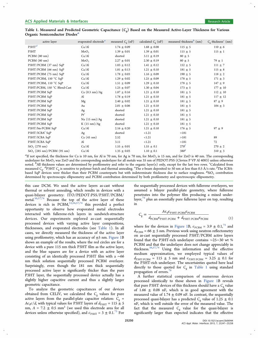
Table 1. Measured and Predicted Geometric Capacitance (Cg) Based on the Measured Active-Layer Thickness for VariousOrganic Semiconductor Diodesa
active layer evaporated electrodea measured Cg (nF) calculated Cg (nF) measured thicknessb (nm) Cg thicknessc (nm)
P3HTd Ca/Al 1.74 ± 0.09 1.68 ± 0.08 115 ± 5 110 ± 6P3HT MoO3 1.39 ± 0.01 1.39 ± 0.01 115 ± 5 115 ± 1PCBM (80 nm) Ca/Al shorted 3.11 ± 0.19 80 ± 5PCBM (80 nm) MoO3 2.27 ± 0.01 2.30 ± 0.19 80 ± 5 79 ± 1P3HT/PCBM (37 nm) SqP Ca/Al 1.83 ± 0.12 1.41 ± 0.12 152 ± 5 111 ± 7P3HT/PCBM (66 nm) SqP Ca/Al 1.81 ± 0.13 1.21 ± 0.10 181 ± 5 115 ± 8P3HT/PCBM (75 nm) SqP Ca/Al 1.78 ± 0.03 1.16 ± 0.09 190 ± 5 118 ± 2P3HT/PCBM, 150 °C SqP Ca/Al 1.29 ± 0.02 1.25 ± 0.09 178 ± 5 171 ± 3P3HT/PCBM, 110 °C SqP Ca/Al 1.51 ± 0.09 1.29 ± 0.10 178 ± 5 147 ± 9P3HT:PCBM, 150 °C Blend-Cast Ca/Al 1.25 ± 0.07 1.30 ± 0.04 173 ± 5 177 ± 10P3HT/PCBM SqP Ca (0.3 nm)/Ag 1.87 ± 0.16 1.21 ± 0.10 181 ± 5 112 ± 10P3HT/PCBM SqP Al 1.78 ± 0.19 1.21 ± 0.10 181 ± 5 117 ± 12P3HT/PCBM SqP Mg 2.40 ± 0.02 1.21 ± 0.10 181 ± 5 87 ± 9P3HT/PCBM SqP Au 2.01 ± 0.06 1.21 ± 0.10 181 ± 5 104 ± 3P3HT/PCBM SqP Ag shorted 1.21 ± 0.10 181 ± 5P3HT/PCBM SqP Pte shorted 1.21 ± 0.10 181 ± 5P3HT/PCBM SqP Na (15 nm)/Ag shorted 1.21 ± 0.10 181 ± 5P3HT/PCBM SqP K (15 nm)/Ag shorted 1.21 ± 0.10 181 ± 5P3HT/bis-PCBM SqP Ca/Al 2.16 ± 0.20 1.21 ± 0.10 176 ± 5 97 ± 9P3HT/ICBAf SqP Ag shorted <1.21 >181P3HT/ICBA SqP Ca (45 nm) 2.52 <1.21 >181 89P3HT/ICBA SqP Al 3.11 <1.21 >181 72SiO2 (270 nm) Ca/Al 1.55 ± 0.01 1.55 ± 0.1 270f 270 ± 2SiO2 (285 nm)/PCBM (95 nm) Ca/Al 1.35 ± 0.03 1.10 ± 0.1 380g 310 ± 3
aIf not specified, the thickness for Ca is 10 nm, for Al is 70 nm, for Ag is 70 nm, for MoO3 is 15 nm, and for ZnO is 40 nm. The correspondingunderlayer for MoO3 was ZnO and the corresponding underlayer for all metals was 35 nm of PEDOT:PSS (Clevios P VP Al 4083) unless otherwisenoted. bAll thickness values are determined by profilometry and refer to the organic layer(s) only, except for the last two rows. cCalculated frommeasured Cg.
dP3HT Cg is sensitive to polymer batch and thermal annealing.eThe e-beam deposited to 50 nm at less than 0.5 Å/s rate. fThe ICBA-
based SqP devices were thicker than their PCBM counterparts but with indeterminate thickness due to surface roughness. gSiO2 contributiondetermined by spectroscopic ellipsometry and PCBM contribution determined by both profilometry and spectroscopic ellipsometry.
ACS Applied Materials & Interfaces Research Article
DOI: 10.1021/acsami.5b06944ACS Appl. Mater. Interfaces 2015, 7, 25247−25258
25250
electrical thickness of the device is much thinner thananticipated, and in fact, this device has essentially the sameelectrical thickness as the original P3HT underlayer (Table 1).The only simple explanation for this discrepancy between the
measured and predicted Cg values is that in the quasi-bilayersamples, the evaporated Ca/Al electrode penetrates entirelythrough the PCBM-rich overlayer and only stops at the P3HT-rich interface, so that the quasi-bilayer Cg values becomeidentical to those of the pure underlayer. Despite the fact thatthe Cg values indicate that metal is penetrating a significantdistance into the organic layer, none of these devices in Figure1 were shorted or leaky, as evidenced by the roughly constantcurrent versus time, confirming that the metal does notpenetrate the entire organic layer. Table 1 presents measuredand predicted Cg values for a number of as-cast P3HT/PCBMSqP quasi-bilayer devices with different evaporated metalelectrodes (Ca/Al, Ca, Al, Mg, Ag, Pt, K, Na, and Au) andvarying PCBM overlayer thicknesses, all of which exhibitdiscrepancies between the measured and predicted geometriccapacitances that are consistent with significant metalpenetration into the active layers. In particular, the Cg valuesin Table 1 indicate that Au, Al, and Ca electrodes penetrateentirely through the fullerene-rich overlayer but not into theP3HT-rich underlayer, and that Ag, Mg, Pt, K, and Na canactually penetrate through the fullerene-rich overlayer and intothe P3HT-rich underlayer as well (Table 1). We note that thediffusion of alkali metals in polymers has been studied byothers,77 who argued that alkali metals ionize in contact withmost polymers and thus are highly mobile both becausepositive ions repel each other, preventing agglomeration of themetal, and because cations are smaller than neutral metalatoms. These ideas are consistent with the results of our Cganalysis.To evaluate how far the evaporated metal can penetrate
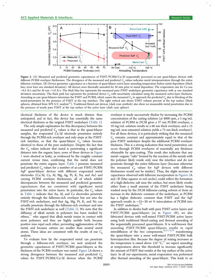
through a fullerene-rich overlayer, we next analyzed thegeometric capacitances of P3HT/PCBM quasi-bilayers as thethickness of the PCBM overlayer was varied. Figure 2A shows astrong divergence between the measured and predicted Cgvalues for P3HT/PCBM/Ca/Al devices when the PCBM
overlayer is made successively thicker by increasing the PCBMconcentration of the casting solution (at 4000 rpm, a 5 mg/mLsolution of PCBM in DCM gives a 37 nm PCBM overlayer, a10 mg/mL solution results in a 66 nm thick overlayer, and a 15mg/mL near-saturated solution yields a 75 nm thick overlayer).For all these devices, it is particularly striking that the measuredCg remains constant and approximately equal to that of thepure P3HT underlayer despite the additional PCBM overlayerthickness. This is a strong indication that metal penetration canoccur through PCBM overlayers of essentially any thicknessobtainable by spin-coating. This result also indicates that anymetal−organic “salts” formed by the reaction of the metals withthe polymer likely reside only near the interface and do notpenetrate through the entire fullerene layer (because otherwisethe measured Cg values for SqP devices with differentthicknesses would not be similar). Thus, the slight increase incapacitance observed with fullerene incorporation in Figures 2Aand 1B (blue squares vs red circles) could reflect the formationof a high-dielectric salt near the surface, but more likely resultseither from a small amount of the P3HT underlayer beingwashed away by the DCM fullerene-casting solvent or from anincrease in the dielectric constant of the underlayer, as PCBMhas a higher dielectric constant than P3HT and the SqPapproach results in ∼25−30 wt % intercalation of PCBM intothe P3HT underlayer.74
In addition to diodes built with pure P3HT active layers andP3HT/PCBM quasi-bilayers (as in Figure 1B), we alsofabricated devices with well-mixed P3HT:PCBM active layersusing both traditional blend-casting and thermal annealing ofthe sequentially processed quasi-bilayers. It is well-known thatannealing P3HT/PCBM quasi-bilayers results in rapidinterdiffusion of the two components,56,57,74,78 transformingthe quasi-bilayer into a more well-mixed P3HT:PCBM bulkheterojunction film. Because the degree of mixing increases asthe temperature is raised above 110 °C,57 we expect annealingat temperatures above this threshold to increase significantlythe amount of P3HT that resides at the top surface of the activelayer. In all our experiments, metal evaporation was performedafter thermal annealing of the quasi-bilayer. This leads to an
Figure 2. (A) Measured and predicted geometric capacitances of P3HT/PCBM/Ca/Al sequentially processed as-cast quasi-bilayer devices withdifferent PCBM overlayer thicknesses. The divergence of the measured and predicted Cg values indicates metal interpenetration through the entirefullerene overlayer. (B) Device geometric capacitance as a function of quasi-bilayer active-layer annealing temperature before metal deposition (blackline; error bars one standard deviation). All devices were thermally annealed for 20 min prior to metal deposition. The evaporation rate for Ca was∼0.5 Å/s and for Al was ∼1.0 Å/s. The thick blue bar represents the measured pure P3HT underlayer geometric capacitance with ± one standarddeviation uncertainty. The thick pink bar represents the predicted device Cg with uncertainty calculated using the measured active-layer thickness.Annealing as-cast quasi-bilayers intermixes the P3HT and PCBM, which causes the measured Cg to approach the predicted Cg due to blocking of themetal-penetration by the presence of P3HT at the top interface. The right vertical axis shows P3HT volume percent at the top surface (blackspheres; obtained from XPS S/C analysis68). Traditional blend-cast devices (dark cyan symbols) also show no measurable metal penetration due tothe presence of nearly pure P3HT at the top surface of the active layer (dark cyan sphere).
ACS Applied Materials & Interfaces Research Article
DOI: 10.1021/acsami.5b06944ACS Appl. Mater. Interfaces 2015, 7, 25247−25258
25251

expectation that the more annealed the film, the more P3HTwill cover the top surface, so less metal penetration shouldresult. Indeed, Figure 2B shows that the measured Cg ofannealed P3HT/PCBM quasi-bilayers steadily decreases withincreasing annealing temperature from 110 to 150 °C.Moreover, when the mixing becomes strong enough (byannealing for 20 min at 150 °C) the measured Cg becomes,within error, equal to the predicted Cg based on the measuredactive-layer thickness. Also plotted in Figure 2B is the Cg of ablend-cast P3HT:PCBM device that has the same totalthickness and composition as the quasi-bilayer devices.53 TheCg of this blend-cast device also shows no deviation betweenthe measured and predicted Cg values, consistent with the ideathat blend-casting produces devices with large amounts ofP3HT on the top surface.All of these results suggest that even small amounts of P3HT
at the top surface of the active layer can block metal penetrationin the same way that a P3HT-rich underlayer stops metalinterpenetration from completely shorting a quasi-bilayerdevice. To quantify better this effect, we measured the surfacecomposition of these active layers using X-ray photoelectronspectroscopy (XPS). For the P3HT/PCBM system, themeasured XPS sulfur/carbon ratio provides a direct measureof the amount of P3HT in the top few nanometers of the activelayer.53,68 The right vertical axis of Figure 2B shows the volumepercent of P3HT at the top surface of each of these samples asdetermined by XPS (see the Supporting Information for S/Ccalculation details). The data show that 150 °C-annealed quasi-bilayers and traditional blend-cast P3HT:PCBM active layershave >70 vol % P3HT at their top surfaces, whereas as-castP3HT/PCBM quasi-bilayers only have ∼3 vol % P3HT at theirsurfaces. Clearly, Figure 2B suggests that evaporated metalelectrodes can easily penetrate through fullerene-rich layers butcannot penetrate through even a small amount of diluteconjugated polymer such as P3HT. Taken together, the Cganalysis in Figures 1 and 2 and Table 1 leads to three majorconclusions: first, that the device geometric capacitance is areliable indicator of metal penetration; second, that thefunctional device structure is dramatically changed when anelectrode metal is evaporated onto a PCBM-rich layer; andthird, that P3HT acts as a remarkably efficient blocker of metalpenetration.
Because the presence of even small amounts of P3HT at thetop surface can affect metal penetration, it makes sense toinvestigate the interaction of evaporated metals with purefullerene films. Table 1 shows that when we fabricated diodeswith a pure PCBM active layer (device structure ITO/PEDOT:PSS/PCBM/Ca/Al), the devices were always eithershorted or too leaky to obtain reliable Cg values. This indicatesthat the evaporated electrode can effectively penetrate throughthe entire fullerene layer to make electrical contact with thebottom electrode, consistent with the quasi-bilayer resultsdiscussed above. To verify that there is nothing special aboutP3HT stopping metal interpenetration, Table 1 also summa-rizes results indicating metal penetration can be blocked byplacing a thin insulating interlayer (e.g., 15 nm of MoO3, whichis typically used to fabricate “inverted” OPV devices24,79) ontop of the fullerene layer; see also Figure S5 of the SupportingInformation. This observation might be an important reasonwhy inverted device architectures that utilize metal oxide bufferlayers typically work better than their normal-structurecounterparts for OPVs,79−81 as metal interpenetration couldeasily be detrimental to solar cell performance. Finally, Table 1also shows that we obtained identical Cg trends using otherfullerene derivatives, including indene-C60 bisadduct (ICBA)
82
and bis-PCBM,83 demonstrating that evaporated metal inter-penetration is a general phenomenon for many fullerenederivatives.As another way to investigate evaporated metal penetration
into pure fullerene films, we also fabricated devices using dopedSi with a thick thermal oxide overlayer as the bottom electrode.Table 1 shows that when a Ca/Al top electrode is evaporateddirectly onto the thick SiO2 thermal oxide layer, the measuredCg of the resulting device is in excellent agreement with theparallel-plate capacitor equation prediction: Cg = Aϵ0ϵSiO2
/dSiO2
= 1.55 nF, with dSiO2= 270 nm, ϵSiO2
= 3.9, and A = 12.1 mm2.However, when 95 nm of PCBM (as measured by profilometryand spectroscopic ellipsometry) is spun on top of the SiO2overlayer, the measured Cg is just 1.35 nF (with the same Ca/Altop electrode), which is much larger than that predicted andonly slightly smaller than that of the device built withoutPCBM. A simple analysis reveals that this Cg value accounts foronly ∼25 nm of the PCBM layer, leaving ∼70 nm of PCBM
Figure 3. Bright-field, cross-sectional TEM images of a glass/ITO/PEDOT:PSS/P3HT:PCBM/PCBM:Au/Au as-cast, sequentially processed quasi-bilayer device (the same device used in the Cg analysis in the previous section). (A) Representative section of the entire device stack and each layer’spersistence in the in-plane direction. (B) Higher magnification view of the P3HT:PCBM/PCBM:Au/Au interfaces, showing the clear formation ofmetal nanoparticles resulting from the thermal evaporation of Au onto the PCBM-rich portion of the active layer. (C) Further magnified view of theregion just above the interface with the P3HT-rich underlayer, showing a layer of fairly monodisperse ∼3.5 ± 0.5 nm diameter Au nanocrystals. Goldwas chosen as the electrode metal for these experiments due to its high Z-contrast with the organic layer and its stability in air. The evaporation ratefor the gold electrode was kept <0.5 Å/s.
ACS Applied Materials & Interfaces Research Article
DOI: 10.1021/acsami.5b06944ACS Appl. Mater. Interfaces 2015, 7, 25247−25258
25252
‘missing’ from the dielectric thickness. This demonstrates thatthe evaporated Au electrode has an effective electronicpenetration depth of approximately 70 nm into the 95 nmthick PCBM film. These data indicate that either the top 70 nmof the fullerene layer has become a part of the electrode or thatthe dielectric constant of this portion of the film has become sohigh because of the amount of intercalated metal that itessentially has no measurable capacitance when placed in serieswith the effective ∼25 nm of “pure” PCBM.3.2. X-TEM Analysis of Metal Interpenetration in
PCBM Films. With ample evidence in hand for metalpenetration, the obvious question becomes: can we directlyobserve and measure the infiltrated metal distribution insidethese fullerene layers? To address this question, we turn tocross-sectional transmission electron microscopy (X-TEM),where a focused-ion beam (FIB) is used to cut a thin sectionfrom an as-cast, sequentially processed P3HT/PCBM quasi-bilayer device, and the resulting device cross section is directlyimaged with TEM.21,52,84,85 To generate a sample for thisprocess, we evaporated a Au top electrode onto an as-castP3HT/PCBM quasi-bilayer active layer at a rate of only 0.1 Å/s, leading to an expected device architecture of glass/ITO (150nm)/PEDOT:PSS (35 nm)/P3HT:PCBM (130 nm)/PCBM(45 nm)/Au (50 nm); here, as above, we expect theP3HT:PCBM underlayer to have ∼25−30 wt % PCBM fromthe SqP.74 When collecting this data, care was taken to limitelectron beam exposure and any subsequent possible sampledamage.65,66,86 We note, however, that our primary interest inthis work is the structure of the interpenetrated metal, which isrobust to beam exposure. We chose to use gold as theevaporated top electrode material for three reasons: first, thecapacitance measurements described above indicate that Au canpenetrate up to ∼70 nm into fullerene-rich films; second, Auhas excellent Z-contrast in comparison to the carbon-basedP3HT/PCBM active-layer materials; and third, Au does notreadily degrade or oxidize, making it robust to the necessaryprocessing steps leading up to TEM imaging.Figure 3A clearly shows that instead of the nominally
fabricated glass/ITO/PEDOT:PSS/P3HT:PCBM/PCBM/Audevice structure, there is indeed readily visible Au metalpenetration into the PCBM overlayer. Further inspectionsuggests that a more accurate description of the actual devicearchitecture is glass/ITO/PEDOT:PSS/P3HT:PCBM/PCBM:Au/Au, with clear distinct boundaries for each of
these layers. We used high-angle annular dark-field (HAADF)scanning transmission electron microscopy (STEM), discussedbelow, and spot EDS spectra, shown in the SupportingInformation, to verify the elemental composition in eachregion of the image. One of the most striking and unexpectedfeatures of Figure 3A is a distinct layer of Au nanoparticles(NPs) that is visible ∼175 nm above the ITO/PEDOT:PSSinterface. This distance is consistent with the nominal thicknessof the P3HT-rich underlayer plus PEDOT:PSS interlayer,indicating that Au penetration proceeds all the way down to theP3HT-rich layer. This may seem surprising given that P3HThas a lower mass density than PCBM,87 but is in perfectagreement with the conclusions reached above from our Cganalysis. We hypothesize that the sulfur heteroatom in thepolymer plays a role in stopping metal penetration, becausegold, for example, has an otherwise high diffusivity inconjugated carbonaceous systems.58,59 In the P3HT/Ca system,for instance, it has been shown that the Ca/S-heteroatominteraction is significant enough to abstract the sulfur fromP3HT.88,89
Figure 3B focuses on what should have been the P3HT/PCBM quasi-bilayer interface,56,57,74 but instead is found to bea PCBM:Au-NP matrix in contact with the P3HT-richunderlayer. This image reveals that moving upward from theP3HT-rich underlayer interface, there is first a dense region ofsmall (∼3.5 nm diameter) Au NPs located at and just above theinterface, followed by a PCBM-rich region that contains verylittle Au, followed by a PCBM-rich layer that contains larger-sized (∼10−20 nm diameter) Au particles. Figure 3C showshigher magnification of the small Au NP layer just above theP3HT-rich interface, making clear that the spontaneouslyformed Au NPs are highly crystalline (see also the selected-areaelectron diffraction pattern in Figure S4 of the SupportingInformation). These particles are nominally spherical and fairlymonodisperse in size with diameters in the range of 3.5 ± 0.5nm. Not only is this type of NP formation at the bottom of athick organic layer extremely rare, but the pattern of small Aunanoparticles, pure organic layer, then larger Au NPs iscompletely different than that observed in previous inter-penetration studies.37 We postulate that the P3HT-richunderlayer has much to do with both the metal NP formationand distribution. There likely is a small amount of P3HT in thePCBM-rich overlayer (because SqP does mix the polymer andfullerene components, as indicated by the XPS data of Figure
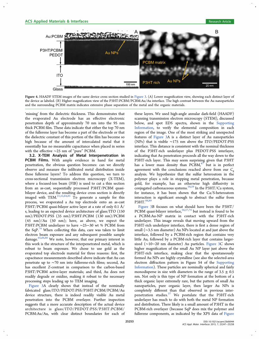
Figure 4. HAADF STEM images of the same device cross section studied in Figure 3. (A) Lower magnification view, showing each distinct layer ofthe device as labeled. (B) Higher magnification view of the P3HT:PCBM/PCBM:Au/Au interface. The high contrast between the Au nanoparticlesand the surrounding PCBM matrix indicates extensive phase separation of the metal and the organic materials.
ACS Applied Materials & Interfaces Research Article
DOI: 10.1021/acsami.5b06944ACS Appl. Mater. Interfaces 2015, 7, 25247−25258
25253
2).56,57 Given that P3HT interacts strongly with the penetratedmetal, it is entirely possible that the few P3HT chains dissolvedin the PCBM-rich overlayer act as nucleation sites for thepenetrated Au to grow into NPs, leading to the observednanostructure.3.3. HAADF X-TEM Analysis. To visualize better the
compositional nanostructure studied in Figure 3, we employedSTEM HAADF imaging of this same device cross section.HAADF STEM is not influenced by diffraction effects andprimarily reveals variations in atomic mass density (Z-contrast),making it ideal for examining the distribution of metallic Au inorganic matrices. As expected, the HAADF images in Figure 4show sharp contrast between the carbon-rich and gold-richregions of the Au:PCBM layer. Figure 4A shows the entireglass/ITO/PEDOT/P3HT:PCBM/PCBM:Au/Au layer stack,confirming that the layered structure of each region persiststhroughout the in-plane direction. Notably, there are several AuNPs visible as small gray dots in the P3HT-rich layer, althoughit is not clear whether these particles diffused into the layer viainterpenetration from above or were simply displaced duringthe FIB processing and are located on top of the cross-section.Figure 4A also better reveals the nonuniform Au:PCBMnanostructure seen in Figure 3A, which consists of a denseregion of small, ∼3.5 nm diameter gold NPs at the P3HT-richinterface, followed by a region devoid of Au, and then a thickerAu:PCBM matrix composed of large, semi-interconnected AuNPs (∼10−20 nm diameter). In Figure 4B, higher magnifica-tion HAADF imaging shows high contrast (i.e., a complete lackof gray scale) between the particles and surrounding matrix,indicating essentially complete phase separation of Au in thePCBM-rich layer. The formation of discrete Au nanoparticlessuggests that a significant contributor to the reduction of Cg, asdiscussed above, is the large increase in effective dielectricconstant of the mixed metal:fullerene layer, which causes thislayer to have no effective contribution to the overall devicecapacitance (eq 1 with ϵPCBM:Au → ∞).Overall, Figures 3 and 4 completely change our perception of
what can happen when evaporated electrode metals aredeposited onto layers rich in fullerene derivatives. The factthat electrode metals penetrate many tens of nanometers intofullerene-rich layers is not only unexpected but also will clearlyhave a significant impact on device optoelectronic properties.Although most of the effects are deleterious, it might bepossible to use the penetration to advantage, particularly if thesize of the intercalated NPs can be tuned, as we discuss in thenext section.3.4. Plasmonic Effects of Interpenetrated Nano-
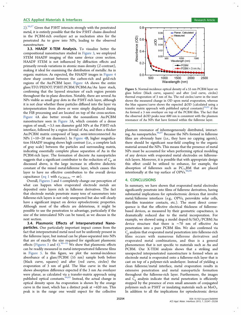
particles. One particularly important impact comes from thefact that interpenetrated metal need not be uniformly present inthe fullerene layer, but instead can be phase-separated into NPsthat are of exactly the size required for significant plasmoniceffects (Figures 3 and 4).90−93 We show that plasmonic effectscan be readily measured in metal-interpenetrated fullerene filmsin Figure 5. In this figure, we plot the normal-incidenceabsorbance of a glass/PCBM (55 nm) sample both before(black curve, squares) and after (red curve, circles) theevaporation of 3 nm of gold. The blue curve in the insetshows absorption difference expected if the 3 nm Au overlayerwere planar, as calculated via a transfer-matrix approach usingpublished optical constants.94,95 Instead, the actual change inoptical density upon Au evaporation is shown by the orangecurve in the inset, which has a distinct peak at ∼620 nm. Thispeak is in the range one would expect for the collective
plasmon resonance of inhomogeneously distributed, interact-ing, Au nanoparticles.96,97 Because the NPs formed in fullerenefilms are obviously bare (i.e., they have no capping agents),there should be significant near-field coupling to the organicmaterial around the NPs. This means that the presence of metalNPs must be accounted for when performing optical modelingof any devices with evaporated metal electrodes on fullerene-rich layers. Moreover, it is possible that with appropriate designthis effect could be utilized to enhance, for example, theabsorption of fullerenes such as PC71BM that are placedintentionally at the top surface of OPVs.90,98
4. CONCLUSIONSIn summary, we have shown that evaporated metal electrodessignificantly penetrate into films of fullerene derivatives, havingsubstantial implications for optoelectronic devices that involvemetal/fullerene interfaces (e.g., OPVs, perovskite solar cells,thin-film transistor contacts, etc.). The most direct conse-quence is that the effective electrical thickness of fullerene-based devices, as measured by their geometric capacitance, isdramatically reduced due to the metal incorporation. Forexample, we showed using a model doped-Si/SiO2/PCBM/Audevice structure that there is ∼70 nm of effective Aupenetration into a pure PCBM film. We also confirmed viaCg analysis that evaporated metal penetration into fullerene-richfilms occurs with numerous fullerene derivatives andevaporated metal combinations, and thus is a generalphenomenon that is not specific to materials such as Au andPCBM. Our X-TEM analysis shows that a striking andunexpected interpenetrated nanostructure is formed when anelectrode metal is evaporated onto a fullerene-rich layer that iscast on top of a polymer-rich underlayer. Instead of yielding aclean fullerene/metal interface, metal evaporation results inextensive penetration and metal nanoparticle formationthroughout the fullerene-rich layer. Furthermore, the imagesand Cg analysis indicate that metal penetration is efficientlystopped by the presence of even small amounts of conjugatedpolymers such as P3HT or insulating materials such as MoO3.In addition to all the implications for optoelectronic device
Figure 5. Normal-incidence optical density of a 55 nm PCBM layer onglass before (black curve, squares) and after (red curve, circles)thermal evaporation of 3 nm of Au. The red circles/curve in the insetshows the measured change in OD upon metal evaporation, whereasthe blue squares/curve shows the expected ΔOD (calculated using atransfer matrix approach with published optical constants)94,95 if theAu formed a 3 nm overlayer on top of the PCBM film. The fact thatthe observed ΔOD peaks near 600 nm is consistent with the plasmonresonance of Au NPs that have formed within the fullerene layer.
ACS Applied Materials & Interfaces Research Article
DOI: 10.1021/acsami.5b06944ACS Appl. Mater. Interfaces 2015, 7, 25247−25258
25254
physics experiments, this discovery opens up a number ofpossibilities in terms of interface and optical engineering withfullerene semiconductor materials.
■ ASSOCIATED CONTENT*S Supporting InformationThe Supporting Information is available free of charge on theACS Publications website at DOI: 10.1021/acsami.5b06944.
Details of the circuit modeling for determination of Cg,XPS analysis for determination of surface composition,EDS analysis of Au HAADF, selected-area electrondiffraction (SAED) on bright-field TEM images andCELIV result on pure PCBM devices with differentelectrodes (PDF).
■ AUTHOR INFORMATIONCorresponding Author*B. J. Schwartz. E-mail: [email protected] ContributionsG.Z. and S.A.H contributed equally to this work.NotesThe authors declare no competing financial interest.
■ ACKNOWLEDGMENTSThe authors thank Dr. Jia Ming Chen for ample administrativeassistance, Dr. Liane Slaughter for insightful discussions, NoahBodzin for making the X-TEM samples via FIB, and AmyFerreira for preparation of the Pt-based samples. This researchwas supported by the National Science Foundation under grantnumbers CHE-1510353 and CHE-1112569. The XPS instru-ment used in this work was obtained with support from theNSF, Award 0840531. J.C.A. and S.A.H. acknowledge previoussupport from the NSF IGERT: Materials Creation TrainingProgram (MCTP), grant number DGE-0654431 and theCalifornia NanoSystems Institute. C.N. acknowledges supportfrom the NSF (grant # CMMI-1200547). The authorsacknowledge the use of instruments at the Electron ImagingCenter for NanoMachines supported by NIH (1S10RR23057)and CNSI at UCLA.
■ REFERENCES(1) Jackson, N. E.; Savoie, B. M.; Marks, T. J.; Chen, L. X.; Ratner,M. A. The Next Breakthrough for Organic Photovoltaics? J. Phys.Chem. Lett. 2015, 6, 77−84.(2) Nelson, J. Polymer: Fullerene Bulk Heterojunction Solar Cells.Mater. Today 2011, 14, 462−470.(3) Gratzel, M. The Light and Shade of Perovskite Solar Cells. Nat.Mater. 2014, 13, 838−842.(4) Kim, H.-S.; Im, S. H.; Park, N.-G. Organolead Halide Perovskite:New Horizons in Solar Cell Research. J. Phys. Chem. C 2014, 118,5615−5625.(5) Hawks, S. A.; Deledalle, F.; Yao, J.; Rebois, D. G.; Li, G.; Nelson,J.; Yang, Y.; Kirchartz, T.; Durrant, J. R. Relating Recombination,Density of States, and Device Performance in an Efficient Polymer:-Fullerene Organic Solar Cell Blend. Adv. Energy Mater. 2013, 3, 1201−1209.(6) Hawks, S. A.; Li, G.; Yang, Y.; Street, R. A. Band TailRecombination in Polymer:Fullerene Organic Solar Cells. J. Appl. Phys.2014, 116, 074503.(7) Street, R. A.; Hawks, S. A.; Khlyabich, P. P.; Li, G.; Schwartz, B.J.; Thompson, B. C.; Yang, Y. Electronic Structure and TransitionEnergies in Polymer-Fullerene Bulk Heterojunctions. J. Phys. Chem. C2014, 118, 21873−21883.
(8) Aguirre, J. C.; Arntsen, C.; Hernandez, S.; Huber, R.; Nardes, A.M.; Halim, M.; Kilbride, D.; Rubin, Y.; Tolbert, S. H.; Kopidakis, N.;Schwartz, B. J.; Neuhauser, D. Understanding Local and MacroscopicElectron Mobilities in the Fullerene Network of Conjugated Polymer-based Solar Cells: Time-Resolved Microwave Conductivity andTheory. Adv. Funct. Mater. 2014, 24, 784−792.(9) Vandewal, K.; Albrecht, S.; Hoke, E. T.; Graham, K. R.; Widmer,J.; Douglas, J. D.; Schubert, M.; Mateker, W. R.; Bloking, J. T.;Burkhard, G. F.; Sellinger, A.; Frechet, J. M. J.; Amassian, A.; Riede, M.K.; McGehee, M. D.; Neher, D.; Salleo, A. Efficient Charge Generationby Relaxed Charge-Transfer States at Organic Interfaces. Nat. Mater.2013, 13, 63−68.(10) Mei, A.; Li, X.; Liu, L.; Ku, Z.; Liu, T.; Rong, Y.; Xu, M.; Hu, M.;Chen, J.; Yang, Y.; Gratzel, M.; Han, H. A Hole-Conductor-Free, FullyPrintable Mesoscopic Perovskite Solar Cell with High Stability. Science2014, 345, 295−298.(11) Tremolet De Villers, B.; Tassone, C. J.; Tolbert, S. H.; Schwartz,B. J. Improving the Reproducibility of P3HT:PCBM Solar Cells byControlling the PCBM/Cathode Interface. J. Phys. Chem. C 2009, 113,18978−18982.(12) Finck, B. Y.; Schwartz, B. J. Understanding the Origin of the S-Curve in Conjugated Polymer/Fullerene Photovoltaics from Drift-Diffusion Simulations. Appl. Phys. Lett. 2013, 103, 053306.(13) Campoy-Quiles, M.; Ferenczi, T.; Agostinelli, T.; Etchegoin, P.G.; Kim, Y.; Anthopoulos, T. D.; Stavrinou, P. N.; Bradley, D. D. C.;Nelson, J. Morphology Evolution via Self-Organization and Lateral andVertical Diffusion in Polymer: Fullerene Solar Cell Blends. Nat. Mater.2008, 7, 158−164.(14) Liu, Y.; Liu, F.; Wang, H. W. H.-W.; Nordlund, D.; Sun, Z.;Ferdous, S.; Russell, T. P. Sequential Deposition: Optimization ofSolvent Swelling for High-Performance Polymer Solar Cells. ACSAppl. Mater. Interfaces 2015, 7, 653−661.(15) Yu, Z.; Sun, L. Recent Progress on Hole-Transporting Materialsfor Emerging Organometal Halide Perovskite Solar Cells. Adv. EnergyMater. 2015, 5, 1500213.(16) Wetzelaer, G.-J. A. H.; Scheepers, M.; Sempere, A. M.;Momblona, C.; Avila, J.; Bolink, H. J. Trap-Assisted Non-RadiativeRecombination in Organic-Inorganic Perovskite Solar Cells. Adv.Mater. 2015, 27, 1837−1841.(17) Zhang, Y.; Liu, M.; Eperon, G. E.; Leijtens, T. C.; McMeekin,D.; Saliba, M.; Zhang, W.; de Bastiani, M.; Petrozza, A.; Herz, L. M.;Johnston, M. B.; Lin, H.; Snaith, H. J. Charge Selective Contacts,Mobile Ions and Anomalous Hysteresis in Organic-Inorganic Perov-skite Solar Cells. Mater. Horiz. 2015, 2, 315−322.(18) Ratcliff, E. L.; Garcia, A.; Paniagua, S. A.; Cowan, S. R.;Giordano, A. J.; Ginley, D. S.; Marder, S. R.; Berry, J. J.; Olson, D. C.Investigating the Influence of Interfacial Contact Properties on OpenCircuit Voltages in Organic Photovoltaic Performance: Work FunctionVersus Selectivity. Adv. Energy Mater. 2013, 3, 647−656.(19) Heo, J. H.; Im, S. H.; Noh, J. H.; Mandal, T. N.; Lim, C.-S.;Chang, J. A.; Lee, Y. H.; Kim, H.-j.; Sarkar, A.; Nazeeruddin, Md. K.;Gratzel, M.; Seok, S. I. Efficient Inorganic-Organic HybridHeterojunction Solar Cells Containing Perovskite Compound andPolymeric Hole Conductors. Nat. Photonics 2013, 7, 486−491.(20) Jeon, N. J.; Noh, J. H.; Yang, W. S.; Kim, Y. C.; Ryu, S.; Seo, J.;Seok, S. I. Compositional Engineering of Perovskite Materials forHigh-Performance Solar Cells. Nature 2015, 517, 476−480.(21) Chen, D.; Nakahara, A.; Wei, D.; Nordlund, D.; Russell, T. P.P3HT/PCBM Bulk Heterojunction Organic Photovoltaics: Correlat-ing Efficiency and Morphology. Nano Lett. 2011, 11, 561−567.(22) Seok, J.; Shin, T. J.; Park, S.; Cho, C.; Lee, J.-Y.; Yeol Ryu, D.;Kim, M. H.; Kim, K. Efficient Organic Photovoltaics UtilizingNanoscale Heterojunctions in Sequentially Deposited Polymer/fullerene Bilayer. Sci. Rep. 2015, 5, 8373.(23) Roehling, J. D.; Rochester, C. W.; Ro, H. W.; Wang, P.;Majewski, J.; Batenburg, K. J.; Arslan, I.; Delongchamp, D. M.; Moule,A. J. Material Profile Influences in Bulk-Heterojunctions. J. Polym. Sci.,Part B: Polym. Phys. 2014, 52, 1291−1300.
ACS Applied Materials & Interfaces Research Article
DOI: 10.1021/acsami.5b06944ACS Appl. Mater. Interfaces 2015, 7, 25247−25258
25255

(24) Mauger, S. A.; Chang, L.; Friedrich, S.; Rochester, C. W.;Huang, D. M.; Wang, P.; Moule, A. J. Self-Assembly of SelectiveInterfaces in Organic Photovoltaics. Adv. Funct. Mater. 2013, 23,1935−1946.(25) Tseng, W.-H.; Lo, H.; Chang, J.-K.; Liu, I.-H.; Chen, M.-H.; Wu,C.-I. Metal-Induced Molecular Diffusion in [6,6]-Phenyl-C61-ButyricAcid Methyl Ester Poly(3-hexylthiophene) Based Bulk-HeterojunctionSolar Cells. Appl. Phys. Lett. 2013, 103, 183506.(26) Wertheim, G. K.; Buchanan, D. N. E. Reaction of C60 withMetals: W. Solid State Commun. 1993, 88, 97−100.(27) Chikamatsu, M.; Taima, T.; Yoshida, Y.; Saito, K.; Yase, K. Mg-Doped C60 Thin Film as Improved N-Type Organic Semiconductorfor A Solar Cell. Appl. Phys. Lett. 2004, 84, 127−129.(28) Wang, H.; Hou, J. G.; Takeuchi, O.; Fujisuku, Y.; Kawazu, A.STM Observations of Ag-Induced Reconstruction of C60 Thin Films.Phys. Rev. B: Condens. Matter Mater. Phys. 2000, 61, 2199−2203.(29) Devenyi, A.; Manaila, R.; Belu-Marian, A. Nanocrystalline Goldin Au-Doped Thin C60 Films. Thin Solid Films 1998, 335, 258−265.(30) Matz, D. L.; Ratcliff, E. L.; Meyer, J.; Kahn, A.; Pemberton, J. E.Deciphering the Metal-C60 Interface in Optoelectronic Devices:Evidence for C60 Reduction by Vapor Deposited Al. ACS Appl. Mater.Interfaces 2013, 5, 6001−6008.(31) Shukla, M. K.; Dubey, M.; Leszczynski, J. TheoreticalInvestigation of Electronic Structures and Properties of C60-GoldNanocontacts. ACS Nano 2008, 2, 227−234.(32) Tondelier, D.; Lmimouni, K.; Vuillaume, D.; Fery, C.; Haas, G.Metal/Organic/Metal Bistable Memory Devices. Appl. Phys. Lett.2004, 85, 5763−5765.(33) Scharnberg, M.; Adelung, R.; Faupel, F. Influence of Top LayerGeometries on the Electronic Properties of Pentacene andDiindenoperylene Thin Films. Phys. Status Solidi A 2008, 205, 578−590.(34) Zhang, X. H.; Domercq, B.; Kippelen, B. Effect of AuDeposition Rate on the Performance of Top-Contact PentaceneOrganic Field-Effect Transistors. Synth. Met. 2009, 159, 2371−2374.(35) Fladischer, S.; Neuhold, A.; Kraker, E.; Haber, T.; Lamprecht,B.; Salzmann, I.; Resel, R.; Grogger, W. Diffusion of Ag into OrganicSemiconducting Materials: A Combined Analytical Study UsingTransmission Electron Microscopy and X-Ray Reflectivity. ACSAppl. Mater. Interfaces 2012, 4, 5608−5612.(36) Yu, S.; Santoro, G.; Sarkar, K.; Dicke, B.; Wessels, P.; Bommel,S.; Dohrmann, R.; Perlich, J.; Kuhlmann, M.; Metwalli, E.; Risch, J. F.H.; Schwartzkopf, M.; Drescher, M.; Muller-Buschbaum, P.; Roth, S.V. Formation of Al Nanostructures on Alq3: An In situ GrazingIncidence Small Angle X-Ray Scattering Study During RadioFrequency Sputter Deposition. J. Phys. Chem. Lett. 2013, 4, 3170−3175.(37) Durr, A. C.; Schreiber, F.; Kelsch, M.; Carstanjen, H. D.; Dosch,H.; Seeck, O. H. Morphology and Interdiffusion Behavior ofEvaporated Metal Films on Crystalline Diindenoperylene ThinFilms. J. Appl. Phys. 2003, 93, 5201−5209.(38) Schwartzkopf, M.; Santoro, G.; Brett, C. J.; Rothkirch, A.;Polonskyi, O.; Hinz, A.; Metwalli, E.; Yao, Y.; Strunskus, T.; Faupel, F.;Muller-Buschbaum, P.; Roth, S. V. Real-Time Monitoring ofMorphology and Optical Properties during Sputter Deposition forTailoring Metal-Polymer Interfaces. ACS Appl. Mater. Interfaces 2015,7, 13547−13556.(39) Kirchartz, T.; Agostinelli, T.; Campoy-Quiles, M.; Gong, W.;Nelson, J. Understanding the Thickness-Dependent Performance ofOrganic Bulk Heterojunction Solar Cells: The Influence of Mobility,Lifetime, and Space Charge. J. Phys. Chem. Lett. 2012, 3, 3470−3475.(40) Hawks, S. A.; Finck, B. Y.; Schwartz, B. J. Theory of CurrentTransients in Planar Semiconductor Devices: Insights and Applicationsto Organic Solar Cells. Phys. Rev. Appl. 2015, 3, 44014.(41) Natali, D.; Caironi, M. Charge Injection in Solution-ProcessedOrganic Field-Effect Transistors: Physics, Models and CharacterizationMethods. Adv. Mater. 2012, 24, 1357−1387.(42) Dongaonkar, S.; Servaites, J. D.; Ford, G. M.; Loser, S.; Moore,J.; Gelfand, R. M.; Mohseni, H.; Hillhouse, H. W.; Agrawal, R.; Ratner,
M. a.; Marks, T. J.; Lundstrom, M. S.; Alam, M. A. Universality ofNon-Ohmic Shunt Leakage in Thin-Film Solar Cells. J. Appl. Phys.2010, 108, 124509.(43) Wagner, J.; Gruber, M.; Wilke, A.; Tanaka, Y.; Topczak, K.;Steindamm, A.; Hormann, U.; Opitz, A.; Nakayama, Y.; Ishii, H.;Pflaum, J.; Koch, N.; Brutting, W. Identification of Different Originsfor S-Shaped Current Voltage Characteristics in Planar HeterojunctionOrganic Solar Cells. J. Appl. Phys. 2012, 111, 054509.(44) Steindamm, A.; Brendel, M.; Topczak, a. K.; Pflaum, J.Thickness Dependent Effects of An Intermediate Molecular BlockingLayer on the Optoelectronic Characteristics of Organic BilayerPhotovoltaic Cells. Appl. Phys. Lett. 2012, 101, 143302.(45) Dibb, G. F. A.; Muth, M.-A.; Kirchartz, T.; Engmann, S.; Hoppe,H.; Gobsch, G.; Thelakkat, M.; Blouin, N.; Tierney, S.; Carrasco-Orozco, M.; Durrant, J. R.; Nelson, J. Influence of Doping on ChargeCarrier Collection in Normal and Inverted Geometry Polymer:-Fullerene Solar Cells. Sci. Rep. 2013, 3, 1−7.(46) Bisquert, J.; Kirchartz, T.; Mora-Sero, I.; Garcia-Belmonte, G.Classification of Solar Cells According to Mechanisms of ChargeSeparation and Charge Collection. Phys. Chem. Chem. Phys. 2015, 17,4007−4014.(47) Reese, M. O.; White, M. S.; Rumbles, G.; Ginley, D. S.;Shaheen, S. E. Optimal Negative Electrodes for Poly(3-Hexylth-iophene): 6,6-Phenyl C61-Butyric Acid Methyl Ester Bulk Hetero-junction Photovoltaic Devices. Appl. Phys. Lett. 2008, 92, 053307.(48) Amarandei, G.; Clancy, I.; Arshak, A.; Corcoran, D. Stability ofUltrathin Nanocomposite Polymer Films Controlled by theEmbedding of Gold Nanoparticles. ACS Appl. Mater. Interfaces 2014,6, 20758−20767.(49) Chen, H.; Hsiao, Y.-C.; Hu, B.; Dadmun, M. Control ofMorphology and Function of Low Band Gap Polymer-Bis-FullereneMixed Heterojunctions in Organic Photovoltaics with SelectiveSolvent Vapor Annealing. J. Mater. Chem. A 2014, 2, 9883−9890.(50) Huang, J.-H.; Hsiao, Y.-S.; Richard, E.; Chen, C.-C.; Chen, P.;Li, G.; Chu, C.-W.; Yang, Y. The Investigation of Donor-AcceptorCompatibility in Bulk-Heterojunction Polymer Systems. Appl. Phys.Lett. 2013, 103, 043304.(51) Parnell, A. J.; Dunbar, A. D. F.; Pearson, A. J.; Staniec, P. A.;Dennison, A. J. C.; Hamamatsu, H.; Skoda, M. W. A.; Lidzey, D. G.;Jones, R. A. L. Depletion of PCBM at the Cathode Interface in P3HT/PCBM Thin Films as Quantified via Neutron Reflectivity Measure-ments. Adv. Mater. 2010, 22, 2444−2447.(52) Ayzner, A. L.; Tassone, C. J.; Tolbert, S. H.; Schwartz, B. J.Reappraising the Need for Bulk Heterojunctions in Polymer-FullerenePhotovoltaics: The Role of Carrier Transport in All-Solution-Processed P3HT/PCBM Bilayer Solar Cells. J. Phys. Chem. C 2009,113, 20050−20060.(53) Hawks, S. A.; Aguirre, J. C.; Schelhas, L. T.; Thompson, R. J.;Huber, R. C.; Ferreira, A. S.; Zhang, G.; Herzing, A. A.; Tolbert, S. H.;Schwartz, B. J. Comparing Matched Polymer:Fullerene Solar CellsMade by Solution-Sequential Processing and Traditional BlendCasting: Nanoscale Structure and Device Performance. J. Phys.Chem. C 2014, 118, 17413−17425.(54) Zhang, G.; Huber, R. C.; Ferreira, A. S.; Boyd, S. D.; Luscombe,C. K.; Tolbert, S. H.; Schwartz, B. J. Crystallinity Effects inSequentially Processed and Blend-Cast Bulk-Heterojunction Poly-mer/Fullerene Photovoltaics. J. Phys. Chem. C 2014, 118, 18424−18435.(55) Aguirre, J. C.; Hawks, S. A.; Ferreira, A. S.; Yee, P.;Subramaniyan, S.; Jenekhe, S. A.; Tolbert, S. H.; Schwartz, B. J.Sequential Processing for Organic Photovoltaics: Design Rules forMorphology Control by Tailored Semi-Orthogonal Solvent Blends.Adv. Energy Mater. 2015, 5, 1402020.(56) Lee, K. H.; Schwenn, P. E.; Smith, A. R. G.; Cavaye, H.; Shaw, P.E.; James, M.; Krueger, K. B.; Gentle, I. R.; Meredith, P.; Burn, P. L.Morphology of All-Solution-Processed ”Bilayer” Organic Solar Cells.Adv. Mater. 2011, 23, 766−770.(57) Lee, K. H.; Zhang, Y.; Burn, P. L.; Gentle, I. R.; James, M.;Nelson, A.; Meredith, P. Correlation of Diffusion and Performance in
ACS Applied Materials & Interfaces Research Article
DOI: 10.1021/acsami.5b06944ACS Appl. Mater. Interfaces 2015, 7, 25247−25258
25256

Sequentially Processed P3HT/PCBM Heterojunction Films by Time-Resolved Neutron Reflectometry. J. Mater. Chem. C 2013, 1, 2593−2598.(58) Tomita, Y.; Nakayama, T. In Electron. Process. Org. Electron.;Ishii, H., Kudo, K., Nakayama, T., Ueno, N., Eds.; Springer Series inMaterials Science; Springer Japan: Tokyo, 2015; Chapter 14, pp 303−317.(59) Tomita, Y.; Nakayama, T. Metal-Atom Diffusion in OrganicSolids: First-Principles Study of Graphene and Polyacetylene Systems.Appl. Phys. Express 2010, 3, 091601.(60) Abrusci, A.; Stranks, S. D.; Docampo, P.; Yip, H.-L.; Jen, A. K.-Y.; Snaith, H. J. High-Performance Perovskite-Polymer Hybrid SolarCells via Electronic Coupling with Fullerene Monolayers. Nano Lett.2013, 13, 3124−3128.(61) Shao, Y.; Xiao, Z.; Bi, C.; Yuan, Y.; Huang, J. Origin andElimination of Photocurrent Hysteresis by Fullerene Passivation inCH3NH3PbI3 Planar Heterojunction Solar Cells. Nat. Commun.2014, 5, 5784.(62) Jeng, J.-Y.; Chiang, Y.-F.; Lee, M.-H.; Peng, S.-R.; Guo, T.-F.;Chen, P.; Wen, T.-C. CH3NH3PbI3 Perovskite/Fullerene Planar-Heterojunction Hybrid Solar Cells. Adv. Mater. 2013, 25, 3727−3732.(63) Ayzner, A. L.; Wanger, D. D.; Tassone, C. J.; Tolbert, S. H.;Schwartz, B. J. Room to Improve Conjugated Polymer-Based SolarCells: Understanding How Thermal Annealing Affects the FullereneComponent of a Bulk Heterojunction Photovoltaic Device. J. Phys.Chem. C 2008, 112, 18711−18716.(64) Beek, W. J. E.; Wienk, M. M.; Kemerink, M.; Yang, X.; Janssen,R. A. J. Hybrid Zinc Oxide Conjugated Polymer Bulk HeterojunctionSolar Cells. J. Phys. Chem. B 2005, 109, 9505−9516.(65) Takacs, C. J.; Treat, N. D.; Kramer, S.; Chen, Z.; Facchetti, A.;Chabinyc, M. L.; Heeger, A. J. Remarkable Order of A High-Performance Polymer. Nano Lett. 2013, 13, 2522−2527.(66) Egerton, R. F.; Li, P.; Malac, M. Radiation Damage in the TEMand SEM. Micron 2004, 35, 399−409.(67) Herzing, A. A.; Ro, H. W.; Soles, C. L.; DeLongchamp, D. M.Visualization of Phase Evolution in Model Organic PhotovoltaicStructures via Energy-Filtered Transmission Electron Microscopy.ACS Nano 2013, 7, 7937−7944.(68) Cheng, P.; Hou, J.; Li, Y.; Zhan, X. Layer-by-Layer Solution-Processed Low-Bandgap Polymer-PC61BM Solar Cells with HighEfficiency. Adv. Energy Mater. 2014, 4, 1301349.(69) Juska, G.; Arlauskas, K.; Viliu nas, M. Charge Transport in π-Conjugated Polymers from Extraction Current Transients. Phys. Rev.B: Condens. Matter Mater. Phys. 2000, 62, 235−238.(70) Bange, S.; Schubert, M.; Neher, D. Charge MobilityDetermination by Current Extraction under Linear IncreasingVoltages: Case of Nonequilibrium Charges and Field-DependentMobilities. Phys. Rev. B: Condens. Matter Mater. Phys. 2010, 81, 35209.(71) Sandberg, O. J.; Nyman, M.; Osterbacka, R. DirectDetermination of Doping Concentration and Built-in Voltage fromExtraction Current Transients. Org. Electron. 2014, 15, 3413−3420.(72) Armin, A.; Juska, G.; Philippa, B. W.; Burn, P. L.; Meredith, P.;White, R. D.; Pivrikas, A. Doping-Induced Screening of the Built-in-Field in Organic Solar Cells: Effect on Charge Transport andRecombination. Adv. Energy Mater. 2013, 3, 321−327.(73) van Franeker, J. J.; Kouijzer, S.; Lou, X.; Turbiez, M.; Wienk, M.M.; Janssen, R. A. J. Depositing Fullerenes in Swollen Polymer Layersvia Sequential Processing of Organic Solar Cells. Adv. Energy Mater.2015, 5, 1500464.(74) Rochester, C. W.; Mauger, S. A.; Moule, A. J. Investigating theMorphology of Polymer/Fullerene Layers Coated Using OrthogonalSolvents. J. Phys. Chem. C 2012, 116, 7287−7292.(75) Liu, T.; Troisi, A. Absolute Rate of Charge Separation andRecombination in a Molecular Model of the P3HT/PCBM Interface. J.Phys. Chem. C 2011, 115, 2406−2415.(76) Taylor, J. R. An Introduction to Error Analysis, the Study ofUncertainties in Physical Measurements, 2nd ed.;University ScienceBooks: Sausalito, CA, 1997.
(77) Gupta, D. Diffusion Processes in Advanced Technological Materials;William Andrew, Inc.: Norwich, NY, 2005; Chapter 7, pp 333−363.(78) Treat, N. D.; Brady, M. A.; Smith, G.; Toney, M. F.; Kramer, E.J.; Hawker, C. J.; Chabinyc, M. L. Interdiffusion of PCBM and P3HTReveals Miscibility in a Photovoltaically Active Blend. Adv. EnergyMater. 2011, 1, 82−89.(79) Li, G.; Chu, C. W.; Shrotriya, V.; Huang, J.; Yang, Y. EfficientInverted Polymer Solar Cells. Appl. Phys. Lett. 2006, 88, 253503.(80) You, J.; Chen, C.-C.; Dou, L.; Murase, S.; Duan, H.-S.; Hawks,S. A.; Xu, T.; Son, H. J.; Yu, L.; Li, G.; Yang, Y. Metal OxideNanoparticles as an Electron-Transport Layer in High-Performanceand Stable Inverted Polymer Solar Cells. Adv. Mater. 2012, 24, 5267−5272.(81) He, Z.; Zhong, C.; Su, S.; Xu, M.; Wu, H.; Cao, Y. EnhancedPower-Conversion Efficiency in Polymer Solar Cells Using an InvertedDevice Structure. Nat. Photonics 2012, 6, 593−597.(82) Zhao, G.; He, Y.; Li, Y. 6.5% Efficiency of Polymer Solar CellsBased on Poly(3-Hexylthiophene) and Indene-C(60) Bisadduct byDevice Optimization. Adv. Mater. 2010, 22, 4355−4358.(83) He, Y.; Chen, H. Y.; Hou, J.; Li, Y. Indene-C60 Bisadduct: ANew Acceptor for High-Performance Polymer Solar Cells. J. Am.Chem. Soc. 2010, 132, 1377−1382.(84) Steuerman, D. W.; Garcia, a.; Dante, M.; Yang, R.; Lofvander, J.P.; Nguyen, T.-Q. Imaging the Interfaces of Conjugated PolymerOptoelectronic Devices. Adv. Mater. 2008, 20, 528−534.(85) Wang, D. H.; Moon, J. S.; Seifter, J.; Jo, J.; Park, J. H.; Park, O.O.; Heeger, A. J. Sequential Processing: Control of Nanomorphologyin Bulk Heterojunction Solar Cells. Nano Lett. 2011, 11, 3163−3168.(86) Sun, Y.; Welch, G. C.; Leong, W. L.; Takacs, C. J.; Bazan, G. C.;Heeger, A. J. Solution-Processed Small-Molecule Solar Cells with 6.7%Efficiency. Nat. Mater. 2011, 11, 44−48.(87) Machui, F.; Rathgeber, S.; Li, N.; Ameri, T.; Brabec, C. J.Influence of a Ternary Donor Material on the Morphology of aP3HT:PCBM Blend for Organic Photovoltaic Devices. J. Mater. Chem.2012, 22, 15570−15577.(88) Bebensee, F.; Schmid, M.; Steinruck, H.-P.; Campbell, C. T.;Gottfried, J. M. Toward Well-Defined Metal-Polymer Interfaces:Temperature-Controlled Suppression of Subsurface Diffusion andReaction at the Calcium/Poly(3-hexylthiophene) Interface. J. Am.Chem. Soc. 2010, 132, 12163−12165.(89) Bebensee, F.; Zhu, J.; Baricuatro, J. H.; Farmer, J. A.; Bai, Y.;Steinruck, H.-P.; Campbell, C. T.; Gottfried, J. M. Interface Formationbetween Calcium and Electron-Irradiated Poly(3-hexylthiophene).Langmuir 2010, 26, 9632−9639.(90) Atwater, H. A.; Polman, A. Plasmonics for ImprovedPhotovoltaic Devices. Nat. Mater. 2010, 9, 205−213.(91) Gan, Q.; Bartoli, F. J.; Kafafi, Z. H. Plasmonic-EnhancedOrganic Photovoltaics: Breaking the 10% Efficiency Barrier. Adv.Mater. 2013, 25, 2385−2396.(92) Xue, M.; Li, L.; Tremolet De Villers, B. J.; Shen, H.; Zhu, J.; Yu,Z.; Stieg, A. Z.; Pei, Q.; Schwartz, B. J.; Wang, K. L. Charge-CarrierDynamics in Hybrid Plasmonic Organic Solar Cells with AgNanoparticles. Appl. Phys. Lett. 2011, 98, 253302.(93) Ahn, S.; Jang, W.; Park, J. H.; Wang, D. H. EnhancedPerformance of Layer-Evolved Bulk-Heterojunction Solar Cells withAg Nanoparticles by Sequential Deposition. Org. Electron. 2015, 24,325−329.(94) Burkhard, G. F.; Hoke, E. T.; McGehee, M. D. Accounting forInterference, Scattering, and Electrode Absorption to Make AccurateInternal Quantum Efficiency Measurements in Organic and OtherThin Solar Cells. Adv. Mater. 2010, 22, 3293−3297.(95) Peumans, P.; Yakimov, A.; Forrest, S. R. Small MolecularWeight Organic Thin-Film Photodetectors and Solar Cells. J. Appl.Phys. 2003, 93, 3693−3723.(96) Ghosh, S. K.; Pal, T. Interparticle Coupling Effect on theSurface Plasmon Resonance of Gold Nanoparticles: From Theory toApplications. Chem. Rev. 2007, 107, 4797−4862.
ACS Applied Materials & Interfaces Research Article
DOI: 10.1021/acsami.5b06944ACS Appl. Mater. Interfaces 2015, 7, 25247−25258
25257

(97) Geng, M.; Zhang, Y.; Huang, Q.; Zhang, B.; Li, Q.; Li, W.; Li, J.Functionalization of C60 with Gold Nanoparticles. Carbon 2010, 48,3570−3574.(98) Yip, H.-L.; Jen, A. K.-Y. Recent Advances in Solution-ProcessedInterfacial Materials for Efficient and Stable Polymer Solar Cells.Energy Environ. Sci. 2012, 5, 5994−6011.
ACS Applied Materials & Interfaces Research Article
DOI: 10.1021/acsami.5b06944ACS Appl. Mater. Interfaces 2015, 7, 25247−25258
25258