f 'ònÛ7± w 7§ ¸à Á&âÎ oæ,¬¥f @ù×e Ðneªuzc qÍý ±Â12§ · title: ws~ô...
TRANSCRIPT

To learn more about ON Semiconductor, please visit our website at www.onsemi.com
Please note: As part of the Fairchild Semiconductor integration, some of the Fairchild orderable part numbers will need to change in order to meet ON Semiconductor’s system requirements. Since the ON Semiconductor product management systems do not have the ability to manage part nomenclature that utilizes an underscore (_), the underscore (_) in the Fairchild part numbers will be changed to a dash (-). This document may contain device numbers with an underscore (_). Please check the ON Semiconductor website to verify the updated device numbers. The most current and up-to-date ordering information can be found at www.onsemi.com. Please email any questions regarding the system integration to [email protected].
Is Now Part of
ON Semiconductor and the ON Semiconductor logo are trademarks of Semiconductor Components Industries, LLC dba ON Semiconductor or its subsidiaries in the United States and/or other countries. ON Semiconductor owns the rights to a number of patents, trademarks, copyrights, trade secrets, and other intellectual property. A listing of ON Semiconductor’s product/patent coverage may be accessed at www.onsemi.com/site/pdf/Patent-Marking.pdf. ON Semiconductor reserves the right to make changes without further notice to any products herein. ON Semiconductor makes no warranty, representation or guarantee regarding the suitability of its products for any particular purpose, nor does ON Semiconductor assume any liability arising out of the application or use of any product or circuit, and specifically disclaims any and all liability, including without limitation special, consequential or incidental damages. Buyer is responsible for its products and applications using ON Semiconductor products, including compliance with all laws, regulations and safety requirements or standards, regardless of any support or applications information provided by ON Semiconductor. “Typical” parameters which may be provided in ON Semiconductor data sheets and/or specifications can and do vary in different applications and actual performance may vary over time. All operating parameters, including “Typicals” must be validated for each customer application by customer’s technical experts. ON Semiconductor does not convey any license under its patent rights nor the rights of others. ON Semiconductor products are not designed, intended, or authorized for use as a critical component in life support systems or any FDA Class 3 medical devices or medical devices with a same or similar classification in a foreign jurisdiction or any devices intended for implantation in the human body. Should Buyer purchase or use ON Semiconductor products for any such unintended or unauthorized application, Buyer shall indemnify and hold ON Semiconductor and its officers, employees, subsidiaries, affiliates, and distributors harmless against all claims, costs, damages, and expenses, and reasonable attorney fees arising out of, directly or indirectly, any claim of personal injury or death associated with such unintended or unauthorized use, even if such claim alleges that ON Semiconductor was negligent regarding the design or manufacture of the part. ON Semiconductor is an Equal Opportunity/Affirmative Action Employer. This literature is subject to all applicable copyright laws and is not for resale in any manner.
August 2016
© 2016 Fairchild Semiconductor Corporation www.fairchildsemi.com FAN3850A • Rev. 1.6
FA
N3
85
0A
— M
icro
ph
on
e P
re-A
mp
lifier w
ith D
igita
l Ou
tpu
t
FAN3850A Microphone Pre-Amplifier with Digital Output
Features
Optimized for Mobile Handset and Notebook PC Microphone Applications
Accepts Input from Electret Condenser Microphones (ECM)
Pulse Density Modulation (PDM) Output
Standard 5-Wire Digital Interface
16dB Gain
Low Input Capacitance, High PSR, 20 kHz Pre-Amplifier
Low-Power 1.5 µA Sleep Mode
Typical 470 µA Supply Current
SNR of 62 dB(A) for 16 dB Gain Respectively
Total Harmonic Distortion 0.02%
Input Clock Frequency Range of 1-4 MHz
Integrated Low Drop-Out Regulator (LDO)
Small 1.26 mm x 0.86 mm 6-Ball WLCSP Package
Description
The FAN3850A integrates a pre-amplifier, LDO, and ADC that converts Electret Condenser Microphone (ECM) outputs to digital Pulse Density Modulation (PDM) data streams. The pre-amplifier accepts analog signals from the ECM and drives an over-sampled sigma delta Analog-to-Digital Converter (ADC) and outputs PDM data. The PDM digital audio has the advantage of noise rejection and easy interface to mobile handset processors.
The FAN3850A features an integrated LDO and is powered from the system supply rails up to 3.63 V, with low power consumption of only 0.85 mW and less than 20 μW in Power-Down Mode.
Applications
Electret Condenser Microphones with Digital Output
Mobile Handset
Headset Accessories
Personal Computer (PC)
.
Ordering Information
Part Number Operating
Temperature Range Package
Packing Method
FAN3850AUC16X -30°C to +85°C 6 Ball, Wafer-Level Chip-Scale Package (WLCSP) 3000 Units on
Tape & Reel

© 2016 Fairchild Semiconductor Corporation www.fairchildsemi.com FAN3850A • Rev. 1.6 2
FA
N3
85
0A
— M
icro
ph
on
e P
re-A
mp
lifier w
ith D
igita
l Ou
tpu
t
Block Diagram
Figure 1. Block Diagram
Pin Configuration
A1 A2
B1 B2
C1 C2
CLOCK
GND
DATA
SELECT
INPUT
VDD
TOP VIEW
Figure 2. Pin Assignments
Pin Definitions
Pin# Name Type Description
A1 CLOCK Input Clock Input
B1 GND Input Ground Pin
C1 DATA Output PDM Output – 1 Bit ADC
A2 SELECT Input Rising or Falling Clock Edge Select
B2 INPUT Input Microphone Input
C2 VDD Input Device Power Pin
LDO
Pre-Amp
ADC
INPUT
Sleep
Mode Ctrl
DATA
SELECT
CLOCK
VDD
GND

© 2016 Fairchild Semiconductor Corporation www.fairchildsemi.com FAN3850A • Rev. 1.6 3
FA
N3
85
0A
— M
icro
ph
on
e P
re-A
mp
lifier w
ith D
igita
l Ou
tpu
t
Absolute Maximum Ratings
Stresses exceeding the absolute maximum ratings may damage the device. The device may not function or be operable above the recommended operating conditions and stressing the parts to these levels is not recommended. In addition, extended exposure to stresses above the recommended operating conditions may affect device reliability. The absolute maximum ratings are stress ratings only.
Symbol Parameter Min. Max. Unit
VDD DC Supply Voltage -0.3 4.0 V
VIO Digital I/O -0.3 VDD+0.3
V Microphone Input -0.3 2.2
ESD
Human Body Model, JESD22-A114, All Pins Except Microphone Input
±7 kV
Human Body Model, JESD22-A114 – Microphone Input ±300 V
Note:
1. This device is fabricated using CMOS technology and is therefore susceptible to damage from electrostatic discharges. Appropriate precautions must be taken during handling and storage of this device to prevent exposure to ESD.
Reliability Information
Symbol Parameter Min. Typ. Max. Unit
TJ Junction Temperature +150 °C
TSTG Storage Temperature Range -65 +125 °C
TRFLW Peak Reflow Temperature +260 °C
JA Thermal Resistance, JEDEC Standard, Multilayer Test Boards, Still Air
90 °C/W
Recommended Operating Conditions
The Recommended Operating Conditions table defines the conditions for actual device operation. Recommended operating conditions are specified to ensure optimal performance to the datasheet specifications. Fairchild does not recommend exceeding them or designing to Absolute Maximum Ratings.
Symbol Parameter Min. Typ. Max. Unit
TA Operating Temperature Range -30 +85 °C
VDD Supply Voltage Range 1.64 1.80 3.63 V
tRF-CLK Clock Rise and Fall Time 10 ns

© 2016 Fairchild Semiconductor Corporation www.fairchildsemi.com FAN3850A • Rev. 1.6 4
FA
N3
85
0A
— M
icro
ph
on
e P
re-A
mp
lifier w
ith D
igita
l Ou
tpu
t
Device Specific Electrical Characteristics
Unless otherwise specified, all limits are guaranteed for TA=25°C, VDD=1.8 V, VIN=94 dB (SPL), and fCLK=2.4 MHz. Duty Cycle=50% and CMIC=15 pF.
Symbol Parameter FAN3850AUC16X
Unit Min. Typ. Max.
SNR Signal-to-Noise Ratio fIN=1kHz (1Pa), A-Weighted
62 dB(A)
eN Total Input RMS Noise
(3)
20Hz to 20kHz, A-Weighted 5.74 6.80 µVRMS
VIN Maximum Input Signal fIN=1kHz, THD+N < 10%, Level=0V
448 mVPP
Electrical Characteristics
Unless otherwise specified, all limits are guaranteed for TA=25°C, VDD=1.8 V, VIN=94 dB (SPL), and fCLK=2.4 MHz. Duty Cycle=50% and CMIC=15 pF.
Symbol Parameter Condition Min. Typ. Max. Unit
VDD Supply Voltage Range 1.64 1.80 3.63 V
IDD Supply Current INPUT=AC Coupled to GND, CLOCK=On, No Load
470 μA
ISLEEP Sleep Mode Current fCLK=GND 1.5 8.0 μA
PSR Power Supply Rejection(3)
INPUT=AC Coupled to GND, Test Signal on VDD=217 Hz Square Wave and Broadband Noise
(2), Both
100mVP-P
-74 dBFS
INNOM Nominal Sensitivity(4)
INPUT=94 dBSPL (1Pa) -26 dBFS
THD Total Harmonic Distortion(6)
fIN=1 kHz, INPUT=-26 dBFS 0.02 0.20 %
THD+N THD and Noise(3)
50Hz ≤ fIN ≤ 1 kHz, INPUT=-20 dBFS
0.2 1.0
% fIN=1 kHz, INPUT=-5 dBFS 1.0 5.0
fIN=1kHz, INPUT=0 dBFS 5.0 10.0
CIN Input Capacitance(7)
INPUT 0.2 pF
RIN
Input Resistance(7)
INPUT >100 GΩ
VIL CLOCK & SELECT Input Logic LOW Level
0.3 V
VIH CLOCK & SELECT Input Logic HIGH Level
1.5 VDD+0.3 V
VOL Data Output Logic LOW Level
0.35*VDD V
VOH Data Output Logic HIGH Level
0.65*VDD V
VOUT Acoustic Overload Point(7)
THD < 10% 120 dBSPL
Continued on the following page…
© 2016 Fairchild Semiconductor Corporation www.fairchildsemi.com FAN3850A • Rev. 1.6 5
FA
N3
85
0A
— M
icro
ph
on
e P
re-A
mp
lifier w
ith D
igita
l Ou
tpu
t
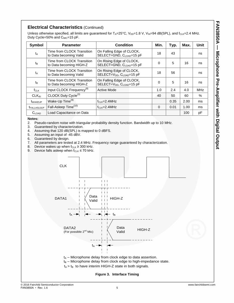
Electrical Characteristics (Continued)
Unless otherwise specified, all limits are guaranteed for TA=25°C, VDD=1.8 V, VIN=94 dB(SPL), and fCLK=2.4 MHz. Duty Cycle=50% and CMIC=15 pF.
Symbol Parameter Condition Min. Typ. Max. Unit
tA Time from CLOCK Transition to Data becoming Valid
On Falling Edge of CLOCK, SELECT=GND, CLOAD=15 pF
18 43 ns
tB Time from CLOCK Transition to Data becoming HIGH-Z
On Rising Edge of CLOCK, SELECT=GND, CLOAD=15 pF
0 5 16 ns
tA Time from CLOCK Transition to Data becoming Valid
On Rising Edge of CLOCK, SELECT=VDD, CLOAD=15 pF
18 56 ns
tB Time from CLOCK Transition to Data becoming HIGH-Z
On Falling Edge of CLOCK, SELECT=VDD, CLOAD=15 pF
0 5 16 ns
fCLK Input CLOCK Frequency(8)
Active Mode 1.0 2.4 4.0 MHz
CLKdc CLOCK Duty Cycle(3)
40 50 60 %
tWAKEUP Wake-Up Time(9)
fCLK=2.4MHz 0.35 2.00 ms
tFALLASLEEP Fall-Asleep Time(10)
fCLK=2.4MHz 0 0.01 1.00 ms
CLOAD Load Capacitance on Data 100 pF
Notes:
2. Pseudo-random noise with triangular probability density function. Bandwidth up to 10 MHz. 3. Guaranteed by characterization. 4. Assuming that 120 dB(SPL) is mapped to 0 dBFS. 5. Assuming an input of -45 dBV. 6. Guaranteed by design. 7. All parameters are tested at 2.4 MHz. Frequency range guaranteed by characterization. 8. Device wakes up when fCLK ≥ 300 kHz. 9. Device falls asleep when fCLK ≤ 70 kHz.
tA
tA
tB
CLK
DATA1 HIGH-ZData
Valid
DATA2(For possible 2
nd Mic)
HIGH-ZData
Valid
tA – Microphone delay from clock edge to data assertion.
tB – Microphone delay from clock edge to high-impedance state.
tA > tB to have interim HIGH-Z state in both signals.
Figure 3. Interface Timing
© 2016 Fairchild Semiconductor Corporation www.fairchildsemi.com FAN3850A • Rev. 1.6 6
FA
N3
85
0A
— M
icro
ph
on
e P
re-A
mp
lifier w
ith D
igita
l Ou
tpu
t
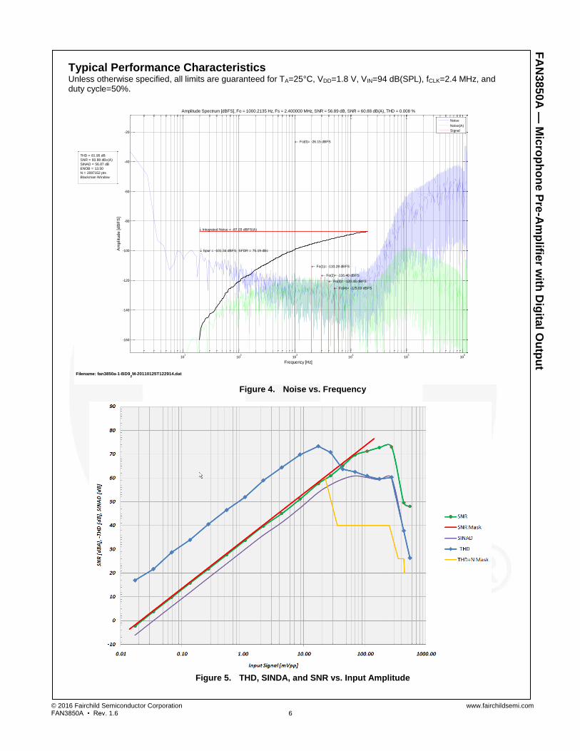
Typical Performance Characteristics Unless otherwise specified, all limits are guaranteed for TA=25°C, VDD=1.8 V, VIN=94 dB(SPL), fCLK=2.4 MHz, and duty cycle=50%.
Figure 4. Noise vs. Frequency
Figure 5. THD, SINDA, and SNR vs. Input Amplitude
101
102
103
104
105
106
-160
-140
-120
-100
-80
-60
-40
-20
Frequency [Hz]
Am
plitu
de
[d
BF
S]
Amplitude Spectrum [dBFS], Fo = 1000.2135 Hz, Fs = 2.400000 MHz, SNR = 56.89 dB, SNR = 60.88 dB(A), THD = 0.008 %
Fo(0)= -26.15 dBFS
Fo(1)= -110.28 dBFS
Fo(2)= -116.40 dBFS
Fo(3)= -120.45 dBFS
Fo(4)= -125.03 dBFS
Integrated Noise = -87.03 dBFS(A)
Spur = -101.34 dBFS, SFDR = 75.19 dBc
Noise
Noise(A)
Signal
Filename: fan3850a-1-BD92M-20110125T122914.dat
THD = 81.95 dB
SNR = 60.88 dBc(A)
SINAD = 56.87 dB
ENOB = 13.50
N = 2097152 pts
Blackman Window

© 2016 Fairchild Semiconductor Corporation www.fairchildsemi.com FAN3850A • Rev. 1.6 7
FA
N3
85
0A
— M
icro
ph
on
e P
re-A
mp
lifier w
ith D
igita
l Ou
tpu
t
Typical Performance Characteristics (Continued)
Figure 6. THD, SINAD, and SNR vs. Output Level
Figure 7. Δ Gain vs. Temperature (Nominal Temperature= 25°C)
Temp (˚C) Delta(dB)
-40 0.1971
-30 0.1644
-20 0.1260
-10 0.0954
0 0.0657
10 0.0359
20 0.0139
25 0.0000
30 -0.0097
40 -0.0344
50 -0.0514
60 -0.0739
70 -0.0998
80 -0.1183
85 -0.1271-40 -30 -20 -10 0 10 20 30 40 50 60 70 80
-4
-3
-2
-1
0
1
2
3
4
Junction Temperature -Tj ̊ C
ΔG
ain
(dB
)

© 2016 Fairchild Semiconductor Corporation www.fairchildsemi.com FAN3850A • Rev. 1.6 8
FA
N3
85
0A
— M
icro
ph
on
e P
re-A
mp
lifier w
ith D
igita
l Ou
tpu
t
Applications Information
Figure 8. Mono Microphone Application Circuit
Figure 9. Stereo Microphone Application Circuit
L/R
Decimation VDD
Interpolation
SELECT
SPEAKER
Applications Software
ADC
SELECT
CLK
Pre- Amp
SDI
ADC
INPUT
SDO
Pre- Amp
DATA
INPUT CLOCK
VDD
Serial Port
CLOCK
Audio Output
DATA
Low Pass Filter Noise Shaper
Decimation
Noise Shaper Low Pass Filter
INPUT
Serial Port CLK
Pre- Amp
Applications Software
ADC
Interpolation
CLOCK
SDI
DATA
SPEAKER VDD
SELECT SDO
Audio Output
L/R

© 2016 Fairchild Semiconductor Corporation www.fairchildsemi.com FAN3850A • Rev. 1.6 9
FA
N3
85
0A
— M
icro
ph
on
e P
re-A
mp
lifier w
ith D
igita
l Ou
tpu
t
Applications Information (Continued)
Diaphragm
Backplate
Airgap
Electret
FAN3850A
INPUT
CLOCK DATA SELECT
VDD
GND
Figure 10. MIC Element Drawing
A 0.1 µF decoupling capacitor is required for VDD. It can be located inside the microphone or on the PCB very close to the VDD pin.
Due to high input impedance, care should be taken to remove all flux used during the reflow soldering process.
A 100 Ω resistance is recommended on the clock output of the device driving the FAN3850A to minimize ringing and improve signal integrity.
For optimal PSR, route a trace to the VDD pin. Do not place a VDD plane under the device.
The table below pertains to the Marketing Outline drawing on the following page.
FAN3850A External Product Dimensions
Product ID D E X Y
All options 1.260mm 0.860mm 0.145mm 0.145mm

BOTTOM VIEW
TOP VIEW
1 2
A
B
C
6X
0.005 C A B
(X) +/-0.018
(Y) +/-0.018
Ø0.129±0.013
F
E
D
B
A
PIN A1
AREA
F
2X
2X
(Ø0.126)
CU PAD AT
BOTTOM
SIDE VIEWS
0.06 C
D
C
SEATING
PLANE
0.03 C
0.03 C
NOTES:
A. NO JEDEC REGISTRATION APPLIES.
B. DIMENSIONS ARE IN MILLIMETERS.
C. DIMENSIONS AND TOLERANCES PER
ASME Y14.5M, 2009.
D. DATUM C, THE SEATING PLANE IS DEFINED
BY THE SPHERICAL CROWNS OF THE BALLS.
E. PACKAGE TYPICAL HEIGHT IS 273 MICRONS
±23 MICRONS (254-300 MICRONS).
F. FOR DIMENSIONS D, E, X, AND Y SEE
PRODUCT DATASHEET.
G. DRAWING FILENAME: UC006AHrev4.
E
0.080±0.010
0.570
0.485
0.197±0.013
0.300
0.254
0.570
0.485
RECOMMENDED LAND
PATTERN (NSMD)
(Ø0.226)
SOLDER MASK
A1
0.01 C

www.onsemi.com1
ON Semiconductor and are trademarks of Semiconductor Components Industries, LLC dba ON Semiconductor or its subsidiaries in the United States and/or other countries.ON Semiconductor owns the rights to a number of patents, trademarks, copyrights, trade secrets, and other intellectual property. A listing of ON Semiconductor’s product/patentcoverage may be accessed at www.onsemi.com/site/pdf/Patent−Marking.pdf. ON Semiconductor reserves the right to make changes without further notice to any products herein.ON Semiconductor makes no warranty, representation or guarantee regarding the suitability of its products for any particular purpose, nor does ON Semiconductor assume any liabilityarising out of the application or use of any product or circuit, and specifically disclaims any and all liability, including without limitation special, consequential or incidental damages.Buyer is responsible for its products and applications using ON Semiconductor products, including compliance with all laws, regulations and safety requirements or standards,regardless of any support or applications information provided by ON Semiconductor. “Typical” parameters which may be provided in ON Semiconductor data sheets and/orspecifications can and do vary in different applications and actual performance may vary over time. All operating parameters, including “Typicals” must be validated for each customerapplication by customer’s technical experts. ON Semiconductor does not convey any license under its patent rights nor the rights of others. ON Semiconductor products are notdesigned, intended, or authorized for use as a critical component in life support systems or any FDA Class 3 medical devices or medical devices with a same or similar classificationin a foreign jurisdiction or any devices intended for implantation in the human body. Should Buyer purchase or use ON Semiconductor products for any such unintended or unauthorizedapplication, Buyer shall indemnify and hold ON Semiconductor and its officers, employees, subsidiaries, affiliates, and distributors harmless against all claims, costs, damages, andexpenses, and reasonable attorney fees arising out of, directly or indirectly, any claim of personal injury or death associated with such unintended or unauthorized use, even if suchclaim alleges that ON Semiconductor was negligent regarding the design or manufacture of the part. ON Semiconductor is an Equal Opportunity/Affirmative Action Employer. Thisliterature is subject to all applicable copyright laws and is not for resale in any manner.
PUBLICATION ORDERING INFORMATIONN. American Technical Support: 800−282−9855 Toll FreeUSA/Canada
Europe, Middle East and Africa Technical Support:Phone: 421 33 790 2910
Japan Customer Focus CenterPhone: 81−3−5817−1050
www.onsemi.com
LITERATURE FULFILLMENT:Literature Distribution Center for ON Semiconductor19521 E. 32nd Pkwy, Aurora, Colorado 80011 USAPhone: 303−675−2175 or 800−344−3860 Toll Free USA/CanadaFax: 303−675−2176 or 800−344−3867 Toll Free USA/CanadaEmail: [email protected]
ON Semiconductor Website: www.onsemi.com
Order Literature: http://www.onsemi.com/orderlit
For additional information, please contact your localSales Representative
© Semiconductor Components Industries, LLC