fabrication and characterization of as doped p-type …cdn.intechweb.org/pdfs/20515.pdf ·...
TRANSCRIPT

16
Fabrication and Characterization of As Doped p-Type ZnO Films Grown
by Magnetron Sputtering
J.C. Fan1,2, C.C. Ling2 and Z. Xie1,*
1College of Physics and Microelectronics Science, Key Laboratory for Micro-Nano Physics and Technology of Hunan Province, Hunan University,
2Department of Physics, The University of Hong Kong, People's Republic of China
1. Introduction
In the past decade, there has been a great deal of interest in zinc oxide ZnO semiconductor materials lately, as seen from a surge of a relevant number of publications in Figure 1 (Wenckstern, 2008). It can be seen that the present renaissance in ZnO research started in the mid 1990s. More than 2000 papers on ZnO were published in 2005 and even higher numbers in 2006.
Fig. 1. Publications per annum for the search of ZnO in the abstract before 2007, For 2007, only papers published before June 6th are considered. From Ref. (Wenckstern, 2008).
With a wide band gap of 3.4eV and a large exciton binding energy of 60 meV at room temperature, ZnO has been considered as a promising material for optoelectronic devices (Klingshirn, 2007): • ZnO as a blue/UV optoelectronics, including light emission diodes (LEDs) and laser
diodes in addition to (or instead of) the GaN –based structure.
www.intechopen.com

Optoelectronics - Materials and Techniques
394
• ZnO as a radiation-hard material for electronic devices in a corresponding environment. • ZnO as a material for electronic circuits, which is transparent in the visible. • ZnO as a diluted or ferromagnetic material, when doped with Co, Mn, Fe, V or similar
elements, for semiconductor spintronics. • ZnO as a transparent, highly conducting oxide (TCO), when doped with Al, Ga, In or
similar elements, as a cheaper alternative to indium tin oxide (ITO). More applications about ZnO can be found in references (Janotti & Van de Walle 2009). It is known that GaN is a III-V compound semiconductor material with in the hexagonal wurtzite-type structure and an important application in optoelectronic devices. With a similar crystallinity to GaN, ZnO has more advantages in optoelectronic application (Özgϋr, et al., 2005; Shur & Davis, 2004; Tsukazak, et al., 2005; Look, 2001; Janotti & Van de Walle 2009): • a exciton binding energy of 60 meV at room temperature(RT) is higher than one of GaN
(24meV), resulting in ZnO can be excited at RT and prepared the optoelectronic devices in shorter wavelength.
• the band gap of ZnO (Eg =3.4 eV) can be effectively modulated (controled) in 3- 4.5eV by doping Cd or Mg.
• ZnO film can be fabricated with large area and good uniformity on various substrates, leading to the application in a wider field, however, GaN film is prepared on some limited substrates (SiC, Sapphire, Si).
• the growth temperature for high quality ZnO film is about 5000C, which is much lower than that for GaN film (≥10000C).
The properties of GaN and ZnO are summarized in Table1 (Madelung, 1996; Norton et al, 2004).
Table 1. The properties of GaN and ZnO. From Ref. (Madelung, 1996; Norton, et al, 2004).
www.intechopen.com

Fabrication and Characterization of As Doped p-Type ZnO Films Grown by Magnetron Sputtering
395
Fig. 2. (a) The structure of a typical p–i–n junction LED. (b) Current–voltage characteristics of a p–i–n junction. The inset has logarithmic scale in current with F and R denoting forward and reverse bias conditions, respectively. (c) Electroluminescence spectrum from the p–i–n junction (blue) and photoluminescence (PL) spectrum of a p-type ZnO film measured at 300K. From Ref. (Tsukazak, et al., 2005 ).
www.intechopen.com

Optoelectronics - Materials and Techniques
396
Figure 2a shows the schematic structure of a typical homostructural p–i–n junction prepared by Tsukaza et al. The I-V curve of the device displayed the good rectification with a threshold voltage of about 7V (Figure 1b). The electroluminescence spectrum from the p–i–n junction (blue) and photoluminescence (PL) spectrum of a p-type ZnO film at 300K were shown in Figure 1c, which indicated that ZnO was a potential material for making short-wavelength optoelectronic devices, such as LEDs for display, solid-state illumination and photodetector.
2. ZnO basic properties
ZnO is a II-V semiconductor with the ionicity at the borderline between covalent and ionic semiconductor (Özgϋr, et al., 2005). ZnO has three crystal structures: rocksalt, zinc blende and wurtzite, as shown in Figure 3(a), (b) and (c), respectively. Under conventional conditions, the thermodynamically stable phase is wurtzite, which has a hexagonal unit cell with space group C6v 4or p63mc, and lattice parameters a = 0.3296, and c = 0.52065 nm. In this structure, the oxygen anions (O2-) and Zn cations (Zn2+) form a tetrahedral unit, composing two interpenetrating hexagonal-close-packed (hcp) sublattices and each sublattice includes four atoms per unit cell and every atom of one kind(group-II atom) is surrounded by four atoms of the other kind (groupVI), or vice versa, as shown in Figure 3(c). The wurtzite structure of ZnO lacks central symmetry and can be simply considered a number of alternating planes composed of O2- and Zn2+, grown alternatively along the c-axis due to the low formation energy of the direction. The zinc-blende ZnO structure can be stabilized only by growth on cubic substrates, and the rocksalt (NaCl) structure may be fabricated at relatively high pressures. The wurtzite ZnO can be transformed to the rocksalt structure at relatively modest external hydrostatic pressures. In addition to the above crystal structures, theoretical calculation showed that a fourth phase of ZnO, cubic cesium chloride, may be possible at extremely high temperatures, however, the result has not been proved, experimentally.
(a) (b) (c)
Fig. 3. ZnO crystal structures: (a) rocksalt, (b) zinc blende, (c) wurtzite. The shaded gray and black spheres denote Zn and O atoms, respectively. From Ref.(Özgϋr, et al., 2005).
Other basic properties of ZnO can be seen from Table 1. Figures 4, 5 and 6 show the morphologies of ZnO single crystal, powder, film and nanomaterials.
www.intechopen.com

Fabrication and Characterization of As Doped p-Type ZnO Films Grown by Magnetron Sputtering
397
(a) (b) (c)
Fig. 4. Photographs of large bulk ZnO single crystals grown by different techniques: (a) gas transport, (b) hydrothermal, and (c) pressurized melt growth. From Ref.(Janotti, et al., 2009; Klingshirn, 2007).
Fig. 5. SEM images of the ZnO powder (a) and ZnO film(b).
Fig. 6. A collection nanostructures of ZnO. From Ref. (Wang, 2004; Yu et al.,2005).
3. Challenges in ZnO
ZnO has a strong potential for various short-wavelength optoelectronic device applications. However, to realize these applications, a reliable technique for fabricating high quality p-type ZnO and p-n junction needs to be established. Compared with other II-VI semiconductor and GaN, it is a major challenge to dope ZnO to produce p-type
www.intechopen.com

Optoelectronics - Materials and Techniques
398
semiconductor due to self-compensation from native donor defects and/or hydrogen incorporation(Wang, et al., 2004; Xiu, et al., 2005). Great efforts have been made to achieve p-type ZnO by mono-doping group-I elements(Li, Na and K), group-IB elements(Ag and Cu) or group-V elements (N, P, As, and Sb) and co-doping III–V elements with various technologies, such as evaporation/sputtering process, ion implantation, pulsed laser deposition, thermal diffusion of As after depositing a ZnO film on GaAs substrate, and hybrid beam deposition(McCluskey & Jokela, 2009; Yan, et al., 2006; Kang, et al., 2006; Özgϋr, et al., 2005; Look, et al., 2004; Marfaing & Lusson, 2005; Yan&Zhang, 2001; Yamamoto, 2002). It is believed that the most promising dopants for p-type ZnO are the group V elements, although theory suggests some difficulty in achieving shallow acceptor level. The first p-type ZnO with a hole concentration of 1016–1017 cm–3 was reported in films made by vapour-phase transport in NH3, followed by molecular beam epitaxy (MBE) with an atomic nitrogen source (Minegishi, et al., 1997). The mechanism of p-type ZnO:N is considered that N substitutes for an O, forming an acceptor with a hole binding energy of 400meV according to first-principles calculations(Park, et al., 2002), and x-ray absorption spectroscopy verified that N occupies the O substitutional site in Fons’s experiment, which is consistent with the radius of N is near with that of O (Fons et al., 2006). P, As and Sb in ZnO are deep acceptor because of their large ionic radii as compared to O. However, some researchers claimed that p-type ZnO were achieved with these large-size-mismatched impurities (Heo, et al., 2003; Ryu, et al., 2000; Xiu, et al., 2005). Therefore, the microscopic structure of these impurities in ZnO has not been understood completely, which can not been contributed to these impurities occupied O site to generate holes, simply. In this paper, we fabricated p type As doped ZnO films on glass and SiO2/Si substrates at different temperature by sputtering Zn3As2/ZnO target or cosputtering Zn3As2 and ZnO targets, and investigated the optical and electrical properties of the films, systematically. Especially, the mechanism of p-type conductivity of ZnO: As film was discussed according to AsZn–2VZn shallow acceptor model proposed by Limpijumnong et al., which helped to understand the microscopic structure of As in As-doped ZnO and the microscopic origin of p-type ZnO by doping large-size- mismatched impurities.
4. Experiment
Magnetron sputtering (DC sputtering, RF magnetron sputtering, and reactive sputtering) is one of the popular growth techniques for ZnO investigations because of its low cost, simplicity and low operating temperature. A schematic diagram of the magnetron sputtering system in our experiments is shown in Figure 7. Figure 8 shows a photograph of the typical glow from ZnO target when sputtering. As-doped ZnO films were grown on glass and SiO2/Si substrates at different substrate temperatures by sputtering Zn3As2/ZnO or cosputtering ZnO and Zn3As2 targets. Undoped ZnO films were deposited by sputtering ZnO target. Silicon oxide layer with a thickness of 250 nm was thermally grown in dry oxygen on Si substrate. The substrates were first cleaned by acetone and ethanol and then rinsed in de-ionized water each for 5 min at room temperature. The sputtering chamber was evacuated to a base pressure of 10-3Pa. A pure Ar (99.999%) was used as the working gas. The distance between the targets and the substrate was 14cm. The targets were presputtered for 20 min to remove contaminants. The As-doped ZnO targets were prepared by adding Zn3As2 and sintering at 9000C for 3h. The Zn3As2 contents in the targets were 0.5mol%, 1.0mol%,1.5mol%,2mol%, respectively. The pure Zn3As2 target was sintered in pure Ar (purity: 99.999%; pressure: 0.1MPa) at 8000C for 2h. The film thickness was measured with ellipsometer.
www.intechopen.com

Fabrication and Characterization of As Doped p-Type ZnO Films Grown by Magnetron Sputtering
399
Fig. 7. Schematic diagram of the magnetron sputtering system.
Fig. 8. Photograph of the typical glow from ZnO target when sputtering.
The structures and morphologies of the as-grown ZnO films were characterized by X-ray diffraction (XRD, Siemens D-5000, and Cu Ka, λ = 1.5405Å), atomic force microscopy (AFM, NTD-Pro47) and scan electron microscopy (SEM, JSM-6700F). The composition of As-doped ZnO film was analyzed by an energy dispersive X-ray (EDX) spectroscopy (INCA, Oxford) attached to the SEM. The concentration of As in ZnO film was measured with Secondary ion mass spectroscopy (SIMS, Physical Electronicsmodel 7200). The bonding state of As in ZnO:As films were studied by x-ray photoelectron spectroscopy (XPS) using the Mg Kα line (Physical Electronics model5600). The x-ray source and the C 1s line were taken as the standard reference. The electrical properties of the films were investigated at room temperature in the Van der Pauw configuration using HL5500 Hall system. The measurement process was the following: ensuring Ohmic contact→the resistivity measurement→Hall effect measurement→repeating Hall effect measurement. During the whole measurement, the resistivity was measured once and every sample had one value of the resistivity and several values of the mobility and carrier concentration. For one sample, if the results of several Hall effect measurements showed the same
www.intechopen.com

Optoelectronics - Materials and Techniques
400
conduction type, we consider it had stable conduction type. If the results of several Hall effect measurements were not consistent, and the conduction type of the film was not confirmed. The optical transmission spectra of the films were measured at room temperature using an UV–vis double beam spectrometer. Low temperature photoluminescence (PL) were systematically performed for ZnO films by the excitation from 325 nm He-Cd laser.
5. Results and discussion
5.1 Undoped ZnO films First, let us investigate the properties of undoped ZnO films grown by magnetron sputtering. The undoped ZnO films were deposited on glass substrates at various temperatures from 250 to 4500C with RF power of 120W. High purity Ar (99.999%) or mixture of Ar and O2 (Ar:O2 = 3:1) maintained at 0.6 Pa was used as the working gas. In addition, the ZnO film measured low temperature PL was prepared on SiO2/Si substrate at 3500C with purity Ar maintained at 0.5 Pa. Figure 9 shows the XRD patterns of ZnO powder and film deposited at 4500C.
Fig. 9. XRD patterns of ZnO powder (a) and film deposited at 4500C (b).
Many diffraction peaks, such as (100), (002), (101) were seen in the pattern of ZnO powder and the (002) peak was not the strongest one. In the pattern of ZnO film deposited at 4500C, a strong peak of (002) at about 34.50 and a weak peak of (004) at 72.60 were observed. Comparison of the patterns shows that the thin film tended to be oriented on the (001) surface. SEM photograph in Figure 5 showed that the grains of ZnO film were small, around 100nm in diameter, in which exhibited hexagonal form and the powder were composed of ZnO grains with different diameters. The optical absorption spectra of ZnO powder and film deposited at 4500C in the visible are displayed in Figure 10. The fundamental absorption for both powder and film starts from about 370 nm and the absorption of film in UV region was stronger, obviously. The inset shows a plot of (αhν)2 against hν for ZnO film and the optical band gap (Eg) value was obtained by extrapolating the linear portion to photo energy axis. It was found to be about 3.262eV.
www.intechopen.com

Fabrication and Characterization of As Doped p-Type ZnO Films Grown by Magnetron Sputtering
401
Fig. 10. Absorption spectra of ZnO powder (b) and film (a).The film thickness was about 300 nm. Inset shows plot of (ahv)2 against hv for estimation of direct allowed optical gap of the film. The estimated gap was 3.262eV.
Figure 11 shows XRD patterns of ZnO films grown with different conditions. The growth parameters of the films were summarized in Table 2. A strong peak of ZnO (002) at about 34.50 was observed for each sample, indicating that the films were c-axis oriented. The full-width at half-maximum (FWHM) of (002) peaks were listed in Table 2. (103) peak in the XRD pattern of the film grown at 2500C (SampleSA) shows that c-axis oriented grains in the film did mot dominate completely due to the low growth temperature. (103) peak disappeared in the films deposited at 3500C (SampleSB), indicating the c-axis orientation of the film became stronger and the crystallinity was improved, which was consist with the change of (002) FWHM from 0.400 to 0.380. Comparison of the patterns of SamleSB, SC and SB+annealing shows that the induction of O2 in working gas and post-annealed improved the quality of ZnO films grown with magnetron sputtering.
Fig. 11. XRD patterns of ZnO films grown different conditions: (a) PAr =0.6Pa, 2500C; (b) PAr
=0.6Pa, 3500C; (c) PAr =0.45Pa, PO2 =0.15Pa, 3500C.
www.intechopen.com

Optoelectronics - Materials and Techniques
402
Table 2. Growth parameters and (002) FWHM of ZnO films.
Fig. 12. XRD patterns of as-grown ZnO film at 3500C and annealed at 450 0C in air for 2h.
The surface morphologies of ZnO films were investigated by AFM. Figure 13 shows AFM images of ZnO films grown with different conditions. It can be seen that the grains of the films became larger with the temperature increased from 250 to 3500C and post-annealing improved the uniform of the film, which indicated the crystallinity of the films improved and were consisted with the results of XRD. Figure 14 shows the optical transmittance spectra of ZnO films. The transmittances are over 70% in the visible region for all the films and the fundamental absorptions are at about 370nm. The inset of Figure 14 reveals the relationship between absorption coefficient and photo energy of ZnO film deposited at 3500C. The Eg value estimated was 3.271 eV. Low temperature PL was performed for ZnO film grown on SiO2/Si substrate. The near band edge (NBE) part of the 10 K PL spectrum was shown in Figure 15, which had peaks at 3.355, 3.308, and 3.234eV (Fan, et al., 2009). Similar lines were also observed by Petersen et al., (3.350 and 3.303eV) in n-type ZnO grown by sol-gel process (Petersen, et al., 2008 )and by Zhong et al (3.357 and 3.309eV) in ZnO tetrapod(Zhong, et al., 2008). The ~3.36 eV was ascribed to the neutral donor-bound-exciton (D0X) according to D.C.Look 's suggestion about the peak (Look & Clalin,2004). The 3.31 eV line was associated with the corresponding two-electron-satellite (TES) and/or exciton-LO phonon emission, therefore, the peaks at 3.355 and 3.308eV in Figure 15 were assigned to be the D0X and the TES/exciton-LO phonon lines, respectively. The 3.234 eV observed in Figure 15 was similar to the ~3.24eV donor-acceptor-pair (DAP) emission suggested by Peterson et al (Petersen, et al., 2008), and were thus assigned as DAP.
www.intechopen.com

Fabrication and Characterization of As Doped p-Type ZnO Films Grown by Magnetron Sputtering
403
(a) (b)
(c)
Fig. 13. AFM images of ZnO films prepared with different conditions:(a) PAr =0.6Pa, 2500C; (b) PAr =0.6Pa, 3500C; (c) SB+annealing.
Fig. 14. Transmittance spectra of as-grown ZnO films prepared with different conditions: (a) PAr =0.6Pa, Room temperature; (b) PAr =0.6Pa, 2500C; (c)PAr =0.6Pa, 3500C; The inset is the (αhν)2 vs hν curve for the optical band gap determination in the filmdeposited at 3500C. The Eg value estimated was 3.271eV.
www.intechopen.com

Optoelectronics - Materials and Techniques
404
Fig. 15. NBE region of 10 K PL spectra for ZnO film grown on SiO2/Si substrate at 3500C.
5.2 As doped ZnO films prepared by sputtering Zn3As2/ZnO target As doped ZnO films were prepared on glass and SiO2/Si substrates by sputtering Zn3As2/ZnO target at a substrate temperature from 50 to 4500C, respectively. The Zn3As2 contents in the targets were 0.5mol%, 1.0mol%, 1.5mol%, respectively. A pure Ar (99.999%) at 0.6 Pa was used as the working gas. The films were deposited with a radio frequency (RF) power from 80 to 150W, respectively. The total thickness of the films was about 300 nm. In addition, the As-doped ZnO fims performed low temperature PL were prepared on SiO2/Si substrates at 250 and 3500C with purity Ar maintained at 0.5 Pa, using the target with 1mol% Zn3As2 and ZnO target. Figure 16 shows the XRD patterns of As-doped ZnO films deposited on glass substrates at different temperatures. A strong peak of (0 0 2) at about 34.50 for all samples was observed, indicating that the films were c-axis oriented. Two peaks corresponding to (1 1 0) and (1 1 1) of Zn3As2 , respectively, were detected in the patterns of the films deposited at 50 and 2500C, indicating the films were ZnO/Zn3As2 or ZnO:As/Zn3As2 ones (samplesA and B). However, no diffraction peaks associated with Zn3As2 were detected in the patterns of ZnO films deposited at 350 and 4500C, revealing the films were ZnO:As ones, corresponding to samples C and D, respectively.
Fig. 16. XRD patterns of As-doped ZnO films deposited on glass substrates at different temperatures: 500C (a); 2500C (b); 3500C (c); 4500C (d). From Ref.(Fan, et al., 2007a).
www.intechopen.com

Fabrication and Characterization of As Doped p-Type ZnO Films Grown by Magnetron Sputtering
405
Similar phenomenon was observed in the XRD spectra of As-doped ZnO films deposited SiO2/Si substrates with different conditions, as shown in Figure 17, and the growth parameters were summarized in Table 3. The (110) and (111) peaks of Zn3As2 were detected in the patterns of Samples S1, S2, S4 and S7, which showed that the films were ZnO/Zn3As2 or ZnO:As/Zn3As2 ones. Only ZnO (002) peak was observed in the patterns of Samples S3, S5 and S6, indicating the films were ZnO:As ones. Therefore, the growth parameters of ZnO:As film in our experiments were summarized in Table 4.
Table 3. Growth parameters of As-doped ZnO films on SiO2/Si substrates.
Fig. 17. (a) XRD patterns As-doped ZnO films deposited at 3500C with various RF powers from 100 to 150W(samples S1, S2, and S3). (b) XRD patterns As-doped ZnO films deposited with RF powers of 120W at 300–4000C (samples S2, S4, and S5). (c) XRD patterns As-doped ZnO films deposited with RF powers of 120W at 3500C by sputtering 0.5-1.5mol% Zn3As2/ ZnO targets (samples S5, S6, and S7).
www.intechopen.com

Optoelectronics - Materials and Techniques
406
Table 4. Growth parameters of ZnO:As films in our experiments
The surface morphology of ZnO:As films in our experiments were investigated by AFM and SEM. Figure 18 shows AFM images of ZnO:As film deposited on glass at 3500C (SampleC). It can be seen that the film was composed of globe-like grains and had high quality, which was consist with XRD results in Figure 16.
Fig. 18. AFM images of ZnO:As film deposited on glass at 3500C (SampleC).
The microstructure of the ZnO:As films grown on SiO2/Si substrates was characterized using SEM. The SEM micrographs of the films revealed that the films had a homogeneous surface formed by globe-like grains, indicating high quality of the film microstructure. The typical SEM images obtained for samples S3 and S5 are shown in Figure 19.
(a) (b)
Fig. 19. SEM images of ZnO:As film deposited on SiO2/Si substrates: (a), Sample S3; (b), Sample S5.
www.intechopen.com

Fabrication and Characterization of As Doped p-Type ZnO Films Grown by Magnetron Sputtering
407
EDS and SIMS analyses were carried out to study the As-doping content in ZnO:As films. EDS was performed in two different areas of the samples to confirm whether the films contain As or not. Figure 20 shows the typical EDS spectrum of ZnO:As film deposited at 3500C on glass, which indicated that the presence of element As besides Zn, O, Ca and Si. Obviously, the peaks of Ca and Si should be ascribed to the glass substrate. The element content in the film is illustrated in Table5 (Fan, et al., 2007a). It can be seen that the film contained almost the same As content in its different areas.
Fig. 20. EDS spectrum of ZnO:As film grown at 3500C on glass.
Table 5. Content (at%) analysis of various elements in the ZnO:As film deposited at 3500C using EDS. From Ref. (Fan, et al., 2007a).
Fig. 21. SIMS spectrum showing the As depth profile of the As-doped ZnO film grown at 450oC on SiO2/Si substrate.
SIMS was characterized for ZnO:As films deposited on SiO2/Si substrate at 4500C with Ar at 0.5 Pa as working gas, as exhibited in Figure 21. The As element was found to be uniformly distributed in the film sample down to a depth of ~280nm.
www.intechopen.com

Optoelectronics - Materials and Techniques
408
XPS was employed to investigate the chemical states of As atoms in ZnO:As films. Figure 22 shows the typical XPS spectra of the As3d, Zn2p and O1s core-level spectra for ZnO:As film. The As (3d) binding energies of the As-O and As-Zn bonds were associated with the values of ~45 eV and 41eV, respectively. The observation of the 44.8eV single peak in the As (3d) binding energy in XPS spectrum of ZnO:As film implied that the As atoms occupied the Zn site of the ZnO lattice, which was consistent with the results obtained by Wahl (Wahl, et al., 2005). Asymmetric O1s peak was detected for the sample, which had a shoulder at the higher binding energy side fitting with Gaussian distribution. The buildup of two peaks at 530.53 and 531.93eV was observed. The domination peak at 530.53 was attributed to the O2−
ion in the wurtzite structure surrounded by the Zn ions. The peak at 531.93eV was assigned to loosely bound oxygen, such as absorbed O2 or adsorbed H2O on the ZnO surface or H- implanted in the fabrication of ZnO:As film, which was consistent with the result of SIMS. Two peaks at 1021.73eV and 1044.83eV with a spin-orbit splitting of 23.1eV, corresponding to Zn2p3/2 and Zn2p1/2, respectively were seen in Zn2p XPS spectrum, which coincided with the findings for the Zn2+ bound to oxygen in the ZnO Matrix.
Fig. 22. (a) As3d, (b) Zn2p and (c) O1s core-level spectra for ZnO:As film.
Hall effect measurements were performed on As-doped ZnO films on glass and SiO2/Si substrates at room temperature. The electrical properties of As-doped ZnO films on glass substrates are summarized in Tables 6 (Fan, et al., 2007a) and 7.
www.intechopen.com

Fabrication and Characterization of As Doped p-Type ZnO Films Grown by Magnetron Sputtering
409
Table 6. Electrical properties of As-doped ZnO films on glass at different substrate temperatures with RF power of 120W. From Ref.(Fan, et al., 2007a).
Table 7. Electrical properties of As-doped ZnO films on glass with various RF powers at 3500C.
From Tables 6 and 7, it can be seen that the As-doped ZnO films fabricated with various conditions exhibited different conduction types. The film grown at 500C (SampleA) was n type with a carrier concentration of 3.46×1018cm-3, a mobility of 0.979cm2/Vs, a resistivity of 1.84Ωcm, however, Sample B, deposited at 2500C, became p-type (p = 8.99×1017cm-3, μh = 0.891 cm2/Vs, R= 7.8Ωcm ), Sample C grown at 3500C, showed p type, exhibiting a 6.88×1017cm-3 carrier concentration, a 0.3 cm2/Vs mobility and 30.3Ωcm resistivity. While the substrate temperature was increased to 4500C or rf power became 150W from 120W at 3500C, corresponding to Sample D (n = 3.51×1016cm--3, μe = 1.96cm2/Vs, R= 90.7Ωcm ) and sample E (n = 1.39×1017cm-3, μe = 0.935 cm2/Vs, R= 48.2Ωcm ), respectively, the samples exhibited n type. For the mechanism of p-type conductivity of ZnO by doping large-size-match impurites, such as P, As and Sb, Limpijumnong et al proposed AsZn–2VZn acceptor Model (Limpijumnong, et al., 2005; Fan, et al., 2007a). This doping mechanism differs from the substitution mechanism of As into O site (AsO), in which As atom occupies Zn antisite, not O sites, forming AsZn–2VZn acceptor with the ionization energy of 0.15eV. The process can be written as:
( )3 2Zn Zn Zn ZnAs V As V ++ −
− → − (1)
( ) ( )2Zn Zn Zn Zn ZnAs V V As 2V+ −−
− + → − (2)
The formation energy of AsZn–2VZn is lower than that of AsZn and AsZn–VZn and its formation is easier, comparatively. Both AsZn and AsZn–VZn are donors and AsZn–2VZn is acceptor. Zn3As2 is a p-type semiconductor materials. Obviously, the p-type conductivity of the As-doped films deposited for this study can be attributed to Zn3As2 and/or AsZn–2VZn
complex, while the n-type conductivity is due to AsZn, AsZn–VZn, intrinsic donor defects (Vo and Zni) and hydrogen as an unintentional extrinsic donor in ZnO films. For Sample A,
www.intechopen.com

Optoelectronics - Materials and Techniques
410
grown at 500C, the electron concentration associated with donor defects (AsZn, AsZn–VZn, Vo, Zni and H ) was higher than the hole concentration related to Zn3As2 and AsZn–2VZn complex, and for sample B, deposited at 2500C, was lower, therefore, sampleA showed n-type conduction and sample B was p-type. For sample C, ZnO:As films deposited at 3500C, only AsZn–2VZn complex acted as acceptor in the film, therefore, hole in the film decreased when substrate temperature increased from 250 to 3500C, however, it was majority carrier. The n-type conductivity of samplesD and E was mostly due to form plentiful AsZn and AsZn–VZn, resulting in electron became majority carrier. In attempting to further understand the thermal induced n-to-p-type conversion of the ZnO:As films, we have carried out Ar-atmosphere annealing study on the n-type ZnO:As film grown on the glass substrate at 4500C. After 4000C annealing for 60min, the film was converted from n type to p type having p = 9.10×1015 cm-3, as shown in table 8.
Table 8. Electrical properties of ZnO:As film (SampleD) post-annealing. From Ref.(Fan, et al., 2007a).
Similar changes of the conduction type were also found for As-doping ZnO films fabricated on SiO2/Si substrates with various conditions, as summarized in table 9, which was agreement with the AsZn–2VZn acceptor Model (Fan & Xie, 2008b).
Table 9. Growth parameters and electrical properties of As-doped ZnO films fabricated on SiO2/Si substrates. From Ref.(Fan&Xie, 2008b).
Figure 23 shows the optical transmittance spectra of undoped ZnO and ZnO:As films deposited on glass at 3500C. The transmittances were over 70% in the visible region and the fundamental absorption edges were clearly observed the films. Compared the absorption edges of the films, the absorption edge of ZnO:As film shifted to short-wavelength, the phenomenon can be observed in the inset of Figure 23, which reveals the relationship between absorption coefficient and photo energy. The optical band gap (Eg) value was obtained by extrapolating the linear portion to photo energy axis. As shown in the inset of Figure 23, the Eg values of the films blueshifted from 3.271 to 3.325eV.
www.intechopen.com

Fabrication and Characterization of As Doped p-Type ZnO Films Grown by Magnetron Sputtering
411
Fig. 23. Transmittance spectra of undoped ZnO (a) and ZnO:As (b) films deposited on glass at 3500C. The inset is the (ahν)2 vs hν curves for the optical band gap determination in the films.
Figure 24 shows the NBE PL spectrum at 10K of the p-type ZnO:As film deposited on SiO2/Si substrate. This film shows the dominant A0X at 3.337eV and small emission lines such as the free electron to acceptor recombination (FA) at 3.282 eV and the donor acceptor pair emissions at 3.236, 3.197 and 3.158eV (Fan, et al., 2009; Fan, et al., 2010). The acceptor binding energy (ionization energy) can be calculated by equation (1)
A gap FA BE E E k T / 2,= − + (1)
where Egap =3.437eV and EFA =3.282eV were the band gap energy and the temperature dependent transition energy, respectively. The value of EA was calculated to be 155meV, which was nearly consistent with the ionization energy of AsZn–2VZn as a shallow acceptor in ZnO (=0.15 eV). That is the As substitutes on the Zn site, then it induces two Zn-vacancy acceptors, forming AsZn–2VZn acceptor, which is good agreement with the result about the A3d XPS spectrum.
Fig. 24. NBE region of 10 K PL spectrum for p-type ZnO:As film deposited on SiO2/Si substrate.
www.intechopen.com

Optoelectronics - Materials and Techniques
412
5.3 As doped ZnO films prepared by co-sputtering Zn3As2 and ZnO targets As-doped ZnO films were deposited on glass substrates by co-sputtering two targets: a pure ZnO and a pure Zn3As2. The working argon pressure was kept at 1.0Pa, and the substrate temperature was in the range of 250 to 5000C. The films were deposited with the RF power of 100W on ZnO target and various direct current (DC)powers (0, 2.5, 7.6 and 9.7W) on Zn3As2 target. The grown parameters of the films were summarized in Table10. After deposition, post-annealing was carried out for SampleG at 350 and 4500C, respectively, in Ar ambient for 30min. The thickness of the films was in the range of 100 to 200nm.
Table 10. The grown parameters of As-doped ZnO by co-sputtering.
Fig. 25. XRD patterns of As-doped ZnO films with different DC powers on Zn3As2 target: (F) 0W, (G) 7.6 W, and (H) 9.7 W. From Ref.(Fan, et al., 2007b).
XRD spectra of the As-doped ZnO films grown with various DC powers on Zn3As2 target had a dominate peak at about 34.40 corresponding to the ZnO (002), and no peaks about Zn3As2, as shown in Figure 25, which indicated the films had single phase wurtzite structure and the c-axis preferred orientation. The appearance of ZnO(101) peak for sample H showed that the crystallinity of the film degredated due to mass As doping, observably. Figure 26 showed the XRD patterns of As-doped ZnO films deposited at different temperatures. The peak of Zn3As2 (111) in the XRD pattern of the film deposited at 2500C indicated that the film was ZnO/Zn3As2 or ZnO:As/Zn3As2 one. For the samples fabricated at T >2500C, only ZnO
www.intechopen.com

Fabrication and Characterization of As Doped p-Type ZnO Films Grown by Magnetron Sputtering
413
peaks such as (100), (002), (101), (103) and (004), were observed, indicating that the films were ZnO:As ones. Obviously, the crystallinity of the films improved when the temperature increased from 250 to 4000C, and then became poor when T>4000C.This can be interpreted from nucleation theory.
Fig. 26. XRD patterns of As-doped ZnO films grown at various temperatures: 2500C(I), 3000C (J), 350 0C(K), 4000C (L), 450 0C (M), and 500 0C(N). From Ref.(Fan&Xie, 2008a).
The typical XRD patterns of as-grown and annealed ZnO:As films were shown in Figure 27. It can be seen that the ZnO:As films remained the c-axis preferred orientation and the crystallinity did not change observably with annealing treatment in our experiment.
Fig. 27. XRD patterns of the as-grown SampleG and annealed ZnO:As films with different annealing temperatures.
The surface morphology of As-doped ZnO films by co-sputtering were analysized using SEM. Figure 28 showed the SEM micrographs of ZnO:As film(SampleG: DC power of 7.6W on Zn3As2 target) and SampleG+annealing at 4500C. The film had a homogeneous surface formed by nano-grains and post-annealing in our experiment did not change the quality of the film, observably, which was consistent with the XRD result (Figure 27).
www.intechopen.com

Optoelectronics - Materials and Techniques
414
Fig. 28. The SEM micrographs of ZnO:As film(SampleG)(a) and SampleG+annealing at 4500C(b).
Fig. 29. The SEM micrographs of ZnO:As films deposited at various temperatures: 3500C(a), 4000C(b), (c)4500C, (d) the higher resolution of Fig.29.b .
The SEM micrographs of ZnO:As films deposited with DC power of 2.5W on Zn3As2 target at substrate temperatures from350 to 4500C, corresponding to SamplesK, L and M, respectively. It can been that the ZnO:As films with c-axis preferred orientation had
www.intechopen.com

Fabrication and Characterization of As Doped p-Type ZnO Films Grown by Magnetron Sputtering
415
homogeneous surface formed by globle-like grains, indicating the high quality of the films, the nonuniform surface of Sample M grown at 4500C was attributed that excessive As atoms in ZnO structure lead to poor crystallinity at higher temperature. It was noted that the grains like ones in the film deposited at 4500C (Figure 29c) was detected in the film deposited at 4000C, as shown in Figure 29d. XPS analysis was performed for ZnO:As films deposited by co-sputtering to investigate bonding state of As in the films. The typical XPS patterns were shown in Figure 30. Only a peak at 44.8eV was detected in As3d XPS spectrum, corresponding to As–O, indicating that As was in its oxidization state and it replaced Zn site in the ZnO:As film. A dominated symmetric O 1s peak at 531.2eV was observed, as shown in Figure 30b, indicating the O2−
ion in the wurtzite structure surrounded by the Zn ions. Figure 30c shows two peaks at 1021.7 and 1044.9eV, corresponding to Zn2p3/2 and Zn2p1/2, respectively. The results about As and Zn chemical bonding were similar to the ones obtained for p-type ZnO:As film gown by sputtering Zn3As2/ZnO target.
Fig. 30. The typical (a) As3d, (b) Zn2p and (c) O1s core-level spectra for ZnO:As film grown by co-sputtering (SampleH).
The electrical properties of As-doped ZnO films grown with different conditions were characterized by Hall effect measurements at room temperature. The results were summarized in Tables11 and 12. It noted that the as-grown ZnO:As films deposited with various conditions exhibited different conduction types. For Sample G, deposited at 3500C with DC power of 7.6W on Zn3As2 target showed n type conductivity: n = 1.33×1018cm-3, μe = 0.215cm2/Vs, R= 21.8Ωcm, however, SampleH, grown at 3500C with DC power of 9.7W on Zn3As2 target, exhibited p type behavior with a carrier concentration of 8.42×1016 cm-3, a
www.intechopen.com
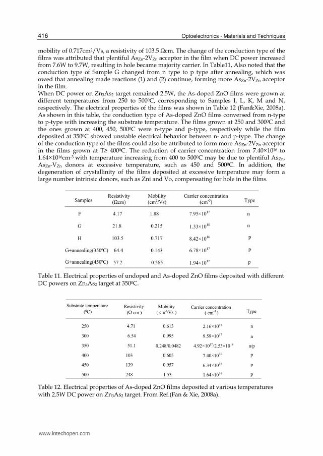
Optoelectronics - Materials and Techniques
416
mobility of 0.717cm2/Vs, a resistivity of 103.5 Ωcm. The change of the conduction type of the films was attributed that plentiful AsZn-2VZn acceptor in the film when DC power increased from 7.6W to 9.7W, resulting in hole became majority carrier. In Table11, Also noted that the conduction type of Sample G changed from n type to p type after annealing, which was owed that annealing made reactions (1) and (2) continue, forming more AsZn-2VZn acceptor in the film. When DC power on Zn3As2 target remained 2.5W, the As-doped ZnO films were grown at different temperatures from 250 to 5000C, corresponding to Samples I, L, K, M and N, respectively. The electrical properties of the films was shown in Table 12 (Fan&Xie, 2008a). As shown in this table, the conduction type of As-doped ZnO films conversed from n-type to p-type with increasing the substrate temperature. The films grown at 250 and 3000C and the ones grown at 400, 450, 5000C were n-type and p-type, respectively while the film deposited at 3500C showed unstable electrical behavior between n- and p-type. The change of the conduction type of the films could also be attributed to form more AsZn-2VZn acceptor in the films grown at T≥ 4000C. The reduction of carrier concentration from 7.40×10¹⁶ to 1.64×1016cm-3 with temperature increasing from 400 to 5000C may be due to plentiful AsZn, AsZn-VZn donors at excessive temperature, such as 450 and 5000C. In addition, the degeneration of crystallinity of the films deposited at excessive temperature may form a large number intrinsic donors, such as Zni and Vo, compensating for hole in the films.
Table 11. Electrical properties of undoped and As-doped ZnO films deposited with different DC powers on Zn3As2 target at 3500C.
Resistivity
(Ω cm )
Mobility
( cm2/Vs )Carrier concentration
( cm-3 ) Type
Substrate temperature
(0C)
250
300
350
400
450
500
4.71
51.1
6.54
139
248
103 0.605
1.53
0.957
0.995
0.613
7.40×10¹⁶
6.34×10¹⁶
1.64×10¹⁶
2.16×10¹⁸
9.59×10¹⁷
n
n
n/p
p
p
p
0.248/0.0482 4.92×10¹⁷/2.53×1018
Table 12. Electrical properties of As-doped ZnO films deposited at various temperatures with 2.5W DC power on Zn3As2 target. From Ref.(Fan & Xie, 2008a).
www.intechopen.com

Fabrication and Characterization of As Doped p-Type ZnO Films Grown by Magnetron Sputtering
417
Fig. 31. Transmittance spectra of as-grown ZnO films with different DC powers on Zn3As2 target: (F) 0W, (G) 7.6 W, and (H) 9.7 W. The inset is the (αhν)2 vs hν curves for the optical band gap determination in the films. From Ref.(Fan, et al., 2007b).
Fig. 32. Transmittance spectra of As-doped ZnO films grown at various temperatures: 2500C(I), 3000C (J), 350 0C(K), 4000C (L), 450 0C (M), and 500 0C(N). The inset is the (αhν)2 vs hν curves for the optical band gap determination in the films. From Ref.(Fan & Xie, 2008a).
Figure 31 shows the optical transmittance spectra of undoped and As-doped ZnO films (Samples F,G and H). The transmittances were over 70% in visible region. The absorption edge of the films shifted to short-wavelength as DC power on Zn3As2 target increased, indicating that the Eg of the films blueshifted, as shown in the inset in Figure 31. From XRD results, the phenomenon was attributed to the effects of As doping on the crystallinity of the films. In a simplified physical model, the structure can be considered as various nanocrystalline islands embedded in a matrix of amorphous ZnO. The absorption of photon was mainly ascribed to amorphous ZnO phase in the films and as the fraction of amorphous ZnO phase in the films increased, the extended localization in the conduction and valence
www.intechopen.com

Optoelectronics - Materials and Techniques
418
band increased. For the As-doped ZnO films deposited with different DC power on Zn3As2 target, the c-axis preferred orientation of the films became weaker and the crystallinity of the films degradated with DC power increased (Figure 25), resulting in amorphous ZnO phase in the films increased, therefore, the Eg value blueshifted from 3.22 to 3.34eV. Similar phenomenon was also observed in the transmittance spectra of As-doped ZnO films grown at various temperature, as shown in Figure 32 (Fan & Xie, 2008a). The shift of Eg value in Figure 32 was also owned to amorphous ZnO phase in the films. The crystallinity of ZnO films improved and the amorphous ZnO phase in the films decreased when the substrate temperature increased from 250 to 4000C, the Eg value red-shifed from 3.288 to 3.275eV. For p-type As-doped ZnO films grown at T≥ 4000C, the crystallinity of the films became poorer and the amorphous ZnO phase in the films increased, the Eg value blue-shifed from 3.275 to 3.302eV.
6. Conclusion
p-Type ZnO:As films with hole concentration 1016-1017 cm-3 were fabricated on glass and SiO2/Si substrates at different temperatures by sputtering Zn3As2/ZnO target or cosputtering Zn3As2 and ZnO targets, demonstrating two new approaches to obtain p-type ZnO films for the development of ZnO-based optoelectronic devices. We studied the structural, electrical and optical properties of As-doped films with various methods and discussed the changes of conduction type of As-doped ZnO films deposited with different conditions. XPS results revealed that As was in its oxidization state and it occupied the Zn site in ZnO:As films. PL investigation showed that the acceptor binding energy was ~150 meV. Both XPS and PL results were consistent with AsZn–2VZn acceptor model about p-type conductivity of As-doped ZnO film proposed by Limpijumnong et al., which helped to understand the microscopic structure of As in As-doped ZnO and the microscopic origin of p-type ZnO by doping large-size-mismatched impurities.
7. Acknowledgement
The work was supported by the Fundamental Research Funds for the Central Universities (Contract No.: 531107040334) and the Aid Program for Science and Technology Innovative Research Team in Higher Educational Institution of Hunan Province. The authors would like to acknowledge Yujia Zeng in State Key Laboratory of Silicon Materials (Zhejiang University) for Hall effect measurement.
8. References
Fan J.C.; Xie Z.; Wan Q. & Wang Y.G.(2007a), Dependence of conduction type of ZnO films prepared by sputtering a Zn3As2/ZnO target on substrate temperature and treatment, J.Cryst. Growth304, 295-298.
Fan J.C.; Xie Z.; Wan Q. & Wang Y.G.(2007b), As-doped p-type ZnO films prepared cosputtering ZnO and Zn3As2 targets, J. Cryst. Growth 307, 66-69.
Fan J.C. & Xie Z. (2008a), Effects of substrate temperature on structural, electrical and optical properties of As-doped ZnO films, Mater. Sci. and Eng.B 150, 61-65.
Fan J.C. & Xie Z. (2008b), As-doped p-type ZnO films grown on SiO2/Si by radio frequency magnetron sputtering, App. Surf. Sci. 254,6358-6361.
www.intechopen.com

Fabrication and Characterization of As Doped p-Type ZnO Films Grown by Magnetron Sputtering
419
Fan J.C.; Zhu C.Y.; Fung S. Zhong Y.C.; Wong K.S.; Xie Z.; Brauer G.; Anwand W.; Skorupa W.; To C.K.; Yang B.; Beling C.D.& Ling C.C.(2009), Arsenic doped p-type zinc oxide films grown by radio magnetron sputtering, J.Appl. Phys.106, 073709 (6pages).
Fan J.C.; Ding G.W.; Fumg S.; Xie Z.; Zhong Y.C.; Wong K.S.; Brauer G.; Grambole D.&ling C.C.(2010), Shallow acceptor and hydrogen impurity in p-type arsenic-doped ZnMgO films grown by radio frequency magnetron sputtering, Semicond. Sci. Technol. 25, 085009(5pages).
Heo Y. W., Kwon Y. W., Li Y., Pearton S. J.,& Norton D. P. (2003), Transport properties of phosphorus-doped ZnO thin films, Appl.Phys.Lett 83,1128(3pages).
Janotti A. & Van de Walle C.G.(2009), Fundamentals of zinc oxide as a semiconductor, Rep.Prog.Phys.72, 126501(29pages).
Klingshirn C.(2007), ZnO: Materials, Physics and Applications, Chem.Phys.Chem8, 782-803. Kang H.S.; Ahn B.D.; Kim J.H.; Kim G.H.; Lim S.H.; Chang H.W.& Lee S.Y.(2006), Structural,
electrical, and optical properties of p-type ZnO films with Ag dopant, Appl.Phys.Lett 88,202108(3pages).
Limpijumnong S.; Zhang S.B.; Wei S.H.&ParkC.H.(2005), Doping by large-size-mismatched impurities:The microscopic origin of arsenic or antimony-doped p-type zinc oxide, Phys.Rev.Lett.92(15),155504 (4pages).
Look D.C. (2001), Recent advances in ZnO materials and devices, Mater.s. Sci.and Eng. B 80, 383-387.
Look D.C. & Claflin B.(2004),P-type doping and devices based on ZnO, Phys.Status.Solidi B 241,264-630.
Look D.C.; Renlund G. M.; Burgener II R.H.&Sizelove J.R.(2004), As-doped p-type ZnO produced by an evaporation/sputtering process, Appl.Phys.Lett 85(2),5269-5271.
McCluskey M.D. & Jokela S.J.(2009), Defects in ZnO, J. Appl.Phys.106,071101 (13pages). Minegishi K. et al (1997), Growth of p-type zinc oxide films by chemical vapor deposition,
Jpn J. Appl.Phys.36, 1453-1455. Marfaing Y. & Lusson A.(2005), Doping engineering of p-type ZnO, Superlattices and
Microstructures 38 , 385–396. Madelung O. (Ed.) (1996), Semiconductors- Basic data 2nd revised Edn, Springer, ISBN:
3540608834, Berlin. Norton D.P.; Heo Y.W.; Ivill M.P.; Ip K.; Pearton S.J.;Chisholm M.F.& Steiner T.(2004), ZnO:
growth, doping & processing, Mater. Today 6, 34-40. Özgϋr Ü.; Alivov C.; Liu C.; Teke A.; Reshchikov A.; Doğan S.; Avrutin V.; Cho S.-J.&
Morkoç H.(2005), A comprehensive review of ZnO materials and devices, J. Appl.Phys.98, 041301(103pages).
Petersen J.; Brimont C.; Gallart M.; Crégut O.; Schmerber G.; Gilliot P.; Hönerlage B.;Ulhaq-Bouillet, C.; Rehspringer J. L.; Leuvrey C.;Colis S.; Aubriet H.; Becker C.; Ruch D.; Slaoui A.&Dinia A.(2008), Structural and photoluminiscence properties of ZnO thin films prepared by sol-gel process, J. Appl. Phys. 104, 113539 (5pages).
Park C H, Zhang S. B., Wei S H.(2002) Origin of p-type doping difficulty in ZnO: the impurity perspective. Phys. Rev. B, 66: 073202(3pages).
Ryu Y.R.; Zhu S.; Look D.C.; Wrobel J.M.; Jeong H.M.&White H.W.(2000), Synthesis of p-type ZnO fims, J.Cryst. Growth 216, 330-334.
www.intechopen.com
Optoelectronics - Materials and Techniques
420
Shur M. & Davis R F.(2004), GaN-based Materials and Devices: Growth, Fabrication, Characterization and Performance. N. J., London World Scientific Publishing Co.,
Tsukazaki A.; Ohtomo A.; Onuma T.; Ohtani M.; Makino T.; Sumiya M.; Ohtani K.; Chichibu S.F.; Segawa Y.; Ohno H.; Koinuma H.& Kawasaki M.(2005), Repeated temperature modulation epitaxy for p-type doping and light-emitting diode based on ZnO. Nat. Mater.4, 42-46.
Wang Z. L. (2004), Nanostructures of zinc oxide, Mater.Taday7,26-33. Wenckstern H Von (2008), Doping, contacting, defect levels and transport properties of ZnO
(Dissertation). Wahl U.; Rita E.; Cooreia J. G.; Marques A.C.; Alves E,& Soares J.C.(2005), Direct evidence
for As as a Zn-site impurity in ZnO, Phys.Rev.Lett.95,215503(4pages). Xiu F.X.; Yang Z.; Mandalapu L.J.; Zhao D.T. & Liu J.L. (2005), Photoluminescence study of
Sb-doped p-type ZnO films by molecular-beam epitaxy, Appl.Phys.Lett. 88,052106(3pages).
Yu H.D.; Zhang Z.P.; Han M.Y.; Hao X.T.& Zhu F.R.(2005), A general low-temperature route for large-scale fabrication of highly oriented ZnO nanorod/nanotube arrays, J.Am.Chem.Soc.127, 2378-2379.
Yan Y. F.;Al-Jassim M. M.& Wei S.H.(2006),Doping of ZnO by group-IB elements, Appl.Phys.Lett. 89, 181912(3pages).
Yan Y.F. & Zhang S. B.(2001), Control of doping by impurity chemical potentials: predictions for p-type ZnO, Phys.Rev.Lett.86(25), 5723-25726.
Yamamoto T. (2002), Codoping for the fabrication of p-type ZnO, Thin Solid Films 420-421,100-106.
Yi G.C.; Wang C.R. & Park Won II( 2005), ZnO nanorods: synthesis, characterization and applications, Semicond. Sci. Technol.20, 22–34.
Zhong Y.C.; Hsu Y.F.; Djurišič A.B.; Hsu Y.F.; Wong K.S.; Brauer G.; Ling C.C.& Chan W. K.(2008), Exceptionally long exciton photoluminescence lifetime in ZnO tetrapods, J.Phys.Chem.C112 (42),16286-16295.
www.intechopen.com

Optoelectronics - Materials and TechniquesEdited by Prof. P. Predeep
ISBN 978-953-307-276-0Hard cover, 484 pagesPublisher InTechPublished online 26, September, 2011Published in print edition September, 2011
InTech EuropeUniversity Campus STeP Ri Slavka Krautzeka 83/A 51000 Rijeka, Croatia Phone: +385 (51) 770 447 Fax: +385 (51) 686 166www.intechopen.com
InTech ChinaUnit 405, Office Block, Hotel Equatorial Shanghai No.65, Yan An Road (West), Shanghai, 200040, China
Phone: +86-21-62489820 Fax: +86-21-62489821
Optoelectronics - Materials and Techniques is the first part of an edited anthology on the multifaceted areas ofoptoelectronics by a selected group of authors including promising novices to the experts in the field.Photonics and optoelectronics are making an impact multiple times the semiconductor revolution made on thequality of our life. In telecommunication, entertainment devices, computational techniques, clean energyharvesting, medical instrumentation, materials and device characterization and scores of other areas of R&Dthe science of optics and electronics get coupled by fine technology advances to make incredibly large strides.The technology of light has advanced to a stage where disciplines sans boundaries are finding itindispensable. Smart materials and devices are fast emerging and being tested and applications developed inan unimaginable pace and speed. Here has been made an attempt to capture some of the materials andtechniques and underlying physical and technical phenomena that make such developments possible throughsome real time players in the field contributing their work and this is sure to make this collection of essaysextremely useful to students and other stake holders such as researchers and materials scientists in the areaof optoelectronics.
How to referenceIn order to correctly reference this scholarly work, feel free to copy and paste the following:
J.C. Fan, C.C. Ling and Z. Xie (2011). Fabrication and Characterization of As Doped p-Type ZnO Films Grownby Magnetron Sputtering, Optoelectronics - Materials and Techniques, Prof. P. Predeep (Ed.), ISBN: 978-953-307-276-0, InTech, Available from: http://www.intechopen.com/books/optoelectronics-materials-and-techniques/fabrication-and-characterization-of-as-doped-p-type-zno-films-grown-by-magnetron-sputtering