fabrication and optoelectronic properties of y-ba-cu-0
TRANSCRIPT

Fabrication and Optoelectronic Properties of
Y-Ba-Cu-0 Thin Films with Different Oxygen Contents
Wei Xiong
Submitted in Partial Fulfillment of the Requirements
for the Degree
Doctor of Philosophy
Supervised by Professor Roman Sobolewski
Department of Electrical Engineering The College
School of Engineering and Applied Sciences
University of Roche%&iewed for Classification !' (b/?f)
Rochester, New York
September 1995


Curriculum Vitae
Wei Xiong was born on October 20, 1963 in China. After successfully passing
in 1980 the country-wide entrance examination, he enrolled in Shanghai Jiao Tong
University-one of the top engineering schools in China. He graduated with a B.S. and
M.S.E.E. degrees in 1984 and 1987, respectively. After that, he was selected to
participate the development of high density magnetic hard disk drives at the Center for
Information Storage in Shanghai.
In fall of 1990, he was enrolled in the Ph.D program in the Department of
Electrical Engineering at the University of Rochester. During his first year at
Rochester, he was a teaching assistant. Since then, he has been a research assistant at
the Laboratory for Laser Energetics (LLE) of the University of Rochester and was
supported by the Frank Horton Fellowship Program. His research focuses on
fabrication of high quality high-temperature superconducting (HTS) thin films and
circuits, ultrafast spectroscopy of HTS, and the physics of HTS devices. His work on
non-destructive laser patterning of HTS thin films was honored by the Meritorious
Paper Award at the 10th International Cryogenic Materials Conference in Albuquerque,
NM, July, 1993.
Mr. Xiong is a member of IEEE and OSA. He is the co-author of 17 journal
publications and 14 conference communications (one invited).


Acknowledgments
I am greatly indebted to my thesis advisor, Professor Roman Sobolewski for
his extraordinary guidance, support, and encouragement during my study at Rochester.
His trust and interest in the direction of my research have been invaluable throughout
this work.
I have been the most fortunate for the opportunity to work closely with the
ultrafast group lead by Prof. Philippe M. Fauchet, whose high standard has guided my
research in the area of ultrafast phenomena. I also want to thank Dr. Ting Gong,
Yiogors Kostoulas, XiaoZhen Weng, Paul Rodney, and K. B. Ucer for their consistent
assistance and advice on femtosecond laser systems. I want to thank ZhiWei Xu for
valuable discussion on numerical simulations.
I am very appreciated of the opportunity to work with the electro-optical
sampling group supervised by Prof. Thomas Y. Hsiang. For their assistance with the
testing of photoconductive switching, I would like to thank Dr. Sotiris Alexandrou,
Chia-Chi Wang, Marc Currie, Doug Jacob-Perkins, and Kenton Green.
For the assistance in YBCO fabrication and testing, I want to thank Dr. Witold
Kula. I wish to thank Dr. Derek Mallory and Prof. Alan. M. Kadin for their support
and help on thin film deposition, device fabrication and cryogenic testing.
For their professional assistance on manuscript and viewgraph preparation, I
thank LaDonna Black's word processing group at LLE. For the patient and systematic
support with reference reprints, I thank Linda Clement and Kenneth Harper at the LLE
library. I would like to acknowledge the LLE's Frank Horton Fellowship Program and
the AFOSR grant F49620-94-1-0094, which provided financial support for my
research in Rochester.
Lastly, I want to thank my family members for their support and understanding.


ABSTRACT
Applications of high-temperature superconductors (HTS) demand not only high
quality thin films with excellent electrical properties, but also appropriate patterning
techniques. Conventional fabrication methods usually lead to a degradation of
patterned HTS thin films, as a consequence of contamination, acidlwater reaction, and
physical damage of the film surface. In this work, we developed a non-destructive
laser-writing technique for patterning YBa2Cu30x (YBCO) thin films. We demonstrate
that laser writing allows reproducible patterning of fine YBCO structures without the
need for expensive photomasks and vacuum systems. Further, we investigated
mechanisms of the optical response in YBCO for potential optoelectronic applications.
We have demonstrated that selective laser writing is capable of creating either a
superconducting or insulating phase of YBCO. The patterned oxygen-rich lines exhibit
the same superconducting properties as that of the as-deposited films, whereas the
oxygen-depleted patterns are characterized by a semiconducting transport which is
described by Mott's variable-range hopping. Since our laser-patterning is free of
foreign contamination, patterns with the highest quality can be obtained. Moreover, the
ability of erasing and rewriting patterns in this technique provides great flexibility for
circuit restructuring and error correction. Laser-written structures are found to be stable
for a period of over 2 years. Microwave testing confirmed the very low attenuation of
our laser-written transmission lines.
Femtosecond pump-probe experiments have been performed on YBCO thin
films with several oxygen contents. In semiconducting YBCO, band filling across the
charge-transfer (CT) gap, as well as free-carrier absorption inside the 0-2p band have
been observed. Optical response in both white-light and low-temperature
measurements was found to follow a stretched-exponential decay with a temperature-
independent dispersion factor and a characteristic time which decreases with
temperature. By separating the contributions from photo-induced bleaching and free-
carrier absorption, we obtained the bandwidth of the 0-2p band to be 1.9 eV.
Whereas the semiconductor-like CT transition still dominated the response of a
30-K YBCO sample, Fermi smearing governed the signals in films with higher oxygen
doping levels. The Fermi level position was monitored as a function of the oxygen
content and the observed signal sign dependence on the pump intensity was explained
by a photoinduced shift in the Ferrni level.
At temperatures below Tc, fast nonbolometric response was observed at low
pump intensities while the slow bolometric term dominated at high intensities.


Table of Contents
Curriculum Vitae
Acknowledgments
Abstract
Table of contents
List of tables
List offigure captions
List of symbols and abbreviations
zz
iii
iv
v
vii ...
VZlZ
xi
1. Introduction 1
1.1 High-temperature superconductors
1 2 Nonequilibrium superconductivity
1.3 Motivation
1.4 Thesis overview
2. Role of Oxygen in YBCO Compounds 16
2.1 Crystal structure
2.2 Superconducting and normal properties
2.3 Electronic structure
2.3.1 Theories
2.3.2 Optical investigations
3. Fabrication of YBCO Thin Films with Different Oxygen Contents 3 1
3.1 Overview of different deposition methods 3 1
3.2 Thin-film characterization 3 5
3.3 RF sputtering of 90 K and insulating YBCO thin films 3 6
3.4 Annealing of YBCO thin films 3 6
3.5 Electrical measurements 37
3.6 Microfabrication 40
3.7 Summary 40


4. Laser Processing of YBCO Films and Devices
4.1 Introduction
4.2 Technique
4.3 Oxygen diffusion in YBCO
4.4 Experimental
4.5 Results and discussion
4.5.1 Oxygen restoring
4.5.2 Oxygen removing
4.5.3 Pattern stability
4.5.4 Interface
4.5.5 Patterning of YBCOlSrTi03 bilayers
4.6 Device fabrication and characterization
4.6.1 Microwave components
4.6.2 Photoconductive switch
4.7 Summary
5. Femtosecond Optical Response
5.1 Introduction
5.1.1 Pump-probe technique
5.1.2 Ferrni smearing model
5.1.3 Nonequilibrium electron heating
5.2 Experimental
5.3 Results and discussion
5.3.1 Semiconducting YBCO
5.3.2 YBCO thin film with Tc=30 K
5.3.3 YBCO thin film with Tc=60 K
5.3.4 Fully oxygenated YBCO
5.3.5 Nonequilibrium superconductivity
5.4 Summary
6. Conclusions


LIST OF TABLES
TABLE Title Page
2.1 Lattice parameters for YBa2Cu30x 18
3.1 Physical Properties of Single-Crystal Substrates for HTS 34


LIST OF FIGURE CAPTIONS
Figure Title Pape
1.1 A schematic plot of the order parameter and the resulting density of
excitations for (a) an isotropic s-wave, and (b) a dx2+2 symmetry. 3
1.2 Photoexcitation dynamics in the superconducting state. 4
1.3 BCS QP recombination time as a function of temperature. 6
2.1 Crystal structure for YBa2Cu306.0 and YBa2Cu307.0. 17
2.2 Phase diagram of YBa2C~307-~. 19
2.3 Hubbard band model for the Cu02 plane in YBCO. (a) xc6.4
and (b) x>6.5. 22
3.1 Schematic configurations for (a) PLD, and (b) off-axis sputtering
methods. 3 2
3.2 Resistivity vs. temperature for sputtered YBCO films with various
oxygen doping levels. 3 8
3.3 ln[R(T)/R(217 K)] vs. T-lf4 for the semiconducting sample shown
in Fig. 3.2. The linear fit shows a variable-range hopping. 39
3.4 Schematic diagram of transport with trapping and hopping. 40
3.5 Flow chart of our lift-off procedure for patterning of YBCO circuits. 4.1
4.1 Schematic of a two-dimensional laser-writing system. 5 1
4.2 Optical transmission micrograph of a 7-pm-wide oxygen-rich
microbridge laser patterned in a fully oxygen-depleted
YBCO-on-LaA103 film. 5 3
4.3 R(T) and J, (T) curves of a 7-pm-wide laser-written microbridge. 53
4.4 Optical transmission micrograph of a semiconducting line
overwritten on a previously patterned superconducting line. 54
4.5 Transport of a 10-pm-wide laser-written oxygen-poor gap
(a) normalized R vs. T, and (b) normalized R vs. T-lf4.
The solid line represents a theoretical fit given by a
3-dimensional VRH.

Superconducting transitions of a YBCO microbridge measured
over a period of 2 years.
A family of I-V characteristics of a 10-pm-long oxygen-poor
YBCO structure. The inset shows the configuration of our
test structure.
Oxygen concentration profile across laser-written YBCO
structures with three different oxygen contents.
Laser-written patterns fabricated on YBCOlSrTi03 bilayers: (a) two 35-pm-wide superconducting lines (dark region) cut by a
perpendicular oxygen-depleted line (bright); and (b) part of a
SuFET structure.
Optical micrograph of part of (a) a microwave resonator, and
(b) a coplanar waveguide.
Transmitted powers S21 vs. frequency for a laser-written
coplanar transmission line from room temperature to 24 K.
Semiconducting YBCO photoconductive switch: experimental
set-up.
Room temperature response of an oxygen-depleted YBCO photoconductive switch with 4-pm spacing. Bias at 25.6 V.
Schematic of the Fermi smearing model. Photoinduced
bleaching (PB) and absorption (PA) are observed by
probe above and below the Fermi level, respectively. 7 1
Ferrni smearing of differential signals. Energy zero is set to
be EF-E,. 72
Experimental set-up of an ultrafast pump-probe system. 75 Converting n and k from AR and AT data taken from a
semiconducting YBCO film. 75
Linear absorption spectrum of semiconducting YBCO. Solid
dots in the inset are obtained from our pump-probe measurements. 77
Differential absorption of semiconducting YBCO at several probe
energies. The smooth lines represent stretched-exponential fits. 78 ATIT of semiconducting YBCO at several temperatures.
Fitting using ATIT = ~ ~ e x ~ [ - ( t / ~ ) P ] + C2 is shown as
smooth solid lines.


Stretched-exponential parameters for the data from Fig. 5.8.
Solid lines are guides to the eye.
Differential absorption spectrum at several delays after the
maximum bleaching.
Linear absorption spectrum of YBCO with Tc=30 K.
Transient reflection of YBCO with Tc=30 K.
Pump intensity dependence of a Tc=30 K YBCO thin film.
Maximum intensity I0=300 pJ/cm2. Probe at 1.9 1 eV.
Linear absorption spectrum of YBCO with Tc=60 K. AFUR of a YBCO film with Tc=55 K. Pump at 300 pJIcm2.
ARJR of a YBCO film with Tc=55 K. Pump at 75 pJIcm2.
AFUR of a Tc=60 K YBCO thin film. Pump at 160 p ~ / c m ~ .
Pump intensity dependence of a Tc=60 K YBCO thin film
Maximum intensity I0=300 pJ/cm2. Probe at 2 eV.
Pump intensity dependence of a Tc=60 K YBCO thin film.
Maximum intensity I0=160 pJ/cm2. Probe at 1.91 eV.
Linear absorption spectrum of YBCO with Tc=90 K. Normalized AEUR (-10-3) of an oxygen-rich YBCO thin film.
Normalized at T=25 K of (a) a 280-nm thick YBCO
film with Tc=89.5 K and (b) a 80-nm thick YBCO film with Tc=83 K. The pump intensity was - 1 gJ/cm2.
Normalized AEUR (-10-3) at T=12 K measured on a 200-nm-thick
YBCO film with Tc=87 K. The pump intensity was
(a) -20 pJIcm2 and (b) -100 pJlcm2.


LIST OF SYMBOLS AND ABBREVIATIONS
Svmbols Definition
absorption coefficient
dispersion parameter
Debye frequency Debye temperature
electron-phonon coupling constant charge-transfer gap, superconducting gap, deviation
unperturbed superconducting energy gap at zero K energy for 0-2p band energy for Cu-3d upper Hubbard band
quantum efficiency for quasiparticle creation
characteristic time prefactor of characteristic time
quasiparticle recombination time
Cooper pairs breaking time
phonon trapping time phonon escaping time
phonon scattering time relaxation time
effective relaxation time conductivity normal state conductivity
superconducting state conductivity plasma frequency Plank constant
electron-phonon coupling constant dimensionless quasiparticle number Boltzmann constant time, hopping integral decay rate oxygen content
specific heat of electrons (lattice) diffusion constant activation energy Ferrni energy semiconducting energy gap Cooper interaction potential


Abbreviations
e-ph BCS CPM CT CVD DOS EDX FIR HTS LHB M-I MOCVD 0-T PA PB PL PLD PPC PVD QP SEM SIMS TEM UHB XRD YBCO
current exchange energy, current density critical current density dimentionality density of state at Ferrni surface numbers of hops power, optical flux resistivity, optical reflection temperature, optical transmission superconducting transition temperature electron (lattice) temperature on site Coulomb repulsion energy voltage, volume, interaction between Cu and 0 sites hopping probability
Definition
electron-phonon (coupling) Bardeen-Cooper-Schrieffer theory of superconductivity collide-pulse mode-lock laser charge transfer chemical vapor deposition density of states energy dispersive x-ray analysis far infrared high-temperature superconductor(s) lower Hubbard band metal-insulator phase transition metalorganic chemical vapor deposition orthorhombic-tetragonal phase transition photoinduced absorption photoinduced bleaching photoluminescence pulsed laser deposition persistent photoconductivity physical vapor deposition quasiparticles scanning electron microscopy secondary ion mass spectroscopy transmission electron microscopy upper Hubbard band x-ray diffraction high-temperature superconducting YBa2Cu30x compound

1 INTRODUCTION
1.1 High-temperature superconductors
The discovery of high-temperature superconductors (HTS) nearly ten years
ago [I . 1, 1.21 brought a great challenge to the physics, chemistry, and materials
science. Immense efforts have been made to understand the fundamental pairing
mechanism behind the surprisingly high superconducting transition temperature (Tc)
in HTS and to fabricate practical devices.
In conventional superconductors, the pairing mechanism has been successfully
modeled by the Bardeen-Cooper-Schrieffer (BCS) theory of superconductivity [1.3].
According to BCS, two electrons interacting with a weak attraction via the electron-
phonon (e-ph) coupling form a bound state (Cooper pair). The condensation of
Cooper pairs leads to the superconducting state below Tc. Upon entering the
superconducting state, a gap of 2A, which corresponds to the energy needed to break
a Cooper pair, is opened at the Fermi surface. The energy gap is isotropic over 3
dimensions (s-wave). In the vicinity of Tc, BCS theory yields
A(T) = 1.74A(O) [ 1 -T/Tc]1/2 , (1 1) where
2A(0) = 4 h o ~ e x p ( - l / F N ~ ) = 3.52k~T, , (1.2) and
Tc = 1.130exp(- l/FNF) , (1.3)
where AmD is the Debye energy for the phonons, O is the Debye temperature, F is the
strength of Cooper interaction potential, and NF is the density of states (DOS) at the
Fermi level (EF). Weak coupling corresponds to FNF<<~. As temperature increases,
the superconducting order parameter A(T) decreases continuously to zero. Therefore,
superconducting transition is a second order phase transition.
In Eliashberg's approach (extended BCS theory) [1.4], the transition
temperature is expressed as [1.5]
where h<02> is the e-ph coupling strength.
The superconducting gap manifests itself as an abrupt change in the
absorption spectrum. At energies below the gap, no photon absorption is possible.
Only those photons with the energy larger than the gap can be absorbed. In
conventional superconductors, the gap opening has been experimentally confirmed by
the measurements of the absorption spectrum [1.6]. The obtained A follows closely
the prediction of the BCS theory [Eq.(1.2)].
For HTS, one obvious question is whether the BCS theory can explain
properties of these new materials. A related issue is the confirmation of the gap
opening. Unlike in conventional superconductors, far-infrared (FIR) absorption
spectrum measurements haven't resolved any signature of the gap opening in HTS
[1.7-1.91. On the other hand, tunneling investigations seem to indicate the existence of the superconducting gap [1.10]. However, the obtained gap ratio A(T)/kBT,
appears to be several times larger than that in conventional superconductors.
The difficulty that the BCS theory encounters in the case of HTS leads to
speculations about various pairing mechanisms other than the phonon-mediated
model. Among them, Hubbard models based on spin fluctuations have received
particular attention [I. 1 1-1.131. One of the most appealing features of the Hubbard
model is the prediction of long-range antiferromagnetic ordering which has been
observed in the insulating phase of HTS [I. 1 1, 1.121.
Further controversy involves the symmetry of A(T) in HTS. The BCS theory
predicts an isotropic A function over the Fermi surface. However, magnetic pairing
mechanisms expect a d-wave (dx2+) symmetry in HTS [I . 16, 1.171. The d-wave
symmetry leads to an anisotropic A(k) with nodes along certain directions. ~ i ~ u r e ' 1.1
displays the major distinctions between conventional, isotropic s-wave (BCS-like)
and d-wave superconductors.
For s-symmetry, the density of excited states is given by [I. 181
where N(0) is the density of states on the Fermi surface.
No excited states within the gap are allowed in the s-wave superconductors
(Fig. l l a ) Also, an activation energy on the order of 2A is required to excite
quasiparticles (QP) out of the superconducting state. This thermally activated process
determines that the QP number varies exponentially with temperature. By contrast, a
gapless behavior is expected for superconductors with the d-wave symmetry (Fig.
l l b ) QP can be excited with any incrementally small energy. Therefore, the
temperature dependence of the QP number should follow a power law rather than
exponential [1 .l6].
Many parameters such as the heat capacity, scattering rate, and relaxation rate
depend directly on the QP density. Difference in the temperature dependence of QP

between the d-wave and conventional s-wave superconductors will result in different
temperature behavior of these parameters. Experiments capable of detecting those
properties are pursued to distinguish between the s-wave and d-wave symmetries.
(a) s symmetry (b) dX2$ symmetry
Fig. 1.1 A schematic plot of the order parameter and the resulting density
of excitations for (a) an isotropic s-wave, and (b) a dx2-y2
symmetry [I . 151.

1.2 Nonequilibrium superconductivity
The ability to generate nonequilibrium superconducting states by short-pulse
laser excitation permits direct observation of the relaxation process of the order
parameter. Incident photons with energy greater than 2A can break Cooper pairs into
QP with the excess energy of Am-2A. The excited QP may lose their energy by either
emitting low-energy phonons or breaking more Cooper pairs if the excess energy is
higher than 2A. QP with lower energy may recombine to form Cooper pairs
accompanied by the release of phonons with the excess energy of at least 2A (2A
phonons). These 2A phonons trapped within the excited volume may further break
Cooper pairs before escaping out of the film. Figure 1.2 shows schematically the
complex three-body problem of photoexcitation dynamics in the superconducting
state.
I Quasiparticles I
Photons
I Cooper pairs (
Fig. 1.2 Photoexcitation dynamics in the superconducting state.
QP recombination kinetics in superconductors was modeled by Rothwarf and
Taylor using the following two rate equations [I. 191:
where 6Nqp and 6Nph are the excess QP and 2A phonons released in the QP
recombination process, respectively. TR, TB, and zy are the QP recombination time,
Cooper-pair breaking time, and phonon trapping time, respectively.
The phonon trapping time zy is a combination of the time to escape from the
sample (z,,) and the time to scatter into low-energy phonons (z,ph) that are unable to
break pairs, zyl = (%,)-I + (z,ph)-l [1.22]. In the weak perturbation limit, an effective
time constant z,ff is expressed as [1.22]
Breaking of Cooper pairs is a much faster process than the phonon escape
(zg<<zy). Due to the slow phonon trapping, there is a significant enlargement (zy
/zg>>l) in ZR. As is seen in Eq. (1.7), the recovery of nonequilibrium
superconducting state is determined by zy and TR.
The temperature dependence of TR can be explained in the context of the two-
fluid model. Since the fraction of the normal state decreases as the temperature drops,
less QP are available for recombination at lower temperatures. Moreover, the QP
number is governed by the activation energy of the BCS gap. Hence, the
recombination time is expected to increase exponentially with the temperature
decrease. For gapless superconductors, however, the temperature dependence of the
recombination time should follow a power law.
At temperatures close to Tc, photoexcitation may throw the whole system out
of the superconducting state. The relaxation of A begins to influence the recovery
process. As Tc is approached from the low temperature side, a divergence in TR is
observed [1.20].
For superconductors with the BCS A, the TR in the vicinity of Tc is expected to
change as [1.20]
while for a gapless superconductor, z~ is expected to depend on A as [1.20]
Figure 1.2 shows schematically the temperature dependence of the BCS-like
QP recombination time. Evidently, z~ is larger at temperatures either far below Tc or
very close to Tc. Experimental investigations have verified both the exponential

dependence at low temperatures [1.21] and the divergence near Tc [1.22] in
conventional superconductors.
Fig. 1.3 BCS QP recombination time as a function of temperature.
Beside its temperature dependence, A also varies with the amount of excess
QP. Sufficient QP injection can fully suppress the order parameter. For BCS-like
superconductors, the perturbation of A and the resulting collapse of the
superconducting state upon QP generation were modeled by Owen and Scalapino (p*
model) [1.23]. Since the time for QP to recombine is much longer than the time for
them to thermalize with respect to the lattice, Owen and Scalapino assumed that both
paired and unpaired electrons are in thermal equilibrium with the lattice but not in
chemical equilibrium with each other. The order parameter is expressed as a function
of the excess QP number as
where A0 is the unperturbed energy gap at T=O, n is the dimensionless QP number in
units of 4N(O)Ao.
As predicted by Eq. (1.9), the gap will decrease with the increase of excess QP
until an abruptfirst-order phase transition to the normal state occurs at a critical value

of n. Therefore, the superconducting state can be fully destroyed by sufficient QP
injection.
For small n, Eq. (1.9) reduces to L1.241
A(n)/Ao = 1- 2n , and
n = ~PTR/[~N(O)AOV] ,
where y is the number of QP produced per photon, P is the optical flux, and V is the
volume of the illuminated superconductor.
Two straightforward predictions can be extracted from the p* model. First,
the gap is expected to decrease proportionally to the optical intensity [Eq. (1.9)].
Second, A will decrease exponentially with temperature, because TR is approximately
proportional to exp(A1kgT). Both of these predictions have been experimentally
verified in conventional Sn-oxide-Sn tunnel junctions [1.24]. The predicted first-
order transition has been also observed L1.251.
In addition to the p* model, a T* model, which predicts a second-order phase
transition upon QP injection, was developed by Parker L1.261. At low QP density, the
T* model is similar to the p* model. At high QP injection level, however, the T*
model requires a much higher QP injection to suppress the superconductivity
completely. Besides the p* model and T* models, various other models were also
developed to explain the nonequilibrium process in superconductors L1.27- 1.291.
Elesin et al. developed an intermediate-state model which combined both the p* and
T* models L1.271. Once the injection level is above a certain threshold, Elesin's
model predicts an appearance of spatially inhomogeneous state that consists of
superconducting and normal domains - so-called the intermediate state. The
intermediate state was experimentally confirmed by Sobolewski et al. [1.28].
Femtosecond lasers are a powerful tool to generate nonequilibrium
superconducting states. Femtosecond pump-probe technique has been applied to
investigate the QP dynamics in HTS L1.30-1.381. The relaxation times obtained from
transient signals display a clear divergence near Tc, indicating the gap opening L1.30-
1.36, 1.381. However, there are controversies between different groups over the
interpretations for the observed transients in HTS L1.33, 1.34, 1.381.
Han et al. reported that the temperature dependence of the maximum
reflectivity change can be fitted nicely by the two-fluid model, but not the BCS theory
L1.301. However, Eesley et al. emphasized a BCS-like relaxation rate T, - T/A(T)

[1.3 11. Moreover, Reitze et al. indicated that neither the simple two-fluid model nor
the BCS theory are adequate to explain the transient photoreflectivity response and
the details of the electronic band structure have to be considered to interpret the
magnitude and the sign of the measured optical transients [1.38].
Beside the gap investigation, femtosecond pump-probe studies of the normal
state HTS offer the opportunity to obtain directly the e-ph coupling strength [1.38-
1.411. According to the model of nonequilibrium electron heating (will be discussed
in detail in Chapter 5), relaxation process relies on the thermalization between the
electron and lattice subsystems. Numerical fitting of the relaxation is used to extract
e-ph coupling constant. In HTS, a consistent e-ph coupling strength (h<o2>) has
been found by various groups to be - 400 meV2 [1.38- 1.4 .I 1. According to Eq. (1.4),
this number is too small to account for the high Tc in HTS.
Femtosecond spectroscopy has been also applied to determine the position of
EF in HTS [1.37, 1.38, 1.42-1.441. Due to the change in electron distribution function
caused by laser heating (Fermi smearing), transients probed above and below EF
should correspond to photoinduced bleaching (PB) and absorption (PA), respectively.
Hence, the sign change of the transient signals is considered an indication of probing
across EF. Even though the sign flip has been clearly observed in HTS, controversies
over its dependence on pump intensity and oxygen doping remain.
In HTS, superconducting phase can be obtained by sufficient oxygen doping
of the insulating phase. Hence, the parent, insulating phase plays the central role in
all models of HTS and its electronic structure has been extensively studied by a
variety of techniques. However, not until very recently, pump-probe investigations
have been performed on insulating HTS samples and both PB and PA' observed
[1.45]. The fast component was assigned to the two-magnon scattering, whereas the
origin of the PA signals below 1.6 eV remained unclear. More detailed studies have
been conducted by us and will be presented in Chapter 5 of this thesis.
1.3 Motivation
Fabrication techniques are crucial for HTS applications [1.46- 1.491.
Conventional semiconductor fabrication methods usually result in HTS patterns with
degraded electrical parameters. Therefore, there is an urgent need for developing new
patterning techniques dedicated to HTS.

The fabrication part of this work (Chapters 3 and 4) reflect our efforts to meet
such a demand. Electrical and structural properties of HTS YBCO are very sensitive
to its oxygen content. As a consequence, it is possible to selectively modify the
oxygen content on a local scale by a focused laser beam. The oxygen-rich YBCO
region is metallic above T, and superconducting below the T,. Whereas the oxygen-
depleted area is insulating at low temperatures. In this thesis, a non-destructive laser-
writing patterning technique has been developed to fabricate YBCO patterns with
minimum degradation of their electrical properties. The technique has been proven to
be a practical and reliable method of patterning YBCO thin films. Test devices have
been fabricated to display the advantages of laser writing [ I S O - 1.551.
For optical applications of YBCO, it is of great interest to understand the
physical origin of the photoresponse. The controversies in the earlier pump-probe
observations have addressed the importance of band structure in the interpretation of
the photoresponse signals in HTS. For the YBCO compound, the best understood
band structure so far is that of the semiconducting phase. Hence, the studies of
semiconducting YBCO help to understand how the optical response is related with
the material's intrinsic properties. They should also shed light on the origin of optical
response in highly oxygenated YBCO.
In this work, we performed extensive pump-probe investigations on
semiconducting and superconducting YBCO thin films. The Hubbard band model
has been applied to explain the observed optical response. By probing the optical
response of YBCO samples with different oxygen contents, we managed to analyze
the influence of oxygen doping on the Hubbard bands. We also studied the variation
in Fermi energy upon doping by using the Fermi smearing model and investigated
nonequilibrium states in superconducting samples illuminated by laser pulses.
1.4 Thesis overview
Following the introduction, we review in Chapter 2 the effects of oxygen
stoichiometry on the crystal structure, band diagram, and electrical/optical properties
of YBCO.
In Chapter 3, we discuss the deposition techniques developed for HTS thin
films. We emphasize the in situ growth methods and report on the magnetron
sputtering procedure which was used for our sample deposition. We also present how
to prepare YBCO films with desired oxygen contents and test their electrical

properties as a function of temperature. We further outline a reliable
photolithography process for patterning microstructures on YBCO thin films.
Chapter 4 focuses on our efforts in developing the laser-writing technique for
non-destructive patterning of YBCO circuits and devices. We demonstrate how to
selectively modify the oxygen content by local laser heating. We test electrical
properties of our oxygen-rich and oxygen-depleted patterns. Microwave components
and photoconductive switches fabricated by laser writing are also presented and their
properties are discussed.
In Chapter 5, we study the femtosecond time-resolved optical response of
YBCO thin films with several different oxygen contents. For semiconducting YBCO,
we discuss the dominating sources of the optical response on the basis of the three-
band Hubbard model. For partially oxygen-doped and oxygen-rich samples, we
probe the position of the Fermi energy by combining the Fermi smearing model and
the Hubbard model. The intensity dependence on the sign of the photoresponse
signal is discussed. Finally, the existence of the nonequilibrium superconducting
state in oxygen-rich YBCO films is studied.
Chapter 6 presents major conclusions coming from our work and directions
for future investigations.

References
Discovery of HTS
[I.]] J. G. Bednorz and K. A. Miiller, "Possible high Tc superconductivity in the
Ba-La-Cu-0 system," Z. Phys. B 64, 189 (1986)
[1.2] M. K. Wu, J. R. Ashburn, C. J. Torng, P. H. Hor. R. L. Meng, L. Gao, Z. J.
Huang, Y. Q. Wang, and C. W. Chu, "Superconductivity at 93 K in a new
mixed phase Y-Ba-Cu-0 compound system at ambient pressure," Phys. Rev.
Lett. 58,908 (1987)
BCS Theory and Conventional superconductors
11.31 J. Bardeen, L. N. Cooper, and J. R. Schrieffer, "Theory of superconductivity,"
Phys. Rev. 108, 1175 (1957)
[1.4] P. B. Allen and B. Mitrovic, in Solid State Physics, v. 37, p. 1, 1982
[ IS] P. B. Allen, "Electron pairing: how and why?" in High Temperature
Superconductivity, edited by J. W. Lynn, ch. 9, p.323, (Springer-Verlag, New
York, 1990).
[1.6] P. L. Richards and M. Tinkham, "Far-infrared energy gap measurements in
bulk superconducting In, Sn, Hg, Ta, V, Pb, and Nb," Phys. Rev. 119, 575
(1 960)
FIR Spectrum and HTS gap
[1.7] K. Kamaras, S. L. Herr, C. D. Porter, N. Tache, D. B. Tanner, S. Etemad, T.
Venkatesan, E. Chase, A. Inam, X. D. Wu, M. S. Hegde, and B. Dutta, "In a
clean high-Tc superconductor you do not see the gap," Phys. Rev. Lett. 64,84
(1 990)
C1.81 F. Gao, G. L. Carr, C. D. Porter, D. B. Tanner, S. Etemad, T. Venkatesan, A.
Inam, B. Dutta, X. D. Wu, G. P. Williams, and C. J. Hirschmugl, "Far-infrared
transmittance and reflectance studies of oriented YBa2Cu307-6 thin films,"
Phys. Rev. B 43, 10383 (1991)
[1.9] D. Mandrus, M. C. Martin, C. Kendziora, D. Koller, L. Forro, and L. Mihaly,
"No far-infrared-spectroscopic gap in clean and dirty high-T,
superconductors," Phys. Rev. Lett. 70, 2629 (1993)
[1.10] M. Lee, D. B. Mitzi, A. Kapitulnik, and M. R. Beasley, "Electron tunneling
and the energy gap in Bi2Sr2CaCu2OX," Phys. Rev. B 39,801 (1989)
Hubbard Models
[1.11] P. W. Anderson, "The resonating valence bond state in La2CuOq and
superconductivity," Science 235,96 (1987)

[1.12] V. J. Emery, "Theory of high-T, superconductivity in oxides," Phys. Rev.
Lett. 58,2794 (1987)
[1.13] S. Uchida, T. Ido, H. Takagi, T. Arima, Y. Tokura, and S. Tajima, "Optical
spectra of La2-,SrXCu04: effect of carrier doping on the electronic structure of
the Cu02 plane," Phys. Rev. B 43,7942 (1991)
Antiferromagnetic Ordering
[1.14] J. M. Tranquada, D. E. Cox, W. Kunnmann, H. Moudden, G. Shirane, M.
Suenaga, and P. Zolliker, D. Vaknin, S. K. Sinha, M. S. Alvarez, A. J.
Jacobson, and D. C. Johnston, "Neutron-diffraction determination of
antiferromagnetic structure of Cu ions in YBa2Cu306+, with x = 0.0 and
0.15," Phys. Rev. Lett. 60, 156 (1988)
[1.15] K. B. Lyons, P. A. Fleury, L. F. Schneemeyer, and J. V. Waszczak, "Spin
fluctuations and superconductivity in Ba2YCu306+6," Phys. Rev. Lett. 60,
732 (1988)
Order Parameter and Symmetry
[I. 161 R. C. Dynes, "The order parameter of high-T, superconductors: experimental
probes," Solid State Commun. 92,53 (1994)
[1.17] J. R. Schrieffer, "Symmetry of the order parameter in high temperature
superconductors," Solid State Comrnun. 92, 53 (1994)
[I. 181 T. Van Duzer and C. W. Turner, in Principles of Superconductive Devices and
Circuits, ch. 2, p. 7 1, (Elsevier North Holland, New York, 1981)
Nonequilibrium Process in BCS Superconductors
[1.19] A. Rothwarf and B. N. Taylor, "Measurement of recombination lifetime in
superconducting aluminum," Phys. Rev. Lett. 19,27 (1967)
[1.20] I. Schuller and K. E. Gray, "Experimental observation of the relaxation time
of the order parameter in superconductors," Phys. Rev. Lett. 36,429 (1976)
[1.21] J. J. Chang and D. J. Scalapino, "Nonequilibrium superconductivity," J. Low
Temp. Phys. 31, 1 (1978)
[1.22] M. Johnson, "Direct real time measurement of quasiparticle lifetimes in a
superconductor," Phys. Rev. Lett. 67, 374 (1991)
[1.23] C. S. Owen and D. J. Scalapino, "Superconducting state under the influence of
external dynamic pair breaking," Phys. Rev. Lett. 28, 1559 (1972)
[1.24] W. H. Parker and W. D. Williams, "Photoexcitation of quasiparticles in
nonequilibrium superconductors," Phys. Rev. Lett. 29,924 (1972)

[1.25] J. Fuchs, P. W. Epperlein, M. Welte, and W. Eisenmenger, "Energy gap
reduction in superconducting tin films by quasiparticle injection," Phys. Rev.
Lett. 38 ,9 19 (1977)
[1.26] W. H. Parker, "Modified theory of nonequilibrium superconductors," Phys.
Rev. B 12,3667 (1975);
[1.27] V. F. Elesin, Sov. Phys. JEPT 39, 862 (1974); A. I. Golovashkin, V. F.
Elesin, 0 . M. Ivanenko, K. V. Mitsen, and G. P. Motulevich, "Conditions for
the appearance of spatially inhomogeneous states in superconductors under
laser pumping conditions," Sov. Phys. Solid State 22, 60 (1980)
[1.28] R. Sobolewski, D. P. Butler, T. Y. Hsiang, C. V. Stancampiano, and G. A.
Mourou, "Dynamics of the intermediate state in nonequilibrium
superconductors," Phys. Rev. B 33,4604 (1986)
[1.29] I. Iguchi and H. Konno, "New instability model for the inhomogeneous gap
states of a nonequilibrium superconductor," Phys. Rev. B 28,4040 (1983); Y.
Nisida, T. Nishimura, A. Nishiura, and I. Iguchi, "Optical probing of the
inhomogeneous gap distribution in nonequilibrium superconductors," Solid
State Commun. 50, 553 (1984); T. Kobayashi, S. Sawada, and K. Fujisawa,
"Nonequilibrium superconductivity based on quasithermal phonon and
quasiparticle distributions," Phys. Rev. B 31,6150 (1985)
Pump-Probe on HTS [1.30] S. G. Han, Z. V. Vardeny, 0 . G. Syrnko, and G. Koren, "Femtosecond optical
detection of quasiparticle dynamics in high-T, YBa2Cu3@-6 superconducting
thin films," Phys. Rev. Lett. 65, 2708, (1990)
[1.31] G. L. Eesley, J. Heremans, M. S. Meyer, and G. L. Doll, "Relaxation time of
the order parameter in a high-temperature superconductor," Phys. Rev. Lett.
65,3445, (1990)
[1.32] J. M. Chwalek, C. Uher, J. F. Whitaker, and G. A. Mourou, "Femtosecond
optical absorption studies of nonequilibrium electronic processes in high Tc
superconductors," Appl. Phys. Lett. 57, 1696, (1990)
[1.33] S. G. Han, Z. V. Vardeny, 0. G. Symko, and G. Koren, "Quasiparticle
relaxation in a high-Tc superconductor," Phys. Rev. Lett. 67, 1053 (1991)
[1.34] G. L. Eesley, J. Heremans, M. S. Meyer, and G. L. Doll, "Eesley et al. reply:"
Phys. Rev. Lett. 67, 1054 (1991)
[1.35] S. G. Han, Z. V. Vardeny, 0 . G. Symko, and G. Koren, "Femtosecond
dynamics of quasi-particles in YBa2Cu307-6 superconducting films," IEEE
Trans. Magn. MAG-27, 1548 (199 1)

[1.36] S. V. Chekalin, V. M. Farztdinov, V. V. Golovlyov, V. S. Letokhov, Yu. E.
Lozovik, Yu. A. Matveets, and A. G. Stepanov, "Femtosecond spectroscopy
of YBa2Cu307-6: electron-phonon-interaction measurement and energy-gap
observation," Phys. Rev. Lett. 67,3860, (1991)
[1.37] D. W. Face, S. D. Brorson, A. Kazeroonian, J. S. Moodera, T. K. Cheng, G. L.
Doll, M. S. Dresselhaus, G. Dresselhaus, E. P. Ippen, T. Venkatesan, X. D.
Wu, and A. Inam, "Femtosecond thermomodulation studies of low and high-
Tc superconductors," IEEE Trans. Magn. MAG-27, 1556, (1 99 1)
[1.38] D. H. Reitze, A. M. Weiner, A. Inam, and S. Etemad, "Fermi-level
dependence of femtosecond response in nonequilibrium high-T,
superconductors," Phys. Rev. Lett. 46, 14306, (1992)
[1.39] S. D. Brorson, A. Kazeroonjan, J. S. Moodera, D. W. Face, T. K. Cheng, E. P.
Ippen, M. S. Dresselhaus, and G. Dresselhaus, "Femtosecond room-
temperature measurement of the electron-phonon coupling constant h in
metallic superconductors," Phys. Rev. Lett. 64, 2172, (1990)
[1.40] A. L. Dobryakov, V. V. Golovlev, V. S. Letokhov, Y. E. Lozovik, Y. A.
Matveets, A. G. Stepanov, V. M. Farztdinov, and S. V. Chekalin,
"Femtosecond spectroscopy of YBa2Cu307-6 superconductors. Measurement
of the electron-phonon coupling parameter and observation of the
superconducting gap," Optics and Spectroscopy 76, 87 1 (1994)
[1.4.1] W-S. Zeng, W-Z. Lin, D. Mo, F. P. Pi, Z-J. Xia, Y-H. Zhou, and G-C. Xiong,
Z. "Femtosecond relaxation dynamics of electronic processes and electron-
phonon coupling in YBa2Cu307-6 and PrBa2Cu307 epitaxial films," Phys. B
96,5 (1994)
[1.42] A. S. Kazeroonian, T. K. Cheng, S. D. Brorson, Q. Li, E. P. Ippen, X. D. Wu,
T. Venkatesan, S. Etemad, M. S. Dresselhaus, and G. Dresselhaus, "Probing
the Fermi level of Y1-xPrxBa2Cu307-6 by femtosecond spectroscopy," Solid
State Commun. 7,95, (1991)
[1.43] T. Gong, L. X. Zheng, W. Xiong, W. Kula, Y. Kostoulas, R. Sobolewski, and
P. M. Fauchet, "Femtosecond optical response of Y-Ba-Cu-0 thin films: the
dependence on optical frequency, excitation intensity, and electric current,"
Phys. Rev. B 47, 14495, (1993)
[1.44] W. Albrecht, Th. Kruse, K. Leo, and H. Kurz, "Oxygen dependence of the
Fermi-level and electron-phonon coupling constant in YBa2Cu30x films,"
Appl. Phys. A 56,463, (1993)
[I .45] K. Matsuda, I. Hirabayashi, K. Kawamoto, and T. Nabatame, T. Tokizaki, and
A. Nakamura, "Femtosecond spectroscopic studies of the ultrafast relaxation
process in the charge-transfer state of insulating cuprates," Phys. Rev. B 50,
4097 (1994)
HTS Microwave Devices
[1.46] J. H. Winters, "High-T, superconductor waveguides: theory and applications,"
IEEE Trans. Microwave Theory and Techniques 39,617 (1 991)
[1.47] N. Newman, W. G. Lyons, "High-temperature superconducting microwave
devices: fundamental issues in materials, physics, and engineering," J.
Supercond. 6, 1 19 (1993)
[1.48] K. H. Young, M. Robinson, G. V. Negrete, J. Zhao, C. S. Chern, Y. Q. Li, and
P. E. Norris, "Microwave resonators from YBa2Cu307-6 thin films made by
plasma-enhanced metalorganic chemical vapor deposition," Appl. Phys. Lett.
61, 543 (1992)
[1.49] J. S. Martens, T. E. Zipperian, D. S. Ginley, V. M. Hietala, C. G. Tigges, and
T. A. Plut, "The effects of processing sequences on the microwave surface
resistance of TlCaBaCuO," J. Appl. Phys. 69,8268 (1991)
Laser Writing
[1.50] R. Sobolewski, W. Xiong, and W. Kula, "Patterning of thin-film high-T,
circuits by the laser-writing method," IEEE Trans. Appl. Supercon. 3, 2896
(1993)
[1.51] R. Sobolewski, W. Xiong, W. Kula, and J. R. Gavaler, "Laser patterning of Y-
Ba-Cu-O thin-film devices and circuits," Appl. Phys. Lett. 64, 643 (1994)
[1.52] W. Xiong, W. Kula, and R. Sobolewski, "Fabrication of High-T,
superconducting electronic devices using the laser-writing technique," in
Advances in Cryogenic Engineering, 40, p. 385, edited by R. P. Reed et al.,
(Plenum Press, 1994).
[1.53] W. N. Maung, D. P. Butler, W. Xiong, W. Kula, and R. Sobolewski,
"Propagation characteristics of monolithic YBaCuO coplanar strip
transmission lines fabricated by laser-writing patterning technique," IEEE
Microwave and Guided Wave Lett. 4, 132 (1994)
[1.54] W. Kula and R. Sobolewski, "Charging effect in partially oxygen-depleted
superconducting Y-Ba-Cu-0 thin films," Phys. Rev. B 49, 6428 (1994)
[1.55] W. Kula, W. Xiong, and R. Sobolewski, "Laser patterning of YBa2Cu30x thin
films protected by in-situ grown SrTi03 cap layer," IEEE Trans. Appl.
Supercond. 5, 1 177 (1995)

2 ROLE OF OXYGEN IN YBCO COMPOUNDS
Oxygen stoichiometry plays a key role in HTS. It determines crystal
structures as well as the normal and superconducting properties of HTS. In YBCO
compounds, these properties vary drastically with oxygen doping. In general,
superconducting YBCO can be obtained by consequent doping of its parent
semiconducting phase with oxygen. For oxygen content x>6.4, YBCO is metallic
above T, and superconducting below Tc. The crystal structure is orthorhombic and
belongs to space group Pmmm. In contrast, oxygen-poor YBCO ( ~ ~ 6 . 4 ) is
semiconducting at room temperature and virtually insulating at low temperature. Its
crystal structure is tetragonal and belongs to space group P4lmmm. With increasing
oxygen doping, the crystal structure changes from tetragonal for oxygen-poor YBCO
to orthorhombic for oxygen-rich YBCO.
2.1 Crystal structure
Figure 2.1 shows the crystallagraphic structures for oxygen-depleted (x-6.0)
and oxygen-rich (x-7.0) YBCO crystals [2.1]. The most important feature in YBCO
is the existence of CuO2 planes or layers, consisting of O(2)-Cu(2)-O(3) atoms.
Another unique features are the Cu-0 chains comprised of Cu(1)-O(1) sites and
Cu(1)-O(4)-Cu(2) chains along the c-axis which interconnect the CuO2 planes and
Cu-0 chains.
In oxygen-depleted YBCO, all of the chain O(1) sites are empty. At the
intermediate oxygen level, oxygen atoms fill partially the chain O(1) sites and a
portion of the chain O(5) sites which are in the middle of Cu(1) sites along the a-axis.
Oxygen filling at O(5) leads to 3-fold Cu(1) bonding with the unstable Cu+l.5 state
[2.2]. Since the stable charge states for Cu are C U + ~ and C U + ~ , the unstable Cu+l.5
state can either temporally fluctuate between Cu+2 and Cu+l or spatially equilibrate
with an appropriate number of Cu+l and C U + ~ . Therefore, the oxygen atoms at O(5)
tend to move to other empty O(1) sites to form the stable Cu+l or C U + ~ states - a
process which is often referred to as oxygen ordering. During oxygen ordering, long
chain segments are favored from the energy point of view. Oxygen ordering plays an
important role in the theory of photodoping and persistent photoconductivity
observed in oxygen-depleted YBCO [2.3, 2.4.1. It is also believed to be responsible
for the aging effect of Tc after the annealing[2.7-2.131.

YBa2Cu307 0 Pmmm
Fig. 2.1 Crystal structures for YBa2C~306.0 and YBa2Cu307,0.
In oxygen-rich YBCO, the chain O(1) sites are fully occupied and the O(5)
sites are vacant. The bonding at Cu(1) sites corresponds to the stable C U + ~ state. The
strong anisotropy observed in oxygen-rich YBCO arise from the difference in oxygen
occupancy between the a-axis and b-axis in the chain layers. Once the oxygen
content is close to x-6.4, phase transition between the orthorhombic and tetragonal
structure occurs. Exact oxygen stoichiometry for the orthorhombic-tetragonal (0-T)
transition depends on the sample preparation process.
Lattice constants corresponding to the tetragonal and orthorhombic phases are
listed in Table 2.1. The anisotropy of the orthorhombic phase is evident in the
difference between the lattice constants a and b. Moreover, oxygen doping causes a
shrinkage in the c parameter vertical to the film plane. Such a reduction is crucial for
the interlayer coupling between the Cu02 layers.

Table 2.1 Lattice parameters for YBa2Cu30, [2. I].
Phase x Space group a <A> b (A) c (A>
Tetragonal 6.07 P4lmmm 3.8570 3.8570 11.8194
Orthorhombic -7.0 Prnrnrn 3.8 198 3.8849 1 1.6762
2.2 Superconducting and normal properties
Beside the distinction in crystal structures, different oxygen content also leads
to a significant variation in electrical properties of YBCO. For superconducting
YBCO, Tc exhibits a remarkable correlation with the concentration of oxygen
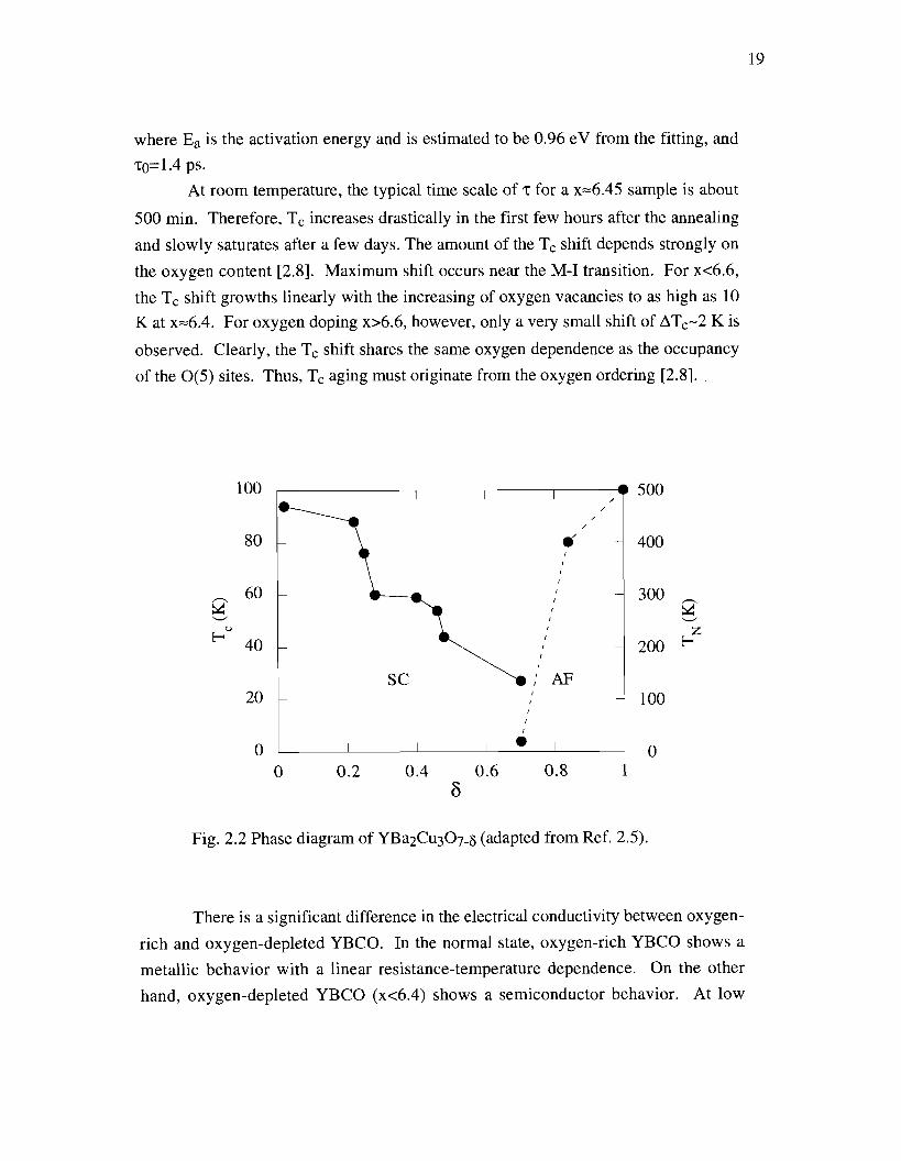
vacancies [2.5, 2.61. Figure 2.2 shows a typical phase diagram of the YBCO system.
Evidently, two plateaus of Tc appear, one at 60 K and the other at 90 K. The 60-K
and 90-K plateaus are commonly observed in YBCO samples, regardless the sample
preparation procedure, and are often referred to as the 60-K phase and the 90-K
phase, respectively. The 90-K phase exists for oxygen-rich YBCO (6.8<x<7.0)
whereas the 60-K phase occurs for partially doped YBCO (6.5<x<6.8). The transition
between the 60-K and 90-K phases is so sharp that samples with Tc in between are
difficult to prepare. Near x=6.4, metal-insulator (M-I) transition occurs in analogy
with the 0 - T transition. Below the transition (x<6.4), YBCO becomes
semiconducting or insulating at low temperatures.
YBCO samples with the intermediate Tc can be prepared by controlling the
oxygen content through a variety of annealing processes. Reliable annealing methods
in either oxygen or an oxygen-free atmosphere have been reported [2.7-2.131. Right
after the annealing, an aging of Tc is commonly observed at both low and room
temperatures [2.8]. During the aging process, Tc increases gradually with time. The
shift in Tc is found to follow a stretched-exponential equation
Tc(t) = Tc(m) - [Tc(m) - Tc(0)]exp[-(t/z)l/2] , (2. la)
and the characteristic time z is found to be governed by a thermally activated process
z = zoexp(Ea/kBT) , (2. lb)
where Ea is the activation energy and is estimated to be 0.96 eV from the fitting, and
20=1.4 ps.
At room temperature, the typical time scale of T for a x-6.45 sample is about
500 min. Therefore, Tc increases drastically in the first few hours after the annealing
and slowly saturates after a few days. The amount of the Tc shift depends strongly on
the oxygen content [2.8]. Maximum shift occurs near the M-I transition. For ~ ~ 6 . 6 ,
the Tc shift growths linearly with the increasing of oxygen vacancies to as high as 10
K at ~ ~ 6 . 4 . For oxygen doping x>6.6, however, only a very small shift of ATc-2 K is
observed. Clearly, the Tc shift shares the same oxygen dependence as the occupancy
of the O(5) sites. Thus, Tc aging must originate from the oxygen ordering [2.8].
Fig. 2.2 Phase diagram of YBa2C1.1307-6 (adapted from Ref. 2.5).
There is a significant difference in the electrical conductivity between oxygen-
rich and oxygen-depleted YBCO. In the normal state, oxygen-rich YBCO shows a
metallic behavior with a linear resistance-temperature dependence. On the other
hand, oxygen-depleted YBCO ( ~ ~ 6 . 4 ) shows a semiconductor behavior. At low

temperatures, its resistivity follows Mott's variable-range hopping (VRH) [2.13], with
the sheet resistivity higher than 10 MWsquare.
The theory of VRH developed by Mott has been applied to a broad range of
materials, including transition-metal oxides, sulfides, alkali-halides, and doped
semiconductors. It has successfully depicted another important category of
temperature dependence other than the thermally activated exponential processes.
Because of its importance in the transport of insulating YBCO, we briefly review the
Mott's VRH theory.
For two impurities separated by R in real space, the probability W of phonon-
assisted hopping due to acoustic phonons can be expressed as [2.13]
where AE is the average energy needed to hop to the nearest neighboring impurities.
If the electron hops a much larger distance (say pR with p>> I) , it has a choice
of pN as many sites, where N is the dimensionality. Therefore, it may find some sites
with energy much closer to its own. With an energy difference of AE/pN, the hopping
probability is
and the maximum probability corresponds to
If p is greater than unity, the VRH probability is no longer proportional to
exp(-AE~BT) but to
Correspondingly, the conductivity is expressed as
Therefore, the temperature dependence of the conductivity can be used to
distinguish between the thermal activated process and Mott's VRH.

2.3 Electronic structure
2.3.1 Theories
We have already mentioned that the most conlmon feature in HTS conlpounds
is the existence of two-dimensional CuO2 planes. Within the Cu02 planes, an
antibonding band is formed by the Cu-3d and 0-2p electrons. Generally, Cu02
planes are accepted as the conducting planes and the location for the Cooper pair
density [2.14]. According to the high-energy electron energy-loss spectroscopy, the
dominant bands in the CuO2 plane arise from the o-bonding between the C~-3d,2-~2
and 0 - 2 ~ ~ ~ ~ orbitals [2.15].
In semiconductors, band-diagram calculations using one-electron
approximation have successfully predicted their electronic properties. One-electron
approximation has also been applied to YBCO [2.16-2.191. For oxygen-rich YBCO,
the calculations yield a band structure consisting of two bands for the CuO2 plane and
two other bands for the Cu-0 chain. Although these calculations reproduced the
metallic behavior of oxygen-rich YBCO, they failed to predict the semiconducting
properties and the long-range antiferromagnetic ordering in undoped YBCO. The
latter fact suggests the strong correlation within the electronic system.
To account for the high electron correlation, Hubbard models based on spin
fluctuations were proposed for the band structure of HTS [2.20-2.221. Within the
framework of the Hubbard model, the electronic structure of the Cu02 plane is
modeled by a two-dimensional lattice consisting of Cu (3dx2_y2) and 0 (2px) or 0
(2py) electrons. The antiferromagnetic ordering originates from the half filling of the
Cu02 planes. Despite the controversy over the choice between the one-band [2.20]
and extended three-band [2.2 11 Hubbard models, the three-band Hubbard model has
been generally accepted in the field of optical excitations.
For the extended Hubbard model [2.21], both the diagonal and off-diagonal
terms are included in the Hamiltonian. The site-diagonal terms (Eii, Uii) are ( E ~ , Up)
and ( ~ d , Ud) for O(2p) and Cu(3d) states, respectively. The nonvanishing off-
diagonal terms &ij=ft and Uij=V are the hopping integrals and the interaction between
neighboring Cu and 0 sites, respectively.
Figure 2.3 plots a schematic of three-band Hubbard diagram for a YBCO
compound. The Cu-3d band is split by the on-site Coulomb repulsion into a upper
Hubbard band (UHB) and a lower Hubbard band (LHB). The 0-2p band resides
between the UHB and LHB. In undoped YBCO, the 0-2p band is fully occupied and

the Cu-3d UHB is empty. A charge-transfer (CT) gap ECT of about 1.75 eV separates
the 0-2p band and the Cu-3d UHB. Since the on-site Coulomb repulsion U-8 eV is
much larger than the CT energy A (U>>A), the undoped YBCO is defined as a
charge-transfer insulator [Fig. 2.3(a)] instead of a Mott-Hubbard insulator where
U<<A. The minimum energy for interband transitions across the CT gap is estimated
by E ~ ~ = ~ ( A ~ - 4t2)lt2 [2.2 1, 2.231.
7
DOS
(a) Undoped (b) Doped
Fig. 2.3. The Hubbard band model for the CuO2 plane in YBCO.
(a) x<6.4, and (b) x>6.5.
The Hubbard model has been successful in predicting the antiferromagnetic
ordering and semiconducting properties in oxygen-depleted YBCO. For doped
YBCO, however, the band structure is still a subject of continuing debate. Issues
regarding how the Hubbard bands vary with oxygen doping are unclear. If the
Hubbard bands are assumed to remain unchanged in the doped system (rigid-band

assumption), the Fermi level is predicted to move into the middle of the 0-2p band.
In this way, conducting holes are introduced to the Cu02 plane (Fig. 2.3b).
Moreover, the rigid-band assumption predicts that Fermi energy is a function of the
oxygen content. Therefore, experimental monitoring of the Fermi energy upon
oxygen doping will be insightful to understand the band model. Since the CT gap
energy is on the order of the visible light, optical investigations are considered the
most intuitive way to probe the CT band structure. Indeed, among the abundant
studies reported, most of them were related with the parent semiconducting phase of
YBCO where the band structure is best described by the Hubbard model.
2.3.2 Optical investigations
CT gap has been confirmed by a variety of experimental observations. In the
reflectance spectra of YBCO, a fundamental absorption peak near 1.75 eV was
observed at room-temperature in insulating YBCO [2.24]. Also observed was a
strong transition at 4.1 eV which is believed to come from several out-of-plane
transitions including intra-atomic transitions on the Cu(1) site, Cu(1)-O(4) transitions,
and Ba-O(4) excitations. Furthermore, the optical reflectance in the ab plane was
investigated with respect to the oxygen doping level [2.24]. In general, doping causes
a loss of spectral weight above the CT gap and a development of low-energy
absorption. The increase in plasma frequency was considered as an indication of the
increased effective numbers of electrons by doping. A linear relation was obtained
between the effective electron numbers and the oxygen content.
Raman scattering has been a powerful tool in studying the electronic structure
of YBCO. The long-range antiferromagnetic ordering in undoped YBCO was
verified by the resolved two-magnon feature at 2650-cm-I in the Raman spectra
[2.25-2.291. In a two-dimensional antiferromagnetic system, the interaction between
the spins and the excitation photon can be described by a three-step process [2.26]:
first, an electric-dipole transition of a Cu-d electron; then, a superexchange to a
neighboring Cu-d electron via oxygen; and finally, a second electric-dipole transition
emitting a photon. The strength of the two-magnon scattering arises from the two
subsequent spin flips. The exchange energy J=950 cm-l was also obtained from the
peak position of the two-magnon scattering [2.25]. Since two-magnon scattering
originates from the long-range antiferromagnetic ordering, it relies strongly on the
oxygen content in YBCO [2.26]. Its peak magnitude decreases with the increased
oxygen doping and disappears once the M-I transition is reached. (x=6.4). Moreover,

the two-magnon peak for YBCO near the M-I transition shows an aging behavior as a
result of oxygen ordering.
Besides two-magnon scattering, another high-order process, namely two-
phonon scattering, has also been observed in YBCO [2.27-2.291. The Raman shift for
the two-phonon scattering is nearly twice that of the fundamental phonons in
insulating YBCO.
Both two-magnon and two-phonon processes are sensitive to the excitation
energy. It was found that with excitations close to the CT gap, two-phonon peaks
were enhanced while the two-magnon peak was suppressed [2.28, 2.291. The strong
suppression of the two-magnon peak near the CT gap is consistent with the fact that
CT transition corresponds to carrier excitations from oxygen to copper and not
between the Cu UHB and LHB [2.28].
Resonant Raman scattering in insulating YBCO showed resonance features
near 1.7, 2.1, and 2.5 eV which were assigned to the in-plane CT excitations [2.30].
Corresponding band diagrams based on the extended Hubbard model have been
developed for both the undoped and oxygen-rich YBCO.
A strong Raman feature with Azg symmetry has been resolved near the CT
gap [2.31]. From the symmetry point of view, it has been assigned to either intra-
atomic transitions between the Cu-d orbitals (dxLy2 to dxy) or photon-assisted d to po
transition followed by photon-assisted po to p, hole hopping. In the latter case, a
linear combination of neighboring p, holes is required to attain the correct phase
match with the center dx2-y2 hole. Moreover, the A2g feature displays a dependence
on the oxygen content. The distinct peak at x-6.1 remains nearly unchanged until
oxygen doping reaches x-6.3. Once x>6.6, the A2g peak disappears.
Further, the Raman spectrum excited at 1.16 eV displays a group of three
features which are sensitive to oxygen doping. With the increase of oxygen content,
the center peak at 507 cm-1 becomes dominant and associates with several overtones.
The shift and strength variation is assigned to Ag vibration of the apex O(4) atoms
adjacent to the O(1) sites which are filled upon doping [2.32].
Beside Raman scattering, other optical investigations have also been
performed on YBCO. Photoluminescence (PL) has resolved deep intragap states in
semiconducting YBCO [2.32]. With a 2.54 eV excitation, a midgap PL emission was
observed near 1.3 eV. The PL peak dropped significantly when the oxygen content
increased from x-6.0 to x-6.15. Recombination between the exciton level below the
UHB and the deep intragap states are believed to be responsible for the PL emission.

A band model based on the above investigation has been proposed for undoped
YBCO.
Photoconductivity studies of insulating YBCO have observed similar spectral
features near 1.75, 2.7, and 4.2 eV as that of optical conductivity [2.33, 2.341. The coincidence between the photoconductivity and optical conductivity spectra implies
that CT transition results in mobile carriers (separate charges) rather than neutral
excitons. In addition, the 1.5-eV feature resolved in low-temperature
photoconductivity determines the lowest interband CT transition. The 1.5-eV feature
is found to exist over a broad oxygen range for 6.0cxc6.3.
While optical conductivity still demonstrates a strong peak at 1.7 eV for
YBCO with oxygen content x-6.3, the photoconductivity is weak below 2 eV [2.33].
It is concluded that electronic states involving the 1.5- and 1.7-eV transitions are
localized for ~ ~ 6 . 3 - 6 . 4 . Consequently, CT insulator, Fermi glass, and metallic band
diagrams have been proposed for oxygen-depleted, intermediate doping level, and
oxygen-rich YBCO systems, respectively. Moreover, transient photoconductivity
investigations showed that photoexcited carriers in insulating YBCO have lifetime on
the order of 10 ns [2.34].
In addition to oxygen doping, an increase in carrier density can be achieved
via photodoping of oxygen-poor YBCO. Photodoping has been observed in YBCO
system over a broad range of oxygen contents (6.35cxc6.70) [2.35-2.391. The
resistivity of YBCO was found to decrease substantially under the exposure of visible
light. Such a decrease in resistivity persists at low temperatures. Prolonged light
irritation leads to the full loss of resistivity or an enhancement in Tc. The relaxation
of the photodoping effect has been found to follow a stretched-exponential decay
[2.35]:
where T is the characteristic decay time, P is the dispersion parameter.
The dispersion parameter can be well fitted with an empirical linear function
between temperatures of 270 and 330 K
The characteristic decay time can be described by thermally activated
relaxation across an energy barrier as [2.35]

where activation energy E,=0.935 eV, and ~0=1.4 ps. Coincidentally, these values are
very close to that obtained from investigations on the T, aging and oxygen ordering
(see Sec. 2.2).
From the value of p obtained in the photodoping effect, the width of the trap
distribution in the sample was estimated by Eq. (2.8a) to be -0.1 eV [2.35].
Currently, there are two competing mechanisms proposed for photodoping:
photoinduced charge transfer [2.35] and photo-assisted oxygen ordering [2.3, 2.351.
The first mechanism emphasizes the photoexcitation inside the Cu02 plane. The
excited electrons are transferred to the adjacent CuO chains and trapped in the
localized 0 - levels. As a consequence, unpaired photoinjected holes contribute to the
total concentration of free holes in the Cu02 planes. Oxygen ordering mechanism
favors photoexcitation within the CuO, chain layer. Photo assisted oxygen defect
ordering tends form longer chain segments. The result is the charge transfer of
additional holes to the Cu02 plane. As in the previous case, an increase in the sample
conductivity is expected.

References
Crystal Structure
[2.1] A. Santoro, "Crystallography: the system Ba2MCu30g (M = Y, Gd, Eu, etc.),"
in High Temperature Superconductivity, edited by J. W. Lym, (Springer-
Verlag, New York), p. 105, 1990
Oxygen Ordering
[2.2] N. Chandrasekhar, 0 . T. Valls, and A. M. Goldman, "Charging effects
observed in YBa2C~307-~ films: influence of oxygen ordering," Phys. Rev. B
39,6619 (1989)
[2.3] G. Nieva, E. Osquiguil, J . Guimpel, M. Maenhoudt, B. Wuyts, Y.
Bruynseraede, M. B. Maple, and I. K. Schuller, "Photoinduced enhancement
of superconductivity," Appl. Phys. Lett. 60,2159 (1992)
[2.4] E. Osquiguil, M. Maenhoudt, B. Wuyts, Y. Bruynseraede, D. Lederman, and
I. K. Schuller, "Photoexcitation and oxygen ordering in YBa2Cu30x films,"
Phys. Rev. B 49,3675 (1994)
Phase Diagram
[2.5] J. Zaanen, A. T. Paxton, 0 . Jepsen, and 0 . K. Andersen, "Chain-fragment
doping and the phase diagram of YBa2C~307-~," Phys. Rev. Lett. 60, 2685
(1988)
[2.6] J. D. Jorgensen, B. W. Veal, A. P. Paulikas, L. J. Nowicki, G. W. Crabtree, H.
Claus, and W. K. Kwok, "Structural properties of oxygen-deficient
YBa2Cu307-g ," Phys. Rev. B 41, 1863 (1990)
Oxygen Annealing
[2.7] P. K. Gallagher, "Characterization of Ba2YCu30x as a function of oxygen
partial pressure I. thermoanalytical measurements," Adv. Cer. Mater. 2, 632
(1987)
[2.8] B. W. Veal, H. You, A. P. Paulikas, H. Shi, Y. Fang, and J. W. Downey,
"Time-dependent superconducting behavior of oxygen-deficient YBa2Cu30x:
possible annealing of oxygen vacancies at 300 K," Phys. Rev. B 42, 4770
(1990); B. W. Veal, A. P. Paulikas, H. You, H. Shi, Y. Fang, and J. D.
Downey, "Observation of temperature-dependent site disorder in YBa2Cu307-
g below 150 OC," Phys. Rev. B 42,6305 (1990)

[2.9] E. Osquiguil, M. Maenhoudt, B. Wuyts, and Y. Bruynseraede, "Controlled
preparation of oxygen deficient YBa~Cu30, films," Appl. Phys. Lett. 60,
1627 (1992)
[2.10] P. Meuffels, B. Rupp, and E. Porschke, "Physical and structural properties of
YBa2Cu30, prepared by a defined oxygen sorption technique," Physica C
156,441 (1988)
[2.11] D. Shi and D. W. Capone, "60-90 K superconducting phase transition in
YBa2Cu307-6," Appl. Phys. Lett. 53, 159 (1988)
[2.12] E. Takayama-Muromachi, Y. Uchida, M. Ishii, T. Tanaka, and K. Kato, "High
Tc superconductor YBa2Cu30y -oxygen content vs Tc relation-," Jpn. J. Appl.
Phys. 26, L 1 156 (1987)
Variable-range Hopping
[2.13] N. F. Mott, "Conduction in non-crystalline materials 111. localized states in a
pseudogap and near extremities of conduction and valence bands," Phil. Mag.
19, 835 (1969); "Conduction in glasses containing transition metal ions," J.
Non Cryst. Solid 1, 1 (1968)
Band Structure
[2.14] R. C. Dynes, "The order parameter of high Tc superconducors: experimental
probes," Solid State Commun. 92,53 (1994)
[2.15] N. Niicker, H. Romberg, X. X. Xi, F. Fink, B. Gegenheimer, and Z. X. Zhao,
"Symmetry of holes in high-Tc superconductors," Phys. Rev. B 39, 6619
(1989)
[2.16] See W. E. Pickett, "Electronic structure of the high-temperature oxide
superconductors," Rev. Mod. Phys. 61,433 (1989) and references there after.
[2.17] S. Massidda, J. Yu, A. J. Freeman, and D. D. Koelling, "Electronic structure
and properties of YBa2Cu307-6, a low dimensional, low density of states
superconducor," Phys. Lett. A 122, 198 (1987)
[2.18] J. Yu, S. Massidda, A. J. Freeman, and D. D. Koelling, "Bonds, bands, charge
transfer excitations and superconductivity of YBa2Cu307-6," Phy s. Lett. A
122,203 (1987)
[2.19] L. F. Mattheiss and D. R. Hamann, "Electronic structures of high Tc
superconducting Ba2YCu306.9," Solid State Comrnun. 63, 395 (1987)
Hubbard Models
[2.20] P. W. Anderson, "The resonating valence bond state in LazCu04 and
superconductivity," Science 235,96 (1987)

[2.21] V. J. Emery, "Theory of high-Tc superconductivity in oxides," Phys. Rev.
Lett. 58,2794 (1987)
[2.22] S. Uchida, T. Ido, H. Takagi, T. Arima, Y. Tokura, and S. Tajima, "Optical
spectra of La2-,SrXCu04: effect of carrier doping on the electronic structure of
the Cu02 plane," Phys. Rev. B 43,7942 (1991)
[2.23] C. A. Balseiro, M. Avignon, A. G. Rojo, and B. Alascio, "Electronic
Properties of High-T, superconductors," Phys. Rev. Lett. 62, 2624 (1989)
Optical Reflectance
[2.24] S. L. Cooper, D. Reznik, A. Kotz, M. A. Karlow, R. Liu, M. V. Klein, W. C.
Lee, J. Giapintzakis, and D. M. Ginsberg, "Optical studies of the a-, b-, and c-
axis charge dynamics in YBa2C~306+~," Phys. Rev. B 47, 8233 (1993)
Raman Scattering
[2.25] K. B. Lyons, P. A. Fleury, L. F. Schneemeyer, and J. V. Waszczak, "Spin
fluctuations and superconductivity in Ba2YCu306+&," Phys. Rev. Lett. 60,
732 (1988)
[2.26] A. A. Maksimov, I. I. Tartakovskii, M. V. Klein, and B. W. Veal, "Two-
magnon light scattering in YBa2C~306+~ single crystals near the metal-
insulator transition," Phys. Rev. B 49, 15385 (1994)
[2.27] C. Thomsen, E. Schonherr, B. Friedl, and M. Cardona, "Identification of the
1250-~rn-~ Raman feature in YBa2Cu306," Phys. Rev. B 42, 943 (1990)
[2.28] M. Yoshida, S. Tajima, N. Koshizuka, S. Tanaka, S. Uchida, and T. Itoh,
"Two-magnon and two-phonon excitations in some parent insulating
compounds of high-Tc cuprates," Phys. Rev. B, 46,6505 (1992)
[2.29] M. V. Klein, R. Liu, D. Salamon, S. L. Cooper, W. C. Lee, D. M. Gindberg,
and S. W. Cheong, "New features of Mott-Hubbard insulator gap of parent
HTS compounds found by resonance Raman scattering and UV-excited
ordinary Raman scattering," J. Supercond. 7,429 (1994)
[2.30] E. T. Heyen, J. Kircher, and M. Cardona, "Resonant Raman scattering in
insulating YBa2Cu306 as a probe of its electronic structure," Phys. Rev. B 45,
3037 (1992)
[2.31] R. Liu, D. Salamon, M. V. Klein, S. L. Cooper, W. C. Lee, S-W. Cheong, and
D. M. Ginsberg, "Novel Raman-active electronic excitations near the charge-
transfer gap in insulating cuprates," Phys. Rev. Lett. 71, 3709 (1993)
Photoluminescence [2.32] V. N. Denisov, C. Taliani, A. G. Mal'shukov, V. M. Burlakov, E. Schonherr,
and G. Ruani, "Infrared-excited Raman scattering and photoluminescence of

deep intragap states in semiconducting YBa2Cu306+,," Phys. Rev. B 48,
16714 (1993)
Photoconductivity
[2.33] G. Yu, C. H. Lee, D. Mihailovic, A. J. Heeger, C. Fincher, N. Herron, and E.
M. McCarron, "Photoconductivity in insulating YBa2Cu306+,: from Mott-
Hubbard insulator to Fermi glass via oxygen doping," Phys. Rev. B 48, 7545
( 1993)
[2.34] G. Yu, A. J. Heeger, G. Stucky, N. Herron, and E. M. McCarron, L. Cong, G.
C. Spalding, C. A. Nordman, and A. M. Goldman, "Phase separation of
photogenerated carriers and photoinduced superconductivity in high-Tc
materials," Phys. Rev. B 45,4964 (1992)
Photodoping and Persistent Photoconductivity
[2.3] G. Nieva, et al. ibid.
[2.4.] E. Osquiguil, et al. ibid.
[2.35] V. I. Kudinov, I. L. Chaplygin, A. I. Kirilyuk, N. M. Kreines, R. Laiho, E.
Lahderanta, and C. Ayache, "Persistent photoconductivity in YBa2Cu306+,
films as a method of photodoping toward metallic and superconducting
phases," Phys. Rev. B 47,9017 (1993)
[2.36] S. L. Bud'ko, H. H. Feng, M. F. Davis, J. C. Wolfe, and P. H. Hor, "Persistent
photoconductivity in insulating and superconducting YBa2Cu30, thin films:
temperature and spectral dependence," Phys. Rev. B 48, 16707 (1993)
[2.37] K. Tanabe, S. Kubo, F. H. Teherani, H. Asano, and M. Suzuki, "Effects of
photoinduced hole doping on normal-state and superconducting transport in
oxygen-deficient YBa2Cu30y," Phys. Rev. Lett. 72, 1537 (1994)
[2.38] J. Hasen, D. Lederman, I. Schuller, V. Kudinov, M. Maenhoudt, and Y.
Bruynseraede, "Enhancement of persistent photoconductivity in insulating
high-T, thin films," Phys. Rev. B 51, 1342 (1995)
[2.39] G. Yu, A. J. Heeger, G. Stucky, N. Herron, and E. M. McCarron, "Transient
photoinduced conductivity in semiconducting single crystals of YBa2Cu306.3:
search for photoinduced metallic state and for photoinduced
superconductivity," Solid State Commun. 72, 345 (1989)
3 Fabrication of YBCO Thin Films with Different Oxygen Contents
3.1 Overview of different deposition methods
Deposition of HTS thin films using all major physical vapor deposition (PVD)
and chemical vapor deposition (CVD) techniques has been widely studied [3.1-3.281.
Depending on whether post annealing after the film growth is necessary or not, the
deposition techniques are divided into in-situ and ex-situ methods. For multi-source
processes such as vacuum evaporation [3.4, 3.51 and metal-organic chemical vapor
deposition (MOCVD) [3.6-3.111, subsequent high-temperature annealing is
mandatory and more important than the deposition process itself. Ex-situ methods
have been used to produce nearly all known HTS thin films. Moreover, thin films of
Bi-Sr-Ca-Cu-0 and T1-Ba-Ca-Cu-0 families are found to be readily possible to
fabricate only by ex-situ techniques.
The main advantage of the in-situ growth is that no post annealing is needed
to rearrange the lattice structure of as-deposited films. The in-situ process produces
thin films with minimum contamination and with a single-crystal structure on
epitaxial substrates. Hence, in situ deposition results in films of the highest quality.
Laser ablation [3.12-3.181 and sputtering [3.19-3.281 are the most often used in-situ
PVD techniques. For both methods, substrates must be heated to temperatures above
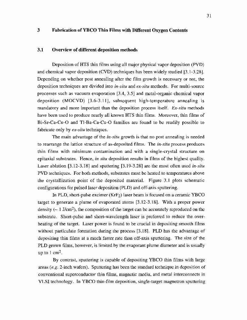
the crystallization point of the deposited material. Figure 3.1 plots schematic
configurations for pulsed laser deposition (PLD) and off-axis sputtering.
In PLD, short-pulse excimer (KrF2) laser beam is focused on a ceramic YBCO
target to generate a plume of evaporated atoms [3.12-3.181. With a proper power
density (- 1 J/cm2), the composition of the target can be accurately reproduced on the
substrate. Short-pulse and short-wavelength laser is preferred to reduce the over-
heating of the target. Laser power is found to be crucial in depositing smooth films
without particulate formation during the process [3.18]. PLD has the advantage of
depositing thin films at a much faster rate than off-axis sputtering. The size of the
PLD grown films, however, is limited by the evaporant plume diameter and is usually
up to 1 cm2.
By contrast, sputtering is capable of depositing YBCO thin films with large
areas (e.g. 2-inch wafers). Sputtering has been the standard technique in deposition of
conventional superconductor thin films, magnetic media, and metal interconnects in
VLSI technology. In YBCO thin-film deposition, single-target magnetron sputtering

has proven to be a simple and reliable process. Both dc and rf sputtering methods
have been used to deposit high quality YBCO films.
Heater - Target
Target Heater
(a) Laser ablation (b) Off-axis sputtering
Fig. 3.1 Schematics configurations for (a) PLD, and (b) off-axis
sputtering methods.
Low deposition rate of sputtering arises from the difficulty in obtaining the
stoichiometry of deposited films exactly the same as that of the target. Due to
preferential backsputtering by negative oxygen ions, stoichiometry of the sputtered
YBCO films may be different from the target composition [3.23]. Such a deviation in
composition causes a significant degradation in the superconducting properties of
YBCO films.
In principle, it is always possible to offset the effects of preferential
backsputtering by modifying the target composition, but this approach leads to a
complicated stoichiometry dependence on sputtering parameters. Hence, modifying
target composition is not a practical method for reliable deposition of YBCO films.
Instead, other approaches, such as the increase of the sputtering pressure or special
target-substrate configurations, have proven to be much easier to implement.
High pressure sputtering is preferred to reduce the backsputtering. The
efficient scattering of energetic particles by the sputtering gas greatly lowers the
bombardment energy. In a parallel target-substrate orientation, high quality YBCO

films with Tc=90 K were obtained by high pressure sputtering [3.25]. However, the
drawbacks of the high-pressure sputtering include a very low deposition rate and
potentially unstable plasma (arcing). Moreover, high-pressure sputtering causes a
heavy load for vacuum pumps, e.g., requiring frequent regeneration of cryopumps.
Alternatively, special target-substrate configurations such as off-axis
sputtering and negative-ion shields were designed to minimize the impact of
preferential backsputtering. In the off-axis configuration, a substrate is placed outside
the region of sputtering plasma [see Fig. 3.l(b)]. Direct bombardment of energetic
particles is avoided at the expense of the deposition rate. Despite its extremely low
deposition rate, off-axis sputtering has been used to deposit YBCO films with the
highest TC's and JC's.
In addition to the off-axis sputtering, a configuration using a negative-ion
shield has also proven to be a reliable method of depositing YBCO with excellent
properties [3.26]. In this case, a negative-ion shield is placed above the target center
to reduce the bombardment and the substrate is placed inside the magnetron erosion
ring. Due to its parallel target-substrate orientation, this approach has a deposition
rate much higher than the off-axis sputtering.
Correct gas ratio between argon and oxygen is also an important parameter to
obtain high quality YBCO films [3.25]. Sputtering in pure oxygen is capable of
depositing high quality films. However, it leads to slightly Y-rich composition on the
surface of the target. On the other hand, pure argon sputtering results in very Y-rich
films which are not superconducting and require ex-.situ annealing. The degraded
target due to long-time sputtering in pure argon could be fully recovered once the
sputtering gas is switched to pure oxygen. For mixed sputtering gases, the argon to
oxygen ration below 10:1 is recommended in order to obtain YBCO films with the
high TC's and JC's.
Crystal structure of the target also influences the quality of sputtered YBCO
films. Thin films deposited using tetragonal (nonsuperconducting) targets display a
degraded T, [3.25]. In contrast, orthorhombic targets lead to films with excellent
superconducting properties. The contrast is related to the difference in the embedded
active oxygen atoms in tetragonal and orthorhombic targets. During the deposition,
the stabilization of the orthorhombic phase is very sensitive to the amount of oxygen
available. Insufficient oxygenation leads to films with degraded TC's. Moreover, it is
well known that active oxygen atoms are much more efficient than molecular oxygen
in forming the orthorhombic phase [3.4, 3.5, 3.301. One of the sources for active
oxygen atoms is the target itself. For the orthorhombic target, the embedded active

oxygen is adequate to assist the orthorhombic formation on the substrate. For the
tetragonal target, however, much less active oxygen is available. Oxidation has to
rely on oxygen from the sputtering gas. As a result, degraded YBCO films with a less
orthorhombic structure are obtained.
Substrates selection is another key issue for high-quality HTS films growth.
General requirements for the substrates include good mechanical property, low cost
and chemical stability. In addition, epitaxial growth demands good lattice and
thermal expansion match between the substrate and thin film. Commonly used
substrates for YBCO deposition are MgO, LaA103, and SrTi03. Among them,
SrTi03 and LaA103 provide YBCO films with the best TC's, JC's, and sharp
superconducting transition widths. Unfortunately, a large dielectric constant (E-300)
of SrTi03 is inappropriate for high-frequency applications. On the other hand, MgO
has a much smaller dielectric constant (E-10) and is suitable for high-frequency
applications. Further, MgO is much cheaper than SrTi03 or LaA103. In terms of
thermal conductivity, MgO is also a better thermal conductor than LaA103 and
SrTi03. On the other hand, LaA103 substrates provide a better epitaxial conditions
than MgO and enable deposition of very high quality films. At the same time, the
dielectric constant of LaA103 is comparable with that of MgO. Table 3.1 lists
properties of commercially available SrTi03, LaA103, and MgO substrates [3.46]
Table 3.1 Physical Properties of Single-Crystal Substrates for HTS [3.46]
Substrate YBCO Lattice Dielectric Loss
Mismatch Constant tan6
3 10 (300 GHz) 3x 1 0-2 (300 GHz)
20 (700 GHz) 8x10⁻³ (700 GHz)
9.9 (300 GHz) 1x1 0-3 (300 GHz)
Preheating of the substrate above the crystallization temperature of YBCO
(600-900 OC) is essential to growth high quality thin films using PVD. High substrate
temperature is necessary to produce c-axis oriented films [3.29-3.3 11. At
temperatures lower than 650 OC, formation of a degraded phase with a-axis

orientation takes place. Furthermore, high temperature is preferred for sufficient
oxygenation [3.32].
3.2 Thin-film characterization
Proper stoichiometry of YBCO films is crucial for attaining good
superconducting properties. It can be determined using the non-destructive energy
dispersive x-ray analysis (EDX). With proper calibration, EDX is capable of
detecting the composition with high accuracy. For oxygen diffusion studies,
secondary ion mass spectroscopy (SIMS) is used to trace tiny variations in oxygen
stoichiometry.
X-ray diffraction (XRD) is the most common technique for determining the
film crystalline structure. It provides information about the preferred orientation and
lattice constants normal to the film surface. Also, the uniformity of c-axis orientation
is reflected in the sharpness of the 28 peak.
Transmission electron microscopy (TEM) is another powerful tool in defining
the crystallographic relations. The diffraction patterns of TEM contain enriched
information about the crystal orientation, phase, defects, and grain boundaries, which
play an important role in the fabrication of HTS Josephson junctions. Furthermore,
the high magnification of TEM also permits detection of submicron features which
are invisible by other techniques.
In YBCO thin films, the most common defects revealed by TEM are
dislocations and twinning at the fildsubstrate interface which originate from
mismatch between YBCO and the substrate [3.25]. Such defects are intrinsic to all
kinds of epitaxial growth and hence directly indicate the imperfection of epitaxy. The
second major source of defects are the second-phase particles with structures other
than "123". TEM is capable of resolving these particles even in the case when they
are too sparse to be detected by EDX. Formation of second-phase structures is also
responsible for the stacking fault observed in the cross-section TEM images of c-axis
oriented films.
For investigating surface morphology of films, scanning electron microscopy
(SEM) is widely used. Advanced SEM has even the ability of performing cryogenic
testing at the liquid nitrogen temperature (77 K).

3.3 RF magnetron sputtering YBCO thin films
YBCO thin films studied in this thesis were fabricated by in-situ RF
magnetron sputtering [3.25]. The best YBCO thin films were deposited on LaA103
substrates using off-axis configuration (deposited by Dr. J. Gavaler at the
Westinghouse Science and Technology Center). These films displayed an extremely
sharp, about 0.5-K wide (10-90%) superconducting transition width, high zero-
resistance critical temperature Tco of 89.5 K and J, above 2 ~ A . / c m 2 at 77 K. We
have also performed in-house sputtering of YBCO thin films on polished LaA103,
SrTi03 and MgO substrates, using CVC's SC8000 RF magnetron sputtering system.
These films exhibited Tco's between 84 K and 89 K with ATc of 1-2 K. The
thickness of our YBCO films ranged from 80 to 300 nm. A composite YBCO target
was used for rf sputtering. Substrates were preheated to approximately 750 OC and
stabilized prior to deposition. The sputtering gas consisted of 10 mTorr of Ar and 5 mTorr of 0 2 . A negative-ion shield of 3 inches in diameter was placed above the
target to reduce the back etching of our films. The spacing between the target and the
substrate was 1-314 inches. The rf power output was 450 W and zero reflection was
achieved by automatic impedance matching. Presputtering was applied to minimize
possible contamination from the target surface. The deposition rate was about 35
BVmin.
Either 90-K or semiconducting YBCO films were deposited by the above
method. For fully oxygenated (90-K) samples, as-deposited films were in situ
annealed in 100 mTorr of 02 . Conversely, fully oxygen-depleted (semiconducting)
films were obtained by in-situ annealing in 100 mTorr of Ar. Oxygen-depleted
YBCOIMgO samples were prepared by for femtosecond pump-probe investigations.
3.4 Annealing of YBCO thin films
Besides the in-situ annealing following the deposition, YBCO thin films can
be ex-situ annealed to achieve various oxygen contents. Various annealing methods
have been reported for preparing YBCO samples with the desired oxygen content
[3.33-3.381. For annealing in oxygen atmosphere, the oxygen pressure-temperature
phase diagrams were obtained [3.33-3.351. These phase diagrams have been used as a
guide for dependable control of the oxygen content inside YBCO. Other annealing
methods include controlled oxidation of insulating YBCO at high temperatures

[3.36], constant-temperature annealing in controlled time [3.37], and quenching from
high temperature into liquid nitrogen [3.38].
The oxygen stoichiometry of our samples was modified either by furnace
annealing or by radiative heating in vacuum. Specifically, oxygen-depleted samples
for laser writing were prepared by deoxygenating the superconducting films inside a
vacuum chamber. The YBCO-on-LaA103 films were heated to 650 OC in 15 mTorr
Ar. Partially oxygen-deficient samples for femtosecond pump-probe experiments
were also vacuum annealed. The heating temperatures were 400, 365, and 340 OC for
YBCOLaA103 samples with Tc of 30 K, 55 K, and 60 K, respectively. Constant
dwell time of 1 hour was maintained during the annealing process.
Furnace annealing was also applied to decrease or recover the oxygen content
in YBCO films. Although furnace annealing is less clean (often results in surface
contamination) than the vacuum process, it is much more convenient to operate.
Continuous flow of ultra pure Ar or 0 2 gas was guided through the oven for
removing or restoring oxygen, respectively.
3.5 Electrical measurements
The resistivity and critical current density versus temperature, R(T) and Jc(T),
curves were measured in a standard four-probe geometry. To ensure good ohmic
contacts, silver contact pads of 300-nm thick were vacuum evaporated directly on top
of our test structures. Aluminum wires were wire bonded to electrically connect the
contact pads with corresponding leads in the testing probe. The samples were placed
on a cold finger inside the probe, which was cooled down by liquid nitrogen or liquid
helium. The temperature and the cooling process were computer monitored by a
~akeshore@ temperature controller. Data acquisition was achieved by using
customized ~ a b v i e w @ programs.
Electrical transport of YBCO thin films with various oxygen contents was
tested. The R(T) curves for superconducting samples with TC7s of 89.5 K, 60 K, 55
K, 30 K and a semiconducting film are shown in Fig. 3.2. To assure enough Tc aging
of the intermediately doped YBCO, cryogenic testing was performed at least 1 day
after the annealing. Thus, further shift in T, was considered negligible.
The grain boundary characteristics can be reflected by the slope of the normal
state R(T) curves. While films with TC7s above 55 K exhibit nearly zero resistance at
zero temperature (extrapolation), the 30-K film shows a large positive zero-

temperature resistance intercept. It is well known that the positive zero-temperature
resistance offset originates from high-angle grain boundaries in the film [3.39].
Therefore, the nearly zero offset for samples with Tc above 55 K indicates well
aligned grain boundaries in these films. As opposite to that, the big zero-resistance
offset in the 30-K sample implies the large content of high-angle grain boundaries.
Moreover, the sharp transitions for samples with Tc255 K suggest that oxygen
was distributed relatively homogeneously in these films [3.35]. By contrast, the
broad transition in 30-K sample indicates an inhomogeneous oxygen distribution.
Hence, the 30-K sample is considered a mixture of the semiconducting and the
superconducting phases. A significant rounding of the transition for the 30-K sample
is probably related to increased two-dimensional fluctuations [3.40-3.4 1 1.
0 40 80 120 160 200
Temperature (K)
Fig. 3.2 Resistivity vs. temperature for sputtered YBCO films with
with various oxygen doping levels.
The magnitude of the temperature-dependent resistance, on the other hand,
indicates the defect density in the grains. Despite potential difference in the contact
resistance, a significant increase in the 300-K resistance from the 90-K to 30-K was
observed. This fact indicates an increasing defect density towards the M-I transition
and is consistent with the expectation that perfect crystal structures correspond to

either oxygen-poor or fully oxygenated films. Maximum lattice distortion is expected
near the M-I phase transition.
As shown in Fig. 3.2, the resistance of a semiconducting sample increased
strongly at low temperatures and exceeded 10 MQIsquare below 100 K. The
temperature dependence of semiconducting YBCO cannot be fitted by a simple
exponential law that corresponds to thermal activation of localized states. Instead, it
follows Mott's VRH [3.42]. Figure 3.3 replots the resistance data from the
semiconducting sample in Fig. 3.2 and fits to the formalism of VRH. For the defect
states inside the bandgap, conducting current could be formed either by multiple
trapping or by electron tunneling between the localized states in the same direction
(hopping). The tunneling rate is a sensitive function of the intersite distance and the
energy separation between these states. A schematic diagram of trapping and hopping is plotted in Fig. 3.4. As indicated in Chapter 2, the dc conductivity o for
Mott's VRH is proportional to T-l/(N+l), where N is the number of dimensions
involved in the hopping process.
Fig. 3.3 ln[R(T)/R(217 K)] vs. T-114 for the semiconducting sample
shown in Fig. 3.2. The linear fit shows a variable-range hopping.

Evidently, the resistance of our semiconducting sample in Fig. 3.3 follows
closely to the T - ~ / ~ behavior. As a result, the low-temperature transport of
semiconducting YBCO can be concluded as a 3-dimensional VRH.
Band states
x - - - - - - - Trapping - - a - and release
A - -
Localized states
Fig. 3.4 Schematic diagram of transport with trapping and hopping [3.43].
3.6 Microfabrication
Photolithography and lift-off procedures were applied for patterning of our
YBCO microstructures. These patterns include YBCO microbridges designed for
critical-current measurements and ultrafast optoelectrical response tests on a double-
bridge configuration [3.44]. Microstrip lines and coplanar waveguides [3.45] were
also lifted off for testing of the photoconductive performance of YBCO thin films.
Figure 5.5 shows a typical flow chart of our lift-off procedure.
3.7 Summary
RF magnetron sputtering has been used for depositing our high quality YBCO
thin films. Sputtering configuration and parameters are crucial to the deposition
process. Off-axis and negative-ion shield configurations are the two approaches that
can efficiently eliminate the preferential backsputtering of freshly deposited thin
films. Both semiconducting and superconducting (with high Tc and sharp
superconducting transitions) YBCO thin films have been deposited by in-situ RF

magnetron sputtering. YBCO films with different oxygen contents have been
successfully prepared by either vacuum or furnace annealing methods. The electrical
properties of YBCO thin films were measured by cryogenic testing.
Wet etch and photo lift-off procedures were also used to pattern microbridges
and coplanar transmission lines on YBCO films.
Photoresist UV exposure 1400-27,60 sec.
75 OC, 20 min.
Metalization Lift-off
evaporation) soak in acetone
Overdevelop (Developer 452) 3 min.
Fig. 3.5 Flow chart of our lift-off procedure for patterning of YBCO circuits.
+ 4- Dry in N2 Soak in C6H5C1 (Chlorobenzene) 10 min.

References
Fabrication Review
[3.1] R. G. Humphreys, J. S. Satchell, N. G. Chew, J. A. Edwards, S. W. Goodyear,
S. E. Blenkinsop, 0. D. Dosser, and A. G. Cullis, "Physical vapour deposition
techniques for the growth of YBa2Cu307 thin films," Supercond. Sci.
Technol. 3,38 (1990)
[3.2] R. Simon, "High-T, thin films and electronic devices," Phys. Today, June p.
64, 1991
[3.3] X. X. Xi, T. Venkatesan, Q. Li, X. D. Wu, A. Inam, C. C. Chang, R. Ramesh,
D. M. Hwang, T. S. Ravi, A. Findikoglu, D. Hemmick, S. Etemad, J. A.
Martinez, and B. Wilkens, "Preparation of thin film high temperature
superconductors," IEEE Trans. Magn. MAG-27, 9982 (1991)
Vapor Evaporation
[3.4] N. Missert, R. Hammond, J. E. Mooj, V. Matijasevic, P. Rosenthal, T. H.
Geballe, A. Kapitulnik, M. R. Beasley, S. S. Laderman, C. Liu, E. Garwin, ,
and R. Barton, "In situ growth of superconducting YBaCuO using reactive
electron-beam coevaporation," IEEE Trans. Magn. MAG-25,2418 (1989)
[3.5] T. Terashima, Y. Bando, K. Iijima, K. Yamamoto, and K. Hirata, "Epitaxial
growth of Y B a 2 C ~ 3 0 7 - ~ thin films on (110) SrTi03 single crystals by
activated evaporation," Appl. Phys. Lett. 53,2232 (1988)
MOCVD
[3.6] K. Zhang, B. S. Kwak, E. P. Boyd, A. C. Wright, and A. Erbil, "c-axis
oriented YBa2C~307-~ superconducting films by metalorganic chemical vapor
deposition," Appl. Phys. Lett. 54, 380 (1989)
[3.7] D. S. Richeson, B. W. Wessels, J. Zhao, J. M. Zhang, H. 0 . Marcy, T. J.
Marks, L. M. Tonge, and C. R. Kannewurf, "Organometallic chemical vapor
deposition routes to high T, superconducting T1-Ba-Ca-Cu-0 films," Appl.
Phys. Lett. 54,2154 (1989)
[3.8] K. Zhang, E. P. Boyd, B. S. Kwak, A. C. Wright, and A. Erbil, "Metalorganic
chemical vapor deposition of T12CaBa2Cu20y superconducting thin films on
sapphire," Appl. Phys. Lett. 55, 1258 (1989)
[3.9] G. Malandrino, D. S. Richeson, T. J. Marks, D. C. DeGroot, J. L. Schindler,
and C. R. Kannewurf, "Phase-selective route to high Tc superconducting

T12Ba2Can-1CunQn+4 films: combined metalorganic chemical vapor
deposition using an improved barium precursor and stoichiometry-controlled
thallium vapor diffusion," Appl. Phys. Lett. 58, 182 (1991)
[3.10] K. H. Young, M. Robinson, G. V. Negrete, J. Zhao, C. S. Chern, Y. Q. Li, and
P. E. Norris, "Microwave resonators from YBa2Cu307-6 thin films made by
plasma-enhanced metalorganic chemical vapor deposition," Appl. Phys. Lett.
61, 543 (1992)
[3.11] Z. Lu, J. K. Truman, M. E. Johansson, D. Zhang, C. F. Shih, G. C. Liang,
"Large area double-sided YBa2Cu307-6 films grown by single-source metal-
organic chemical vapor deposition," Appl. Phys. Lett. 67,712 (1995)
Pulsed Laser Ablation
[3.12] X. D. Wu, A. Inam, T. Venkastesan, C. C. Chang, E. W. Chase, P. Barboux, J.
M. Tarascon, and B. Wilkens, "Low-temperature preparation of high Tc
superconducting thin films," Appl. Phys. Lett. 52,754 (1988)
[3.13] A. Inam, M. S. Hegde, X. D. Wu, T. Venkatesan, P. England, P. F. Miceli, E.
W. Chase, C. C. Chang, J. M. Tarascon, J. B. Wachtman, "As-deposited high
Tc and Jc superconducting thin film made at low temperatures," Appl. Phys.
Lett. 53,908 (1988)
[3.14] Z. P. Zheng, Q. Y. Ying, S. Witanachchi, Z. Q. Huang, D. T. Shaw, and H. S.
Kwok, "Role of the oxygen atomic beam in low-temperature growth of
superconducting films by laser deposition," Appl. Phys. Lett. 54,954 (1989)
[3.15] G. Koren, A. Gupta, and R. J. Baseman, "Role of atomic oxygen in the low-
temperature growth of YBa2Cu307-6 thin films by laser ablation," Appl. Phys.
Lett. 54, 1920 (1989)
[3.16] F. Fuso, L. N. Vyacheslavov, G. Masciarelli, E. Arimondo, "Stark broadening
diagnostics of the electron density in the laser ablation plume of YBa2Cu307-6
and PbZr,Til-,03," J. Appl. Phys. 76, 8088 (1994)
[3.17] S. Proyer, E. Stangl, P. Schwab, D. Bauerle, P. Simon, and C. Jordan,
"Patterning of YBCO films by excimer-laser ablation," Appl. Phys. A 58,471
(1 994)
[3.18] Y. Watanabe, M. Tanamura, S. Matsumoto, and Y. Seki, "Laser power
dependence of particulate formation on pulse laser deposited films," J. Appl.
Phys. 78,2029 (1995)
Sputtering
[3.19] H. C. Li, G. Linker, F. Ratzel, R. Smithey, and J. Geerk, "Appl. Phys. Lett.
52, 1098 (1988)

[3.20] R. L. Sandstrom, W. J. Gallagher, T. R. Dinger, R. H. Koch, R. B. Laibowitz,
A. W. Kleinsasser, R. J. Gambino, B. Bumble, and M. F. Chisholm, Appl.
Phys. Lett. 53,444 (1988)
[3.21] U. Poppe, J. Schubert, R. R. Arons, W. Evers, C. H. Freiburg, W. Reichert, K.
Schmidt, W. Sybertz, and K. Urban, Solid State Cornmun. 66, 661 (1988)
[3.22] N. Terada, H. Ihara, M. Jo, M. Hirabayashi, Y. Kimura, K. Matsutani, K.
Hirata, E. Ohno, R. Sugise, and F. Kawashima, Jpn. J. Appl. Phys. 27, L639
(1988)
[3.23] S. M. Rossnagel and J. J. Cuomo, in Thin Film Processing and
Characterization of high-Temperature Superconductors, edited by J. M. E.
Harper, R. J. Colton, and L. C. Feldman, (American Institute of Physics, New
York 1988), p. 106
[3.24] C. B. Eom, J. Z. Sun, K. Yamamoto, A. F. Marshall, K. E. Luther, T. H.
Geballe, and S. S. Laderman, "In situ grown YBa2Cu307-d thin films from
single-target magnetron sputtering," Appl. Phys. Lett. 55, 595 (1989)
[3.25] J. R. Gavaler, J. Talvacchio, T. T. Braggins, M. G. Forrester, and J. Greggi,
"Critical parameters in the single-target sputtering of YBa2Cu307," J. Appl.
Phys., 70,4383 (1991)
[3.26] P. H. Ballentine, A. M. Kadin, and D. S. Mallory, "In-situ sputtering of
YBCO films for microwave applications," IEEE Trans. Magn., MAG-27,997
(1991)
[3.27] B. F. Cole, G. C. Liang, N. Newman, K. Char, G. Zaharchuk, and J. S.
Martens, "Large-area YBa2Cu307-6 thin films on sapphire for microwave
applications," Appl. Phys. Lett. 61, 1727 (1992)
[3.28] B. V. Vuchic, K. L. Merkle, K. A. Dean, D. B. Buchholz, R. P. H. Chang, and
L. D. Marks, "Sputter-induced grain boundary junctions in Y B a 2 C ~ 3 0 7 - ~ thin
films on MgO," J. Appl. Phys. 77, 2591 (1995)
Oxidation [3.29] H. Asano, M. Asahi, and 0 . Michikami, "Epitaxy and orientation of
E~ lBa2Cu3@-~ films grown in situ by magnetron sputtering," Jpn. J. Appl.
Phys. 28, L981 (1989)
[3.30] J. Kwok, M. Hong, D. J. Trevor, R. M. Fleming, A. E. White, J. P. Mannaerts,
R. C. Farrow, A. R. Kortan, and K. T. Short, "In-situ growth of YlBa2Cu307-
films by molecular beam epitaxy with an activated oxygen source," Physica
C 162-164,623 (1989)

[3.31] G. Linker, X. X. Xi, 0. Meyer, Q. Li, and J. Geerk, "Control of growth
direction of epitaxial YBaCuO thin films on SrTi03-substrates," Solid State
Cornrnun. 69,249 (1989)
[3.32] X. X. Xi, H. C. Li, J. Geerk, G. Linker, 0 . Meyer, B. Obst, F. Ratzel, R.
Smithey, and F. Wechesenfelder, "Growth and properties of YBaCu-oxide
superconducting thin films prepared by magnetron sputtering," Physica C
153-155,794 (1989)
Annealing
[3.33] P. K. Gallagher, "Characterization of Ba2YCu30x as a function of oxygen
partial pressure I. thermoanalytical measurements," Adv. Cer. Mater. 2, 632
(1 987)
[3.34] J. D. Jorgensen, B. W. Veal, A. P. Paulikas, L. J. Nowicki, G. W. Crabtree, H.
Claus, and W. K. Kwok, Phys. Rev. B 41, 1863 (1990)
[3.35] E. Osquiguil, M. Maenhoudt, B. Wuyts, and Y. Bruynseraede, Appl. Phys.
Lett. 60, 1627 (1992)
[3.36] P. Meuffels, B. Rupp, and E. Porschke, "Physical and structural properties of
YBa2Cu30x prepared by a defined oxygen sorption technique," Physica C
156,441 (1988)
[3.37] D. Shi and D. W. Capone, "60-90 K superconducting phase transition in
YBa2Cu307-6," Appl. Phys. Lett. 53, 159 (1988)
[3.38] E. Takayama-Muromachi, Y. Uchida, M. Ishii, T. Tanaka, and K. Kato, "High
Tc superconductor YBa2Cu30y -oxygen content vs Tc relation-," Jpn. J. Appl.
Phys. 26, L 1 156 (1987)
Transport [3.39] B. H. Moeckly, D. K. Lathrop, and R. A. Buhrman, "Electromigration study
of oxygen disorder and grain-boundary effects in YBa2Cu307-6 thin films,"
Phys. Rev. B 47,400 (1993)
[3.40] B. Oh, K. Char, A. D. Kent, M. Naito, M. R. Beasley, T. H. Geballe, R. H.
Hammond, A. Kapitulnik, and J. M. Graybeal, "Upper critical field,
fluctuation conductivity, and dimensionality of YBa2C~307-~," Phys. Rev. B
37,7861 (1988)
[3.41] W. Bauhofer, W. Biberacher, B. Gegenheimer, W. Joss, R. K. Kremer, H.
Mattaush, A. Muller, and A. Simon, "Anisotropic superconducting properties
of YBa2Cu307-6 (6 = 0.1 and 0.4) untwinned single crystals," Phys. Rev. Lett.
63,2520 (1989)

[3.42] N. F. Mott, "Conduction in non-crystalline materials 111. localized states in a
pseudogap and near extremities of conduction and valence bands," Phil. Mag.
19, 835 (1969); "Conduction in glasses containing transition metal ions," J.
Non Cryst. Solid 1, 1 (1968)
[3.43] H. Scher, M. F. Shlesinger, and J. T. Bendler, "Time-scale invariance in
transport and relaxation," Physics Today, January, p.26, 1991
Patterning
[3.44] R. Sobolewski, L. Shi, T. Gong, W. Xiong, X. Weng, Y. Kostoulas, and P. M.
Fauchet, in High-Temperature Superconducting Detectors: Bolometric and
Nonbolometric, edited by M. Nahum, J. Villegier, SPIE, 2159, p. 110, 1994.
[3.45] A. Sotiris, Ph.D. Dissertation, EE Dept., University of Rochester, 1994.
Substrate Properties
[3.46] R. Sobolewski, P. Gierlowski, W. Kula, S. Zarembinski, S. J. Lewandowski,
M. Berkowski, A. Pajaczkowska, B. P. Gorshunov, D. B. Lyudmirsky, and 0.
I. Sirotinsky, "High-Tc thin films on low microwave loss alkaline-rare-earth-
aluminate crystals," IEEE Trans. Magn. MAG-27, 876 (1991)

4 LASER PROCESSING OF YBCO THIN FILMS
4.1 Introduction
This Chapter presents a laser-writing technique developed by us for patterning
high-quality YBCO circuits. We demonstrate that oxygen can be selectively diffused
in or out of YBCO by a focused laser beam. We show that laser writing is a
reversible process and the patterned structures display a long-term stability.
Microwave testing showed a low surface defect level of our laser-written transmission
lines.
4.2 Technique
Developing a technique suitable for patterning of HTS thin-film devices and
circuits has been an active subject of study in the past few years. Various methods,
such as wet and dry chemical etching, ion milling, and laser ablation, have been
implemented to fabricate YBCO structures [4. .I.]. However, these methods are usually
costly because of expensive photolithography procedures and vacuum systems.
Baking of photoresist causes oxygen effusion and degrades properties of HTS films.
Chemical or physical etching processes often result in structures with degraded
surfaces and/or edges. These latter effects can reduce the supercurrent carrying
abilities and lead to excessive RF losses. Aqueous etching solutions and deionized
water lead to undesirable increases in the high-frequency surface resistance and hence
degraded performance of HTS components such as phase shifters, delay lines,
transmission lines, and resonators [4.2]. Moreover, a very important and still not
completely resolved technological issue is planarization of HTS structures.
Recently, a new planar patterning technique using selective laser heating has
been proposed for YBCO thin films [4.3-4.101. The method is based on the strong
dependence of electrical and optical properties of YBCO compounds on their oxygen
stoichiometry [4.11-4.121.
As described in Chapter 2, in the fully oxygenated state, orthorhombic YBCO
is metallic at temperatures above Tc and superconducting below 90 K. On the other
hand, oxygen-depleted YBCO has a tetragonal crystalline structure, it is
semiconducting at room temperature and virtually insulating below 100 K. Although
the oxygen stoichiometry of YBCO is stable at room temperature, it may be easily
modified by moderate heating (>300 OC). During annealing, oxygen can diffuse into

oxygen-poor region in the presence of an oxygen atmosphere or diffuse out of the
oxygen-rich part in an oxygen-free ambient. In the case of laser writing, modification
of the oxygen content can be controlled on a micrometer scale. Only selected regions
of the film are heated with a focused laser beam. Therefore, either oxygen-rich lines
in an oxygen-depleted background or oxygen-depleted lines in the oxygen-rich
surrounding can be produced to form any desired patterns or circuits.
Early studies on laser-induced phase transitions in YBCO have been discussed
in Ref. 4.4-4.7. Following the light absorption change in a thin-film YBCO deposited
on YSZ substrate, Rothschild et al. [4.3, 4.41 first observed a reversible phase
transition caused by laser heating in N2 or 0 2 ambients. Krchnavek et al. [4.5] also
demonstrated a reversible modification between Tc=87 K and Tc=76 K of
superconducting thin film YBCO on SrTi03. Using a ~ d + 3 : YAG pulsed laser, Dye
et al. [4.6] selectively patterned Tc=92 K lines in Tc=58 K YBCO films deposited on
SrTi03 or LaA103 substrates. Shen et al. [4.7] reported reversible laser patterning of
YBCO thin films on MgO substrates. However, no complete phase transition studies
and real circuit applications had been achieved in the above works.
After systematic studies, we accomplished laser writing with fully reversible
phase transitions and demonstrated that indeed this technique is a practical tool for
non-destructive patterning of YBCO films [4.8-4.111.
In semiconductor industry, laser direct writing has been widely used in VLSI
fabrication to produce highly localized patterns [4.15-4.171. According to its
functions, laser direct writing can be divided into etching, deposition, and doping
processes. Low temperature photochemical and high temperature thermal processes
have been involved in the laser direct writing techniques. Due to a sharp spatial
gradient in the temperature distribution produced by laser, it is practical to obtain
patterns with micrometer or even submicrometer linewidths [4.15]. Because of the
strong temperature dependence of many reactions, localization can be achieved with a
spatial resolution greater than the laser-beam size. Linewidths of -0.3 pm have been
reported for laser doping [4.15], etching [4.16], and deposition [4.17] of silicon.
Basically, the principle of our laser writing patterning is the same as that of
laser doping. For laser doping, there are two qualitatively different regimes of
diffusion, depending on whether the rate-limiting kinetics is interface-limited
transport of the dopant to the surface or solid-state diffusion of dopant in the bulk
solid. In case of faster solid-state diffusion, such as in polycrystalline materials, it is
possible to control the dopant density by adjusting the arrival rate of dopant at the

surface. The depth of doping can be controlled independently by adjusting the
surface temperature and the duration of heating.
Several distinctive properties of laser writing make it a promising alternative
to the existing patterning techniques for YBCO films. First, laser writing is a non-
destructive and fully reversible process. Not only does laser writing generate
structures free of surface contamination and edge degradation and hence with
minimum loss, but it is also powerful in circuit restructuring and fault correction.
Previously patterned structures can be easily erased and rewritten by laser beams.
Second, it is the only technique capable of patterning structures containing different
YBCO phases in a single film. The planar combination of superconducting and
semiconducting YBCO regions into a single structure has an important potential for
microwave and optoelectronic applications. Third, the technique does not require any
photomasks or vacuum systems. As a result, laser writing is a convenient and
inexpensive patterning technique.
4.3 Oxygen diffusion in YBCO
Oxygen diffusion in YBCO plays an important role in understanding the
kinetics and the mechanisms of the O-T or M-I phase transformations [4.18-4.261.
The Arrhenius type of intrinsic diffusivity D could be expressed as
where E, is the activation energy for dopant diffusion and T is the temperature. A
relatively consistent activation energy on the order of - 1 eV has been obtained for
YBCO by various measuring techniques.
For a single-crystal sample, it has been found that oxygen diffusion is limited
primarily to Cu02 planes and is the fastest along CuO chains. For polycrystalline
YBCO, however, grain boundaries serve as a high diffusive pathway for oxygen
diffusion into or out the interior of the grain [4.26]. The fast initial accumulation of
oxygen atoms makes grain boundaries an oxygen sink for lateral diffusion into the
grain. On the other hand, oxygen diffused out of the grain into the grain boundaries
can be quickly removed.
Oxygen may enter (in-diffusion) or leave (out-diffusion) the chain O(1) sites
according to the defect relation [4.25]:

where OoX and Vo are the neutral and doubly ionized O(1) sites, respectively.
Although investigations on polycrystalline samples showed a faster in-
diffusion than out-diffusion [4.18, 4.201, resistivity measurements on single crystals
exhibited that the in-diffusion process was an intrinsically slower process [4.27]. The
slow in-diffusion is attributed to the initial formation of highly oxygenated shell. The
high oxygen concentration within the shell hinders the further in-diffusion process,
which is very sensitive to the spatial gradient.
Moreover, it has been found that the efficiency of the in-diffusion depends on
whether the oxygen is of molecular, atomic, or ionic form r4.28-4.351. It has been
shown that molecular oxygen is not active enough to oxidize copper at low pressure
[4.27]. Atomic oxygen has been demonstrated in the reactive evaporation to produce
the best films over the molecular or ionic oxygen [4.29]. It is clear that the rf
discharge is capable of create activated species of oxygen [4.30-4.321. In laser
ablation, laser pulse has been found to trigger a plasma discharge and dissociate
oxygen gas [4.33-4.351.
4.4 Experimental
Figure 4.1 shows the schematics of our laser writing system. A YBCO thin
film was mounted inside a gas chamber on a computer controlled X-Y translation
stage with a 1-pm step resolution. To reduce heat transfer between substrate and
metal stage holder, a glass substrate is sandwiched between the substrate and the
holder. The ambient atmosphere is either pure 0 2 or N2, depending on the desired
direction of the oxygen diffusion. Continuous flow of either gas is delivered to the
chamber. The near atmospheric pressure of oxygen gas is sufficient to promote the
diffusion of molecular oxygen into the film.
The optical part of the system consisted of a cw Ar-ion laser (h=514 nm),
shutter, mirrors, and 20x focusing microscope objective. The laser beam is focused
on the surface of the film. The beam spot size is controlled to be 4 to 60-pm in
diameter and defines the pattern width. Wider patterns are created by multiple
scanning over the desired area. The applied laser fluence is typically between 0.2 and
5 mW/pm2. The speed of the translation stage is in the range of 0.5-5 p d s for in-
diffusion and about 50 p d s for out-diffusing processes. The above conditions were

selected to ensure that the laser beam provides enough heating to activate effective
oxygen diffusion, without causing any structural damage (e.g., surface melting or
ablation) to the film at the same time. The temperature of the process is estimated to
be 650-600 OC, with most of the laser power used to heat up the substrate rather than
YBCO film itself. Due to the block of initially formed oxygen-rich shell, dwell time
is required for sufficient oxygen diffusing into YBCO films. The speed of the
translation stage is adjusted accordingly to obtain enough time for complete
oxygenation or deoxygenation.
Microscopic
YBCO thin film I 1 objective Shutter '-9 1 Computer I
controlled X-Y driver
Fig. 4.1 Schematic of a two-dimensional laser-writing system.
4.5 Results and discussion
4.5.1 Oxygen restoring
Laser writing technique is applied to diffuse oxygen into localized patterns on
undoped YBCO thin films. Owing to the activation energy of oxygen diffusion,
correct temperature profile is important to control both the spatial resolution and the
uniformity through whole film thickness. Because of its excellent thermal
conductivity, MgO substrate is considered by us as not suitable for writing uniform
patterns across the whole film thickness. Although laser heating generates a high
temperature on top of the film, the bottom side is nearly as cool as the ambient. The

low temperature near the bottom of YBCO-on-MgO films prevents efficient oxygen
diffusion into the grains. To obtain a more uniform temperature profile, a substrate
heater is necessary to raise the substrate temperature. On the other hand, the sharp
temperature gradient due to effective cooling of the MgO substrate is a possible
method for patterning multilayer structures where only a shallow surface layer is
required to be modified.
In terms of providing uniform temperature profile, LaA103 substrate is
superior to MgO for laser writing. Its low thermal conductivity prevents heat loss to
the ambient and causes a much more uniform profile along the film depth. As a
result, on LaA103 substrates, it is possible to produce patterns with very uniform
depth profiles.
Once the beam size is given by the linewidth of any designed patterns, the
other two adjustable parameters for laser writing are the laser power and the speed of
the X-Y stage. To find out the optimized parameters of the process, the best
conditions must be selected from this two-parameter array. The upper limit of the
laser power is set to correspond to the beginning of the film melting. A relative
narrow parameter window is found for oxygen in-diffusion process. Outside this
window, non-uniform lines with an overwritten center and flurry edges were
observed. By contrast, repeatable uniform lines with well defined boundaries were
produced when the process parameters were within the optimized window.
Figure 4.2 shows an optical transmission micrograph of a 7-~m-wide oxygen-
rich microbridge laser-patterned in a fully oxygen-depleted YBCO-on-LaA103 film.
As expected, laser patterned oxygen-rich line (dark) is clearly distinguishable from
the surrounding oxygen-poor (light) region. The strong contrast between the oxygen-
rich and oxygen-poor regions originates from a large difference in the optical
absorption between the two YBCO phases. The width of the patterned line is in good
agreement with the beam size. The interface between the oxygen-rich and oxygen-
poor YBCO is well defined and very sharp. High magnification investigation using
SEM indicated a single micron width of the interface. Therefore, oxygen diffusion is
observed to occur in the highly localized region confined by laser beam.

Fig. 4.2 Optical transmission micrograph of a 7-pm-wide oxygen-rich
microbridge laser patterned in a fully oxygen-depleted
YBCO-on-LaA103 film.
I laser ~atterned line I 1
original sample V . 4
0.2
0.0 0
50 100 150 200 250 300
Temperature (K)
Fig. 4.3 R(T) and Jc (T) curves of a 7-pm-wide laser-written microbridge.

The good superconducting properties of the microbridge shown in Fig. 4.2 are
proven by the R(T) and Jc(T) curves displayed in Fig. 4.3. Due to the finite resistivity
of the surrounding oxygen-depleted region above 150 K, the R(T) curve above T,
shows a unconventional curve rather than a linear correlation with the temperature.
Resistivity measurements show that our laser-patterned line retrieves the same Tc and
ATc as that of the as-deposited film (Tco=89.5 K and ATc=0.5 K). Moreover, the Jc of
the patterned microbridge is found to increase almost linearly as temperature
decreases, reaching 3 MA/cm2 at 77 K. Such a high value of Jc indicates that laser-
written patterns are indeed very uniform and free of structural damages.
4.5.2 Oxygen removing
Besides patterning high-quality oxygen-rich lines in oxygen-poor films, laser
writing is also capable of removing 0 2 from either fully or partially oxygen-rich
YBCO. From the "power-speed" array, a broad parameter window is found for
oxygen out-diffusion process.
Figure 4.4 shows a micrograph of a 2-pm-wide semiconducting line
overwritten in N2 by a laser beam across a 10-pm-wide superconducting stripe
previously patterned by laser writing. Like the semiconducting surrounding, the 2-
pm light region corresponds to the tetragonal phase of oxygen-poor YBCO.
Fig. 4.4 Optical transmission micrograph of a semiconducting line
overwritten on a previously patterned superconducting line.

5 0 100 150 200 250 300
Temperature (K)
Fig. 4.5 Transport of a 10-pm-wide laser-written oxygen-poor gap.
(a) normalized R vs. T, and (b) normalized R vs. T-114. The
solid line represents a theoretical fit given by a 3-dimensional VRH.

The removal of oxygen by laser beam is evident in the R(T) curve of another
super/semi/super structure as displayed in Fig. 4.5(a). Figure 4.5(a) displays a typical
semiconducting resistive behavior, the same as in the case of furnace-deoxygenated
samples. Figure 4.5(b) shows that the R(T) curve follows VRH, a characteristic
behavior of semiconducting YBCO (see Sec. 3.5). Therefore, it can be concluded that
laser writing is capable of producing oxygen-depleted patterns.
The ability of writing and erasing patterns with desired phase distinguishes
laser writing from other existing patterning techniques for YBCO. It also enables the
real-time circuit designing and fault correction of YBCO devices.
4.5.3 Pattern stability
While elevated temperatures are required to activate oxygen diffusion, it is
almost impossible for oxygen to diffuse in or out of the YBCO film at room
temperature [4.22]. Either the semiconducting or the superconducting phase is
stoichiometrically stable from the crystallographic point of view. The temporal
stability of laser patterned structures was tested by repetitively monitoring a 50-pm
wide: and 250-pm long superconducting microbridge over the period of 2 years.
Figure 4.6 shows the Tc aging investigations of this microbridge.
Up to 8 months, no degradation in the critical temperature and transition width
is found in the measured R(T) curves as shown in Fig. 4.6. Instead of suspected
degradation, the structure exhibited even a slight enhancement of Tc. This effect is
most likely related to a very slow process of chain oxygen ordering at room
temperature [4.35, 4.361. In addition, optical microscope observations showed no
change in the morphology of our lines and sharp interfaces of the patterns. The 0.5-K
decrease of Tc after 2 years could be a result of surface degradation from the humidity
in the lab atmosphere.
4.5.4 Interface
A superconducting/semiconducting/superconducting YBCO structure was
usedl to determine whether electrical behavior of the oxygen-richloxygen-poor
interface is nonlinear or ohmic. Nonlinear transport interface has been observed in a
bulk YBCO samples [4.38]. Figure 4.7 presents a family of current-voltage (I-V)
characteristics for a 10-pm-long semiconducting microbridge sandwiched between
two 50-pm-wide superconducting strips. All the I-V curves are completely linear in
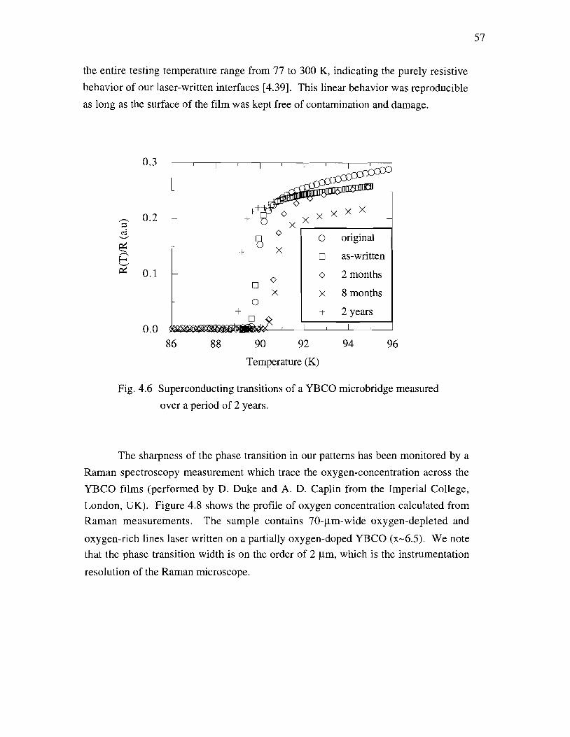
the entire testing temperature range from 77 to 300 K, indicating the purely resistive
behavior of our laser-written interfaces [4.39]. This linear behavior was reproducible
as long as the surface of the film was kept free of contamination and damage.
I o 2 months I 7 0
x 8 months
86 8 8 90 92 94 96
Temperature (K)
Fig. 4.6 Superconducting transitions of a YBCO microbridge measured
over a period of 2 years.
The sharpness of the phase transition in our patterns has been monitored by a
Raman spectroscopy measurement which trace the oxygen-concentration across the
YBCO films (performed by D. Duke and A. D. Caplin from the Imperial College,
London, UK). Figure 4.8 shows the profile of oxygen concentration calculated from
Raman measurements. The sample contains 70-pm-wide oxygen-depleted and
oxygen-rich lines laser written on a partially oxygen-doped YBCO (x-6.5). We note
that the phase transition width is on the order of 2 pm, which is the instrumentation
resol~ution of the Raman microscope.

-30 -20 -10 0 10 20 30
Voltage (mv)
Fig. 4.7 A family of I-V characteristics of a 10-pm-long oxygen-poor YBCO
structure. The inset shows the configuration of our test structure.
0.0 0 100 200 300
Posltlon on sample
Fig. 4.8 Oxygen concentration profile across laser-written YBCO
structures with three different oxygen contents.

4.5.5 Patterning of YBCOlSrTi03 bilayers
To test the ability of laser writing to pattern multilayer YBCO Ttructures, we
investigated the patterning of YBCO/SrTi03 bilayers. 150-nm-thick YBCO thin
films sputtered on LaA103 or SrTi03 substrates were protected with in-situ grown
100-nm-thick SrTi03 cap layers [4.1 I]. The YBCOlSrTi03 bilayers were
deox:ygenated by furnace annealing at 700 OC for 1-2 hours in an Ar atmosphere.
Laser writing has successfully recovered the superconducting properties of the
YBCO films beneath the SrTi03 top layer. Figure 4.9 demonstrates the oxygen-rich
(dark) and oxygen-depleted (bright) patterns fabricated by controlling the oxygen in-
or out-diffusion through the SrTi03 top layer. The background is a partially
oxyg~mated YBCO.
Fig. 4.5) Laser-written patterns fabricated on YBCO/SrTi03 bilayers: (a)
two 35-pm-wide superconducting lines (dark region) cut by a
perpendicular oxygen-depleted line (bright); and (b) part of a
SuFET structure [4.44].

4.6 Device fabrication and characterization
4.6.1 Microwave components
To test the performance of the laser written structures, a number of microwave
and optoelectronic circuits have been designed and fabricated. For microwave
testing, a superconducting coplanar strip (CPS) transmission line and an open-ended
superconducting CPS resonator were fabricated on an insulating YBCO film using
laser writing. Figure 4.10 shows the optical micrograph of part of the CPS
transmission line and resonator. In the CPS resonator, tht: 10-pm-wide oxygen-poor
coupling slots were patterned by erasing in N2 the previously written oxygen-rich
line. Microwave testing of the above structures was performed at Prof. Don Butler's
group at the Southern Methodist University. For the open-ended resonator, the
unloaded Q-factor measured at 24 K was about 5000 at 6.05 GHz [4.40]. At
temperature above Tc (100 K), the unloaded Q-factor was measured to be
approximately unity.
Figure 4.11 displays the measured S2l parameter of the CPS transmission line
as a function of frequency. At room temperature, the line exhibits a lossy attenuation
as the structure consists of parallel metallic YBa2Cu307 and semiconducting
YBa:!Cu306 regions. As the temperature drops, the conductivity of the YBa2Cu307
strips linearly increases and the resistivity of the YBa2Cu3'36 area increases according
to the Mott's VRH. The attenuation decreases as a result of reduced series and shunt
loses. At temperatures below Tc, the CPS strips become superconducting and the
YBqlCu306 region is almost insulating. The S21 parameter is near 0 dB for all the
temperatures below Tc, indicating low microwave losses of our CPS transmission
line.

Fig. 4.. 10 Optical micrograph of part of (a) a micrclwave resonator, and
(b) a coplanar waveguide.
0 5 10 15 Frequency (GHz)
Fig. 4.. 11 Transmitted power S2] versus frequencj7 for a laser written
coplanar transmission line from room temperature to 24 K.

4.6.2 Photoconductive switch
Figure 4.13 shows a test structure of a photoconductive switch based on
oxygen-depleted YBCO and incorporated into a superconducting coplanar
transmission line. The superconducting strips as well as the semiconducting switch
were patterned by the laser-writing technique. An interdigitated finger geometry with
4 prni spacing was implemented in the switch design to enhance the signal gain. The
incident excitation beam came from a Ti:sapphire laser and was modulated by an
acou:stic-optic crystal. The beam was then focused on the switch structure to excite
free carriers.
The frequency response of this photoconductive switch is shown in Fig. 4.14.
Due .to a slow response time of the oscilloscope used in these experiments, we did not
observe the direct response from individual femtosecond pulses generated by the
Ti:sapphire laser. Instead, the photo-induced voltage pulses followed the acoustic-
optical crystal. modulation frequency. Frequencies above 3 MHz already exceed the
bandwidth of the oscilloscope (1 MHz). Therefore, the roll-off in Fig. 4.13 is
cons-idered a result of the narrow bandwidth of the oscilloscope. The lifetime of
semi~conducti~ig YBCO can be estimated as shorter than 300 ns, a value comparable
with that obtained by other groups [4.4-1-4.431.
The results presented in Fig. 4.14 were obtained at room temperature.
However, low temperature measurements displayed a similar behavior. No
significant effect of persistent photodoping has been observed at our excitation level
(1 m'W beam power, 40 pm in diameter).

Excitation beam
Output dc
Bias
I Oxygen-depleted YBCO
Fig. 4.12 Semiconducting YBCO photoconductive switch: experimental set-up.
1 o4 lo5 1 o6 1 o7 Frequency (Hz)
Fig. 4..13 Room temperature response of an oxygen-depleted YBCO photoconductive switch with 4-pm spacing. Bias at 25.6 V.
4.7 Summary
We have developed a laser-writing technique which is proven to be a practical
and reliable method of patterning YBCO thin-film devices and circuits. The method
results in planar structures with well-defined lines and undamaged crystalline
structure. The superconducting properties of our oxygen-rich patterns are found to be
as good as that of the original films. At the same time, the patterned oxygen-depleted
regions are practically insulating at low temperatures. The nondestructive nature of
laser writing makes it the only existing way of combining superconducting and
semiconducting YBCO regions in the same film. The ability of erasing previously
patterned structures is also extremely convenient for circuit restructuring and fault
correction. Laser writing is capable of patterning through a top SrTi03 layer. Our
test structures are shown to exhibit long-term stability. Furthermore, the method is
free of photomasks and chemicals. And that prevents contamination of the film
surface. In terms of cost, the technique does not require any vacuum equipment
and/or pumps.
Various structures, such as microwave resonators, CPS transmission lines,
field-effect devices [4.44] and photoconductive switches were successively fabricated
using this method. We believe that laser writing will continue to play an important
role in the new HTS electrical and optoelectronic applications.

References
Conventional Patterning
[4.1] See, e.g., A. I. Braginski, Springer Proceedings in Physics, vol. 64, H. Koch
and H. Liibbig, eds., Springer-Verlag, Berlin, Heidelberg, (1992).
[4.2] J. S. Martens, T. E. Zipperian, D. S. Ginley, V. M. Hietala, C. P. Tigges, and
T. A. Plut, "The effects of processing sequences on the microwave surface
resistance of TlCaBaCu0,"J. Appl. Phys. 69, 8268 (1991)
Laser Writing
[4.3] M. Rothschild, J. H. C. Sedlacek, J. G. Black, and D. J. Ehrlich, "Laser
patterning of Metal oxide superconductor films by reactive solid-state
transformation," IEEE Electron Device Lett. 9 ,68 (1988)
l4.4-] M. Rothchild, J. H. C. Sedlacek, J. G. Black, and D. J. Ehrlich, "Reversible
laser chemically induced phase transformations in thin-film Ba2YCu30,
superconductors," Appl. Phys. Lett. 52, 404, (1988)
[4.5] R. R. Krchnavek, S. W. Chan, C. T. Rogers, F. De Rosa, M. K. Kelly, P. F.
Miceli, and S. J. Allen, "Transport in reversibly laser-modified YBa2Cu307-,
superconducting thin films," J. Appl. Phys. 65, 1802, (1989)
[4.6] R. C. Dye, R. E. Muenchausen, N. S. Nogar, A. Mukherjee, and S. R. J.
Brueck, "Laser writing of superconducting patterns on YBa2Cu30x films,"
Appl. Phys. Lett. 57, 1149 (1990).
[4.7] Y. Q. Shen, T. Freltoft, and P. Vase, "Laser writing and rewriting on
YBa2Cu307 films," Appl.Phys.Lett. 59, 1365 (1991).
[4.8] R. Sobolewski, W. Xiong, and W. Kula, "Patterning of thin-film high-T,
circuits by the laser-writing method," IEEE Trans. Appl. Supercon. 3, 2896
(1 993)
[4.9] R. Sobolewski, W. Xiong, W. Kula, and J. R. Gavaler, "Laser patterning of Y-
Ba-Cu-O thin-film devices and circuits," Appl. Phys. Lett. 64, 643 (1994)
[4.10] W. Xiong, W. Kula, and R. Sobolewski, "Fabrication of High-T,
superconducting electronic devices using the laser-writing technique," in
Advances in Cryogenic Engineering, 40, p. 385, edited by R. P. Reed et al.,
(Plenum Press, 1994).
[4.11] W. Kula, W. Xiong, and R. Sobolewski, "Laser patterning of YBa2Cu30x thin
films protected by in-situ grown SrTi03 cap layer," IEEE Trans. Appl.
Supercond. 5, 1 177 (1 995)

Oxygen Dependence
[4.12] J. D. Jorgensen, B. W. Veal, A. P. Paulikas, L. J. Nowicki, G. W. Crabtree, H.
Claus, and W.K. Kwok, "Structural properties of oxygen-deficient
YBa2Cu307-6 ," Phys. Rev. B 41, 1863 (1990)
[4.13] E. Osquiguil, M. Maenhoudt, B. Wuyts, and Y. Bruynseraede, "Controlled
preparation of oxygen deficient YBa2Cu30, films," Appl. Phys. Lett. 60,
1627 (1992)
Laser Direct Writing in VLSI
[4.14] D. J. Ehrlich, and J. Y. Tsao, in VLSI Electronics: Microstructure Science,
vol. 7, p. 129, ed. N. G. Einspruch, Academic Press (1983)
[4.15] D. J. Ehrlich and J. Y. Tsao, "Submicrometer-linewidth doping and relief
definition in silicon by laser-controlled diffusion," Appl. Phys. Lett. 41, 297
(1982)
[4.16] D. J. Ehrlich, R. M. Osgood Jr., and T. F. Deutsch, "Laser chemical technique
for rapid direct writing of surface relief in silicon," Appl. Phys. Lett. 38, 1018
(1981)
[4.17] D. J. Ehrlich, R. M. Osgood Jr., and T. F. Deutsch, "Laser microreaction for
deposition of doped silicon films," Appl. Phys. Lett. 39, 957 (1981)
Oxygen Diffusion in YBCO
[4.18] J. Park, P. Kostic, and J. P. Singh, "Electrical conductivity and chemical
diffusion in sintered YBa2Cu30y," Mater. Lett. 6, 393 (1988)
[4.19] K. N. Tu, S. I. Park, and C. C. Tsuei, "Diffusion of oxygen in superconducting
YBa2Cu307-6 oxide upon annealing in helium and oxygen ambients," Appl.
Phys. Lett. 51,2158 (1988)
[4.20] K. N. Tu, N. C. Yeh, S. I. Park, and C. C. Tsuei, "Diffusion of oxygen in
superconducting YBa2Cu307-6 ceramic oxides," Phys. Rev. B 39, 304 (1989)
[4.21] X. M. Xie, T. G. Chen, and Z. L. Wu, "Oxygen diffusion in the
superconducting YBa2C~307-~," Phys. Rev. B 40,4549 (1989)
[4.22] S. J. Rothman, J. L. Routbort, and J. E. Baker, "Tracer diffusion of oxygen in
YBa2Cu307-6," Phys. Rev. B 40, 8852 (1989)
[4.23] B. W. Veal, H. You, A. P. Paulikas, H. Shi, Y. Fang, and J. W. Downey,
"Time-dependent superconducting behavior of oxygen-deficient YBa2Cu30,:
possible annealing of oxygen vacancies at 300 K," Phys. Rev. B 42, 4770
(1 990)

[4.24] J. L. Tallon and M. P. Staines, "Oxygen self-diffusion coefficient in the
superconductor YBa2Cu307-6 from internal friction measurements," J. Appl.
Phys. 68,3998 (1990)
[4.25] J. R. LaGraff, P. D. Han, and D. A. Payne, "Resistance measurements and
oxygen out-diffusion near the orthorhombic-tetragonal phase transformation
in single-crystal YBa2Cu307-6,"Phys. Rev. B 43,441 (1991)
[4.26] Y. Chen, J. Zhang, Z. Wu, "Oxygen diffusion in c-axis-oriented YBa2Cu30,
films," Supercond. Sci. Technol. 5,463, 1992
[4.27] J. R. LaGraff, P. D. Han, and D. A. Payne, "Oxygen in-diffusion and out-
diffusion in single crystal YBa2Cu307-6," in Defects in Materials, e d ~ . P. D.
Bristowe, J. E. Epperson, J. E. Griffith, and Z. Liliental-Weber, Mat. Res. Soc.
Symp. Proc. 209,801 (1991)
In situ Oxygenation
[4.28] E. S. Hellman, D. G. Schlom, N. Missert, K. Char, J. S. Harris, M. R. Beasley,
A. Kapitulnik, T. H. Geballe, J. N. Eckstein, S. L. Weng, and C. Webb,
"Molecular-beam epitaxy and deposition of hig-T, superconductors," J. Vac.
Sci. Technol. B 6,799 (1989)
[4.29] N. Missert, R. Hammond, J. E. Mooj, V. Matijasevic, P. Rosenthal, T. H.
Geballe, A. Kapitulnik, M. R. Beasley, S. S. Laderman, C. Liu, E. Garwin,
and R. Barton, "In situ growth of superconducting YBaCuO using reactive
electron-beam coevaporation," IEEE Trans. Magn. MAG-25, 2418 (1989)
[4.30] T. Goto, H. Matsunoto, T. Hirai, "Preparation of superconducting
YBa2Cu307-, films by ECR plasma sputtering," Jpn. J. Appl. Phys. 28, L88
(1989)
[4.31] R. M. Silver, A. B. Berezin, M. Wendman and A. L. de Lozanne, "As-
deposited superconducting Y-Ba-Cu-0 thin films on Si, A1203, and SrTi03
substrates," Appl. Phys. Lett. 52, 2174 (1988)
[4.32] T. Terashima, Y. Bando, K. Iijima, K. Yamamoto, and K. Hirata, "Epitaxial
growth of YBa2Cu307-x thin films on (110) SrTi03 single crystals by
activated evaporation," Appl. Phys. Lett. 53,2232 (1988)
[4.33] X. D. Wu, A. Inam, T. Venkastesan, C. C. Chang, E. W. Chase, P. Barboux, J.
M. Tarascon, and B. Wilkens, "Low-temperature preparation of high Tc
superconducting thin films," Appl. Phys. Lett. 52,754 (1988)
[4.34] Z. P. Zheng, Q. Y. Ying, S. Witanachchi, Z. Q. Huang, D. T. Shaw, and H. S.
Kwok, "***," Appl. Phys. Lett. 54,954 (1989)

[4.35] G. Koren, A. Gupta, and R. J. Baseman, "Role of atomic oxygen in the low-
temperature growth of YBa2Cu307-6 thin films by laser ablation," Appl. Phys.
Lett. 54, 1920 (1989)
Oxygen Ordering [4.36] B. W. Veal, A. P. Paulikas, H. You, H. Shi, Y. Fang, and J. D. Downey,
"Observation of temperature-dependent site disorder in YBa2Cu307-6 below
150 OC," Phys. Rev. B 42,6305 (1990)
[4.37] G. Nieva, E. Osquiguil, J. Guimpel, M. Maenhoudt, B. Wuyts, Y.
Bruynseraede, M. B. Maple, and I. K. Schuller, "Photoinduced enhancement
of superconductivity," Appl. Phys. Lett. 60,2159 (1992)
Semiconducting/Superconducting Interface
[4.38] C. M. Ray, H. Mathias, L. R. Testardi, and S. Skirius, "High dielectric
constant and nonlinear electric response in nonmetallic YBa2Cu306+6," Phys.
Rev. B 45, 10639 (1992)
[4.39] R. Sobolewski, W. Xiong, W. Kula, and B. McIntyre, "Electrical and
structural properties of the YBCO superconducting-semiconducting
interface," Physica B 194-196,2143 (1994)
Microwave Testing
[4.40] W. N. Maung, D. P. Butler, W. Xiong, W. Kula, and R. Sobolewski,
"Propagation characteristics of monolithic YBaCuO coplanar strip
transmission lines fabricated by laser-writing patterning technique," IEEE
Microwave and Guided Wave Lett. 4, 132 (1994)
Lifetime of Photoexcited Carriers
[4.41] G. Yu, A. J. Heeger, G. Stucky, N. Herron, and E. M. McCarron, L. Cong, G.
C. Spalding, C. A. Nordman, and A. M. Goldman, "Phase separation of
photogenerated carriers and photoinduced superconductivity in high-T,
materials," Phys. Rev. B 45,4964 (1992)
[4.42] F. A. Hegmann, J. S. Preston, "Origin of the fast photoresponse of epitaxial
YBa2Cu307-6 thin films," Phys. Rev. B 48, 16023 (1993)
[4.43] M. Johnson, "Nonbolometric photoresponse of YBa2Cu307-6 films," Appl.
Phys. Lett. 59, 1371 (1991)
FET Structure [4.44] W. Kula and R. Sobolewski, "Charging effect in partially oxygen-depleted
superconducting Y-Ba-Cu-0 thin films," Phys. Rev. B 49, 6428 (1994)

5 FEMTOSECOND OPTICAL RESPONSE
5.1 Introduction
In this Chapter, we investigate the nonequilibrium optical response by a
femotosecond pump-probe technique. We first give a brief review of the sources and
models of pump-probe signals. Then we study the relaxation of photoexitation in
YBCO thin films containing several different oxygen contents. The experiments
performed in this Chapter are trying to explain the origins of the optical response in
YBCO and to depict the material's band structure.
5.1.1 Pump-probe technique
With the advance of femtosecond laser pulses [5.1-5.41, femtosecond
spectroscopy has emerged as a powerful tool for the investigation of transient
nonequilibrium processes in solid state materials [5.5-5.301. Due to the difference in
the heat capacities between the electrons and lattice, it is possible to excite by
femtosecond lasers a non-equilibrium distribution of electrons with temperatures
much higher than that of the lattice. The hot carriers then lose their energy by
scattering with carriers, LO phonons, and acoustic phonons. Hence, femtosecond-
resolved relaxation of photo-excited carriers contains valuable information about e-ph
coupling strength and other carrier dynamics.
Standard pump-probe experiments measure the difference in reflection and
transmission before and after pulsed-laser excitation. In case of a non-degenerate
two-band semiconductor, the band filling term of the observed difference in
absorption can be expressed as
where fc and fv are the probability of electron occupancy in the conduction and
valence bands after photoinjection, respectively, and a0 is the linear absorption
coefficient for interband transition. Therefore, bandfilling results in PB signals.
For small changes in optical constants, the normalized differential reflectivity
AWR can be expressed as

where E 1 and ~ 2 are the real and imaginary parts of the dielectric constant.
Any change in the electron distribution will affect the interband transition
which is directly related to ~ 2 . Hence, electron temperature rise by laser heating is
expected to generate AFUR with a sign determined by the probe energy.
Besides the PB from the band filing, PA is also possible to contribute to the
differential signals. Sources for induced absorption include intra-band free-carrier
absorption, excitation of carriers trapped in localized states, and nonlinear two-photon
absorption. Among them, transition from localized states has the biggest transition
cross section because it is a dipole-allowed first-order process.
Band renormalization or bandgap shrinkage are significant contributions for
bandedge excitation of small-gap semiconductors. However, the effect of band
renormalization is negligible in our study because of the large CT gap (- 1.7 eV) of
the semiconducting YBCO and the pump energy ( 2 eV) far above the band edge. For superconductors, the optical conductivity o is written in term of the two
fluid model as
where Nn and Ns are the relative density of the normal (Drude) and the
superconducting electrons, on and os are their respective optical conductivities.
The generation of QP leads to an increase in Nn at the expense of Ns. The
change in dielectric constants is then expressed as [5.16,5.24]
where 8NqP is the fraction of photogenerated QP, op is the plasma frequency, 112 is
the scattering rate of Drude carriers. According to Eq. (5.2), QP generation caused change in A E ~ and A E ~ will
result in a change of transient reflectivity.
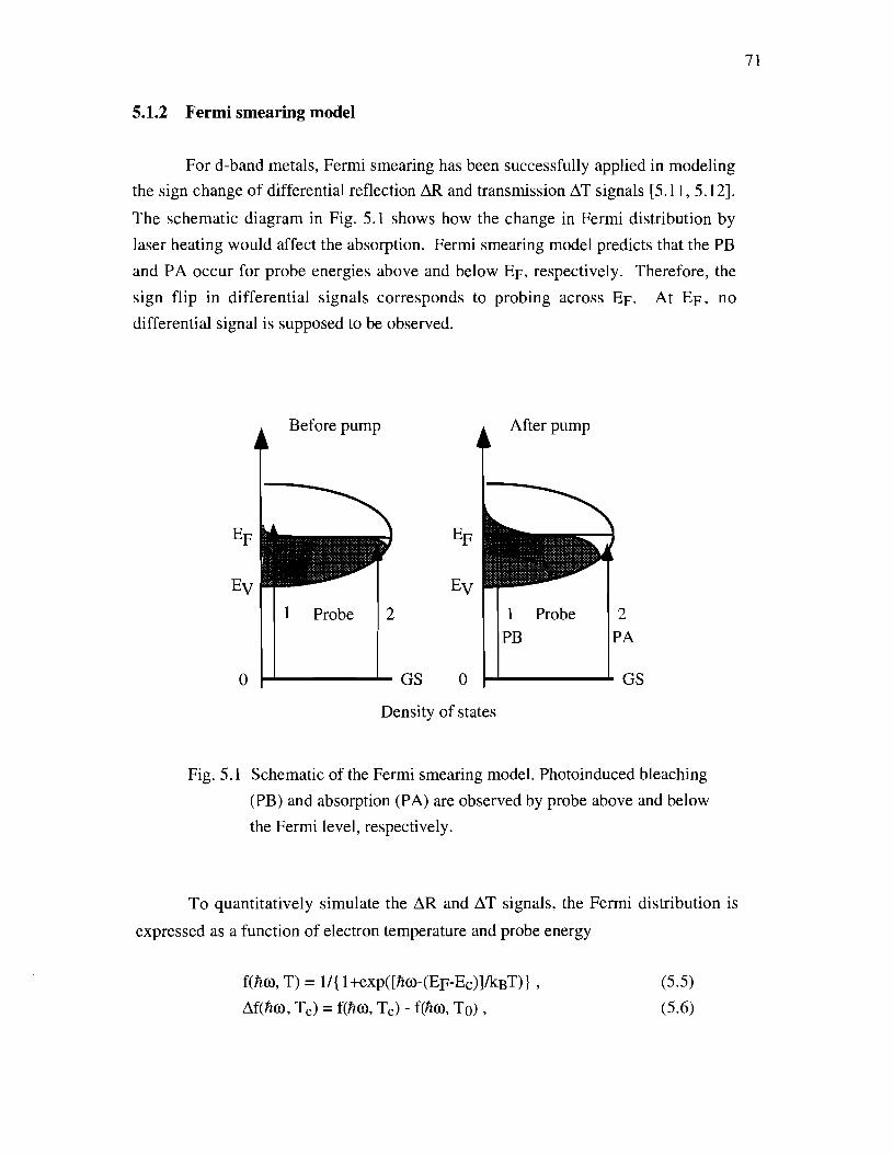
5.1.2 Fermi smearing model
For d-band metals, Fermi smearing has been successfully applied in modeling
the sign change of differential reflection AR and transmission AT signals [5.11, 5.121.
The schematic diagram in Fig. 5.1 shows how the change in Fermi distribution by
laser heating would affect the absorption. Fermi smearing model predicts that the PB
and PA occur for probe energies above and below EF, respectively. Therefore, the
sign flip in differential signals corresponds to probing across EF. At EF, no
differential signal is supposed to be observed.
EF EF
E v EV
0 GS 0
Density of states
Fig. 5.1 Schematic of the Fermi smearing model. Photoinduced bleaching
(PB) and absorption (PA) are observed by probe above and below
the Fermi level, respectively.
To quantitatively simulate the AR and AT signals, the Fermi distribution is
expressed as a function of electron temperature and probe energy
f(ho, T) = l/{ l+exp([ho-(EF-E~)]/~BT)] ,
Af(ho, T,) = f(ho, T,) - f(h0, To) ,

where Ec is the separation between the ground state and the conduction band, To and
T, are the electron temperatures before and after the pump excitation, respectively,
and Ao the photon energy.
Figure 5.2 shows a sign flip in the distribution function when probe energy
crosses the Fermi level. According to Fermi smearing model, no sign change can be
produced by changing the pump intensity alone.
-0.6 -0.4 -0.2 0 0.2 0.4 0.6 Energy (eV)
Fig. 5.2 Ferrni smearing of differential signals. Energy zero is set
to be EF-E,.

5.1.3 Nonequilibrium electron heating
The heat generated by the pump pulse is also subjected to diffuse out of the
excited area. However, due to the short (ps) measurement window of our
experiments, the slow thermal diffusion process can be neglected. Therefore, the
temporal profiles of the electron and lattice temperatures Te and TL can be modeled
as [5.21, 5.291
where Ce*, is the electronic specific heat, CL=C(Tr/O)3 is the lattice specific heat,
O is the Debye temperature, g=3hxyh<02>l.nkB is the coupling constant, and h<02>
is the e-ph coupling constant.
According to the above equations, an initial fast decay in differential signals is
expected, as the electron temperature drops quickly by e-ph coupling. After thermal
equilibrium is reached among the electron and lattice systems, a slow bolometric
component is predicted to represent the heat diffusion process.
From Eqs. (5.7a) and (5.7b), the electron temperature can be expressed by the
following nonlinear differential equation:
where the variables are the electron temperatures and the e-ph coupling constant.
Transient reflectivity can be also expressed as
For given boundary conditions Te(0) and Te(m), time-resolved ARIR can be
numerically fitted by adjusting the e-ph coupling constant h<o2> in Eq. (5.8). As a
result, the strength of the e-ph coupling is obtained from the pump-probe results.

5.2 Experimental
Optical density of YBCO films was measured using a Perkin-Elmer Lambda-9
spectrometer. The femtosecond pump-probe response was investigated in the
temperature range between room temperature and 12 K. Figure 5.3 shows the
experimental set-up of our pump-probe system. Laser pulses of 120 fs in duration
were generated by a colliding-pulse-mode-locked laser and further amplified by a
copper vapor laser at a repetition rate of 8.5 KHz. While the pump energy was fixed
at 2 eV, variable probe energies were obtained from the white-light continuum. Pump
and probe beams were cross-polarized and focused on the sample surface with a
diameter of 30 pm. With the pump energy of 10 nJ per pulse, the injected carrier
density is estimated to be 3x10²⁰ ~ m - ~ . Lock-in and differential detection techniques
were used to enhance the signal-to-noise ratio. Time-resolved transient changes in
both R and T were measured simultaneously so that the Aa and the unperturbed
absorption coefficient (ao) could be obtained by numerical fitting. Low temperature
measurements were performed in a continuous He-flow optical cryostat using 2 eV
pump and probe pulses.
The measured reflection and transmission can be expressed as functions of the
real (n) and imaginary (k) part of refractive index:
Consequently, values of n, k, and absorption coefficient ( a = 4nklh) can be
converted from the measured T and R by solving numerically Eqs. (5.10) [5.15].
Fabry-Perot effects are included in the fitting program to eliminate the artifact of
interference. Figure 5.4 shows an example conversion of n and k from a set of
measured ARIR and ATIT data in a semiconducting YBCO thin film.
As described in Section 3.4, semiconducting YBCO-on-MgO thin films of
200-nm thick were fabricated using rf magnetron sputtering and in-situ annealing in
100 mTorr of Ar. Oxygen-doped YBCO-on-LaA103 samples of 200-nm thick were
off-axis sputtered and annealed to obtain samples with TC's of 30 K, 55 K, and 60 K,
as well as Tc=90 K.
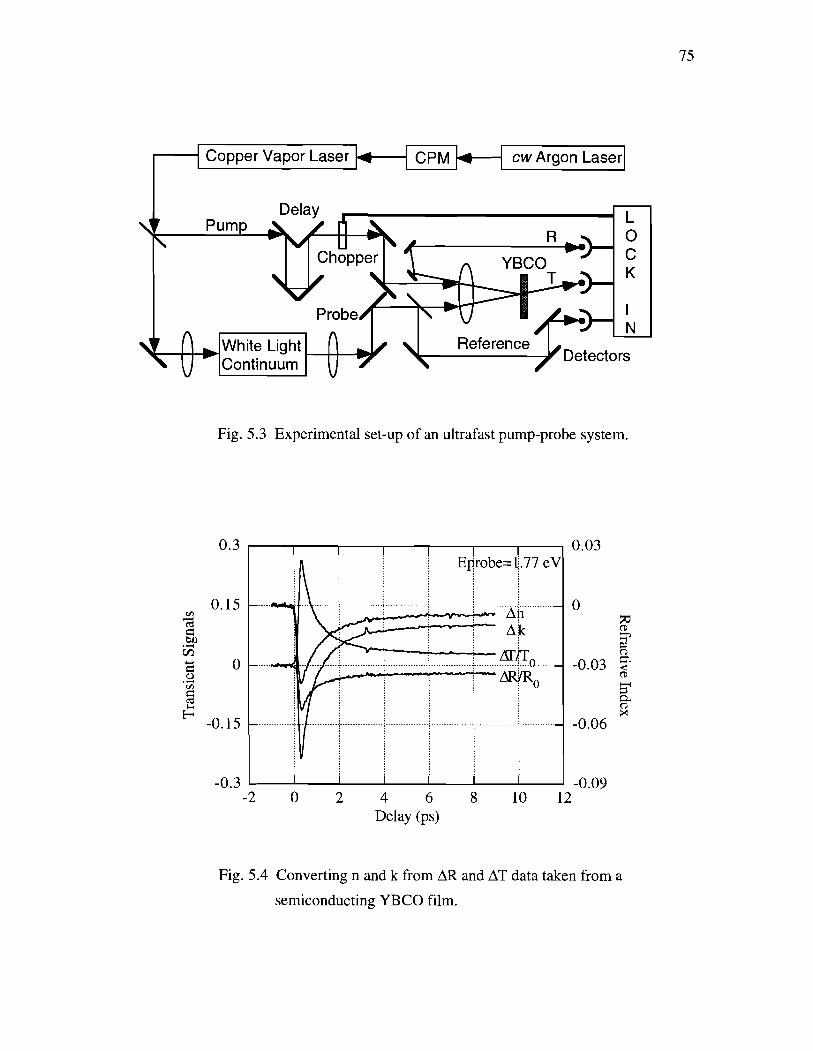
Fig. 5.3 Experimental set-up of an ultrafast pump-probe system.
Copper Vapor Laser
Fig. 5.4 Converting n and k from AR and AT data taken from a
semiconducting YBCO film.
CPM cw Argon Laser

5.3 Results and Discussion
5.3.1 Semiconducting YBCO
Recent femtosecond studies by Matsuda et al. [5.30] have observed both PB
and PA signals in insulating cuprates. The initial subpicosecond decay of the
bleaching was assigned to the emission of two magnons; however, the origin of the
induced absorption below 1.6 eV was not fully understood. As we outlined in
Chapter 2, semiconducting YBa2Cu30, (x<6.3) is considered as a charge-transfer
insulator with a CT gap between the Cu-3d upper Hubbard band and the 0-2p band.
Several corresponding band diagrams have been proposed based on Raman [5.3 1,
5.321, photoconductivity [5.33, 5.341, and photoluminescence [5.35] studies.
Moreover, transient photoconductivity investigation [5.33] as well as our
photoconductive switch measurement (see Sec. 4.6.2) have shown a long lifetime
(>lo ns) for photo-excited carriers in insulating YBCO.
In this Section, we explore the mechanisms of the nonequilibrium optical
response in oxygen-poor semiconducting YBCO by means of femtosecond pump-
probe technique. We investigate the transient response as a function of probe energy
from 1.65 to 2.10 eV and ambient temperature between 12 to 300 K.
Figure 5.5 shows the room temperature linear absorption spectrum of an
oxygen-depleted YBa2Cu30, (x-6.0) film. Two main absorption features near 1.78
and 2.8 eV are clearly resolved. These two peaks are related to the CT transition
between the filled Cu-3d UHB and the empty 0-2p band (in the hole picture) [5.3 1,
5.341 (see also Sec. 2.3). In addition, a broad band tail is observed below the
fundamental absorption peak near 1.78 eV. Low-temperature photoconductivity
studies have indicated that the lowest interband transition occurs at 1.5 eV [5.34].
Therefore, it can be concluded that all probe energies used in the our study (>1.65 eV)
are greater than the CT gap. Thus, bleaching is expected as a result of band filling.
Also shown in Fig. 5.5 are the values of a 0 (dots) obtained from the numerical fitting
of our pump-probe data. The good agreement between our data points and the linear
absorption curve demonstrates the effectiveness of our fitting program.
Figure 5.6 displays the normalized transient absorption at probe energies from
1.65 to 2.1 eV. As expected, bleaching (Aa<O) is observed at all wavelengths
immediately after the excitation. The pulse width-limited rise of the bleaching is due
to the efficient redistribution of photo-excited carriers by carrier-carrier (CC)
scattering. As in the case of conventional semiconductors such as GaAs [5.7], CC

scattering occurs on a sub-100 fs time scale when the injected carrier density is higher
than 1019 cm-3. The redistributed carriers, which now occupy the previously empty
states, block the possible transitions across the CT gap.
0 0 1 2 3 4 5 6 7 8
Photon Energy (eV)
I I I I I I I
YBa2Cu306.0
Fig. 5.5 Linear absorption spectrum of semiconducting YBCO. Solid
-
dots in the inset are obtained from our pump-probe measurements.
-
The excess energy of the excited carriers is then transferred to the lattice.
Since the carrier lifetime (>lo ns) is much longer than our 10-ps measurement
window, one would expect carrier accumulation near the band edge prior to
recombination. As a consequence, for photon energies near the band edge, the
recovery of bleaching should become a slow process. In some cases, the bleaching
could even increase with time as the carriers cool down to near room temperature.
Instead, we observe that recovery is slowest near 1.9 eV (650 nm), rather than near
the band edge (1.65 eV or 750 nm). Close to the band edge, the bleaching disappears
in a few picoseconds. Further, the signal even becomes positive after 5 ps (Fig. 5.6),
indicating induced absorption. The appearance of induced absorption at 1.65 eV
suggests that the photoinjected carriers can be further excited.
Pump-probe data
-
1.6 1.8 2.0 2.2 I I I I I I I

Fig. 5.6 Differential absorption of semiconducting YBCO at several probe
energies. The smooth lines are stretched-exponential fits.
The relaxation measured by the recovery of the bleaching in Fig. 5.6 cannot be
fitted by a simple exponential function. Instead, it follows a stretched exponential.
The smooth solid lines in Fig. 5.6 are the fits produced by a stretched exponential plus
a constant terrn
Aala = c lexp(-(tl~)P] + C2. (5.10)

While the stretched term models the relaxation of hot carriers, the constant term
represents the excess heat that escapes by the much slower process of heat diffusion
(bolometric process). The fits provide essentially constant values for z = 0.6 ps and P =: 0.7 over the whole investigated spectral range at room temperature. The stretched
exponential decay indicates the co-existence of multiple processes that cannot be
represented by a unique time constant [5.36, 5.371.
Stretched-exponential decay has been considered as a universal law in
describing any dispersive systems [5.36]. For a system at equilibrium, any deviation
(A) from the equilibrium can be expressed as [5.37]
In case of a constant rate v, the decay follows a simple exponential relation
A=Aoexp(-vt). However, if there coexist many time scales, a stretched-exponential
decay is expected
where z is a time constant, p is the dispersive factor and O<P<l.
The stretched exponential is well understood in the case of multiple trapping.
Given a distribution of localized states such as exp(-Elk~To), it has been found that
both z and P are temperature dependent [5.36, 5.371
To test the above model, we performed low-temperature measurements.
Figure 5.7 shows time-resolved AT/T as a function of temperature. The recovery of
ATIT is slightly faster at lower temperatures. As in Fig. 5.6, the relaxation process
can be accurately fitted by a stretched-exponential (the smooth solid lines in Fig. 5.7). Figure 5.8 plots the time constant z and dispersion factor P obtained from the
stretched-exponential fitting in Fig 5.7 as a function of temperature. Unlike in the
case of multiple trapping where P=T/To, our value of P is independent of temperature.
Moreover, the time constant z cannot be fitted by a thermally activated exponential.
Instead, it decreases with decreasing temperature. Therefore, our results cannot be
explained by the multiple trapping. We believe that the increase in decay rate at low
temperature may be related to the emission of acoustic phonons.

Fig. 5.7 ATIT of semiconducting YBCO at several temperatures. Fitting
using ATIT = ~ ~ e x ~ [ - ( t l ~ ) P ] + C2 is shown in solid smooth lines.
0 50 100 150 200 250 300
Temperature (K)
Fig. 5.8 Stretched-exponential parameters for the data from Fig. 5.8.
Solid lines are guides to the eye.

In Fig. 5.9, the transient absorption spectra from Fig. 5.6 are plotted for
different delays. The maximum bleaching occurs at -320 fs, consistent with the
pulse-width limited rise time and fast CC scattering. Moreover, the maximum
bleaching is at 1.9 eV, an energy at which no spectral peak in the linear absorption is
observed. There is no observable spectral shift of the 1.9-eV peak with time over a 10
ps window. The decay in Fig. 5.9 shows clearly that the slowest recovery occurs near
1.9 eV instead of at the band edge. The small increase in absorption at 1.65 eV after
5 ps indicates that induced absorption overcomes bleaching. From the injected carrier
density of about 3x10²⁰ ~ m - ~ and the magnitude of induced absorption (-300 cm-I),
we deduce a transition cross section of about 3x10-18 cm2. Due to the partial
cancellation of the induced absorption by bleaching, the real transition cross-section
for free-carrier absorption could be larger than this. Nevertheless, the above value is
consistent with free-carrier absorption involving extended states and is much smaller
than the dipole-allowed transitions from carriers trapped in the localized states.
Therefore, the most likely bleaching cancellation process is the free-carrier absorption
inside the 0-2p band.
1.6 1.7 1.8 I .9 2 2.1 2.2
Probe Energy (eV)
Fig. 5.9 Differential absorption spectrum at several delays after
the maximum bleaching.

Free-carrier absorption inside the 0-2p band depends strongly on the probe
energy. At probe energy larger than the band width of 0-2p band, no intraband
transition is available and only bleaching exists. Below that threshold energy,
however, induced absorption and bleaching coexist and cancel with each other. The
net result is an increase of the recovery rate of the bleaching and eventually induced
absorption. Consequently, the fact that the fastest recovery occurs near 1.9 eV
corresponds to the threshold for free-carrier absorption. The recovery peak near 1.9
eV should be related to the bandwidth of the 0-2p band. For smaller probe energies,
the induced absorption is stronger because more occupied states are available for
intraband transitions. As a result, the recovery rate of the differential signals
increases drastically towards the band edge.
5.3.2 YBCO thin film with T,=30 K
As discussed in detail in Chapter 2, oxygen doping of semiconducting YBCO
results in a 0 - T phase transition. The corresponding electronic structure changes
from semiconducting to metallic at room temperature. The filling of chain O(1) sites
removes electrons from the CuO2 plane and creates free holes in the conduction band.
As in other d-band metals, Fermi smearing is expected to contribute to the differential
signal in the metallic YBCO.
Figure 5.10 plots the optical density of a YBCO thin film with T,=30 K.
Comparing with that of semiconducting YBCO (Fig. 5.5), the CT peak near 1.8 eV
drops significantly, but it is still visible. Simultaneously, free-carrier absorption term
increases drastically at low energies.
Transient ARIR of a 30-K YBCO sample is shown in Fig. 5.1 1. Bleaching
signals are observed for all three probe energies. The sources of the bleaching could
be either the Fermi smearing or the band filling across the CT gap. However, due to
the low oxygen doping, the Fermi level is expected to lie far below our probe
energies. Thus, the bleaching is most likely the consequence of band filling.
Figure 5.12 demonstrates the intensity dependence of the bleaching probed at
1.91 eV. The inset shows a linear relation between the maximum bleaching and
pump intensity. This fact further supports that band filling is the origin of bleaching
in our 30-K YBCO sample.

0 0 1 2 3 4 5 6 7
Photon Energy (eV)
Fig. 5.10 Linear absorption spectrum of YBCO with Tc=30 K.
I I I I I
Probe energy = 2.07 eV
0 1 2 3 4 5 6 Time (ps)
Fig. 5.1 1 Transient reflection of YBCO with Tc=30 K.

-20 - 1 0 1 2 3 4 5 6
Time (ps)
Fig. 5.12 Pump intensity dependence of a Tc=30 K YBCO thin film.
Maximum intensity I0=300 p ~ l c m ~ . Probe at 1.9 1 eV.
5.3.3 YBCO thin film with T,=60 K
Further oxygen doping continues to raise the Tc until a plateau is reached near
60 K. Figure 5.13 presents the optical density for a YBCO thin film with Tc-60 K.
While the free-carrier absorption keeps increasing at the low-energy end, the CT
feature below 2 eV becomes hardly distinguishable.
White-light investigation of AR/R in a Tc=55 K YBCO thin film is displayed
in Fig. 5.14. Both positive and negative signals are observed in the fast components.
In terms of the Fermi smearing model, the sign flip between 2.07 and 2.10 eV would
be an indication of probing across the Fermi level. After the fast peak, the slow tail
surprisingly increases with time instead of following a bolometric decay.

O I I I I I I I
0 1 2 3 4 5 6 7 Photon Energy (eV)
Fig. 5.13 Linear absorption spectrum of YBCO with T,=60 K.
Fig. 5.14 ARIR of a YBCO film with T,=55 K. Pump at 300 pJIcm2.
15
10
5
0
Probe energy
- (eV> - 1.91
- -
2.00 - -
2.07 - 2.10 -

Figure 5.15 illustrates another white-light response of the 55-K film but with a
much lower pump intensity. This time, the sign flip occurs between 1.65 and 1.72
eV. This value is about 0.4 eV lower than that of high intensity case. Hence, the
energy level for sign flip appears to be dependent on the pump intensity. Such an
observation cannot be explained by the standard Fermi smearing model (see Sec.
5.1.2). If the bleaching at low intensity corresponds to probe energy (1.91 eV) above
the Fermi level, the increase of pump intensity would only enhance the bleaching
(Fig. 5.2). Thus, the intensity dependence might be interpreted as a photoinduced
shift in the F e m i level (photodoping). White-light AFUR signals for a 60-K YBCO sample are presented in Fig. 5.16.
The result is very similar to that of 55-K sample with a sign flip between 2.07 and 2.10 eV. The dependence of AFUR on pump intensity with a 2.0-eV probe is shown in
Fig. 5.17. At high intensities, the fast peak is distinguishable from the slow
component. The ratio between the fast peak and the slow tail drops significantly
towards low pump intensity.
-5 - 1 0 1 2 3 4 5
Time (ps)
Fig. 5.15 ARIR of a YBCO film with T,=55 K. Pump at 75 p/cm2.

-2 - 1 0 I 2 3 4 5
Time (ps)
Fig. 5.16 ARR of a Tc=60 K YBCO thin film. Pump at 160 p.T/cm2.
I I
Probe energy -
1.91 eV -
Fig. 5.17 Pump intensity dependence of a Tc=60 K YBCO thin film.
Maximum intensity I0=300 p~/cm2. Probe at 2 eV.
-
-
-
-
2.00 eV -
2.07 eV - -
2.10 eV - -
I I I I I

The change in ARJR as a function of pump intensity is displayed in Fig. 5.18
for probing at 1.91 eV. Like the 55-K sample, the 60-K film exhibits a strong
intensity dependence of the signal sign. Whereas the negative signal appears at low
intensity, the positive peak occurs at high intensities.
-2 - 1 0 1 2 3 4 5 6 7
Time (ps)
Fig. 5.18 Pump intensity dependence of a T,=60 K YBCO thin film.
Maximum intensity Io= 160 p~Icm2. Probe at 1.9 1 eV.
Possible explanation for the strong intensity dependence seems to be related to
the photodoping effect observed in partially doped YBCO [5.38-5.401. At high
intensities, either the charge-transfer and oxygen-ordering mechanisms proposed for
photodoping could result in an up shift in the Fermi level of the Cu02 plane. As a
consequence, the probe energy which is above the EF at low intensity becomes below
the EF at high intensity. Correspondingly, the sign of the peak signal changes from
negative to positive with increasing pump intensity. Therefore, low intensity result is
believed to reflect more accurately the original position of the Fermi level in our
samples. The observations at low intensity indicate that EF is below 1.9 eV for the
55-K and 60-K samples.

5.3.4 Fully oxygenated YBCO
In oxygen-rich YBCO, the maximum filling of 0 - p band results in a
maximum Fermi energy. Figure 5.19 plots the optical density of a 90-K YBCO thin
film. Below 2 eV, no feature associated with the interband transition across the CT
gap is observed. Only the free-carrier term dominates at the low energy end. Like
other d-band metals 15.11, 5.121, Fermi smearing is expected to govern the
differential signal in this metallic phase of YBCO at room temperature.
0 0 1 2 3 4 5 6 7
Photon Energy (eV)
Fig. 5.19 Linear absorption spectrum of YBCO with T,=90 K.
White-light probed AlUR of an oxygen-rich YBCO is displayed in Fig. 5.20.
Similar profiles with a fast component followed by a long-lasting plateau are
observed for all probe energies. The fast component can be understood as the
efficient cooling of hot electrons through e-ph coupling. The slow term, on the other
hand, can be explained as the bolometric process of phonon diffusion. According to the Fermi smearing model, the positive AlUR peak indicates a Fermi level higher than
the probe energy. Hence, EF of the oxygen-rich sample can be deduced as higher
than 2.18 eV.

Probe Energy
-1 0 4 Delay
Fig. 5.20 Normalized ARIR (-10-3) of an oxygen-rich YBCO thin film.
5.3.5 Nonequilibrium Superconductivity
Cryogenic testing at 2-eV pump and probe energies has been performed to
investigate the recovery of nonequilibrium superconductivity. Figure 5.21 presents ARIR at the temperature of 12 K for (a) a 280-nm thick YBCO film with Tc=89.5 K
and (b) a 80-nm thick YBCO film with Tc=83 K. At low pump intensity (-1 p ~ l c m ~ ) ,
both samples display a fast recovery of ARIR in less than 4 ps. However, the signal
sign of the optically thin sample is opposite to that of the optically thick sample. The
sign reversal between the optically thick and thin samples can be explained by the
thin-film effect [5.25].
Under high-level excitations, the same oxygen-rich YBCO samples behave completely differently. Figure 5.22 displays ARIR for a YBCO sample at two high
excitation levels. At the excitation level of - 20 pJ/cm2, the estimated QP number is
- 1021 cm-3, and is comparable to the total free-carrier concentration in YBCO.
Thus, nearly all of the Cooper pairs are destroyed and the sample undergoes a
superconducting-to-normal transition. The signal in Fig. 5.22(a) shows an instant
thermalization of carriers (initial rise) followed by a fast e-ph coupling decay and a
slow heat diffusion term. In fact, the transient is very similar to that observed at room

temperatures (Fig. 5.20). At the excitation level of -100 pJIcm2, the decay is
dominant by the heat diffusion process [Fig. 5.22(b)].
4 ps .I 2 1 358 Delay
2 1 358
Fig. 5.21 Normalized ARIR (-10-4) at T=25 K of (a) a 280-nm thick YBCO
film with Tc=89.5 K and (b) a 80-nm thick YBCO film with
Tc=83 K. The pump intensity was - 1 pJIcm2.

- 4ps- Delay
Fig. 5.22 Normalized ARIR (-10-3) at T=12 K measured on a 200-nm-thick
YBCO film with T,=87 K. The pump intensity was (a) -20 pJIcm2
and (b) - 100 ~ J l c m ~ .
5.4 Summary
After systematic studies of the transient optical response of YBCO thin films
with various oxygen contents, we obtained valuable information regarding the band
structure as well as the carrier dynamics in this material.
In semiconducting YBCO, a charge-transfer gap has been directly probed.
The fast relaxation below 1.9 eV is attributed to free-carrier absorption inside the
broad 0-2p band. Transient signals in both white-light and low-temperature
measurements follow exactly a stretched-exponential decay rather than a simple
exponential law. Apart from the case of multiple trapping where fl = TITO and T - exp(E,/k~T), the fits of our data show a temperature-independent fl and a
characteristic time T which decreases with temperature. Therefore, our results cannot
be explained by the carriers trapped in localized states. By separating the

contributions from photo-induced bleaching and free-carrier absorption, we
concluded that the peak in the decay rate near 1.9 eV corresponds to the bandwidth of
the 0-2p band.
At low oxygen doping level, the 30-K film displays a PB as a result of band
filling across the CT gap. With further oxygen doping, the 55-K and 60-K samples
show that signal sign depends strongly on the pump intensity. The intensity
dependence of the signal sign is found to be in contrary to the standard Fermi
smearing model. However, it can be explained by Fermi smearing if photodoping is
considered in partially oxygen-depleted samples. Intensity dependence is expected
once EF is shifted by either charge-transfer process in the Cu02 plane or the oxygen
ordering in the CuO chain layers. To minimize the intensity-dependent shift in EF,
low intensity pumping is preferred. Low intensity white-light probing indicates that
the Fermi energy is below 1.91 eV in both the 55-K and 60-K samples.
Room-temperature response in fully oxygenated samples is found to follow
the nonequilibrium electron heating model previously developed for d-band metals.
The fast component corresponds to the energy loss of electrons through e-ph coupling
and the slow term represents the bolometric heat diffusion process. The Fermi level
in the 90-K sample is found to be above 2.18 eV.
At temperatures below Tc, the response of superconducting YBCO depends
drastically on the pump intensity. At low exaction levels (- 1 ~J/cm2), nonbolometric
response is observed, with a sign difference between the optically thin and thick
films. At high excitation levels (>I5 ~ ~ / c r n 2 ) , bolometric response appears as a result
of excess QP generation that destroy the superconductivity. In the latter case, the
response is identical to that observed at room temperature and again can be explained
with the help of nonequibrium electron heating.

References
Femtosecond Lasers
[5.1] R. L. Fork, C. V. Shank, R. Yen, and C. A. Hirlimann, "Femtosecond optical
pulses," IEEE J. Quantum Elec. QE-19,500 (1983)
[5.2] W. H. Knox, M. C. Downer, R. L. Fork, and C. V. Shank, "Amplified
femtosecond optical pulses and continuum generation at 5-kHz repetition
rate," Optics Lett. 9,552 (1984)
[5.3] J. A. Valdmanis, R. L. Fork, and J. P. Gordon, "Generation of optical pulses
as short as 27 femtoseconds directly from a laser balancing self-phase
modulation, group-velocity dispersion, saturable absorption, and saturable
gain," Optics Lett. 10, 13 1 (1985)
[5.4] J. A. Valdmanis and R. L. Fork, "Design considerations for a femtosecond
pulse laser balancing self phase modulation, group velocity dispersion,
saturable absorption, and saturable gain," IEEE J. Quantum Elec. QE-22, 112
(1986)
Pump-Probe on Semiconductors
[5.5] C. V. Shank, R. Yen, and C. Hirliman, "Time-resolved reflectivity
measurements of femtosecond-optical-pulse-induced phase transitions in
silicon," Phys. Rev. Lett. 50,454 (1983)
[5.6] G. C. Cho, W. Kiitt, and H. Kurz, "Subpicosecond time-resolved coherent-
phonon oscillations in GaAs," Phys. Rev. Lett. 65,764 (1990)
[5.7] T. Gong, P. M. Fauchet, J. F. Young, and P. J. Kelly, "Femtosecond gain
dynamics due to initial thermalization of hot carriers injected at 2 eV in
GaAs," Phys. Rev. B 44,6542 (1991)
[5.8] P. M. Fauchet, D. Hulin, R. Vanderhaghen, A. Mourchid, and W. L. Nighan
Jr., "The properties of free carriers in amorphous silicon," J. Non-Crystal.
Solids 141,76 (1992)
[5.9] A. Esser, H. Heesel, H. Kurz, C. Wang, G. N. Parsons, and G. Lucovsky,
"Femtosecond spectroscopic study of ultrafast carrier relaxation in
hydrogenated amorphous silicon a-Si:H," J. Appl. Phys. 73, 1235 (1993)
[5.10] L. H. Acioli, M. Ulman, F. Vallke, and J. G. Fujimoto, "Femtosecond carrier
dynamics in the presence of a cold plasma in GaAs and AlGaAs," Appl. Phys.
Lett. 63,666 (1993)
Pump-Probe on Metals

[5.11] G. L. Eesley, "Generation of nonequilibrium electron and lattice temperatures
in copper by picosecond laser pulses," Phys. Rev. B 33,2144 (1986)
[5.12] R. W. Schoenlein, W. Z. Lin, and J. G. Fujimoto, and G. L. Eesley,
"Femtosecond studies of nonequilibrium electronic processes in metals,"
Phys. Rev. Lett. 58, 1680 (1987)
[5.13] W. S. Fann, R. Storz, H. W. K. Tom, and J. Bokor, "Direct measurement of
nonequilibrium electron-energy distributions in subpicosecond laser-heated
gold films," Phys. Rev. Lett. 68,2834 (1992)
[5.14] C. K. Sun, F. Vallee, L. Acioli, E. P. Ippen, and J. G. Fujimoto, "Femtosecond
investigation of electron thermalization in gold," Phys. Rev. B 48, 12365
(1 993)
Converting of Refractive Index
[5.15] T. Gong, Phd dissertation, Ch. 2, p. 22, EE Dept., Princeton University, 1991
Pump-Probe on HTS
[5.16] S. G. Han, Z. V. Vardeny, 0 . G. Syrnko, and G. Koren, "Femtosecond optical
detection of quasiparticle dynamics in high-T, YBa2Cu3e-6 superconducting
thin films," Phys. Rev. Lett. 65,2708, (1990)
[5.17] G. L. Eesley, J. Heremans, M. S. Meyer, and G. L. Doll, "Relaxation time of
the order parameter in a high-temperature superconductor," Phys. Rev. Lett.
65,3445, (1990)
[5.18] J. M. Chwalek, C. Uher, J. F. Whitaker, and G. A. Mourou, "Femtosecond
optical absorption studies of nonequilibrium electronic processes in high Tc
superconductors," Appl. Phys. Lett. 57, 1696, (1990)
[5.19] W. Albrecht, Th. Kruse, and H. Kurz, "Time-resolved observation of coherent
phonons in superconducting YBa2Cu307-6 thin films," Phys. Rev. Lett. 69,
1451, (1992)
[5.20] S. V. Chekalin, V. M. Farztdinov, V. V. Golovlyov, V. S. Letokhov, Yu. E.
Lozovik, Yu. A. Matveets, and A. G. Stepanov, "Femtosecond spectroscopy
of YBa2Cu307-6: electron-phonon-interaction measurement and energy-gap
observation," Phys. Rev. Lett. 67, 3860, (1991)
[5.21] S. D. Brorson, A. Kazeroonian, J. S. Moodera, D. W. Face, T. K. Cheng, E. P.
Ippen, M. S. Dresselhaus, and G. Dresselhaus, "Femtosecond room- temperature measurement of the electron-phonon coupling constant h in
metallic superconductors," Phys. Rev. Lett.. 64,2 172, (1990)
[5.22] D. W. Face, S. D. Brorson, A. Kazeroonian, J. S. Moodera, T. K. Cheng, G. L.
Doll, M. S. Dresselhaus, G. Dresselhaus, E. P. Ippen, T. Venkatesan, X. D.

Wu, and A. Inam, "Femtosecond thermomodulation studies of low and high-
Tc superconductors," IEEE Trans. Mag. Mag-27, 1556, (1 99 1)
[5.23] A. S. Kazeroonian, T. K. Cheng, S. D. Brorson, Q. Li, E. P. Ippen, X. D. Wu,
T. Venkatesan, S. Etemad, M. S. Dresselhaus, and G. Dresselhaus, "Probing
the Fermi level of Y l-xPrxBa2Cu307-6 by femtosecond spectroscopy," Solid
State Commun. 7,95, (1991)
[5.24] D. H. Reitze, A. M. Weiner, A. Inam, and S. Etemad, "Fermi-level
dependence of femtosecond response in nonequilibrium high-Tc
superconductors," Phys. Rev. Lett. 46, 14306, (1992)
[5.25] T. Gong, L. X. Zheng, W. Xiong, W. Kula, Y. Kostoulas, R. Sobolewski, and
P. M. Fauchet, "Femtosecond optical response of Y-Ba-Cu-0 thin films: the
dependence on optical frequency, excitation intensity, and electric current,"
Phys. Rev. B 47, 14495, (1993)
[5.26] W. Albrecht, Th. Kruse, K. Leo, and H. Kurz, "Oxygen dependence of the
Fermi-level and electron-phonon coupling constant in YBa2Cu30x films,"
Appl. Phys. A 56,463, (1993)
[5.27] L. Shi, T. Gong, W. Xiong, X. Weng, Y. Kostoulas, R. Sobolewski, and P. M.
Fauchet, "Femtosecond reflectivity of 60 K Y-Ba-Cu-0 thin films," Appl.
Phys. Lett. 64, 1150, (1994)
[5.28] A. L. Dobryakov, V. V. Golovlev, V. S. Letokhov, Y. E. Lozovik, Y. A.
Matveets, A. G. Stepanov, V. M. Farztdinov, and S. V. Chekalin,
"Femtosecond spectroscopy of YBa2Cu307-6 superconductors. Measurement
of the electron-phonon coupling parameter and observation of the
superconducting gap," Optics and Spectroscopy, 76, 871 (1994)
[5.29] W-S. Zeng, W-Z. Lin, D. Mo, F. P. Pi, Z-J. Xia, Y-H. Zhou, and G-C. Xiong,
Z. "Femtosecond relaxation dynamics of electronic processes and electron-
phonon coupling in YBa2Cu307-6 and PrBa2Cu307 epitaxial films," Phys. B
96,5 (1994)
[5.30] K. Matsuda, I. Hirabayashi, K. Kawamoto, and T. Nabatame, T. Tokizaki, and
A. Nakamura, "Femtosecond spectroscopic studies of the ultrafast relaxation
process in the charge-transfer state of insulating cuprates," Phys. Rev. B 50,
4097 ( 1 994)
Raman Spectra
[5.31] E. T. Heyen, J. Kircher, and M. Cardona, "Resonant Raman scattering in
insulating YBa2Cu306 as a probe of its electronic structure," Phys. Rev. B 45,
3037 (1992)

[5.32] R. Liu, D. Salamon, M. V. Klein, S. L. Cooper, W. C. Lee, S-W. Cheong, and
D. M. Ginsberg, "Novel Raman-active electronic excitations near the charge-
transfer gap in insulating cuprates," Phys. Rev. Lett. 71, 3709 (1993)
Photoconductivity
[5.33] G. Yu, A. J. Heeger, G. Stucky, N. Herron, and E. M. McCarron, L. Cong, G.
C. Spalding, C. A. Nordman, and A. M. Goldman, "Phase separation of
photogenerated carriers and photoinduced superconductivity in high-Tc
materials," Phys. Rev. B 45,4964 (1992)
[5.34] G. Yu, C. H. Lee, D. Mihailovic, A. J. Heeger, C. Fincher, N. Herron, and E.
M. McCarron, "Photoconductivity in insulating Y B ~ ~ C U ~ O ~ + ~ : from Mott-
Hubbard insulator to Fermi glass via oxygen doping," Phys. Rev. B 48, 7545
(1993)
Photoluminescence
[5.35] V. N. Denisov, C. Taliani, A. G. Ma17shukov, V. M. Burlakov, E. Schonherr,
and G. Ruani, "Infrared-excited Raman scattering and photoluminescence of
deep intragap states in semiconducting Phys. Rev. B 48,
16714 (1993)
Stretched Exponential
[5.36] H. Scher, M. F. Shlesinger, and J . T. Bendler, "Time-scale invariance in
transport and relaxation," Physics Today, Jan., p. 26, 199 1
[5.37] R. A. Street, in Hydrogenated Amorphous Silicon, p.203, (Cambridge
University Press, Cambridge, 1991)
Photodoping [5.38] G. Nieva, E. Osquiguil, J . Guimpel, M. Maenhoudt, B. Wuyts, Y.
Bruynseraede, M. B. Maple, and I. K. Schuller, "Photoinduced enhancement
of superconductivity," Appl. Phys. Lett. 60,2159 (1992)
[5.39] E. Osquiguil, M. Maenhoudt, B. Wuyts, Y. Bruynseraede, D. Lederman, and
I. K. Schuller, "Photoexcitation and oxygen ordering in YBa2Cu30x films,"
Phys. Rev. B 49,3675 (1994)
[5.40] V. I. Kudinov, I. L. Chaplygin, A. I. Kirilyuk, N. M. Kreines, R. Laiho, E.
Lahderanta, and C. Ayache, "Persistent photoconductivity in YBa2C~306+~
films as a method of photodoping toward metallic and superconducting
phases," Phys. Rev. B 47,9017 (1993)

6 CONCLUSIONS
Fabrication techniques as well as optical response of HTS YBCO thin films
have been investigated in this work.
High quality YBCO thin films have been deposited on various substrates
using in-situ RF magnetron sputtering. Superconducting properties of the sputtered
YBCO films have been monitored by performing cryogenic testing. YBCO samples
with various oxygen contents have been fabricated by a controlled high-temperature
annealing in either vacuum or flowing ArIN2. Microbridges, coplanar striplines and
waveguides have been photolithographically patterned and lifted off.
For non-destructive patterning of YBCO films, a laser-writing technique has
been developed to selectively modify the phases of YBCO on highly localized area.
Laser-assisted oxygen in- and out-diffusion have been successfully implemented for
patterning oxygen-rich (superconducting) or oxygen-depleted (semiconducting)
features. The oxygen-rich patterns demonstrated the superconducting properties
identical to that of the as-deposited films, whereas the oxygen-deplete lines display a
typical semiconducting transport which can be characterized by Mott's variable-range
hopping. Linear resistive characteristics has been observed at the interface between
the superconducting and semiconducting YBCO. The ability of erasing and rewriting
of laser-written YBCO patterns provides great flexibility for circuit restructuring and
error correction in YBCO circuit design. Laser writing is also capable of modifying
the oxygen content of YBCO through a SrTi03 top layer. Microwave testing has
confirmed the low loss of coplanar transmission lines patterned by laser writing.
Photoconductive investigation of a laser-written switch indicated a long lifetime of
photoexcited carriers in semiconducting YBCO. Long-term (up to 2 years) stability
has been observed in our laser-written patterns. Moreover, laser writing enables the
patterning of YBCO structures without expensive photomasks and vacuum systems.
Femtosecond pump-probe experiments have been performed on YBCO thin
films with several different oxygen contents. Photoresponse in semiconducting
YBCO corresponds to the band filling across the CT gap. Instead of the expected
slower relaxation towards the band edge, an abrupt increase in the relaxation appears
below 1.9 eV. We assign this behavior to free-carrier absorption inside the broad O-
2p band. By separating the contributions from photo-induced bleaching and free-
carrier absorption, we conclude that the peak in the decay rate near 1.9 eV
corresponds to the bandwidth of the 0-2p band.

Transient signals in both white-light and low-temperature measurements
follow a stretched-exponential decay rather than a simple exponential. Unlike in the
case of multiple trapping where P = TITO and .r; - exp(E,/kBT), the fits of our data
show a temperature-independent P and a characteristic time .r; which decreases with
temperature. Therefore, our results cannot be related to the carriers trapped in
localized states.
PB signals of 30-K film are very similar to those of semiconducting YBCO,
indicating band-filling dominant response. Because of the low oxygen doping level,
the contribution from Fermi smearing is negligible. At the intermediate doping level,
the response of 55-K and 60-K samples follows the Ferrni smearing model except the
observed dependence of the AWR sign on the pump intensity. The intensity
dependence is attributed to the shift in Fermi level by photodoping effect. Therefore,
low-intensity measurements are believed to reflect more accurately the original
position of EF in the sample. White-light probing at low intensities indicates that the
Fermi energy is below 1.91 eV for YBCO samples with Tc near 60 K.
Room-temperature response in fully oxygenated YBCO samples is found to
follow the nonequilibrium electron heating model. The fast component corresponds
to the energy loss of electrons through electron-phonon coupling and the slow term
represents the bolometric heat diffusion process. The Fermi level in the 90-K sample
is found to be above 2.18 eV.
At temperatures below Tc, nonequilibrium superconductivity in YBCO has
been also investigated. The response is found to be dependent on the excitation level.
For low pump intensity, nonbolometric, picosecond response is observed. Due to the
thin film effect, a positive AWR appears in optically thin films and the negative ARR
in optically thick films. At high pump intensity, however, bolometric response occurs
even at T<<Tc. This effect is due to the destruction of the superconducting state by
excessive QP generation. The bolometric term corresponds to the slow heat diffusion
process.