fabrication of cuins2 thin film by electrodeposition of cu–in alloy
TRANSCRIPT

at SciVerse ScienceDirect
Vacuum 99 (2014) 196e203
Contents lists available
Vacuum
journal homepage: www.elsevier .com/locate/vacuum
Fabrication of CuInS2 thin film by electrodeposition of CueIn alloy
Jiongliang Yuan a,*, Chan Shao a, Li Zheng a, Mingming Fan a, Hui Lu a, Cunjiang Hao b,c,Dongliang Tao d
aDepartment of Environmental Science and Engineering, Beijing University of Chemical Technology, 15 Beisanhuan East Road, Chaoyang District,Beijing 100019, PR ChinabDepartment of Experimental Teaching, Tianjin University of Traditional Chinese Medicine, Tianjin 300193, PR Chinac Tianjin Key Laboratory of Chemistry and Analysis of Chinese Materia Medica, Tianjin 300193, PR ChinadCollege of Chemistry and Chemical Engineering, Fuyang Normal College, Fuyang 236041, PR China
a r t i c l e i n f o
Article history:Received 14 August 2012Received in revised form4 June 2013Accepted 6 June 2013
Keywords:CuInS2Thin filmCrystal structureElectrodepositionHeat treatmentPhotoelectrochemical performance
* Corresponding author. Tel.: þ86 10 64429368; faE-mail address: [email protected] (J. Yuan)
0042-207X/$ e see front matter � 2013 Elsevier Ltd.http://dx.doi.org/10.1016/j.vacuum.2013.06.005
a b s t r a c t
CuInS2 thin films of chalcopyrite structure were fabricated on indium tin oxide substrates by electro-chemical co-deposition of coppereindium alloy layers at 1 atm, followed by sulphurization. Co-deposition potential was determined according to voltammetric study. The effect of deposition poten-tial, concentration of complexing agent, and heat treatment temperature on the morphology and crystalstructure of the obtained thin films was examined. Then the influence of heat treatment on the opticaland photoelectrochemical performance of CuInS2 thin films was studied. In the electrodeposition solu-tion containing 5 mM CuCl2, 5 mM InCl3 and 0.2 M triethanolamine at pH of 4.0, Cu2In alloy layers wereobserved at the deposition potential of �1000 mV (vs. saturated calomel electrode). After sulfurization,chalcopyrite CuInS1.5 thin films with the impurity elements of C and O were obtained. Those thin filmsexhibited p-type semiconductor behavior with the bandgap of about 1.5 eV. The conversion efficiencycan be improved further by depositing PbS particles on the thin films.
� 2013 Elsevier Ltd. All rights reserved.
1. Introduction
IeIIIeVI2 chalcopyrite compounds have attracted intensiveattention owing to their excellent photovoltaic properties. The ef-ficiency of Cu(In,Ga)Se2 thin film solar cells has reach 20.3% [1];however, the toxicity of Se element limits its application. Althoughthe current highest efficiency of CuInS2(CIS) solar cells is only 13%,CIS has the direct bandgap of about 1.5 eVwhich is well-matched tothe solar spectrum, and a high absorption coefficient (105 cm�1).More importantly, it is environmental friendly [2,3].Therefore,CuInS2 is a promising candidate for the absorber material of solarcells.
So far, some methods such as co-evaporation, sputtering, spraypyrolysis and chemical bath deposition have been developed forthe fabrication of CuInS2 thin films, among which co-evaporationand sputtering are two main methods for industrial production[4e12]. However, expensive equipment is needed for vacuumenvironment in those two methods [4e10]; therefore those twomethods are not suitable for the production of large-area CuInS2
x: þ86 10 64412816..
All rights reserved.
thin films. In contrast, electrodeposition method can be used tofabricate large-area thin films [13e23].
Currently, there are two routes for electrodeposition method,one-step and two-step routes [13e22]. In the one-step route, withthe sulfur source of sodium thiosulfate, copper, indium and sulfurare deposited simultaneously [13e16]. However, due to thedisproportionation reaction of sodium thiosulfate in acidic solution,the deposition bath becomes instable, and the sulfur content in theobtained thin films is much less than its chemical stoichiometry[13e16]. In the two-step route, since the sequential deposition ofcopper and indium layers, and the following sulfurization arerequired, the procedures become more complicated [16e21].
Recently, a route using CueIn alloy inks as the precursor hasbeen proposed [22e25]. After sulfurization, the precursor films aretransformed to compact CuInS2 films. The CuInS2 films have fewerimpurity phases and higher efficiency [22e25]. However, the pro-cess for the fabrication of CueIn alloy inks is complicated.
In our previous study, a simple, low-cost method for the fabri-cation of CuInS2 thin films, electrochemical co-deposition of CueInalloy layers followed by sulfurization, is proposed [26]. In this pa-per, the choice of co-deposition potential, the effect of depositionpotential, concentration of complexing agent, and heat treatmenttemperature on the morphology, chemical composition and crystalstructure of the obtained thin films are studied in detail, and the

Fig. 1. Cyclic voltammetric curves of CuCl2 solution, InCl3 solution, and a mixturesolution of CuCl2 and InCl3.
J. Yuan et al. / Vacuum 99 (2014) 196e203 197
influence of heat treatment temperature on the optical and pho-toelectrochemical performance of the obtained thin films is alsoinvestigated. In addition, a novel method for improving the pho-toelectric conversion efficiency further, depositing PbS particles onthe obtained thin films, is suggested.
2. Experimental
2.1. Cyclic voltammetric measurement
Cyclic voltammetric measurements were carried out by a LabnetUI5022 electrochemical analyzer (ShiRuiSi Co. Ltd., Zhengzhou,PR China). A standard three-electrode cell was used; indium tinoxide (ITO) conductive glass (1 � 1.7 cm2), platinum foil and satu-rated calomel electrode (SCE) were used as the working electrode,counter electrode and reference electrode, respectively. Before eachmeasurement, the working electrode surface was cleaned by ul-trasonic washing in ethanol, acetone, and distilled water in turn forthree times.
All electrochemical experiments were conducted at atmo-spheric pressure and 30 �C. The electrolyte containing 5 mM CuCl2or/and 5 mM InCl3 solution was deaerated with pure nitrogen gasfor at least 20 min just prior to use. In the electrolyte solution,triethanolamine (TEA, 0.2 M) and sodium citrate (0.01 M) areintroduced as the complexing agent and buffer agent, respectively.The measurements were done in the electrolyte solution of pH 4.0that was adjusted by appropriate addition of H2SO4. The potentialscan rate is 50 mV/s if it is not specially stated.
2.2. Fabrication of CuInS2 thin films
The electrodeposition system consists of a three-electrode celland a Labnet UI5022 electrochemical analyzer. CueIn layers wereprepared by potentiostatic deposition in the deposition bath(50 mL) containing 5 mM CuCl2 and 5 mM InCl3 at 30 �C and 1 atm,using TEA as the complexing agent (0.2 M) and sodium citrate(0.010 M) as the buffer agent. After electrodeposition, the CueInalloy was annealedwith 2 g sublimed sulfur powder at the entranceof a tube furnace in the nitrogen atmosphere at 400 �C for 90 min,CuInS2 thin films were then obtained.
2.3. Characterization
The measurements of the photocurrent density were carriedout in a quartz glass beaker containing 0.1 M Na2SO4 aqueoussolution. CuInS2 thin film was used as the working electrode,graphite rod and SCE were used as the counter electrode andreference electrode, respectively. The potential was scannedfrom �100 to �700 mV at the san rate of 50 mV/s. The visible lightirradiation was emitted from xenon lamp (AULTT, Beijing,PR China) with the irradiation intensity of 100 mW/cm2 on the thinfilm. The photocurrent density was calculated from the currentdensity under illumination and in dark. The flatband potential wasmeasured by open-circuit method. Under the illumination ofxenon lamp, the potential in open circuit between the workingelectrode and the counter electrode was measured as the flatbandpotential [27].
The ViseNIR spectra of CuInS2 thin films were measured withUVeVISeNIR spectrophotometer (UV-3600, Shimadzu Corpora-tion), and the scanning wavelength is from 400 to 1100 nm. Thethickness of the samples was determined by an Alpha-Step In-strument (Dektak 150, VEECO, USA). The crystal structure of CuInS2thin films was determined by X-ray diffraction (XRD, D/MAX2500,Rigaku), and the crystal grain size was then calculated from X-rayline broadening using the Scherrer’s equation. The morphology of
CueIn alloy layers and CuInS2 thin films was determined by scan-ning electron microscopy (SEM, S-4700, Hitachi). The chemicalcomposition of thin films was analyzed by energy dispersion X-rayspectrum (EDS, Link-ANEY). The photoluminescent spectra of thethin films were measured by fluorescence spectrometer (FM4 NIRTCSPC Jobin Yvon), and both the excitation and emission slits are5 nm.
CuInS2 thin films were modified by deposition of PbS by suc-cessive ionic layer adsorption and reaction (SILAR). In a typicalexperiment, PbS particles on CuInS2 thin films were fabricated byfour steps: (1) CuInS2 thin films were immersed in 0.426 MPb(NO3)2 solution for 30 s, (2) rinsed in deionized water for 30 s, (3)immersed in 0.3 M Na2S solution for 10 s, and (4) rinsed indeionized water for 30 s.
3. Results and discussion
3.1. Deposition potential of Cu2þ and In3þ ions
Since the standard electrode potential of Cu2þ/Cu (þ0.345 mVvs. SHE) is more positive than that of In3þ/In (�0.338 V vs. SHE),Cu2þ is much easier to be reduced than In3þ. In order to electro-deposit Cu2þ and In3þionssimultaneously, adding complexingagent for Cu2þ is an effective way. In the one-step route, sodiumthiosulfate is used as complexing agent for Cu2þ [13e16]; however,due to its disproportionation reaction in acidic solution, thedeposition solution becomes instable. TEA is able to coordinatewith Cu2þ to form Cu(TEA)(OH)3, Cu(TEA)(OH) and Cu(TEA) withthe stability constant of 20.7, 12.5 and 4.23, respectively; it istherefore selected as the complexing agent for Cu2þ in this study.
Cyclic voltammetric curves of 5 mM CuCl2 solution, 5 mM InCl3solution, and the mixture solution of 5 mM CuCl2 and 5mM InCl3 atpH 4.0 are shown in Fig. 1.
With the addition of TEA, two cathodic peaks associated withthe reduction of Cu(II) occur for CuCl2 solution. The first cathodicpeak at �0.35 V is associated with the reduction of Cu(II) to Cu(I),and the second one at �0.98 V is associated with the furtherreduction of Cu(I) to Cu(0). The voltammetric characteristics withthe addition of TEA is similar to those of Cu(NO3)2 solution in theabsence of complexing agent [28].
The reduction into Cu and In metals starts at �800and �750 mV, respectively, indicating that Cu and In can be

Fig. 2. The deposition currents as a function of times at various deposition potentials.(a) �800 mV, (b) �900 mV, (c) �1000 mV, (d) �1100 mV.
J. Yuan et al. / Vacuum 99 (2014) 196e203198
deposited in the similar range of potential. The voltammetric re-sults of the mixture solution of 5 mM CuCl2 and 5 mM InCl3 showthat a peak starts at �800 mV, which should be attributed to theformation of CueIn alloy. It can be found from the voltammetriccurve for the mixture solution that the reaction of hydrogen eval-uation becomes significant when the potential is more negativethan �1100 mV; therefore, the electrodeposition potential areselected between �800 mV and �1100 mV.
3.2. Effect on crystal structure of CuInS2 thin films
Fig. 2 shows the deposition current as a function of time atvarious potential. The more negative deposition potential is, themore deposition current is. At �1100 mV, due to the exfoliation ofCueIn alloy layers from the substrate at 1000 s, the conductivity ofthe substrate increases, and the deposition current increasesabruptly. At any deposition potential, the current decreases sud-denly within initial 3 min, and then increases slowly. This is theresult of concentration gradients developed in the boundary layerclose to an electrode surface at short times at initial deposition
Fig. 3. The morphology of CueIn alloy layers (aec) and CuInS2 thin films (def) deposited
period. After initial period, the roughness of the electrode surfaceas well deposition area gradually increases and hence the deposi-tion current increases.
The deposition potential has an important effect on the colorand morphology of CueIn alloy layers. Although all of the alloylayers have metallic luster at the deposition potentialbetween �800 and �1000 mV, the color is different: the alloylayers look white at �800 and �900 mV, while they become blackat �1000 mV. When electrodeposition is conducted at �1100 mV,the alloy layers lose metallic luster. Fig. 3 shows the morphology ofCueIn alloy layers and CIS thin films deposited at various potential.At any deposition potential, the obtained alloy layers are composedof aggregates of particles. After sulfurization, the aggregates turninto flakes; in addition, the thin films grow thicker with themagnitude increase of deposition potential from �800 mVto �1000 mV.
The chemical composition of CueIn alloy layers at variousdeposition time is determined by EDS, and the results are shown inTable 1.
As we know, the surface of ITO conductive glass is covered withSiO2 and ITO. After deposition of CueIn alloy, Cu and In elementsare detected, and the content of Cu increases with deposition time.In addition, C and O elements are also detected. Since the content ofCu and In in CueIn alloy layers increases with increasing depositiontime, the atomic percentage of C element decreases. It should bepointed out that the measured In content is the sum of that in CueIn alloy and that in ITO.
The chemical composition of the sulfurized CueIn thin filmswasdetermined by EDS as shown in Table 2.
As shown in Table 2, the content of In element increases withthe magnitude increase of deposition potential from �800 mVto �1000 mV, and the molar ratio of Cu, In and S in the obtainedthin film is near 1:1:1.5 at the deposition potential of �1000 mV. Inthe obtained thin films, the possibility that O element is originatedfrom SiO2 and ITO cannot be excluded, while C element should bean impurity resulted from the preparing procedure.
The XRD patterns of the sulfurized thin films are shown in Fig. 4.After sulfurization at 400 �C, CueIn alloy is grown into CuInS1.5 ofwell-crystalline chalcopyrite structure at the deposition potentialof �1000 mV; however, the crystallinity is very poor at depositionpotential of �800 and �900 mV.
at various deposition potentials. (a, d) �800 mV, (b, e) �900 mV, (c, f) �1000 mV.

Table 1The chemical composition of CueIn alloy layers at various deposition time.
Element Composition (at%)
2 min 30 min
C 16.34 14.43O 22.37 7.62Si 32.52 15.26Cu 2.24 21.93In 14.44 27.57
Fig. 4. The XRD patterns of the sulfurized thin films deposited at various depositionpotentials at the annealing temperature of 400 �C. (a) �800 mV, (b) �900 mV,(c) �1000 mV.
J. Yuan et al. / Vacuum 99 (2014) 196e203 199
The obtained CuInS2 particles in this study have an average sizeof about 40 nm (estimated from XRD); in comparison, the particlesize is 70 nm in the one-step route with the sulfur source of sodiumthiosulfate [29]. The smaller grain size in the present study mightbe due to the lower concentration of deposition bath, and/or theimpurities which inhibit the growth of crystal grains.
In the one-step route, numerous cracks are formed duringannealing [29]. In contrast, there is no crake in the obtained CuInS2thin film in the present study, which might be the result of thelower rate of crystal growth.
TEA concentration has an effect on the crystal structure ofCuInS2 thin films as well (Fig. 5). At the concentration of 0.2 M, thediffraction peak of (112) reflection at 27.9� is the strongest, indi-cating tetragonal chalcopyrite structure (a ¼ b ¼ 5.5327 �A,c ¼ 11.1103 �A) and a preferential orientation growth along (112)direction. At the concentration of 0.1 M and 0.3 M, the peak of (112)reflection becomes weaker. Since the concentration of free Cu2þ
ions is lower at a higher concentration of TEA, the amount of theresulted CuInS2 becomes less; therefore the peak of (112) reflectionbecomes weaker. Although In3þ ions are excessive at a higherconcentration of TEA, In element in the obtained thin films may beevaporated in the form of indium sulfide (e.g. In2S) at high tem-perature [30,31], therefore no impurity phase of indium isobserved.
The chemical composition of C and O elements in the sulfurizedCueIn thin films at various TEA concentrations was determined byEDS as shown in Table 3.
It can be seen from Table 3 that the content of C and O elementsincreases with the increase of TEA concentration. Since TEA is usedin the preparation of CueIn alloy, C and O impurities have thechance to incorporate in the thin films.
The effect of sodium citrate concentration on the crystal struc-ture of CuInS2 thin films is presented in Fig. 6. At any concentrationof sodium citrate, thin films with chalcopyrite structure can beobtained; however, the crystallinity resulted from 0.01 M sodiumcitrate is the best.
The introduction of sulfur source in heat treatment stage pro-motes the transformation from CueIn alloy to CuInS2 thin films.The effect of annealing condition on the crystal structure of thinfilms is shown in Fig. 7. Before annealing, CueIn alloy exhibits Cu2Instructure. Cu2In is thermodynamic unstable, and can be
Table 2The chemical composition of the sulfurized CueIn thin films.
Element Composition (at%)
�800 mV �900 mV �1000 mV
C 8.10 4.57 9.05O 11.35 10.19 4.63Si 25.30 28.62 7.44Cu 25.83 22.83 21.50In 15.46 18.54 21.72S 13.95 15.25 31.11
transformed into Cu11In9 at a higher temperature [32]. Afterannealing with the existence of sulfur, Cu2In is grown into chal-copyrite CuInS2 at 350e450 �C. The diffraction peak becomesstronger with the increase of temperature, indicating better crys-tallinity is obtainable at a higher temperature.
The crystal grain size of the thin films annealing at varioustemperatures is shown in Table 4. Table 4 shows that the crystalgrains almost keep unchanged as the annealing temperature in-creases, possibly due to the impurities in the film pin the grainboundaries and inhibit grain growth.
3.3. Optical property
Optical transmittance (T) and specular reflectance (R) spectrawere recorded for the thin films at various annealing temperature.Figs. 8 and 9 show their spectra for the samples scanned from 400to 1100 nm of wavelength.
It can be seen from Fig. 8 that, at the annealing temperature of350e450 �C, the transmittance is below 0.5% in the wavelengthrange between 400 and 700 nm; and it increases up to 7% in the
Fig. 5. The XRD patterns of the sulfurized thin films deposited at various TEA con-centration. (a) 0.1 M, (b) 0.2 M, (c) 0.3 M.

Table 3The chemical composition of the sulfurized CueIn thin films at various TEAconcentration.
Element Composition (at%)
0.1 M 0.2 M 0.3 M
C 8.87 9.05 10.65O 3.33 4.63 5.62
Fig. 6. The XRD patterns of the sulfurized thin films deposited at various sodiumcitrate concentration. (a) 0.005 M, (b) 0.010 M, (c) 0.015 M, (d) 0.020 M.
Table 4The crystal grain size of the thin films annealing at various temperature.
Annealing temperature (�C) FWHW(�) Grain size (nm)
350 0.216 37.52400 0.207 39.14450 0.193 41.97
Fig. 8. The optical transmittance spectra of CuInS2 thin films at various annealingtemperature. (a) 350 �C, (b) 400 �C, (c) 450 �C.
J. Yuan et al. / Vacuum 99 (2014) 196e203200
range between 800 and 1100 nm. Fig. 9 shows the reflection isbelow 10% in the range between 400 and 700 nm at the annealingtemperature of 350e450 �C.
The absorption coefficient (a) can be calculated from thetransmittance, the reflectance and the thickness (d) according tothe following relationship [33,34]
a ¼�lnð1� RÞ2=T
�.d (1)
Fig. 7. The XRD patterns of the sulfurized thin films annealing at various temperature.(a) CueIn alloy, (b) 350 �C, (c) 400 �C, (d) 450 �C.
The thickness of the thin films at various annealing temperatureis listed in Table 5. Table 5 shows the thin films become thinnerwith the increasing of annealing temperature.
The absorption coefficient can be used to determinate thebandgap (Eg) of the polycrystalline semiconductor films usingTauc’s equation [35]
ahv ¼ A�hv� Eg
�n (2)
where A is the constant which is related to the effective massassociated with the bands, n is the frequency, h is the Plank con-stant, and n varies from 0.5 to 2.0. For direct band semiconductor,CuInS2, n is 0.5. Thus the Eq. (2) can be written as
Fig. 9. The reflectance spectra of CuInS2 thin films at various annealing temperature.(a) 350 �C, (b) 400 �C, (c) 450 �C.

Fig. 10. (ahn)2 of CuInS2 thin films at various annealing temperature as a function of hn.(a) 350 �C, (b) 400 �C, (c) 450 �C.
Table 5The thickness of the thin films at various annealing temperature.
Annealing temperature (�C) Thickness (mm)
350 0.41400 0.29450 0.17
J. Yuan et al. / Vacuum 99 (2014) 196e203 201
ðahvÞ2 ¼ A�hv� Eg
�(3)
Fig. 10 shows the (ahn)2 as a function of hn. The bandgap can beestimated from the intercept of the linear portion of the curve onthe horizontal axis.
The bandgap is estimated to be 1.59, 1.49 and 1.48 eV at theannealing temperature of 350, 400 and 450 �C, respectively. Withthe increase of annealing temperature, the bandgap becomes nar-rower, which should be due to the increase of crystal grain size.Since the composition of the obtained thin films is non-stoichiometry, their bandgap shows some deviation from the pre-vious studies [2,3].
The photoluminescent spectra of the thin films at variousannealing temperature at 500 nm excitation are shown in Fig. 11. Itcan be seen that there are two peaks located at 823 and 952 nm forthe thin films at the annealing temperature of 350e450 �C, and thesample at the annealing temperature of 400 �C shows the strongestpeaks.
3.4. Photoelectrochemical property
The current of CuInS2 thin films as a function of applied biasvoltage at various annealing temperature is shown in Fig. 12. At anyannealing temperature, the current under illumination is largerthan in dark, indicating all of the obtained thin films are p-typesemiconductors. It has been reported that copper rich CuInS2 thinfilms usually exhibits p-type semiconductor characteristics, whichis consistent with this study [13,15]. In addition, the photocurrent isthe highest at annealing temperature of 400 �C, accordingly thehighest efficiency of photoelectric conversion can be obtained forCuInS1.5 thin film.
The potential of open circuit for the CuInS2 thin films at variousillumination intensity is measured to be �0.30 V at 350e450 �C,namely, the flatband potential (Ufb) is �0.30 V.
For p-type semiconductors, the flatband potential roughlyequals to valence band potential (Ev) in the point of zero charge[36]. The conduction band potential (Ec) can therefore be calculatedaccording to the following relationship
Eg ¼ Ev � Ec (4)
The photoelectrochemical data are listed in Table 6.In order to improve the photoelectrochemical property further,
a smaller bandgap semiconductor, PbS, is chosen to deposit on thesurface of CuInS2 thin film. The photocurrent density for
Fig. 11. The photoluminescent spectra of the thin films at various annealing temper-ature at 500 nm excitation. (a) 350 �C, (b) 400 �C, (c) 450 �C.
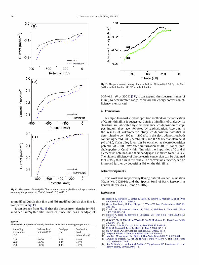
Fig. 12. The current of CuInS2 thin films as a function of applied bias voltage at variousannealing temperature. (a) 350 �C, (b) 400 �C, (c) 450 �C.
Fig. 13. The photocurrent density of unmodified and PbS modified CuInS2 thin films.(a) Unmodified thin film, (b) PbS modified thin film.
J. Yuan et al. / Vacuum 99 (2014) 196e203202
unmodified CuInS2 thin film and PbS modified CuInS2 thin film iscompared in Fig. 13.
It can be seen from Fig. 13 that the photocurrent density for PbSmodified CuInS2 thin film increases. Since PbS has a bandgap of
Table 6The electric properties of CuInS2 thin films at various annealing temperature.
Annealingtemperature(�C)
Valence bandpotential (eV)
Bandgap(eV)
Conductionbandpotential (eV)
350 �0.30 1.59 �1.89400 �0.30 1.49 �1.79450 �0.30 1.48 �1.78
0.37e0.41 eV at 300 K [37], it can expand the spectrum range ofCuInS2 to near infrared range, therefore the energy conversion ef-ficiency is enhanced.
4. Conclusion
A simple, low-cost, electrodeposition method for the fabricationof CuInS2 thin films is suggested. CuInS1.5 thin films of chalcopyritestructure are fabricated by electrochemical co-deposition of cop-pereindium alloy layer, followed by sulphurization. According tothe results of voltammetric study, co-deposition potential isdetermined to be �800 to �1100 mV. In the electrodeposition bathcontaining 5 mM CuCl2, 5 mM InCl3 and 0.2 M triethanolamine atpH of 4.0, Cu2In alloy layer can be obtained at electrodepositionpotential of �1000 mV; after sulfurization at 400 �C for 90 min,chalcopyrite p- CuInS1.5 thin film with the impurities of C and Oelements is obtained, and their bandgap is estimated to be 1.49 eV.The highest efficiency of photoelectric conversion can be obtainedfor CuInS1.5 thin film in this study. The conversion efficiency can beimproved further by depositing PbS on the thin films.
Acknowledgments
This work was supported by Beijing Natural Science Foundation(Grant No. 2102034) and the Special Fund of Basic Research inCentral Universities (Grant No. 1107).
References
[1] Jackson P, Hariskos D, Lotter E, Paetel S, Wuerz R, Menner R, et al. ProgPhotovoltaics 2011;19:894e7.
[2] Green MA, Emery K, King DL, Igari S, Warta W. Prog Photovoltaics 2002;10:235e41.
[3] Krunks M, Bijakina O, Varema T, Mikli V, Mellikov E. Thin Solid Films1999;338:125e30.
[4] Bollero A, Trigo JF, Herrero J, Gutiérrez MT. Thin Solid Films 2009;517:2167e70.
[5] Onishi T, Abe K, Miyoshi Y, Wakita K, Sao N, Mochizuki K. J Phys Chem Solids2005;66:1947e9.
[6] Rabeh M, Zribi M, Kanzari B. Mater Lett 2005;59:3164e8.[7] Zribi M, Kanzari B, Rezig B. Mater Sci Eng B 2008;149:1e6.[8] Liu XP, Shao LX. Surf Coatings Technol 2007;201:5340e3.[9] Seeger S, Ellmer K. Thin Solid Films 2009;517:3143e7.
[10] Nikolaus M, Alexander M, Dieter S. Thin Solid Films 2007;515:5979e84.[11] Krunks M, Bijakina O, Rebane H, Oja I, Mikli V, Mere A. Thin Solid Films
2002;403e404:71e5.[12] Bini S, Bindu K, Lakshimi M, Sudha C, Vijayakumar KP, Kashiwaba Y, et al.
Renew Energy 2000;20:405e13.

J. Yuan et al. / Vacuum 99 (2014) 196e203 203
[13] Martinez AM, Arriaga LG, Fernández AM, Cano U. Mater Chem Phys 2004;88:417e20.
[14] Xu XH, Wang F, Liu JJ, Park KC, Fujishige M. Sol Energy Mater Sol Cells2011;95:791e6.
[15] Martinez AM, Fernández AM, Arriaga LG, Cano U. Mater Chem Phys 2006;95:270e4.
[16] Wijesundera RP, Siripala W. Sol Energy Mater Sol Cells 2004;81:147e54.[17] Nakamura S, Yamamoto A. Sol Energy Mater Sol Cells 2003;75:81e6.[18] Lee SM, Ikeda S, Yagi T, Harada T, Ennaoui A, Matsumura M. Phys Chem Chem
Phys 2011;13:6662e9.[19] Herrero J, Ortega J. Sol Energy Mater 1990;20:53e65.[20] Antony A, Asha AS, Yoosuf R, Manoj R, Jayaraj MK. Sol Energy Mater Sol Cells
2004;81:407e17.[21] Lincot D, Guillemoles JF, Taunier S, Guimard D, Sicx-Kurdi J, Chaumont A, et al.
Sol Energy 2004;77:725e37.[22] Huang Q, Reuter K, Amhed S, Deligianni L, Romankiw LT, Jaime S, et al.
J Electrochem Soc 2011;158(2):D57e61.[23] Chen G, Wang L, Sheng X, Chang L, Luo Y, Yang D. Phys Status Solidi A
2011;208:2399e405.
[24] Chen G,Wang L, Sheng X, Liu H, Pi X, Yang D. J Alloy Compd 2010;507:317e21.[25] Wang W, Xiong J, Zhu C, Jiang G. Chin J Chem Phys 2010;23:465e8.[26] Yuan J, Hao C. Sol Energy Mater Sol Cells 2013;108:170e4.[27] Barton EE, Rampulla DM, Bocarsly AB. J Am Chem Soc 2008;130:6342e4.[28] Zhang Z, Wang P. J Mater Chem 2012;22:2456e64.[29] Cayzac R, Boulc’h F, Bendahan M, Pasquinelli M, Knauth P. C R Chime 2008;11:
1016e22.[30] Joswig A, Gossla M, Metzner H, Reislohner U, Hahn T, Witthuhn W. Thin Solid
Films 2007;515:5921e4.[31] Gossla M, Mahnke HE, Metzner H. Thin Solid Films 2000;361e362:56e60.[32] Hertz J, Aissaoui KE, Bouirden L. J Phase Equilibria 2002;23:473e9.[33] Zouaghi MC, Ben Nasrallah T, Marsillac S, Bernè de JC, Belgacem S. Thin Solid
Films 2001;382:39e46.[34] Pankove JI. Optical processes in semiconductors. 1st ed. New Jersey: Prentice-
Hall Englewood Cliffs; 1971.[35] Tauc J, Menth A. J Non-Cryst Solids 1972;8:569e85.[36] Morrison SR. Electrochemistry at semiconductor and oxide metal electrodes.
1st ed. New York: Plenum Press; 1980.[37] Sambur JB, Novet T, Parkinson BA. Science 2010;330:63e6.