fabrication of high refractive index, periodic, …
TRANSCRIPT

University of Massachusetts Amherst University of Massachusetts Amherst
ScholarWorks@UMass Amherst ScholarWorks@UMass Amherst
Doctoral Dissertations Dissertations and Theses
November 2018
FABRICATION OF HIGH REFRACTIVE INDEX, PERIODIC, FABRICATION OF HIGH REFRACTIVE INDEX, PERIODIC,
COMPOSITE NANOSTRUCTURES FOR PHOTONIC AND SENSING COMPOSITE NANOSTRUCTURES FOR PHOTONIC AND SENSING
APPLICATIONS APPLICATIONS
Irene Howell University of Massachusetts Amherst
Follow this and additional works at: https://scholarworks.umass.edu/dissertations_2
Part of the Ceramic Materials Commons, Polymer and Organic Materials Commons, and the
Semiconductor and Optical Materials Commons
Recommended Citation Recommended Citation Howell, Irene, "FABRICATION OF HIGH REFRACTIVE INDEX, PERIODIC, COMPOSITE NANOSTRUCTURES FOR PHOTONIC AND SENSING APPLICATIONS" (2018). Doctoral Dissertations. 1441. https://doi.org/10.7275/12639590 https://scholarworks.umass.edu/dissertations_2/1441
This Open Access Dissertation is brought to you for free and open access by the Dissertations and Theses at ScholarWorks@UMass Amherst. It has been accepted for inclusion in Doctoral Dissertations by an authorized administrator of ScholarWorks@UMass Amherst. For more information, please contact [email protected].

FABRICATION OF HIGH REFRACTIVE INDEX, PERIODIC, COMPOSITE
NANOSTRUCTURES FOR PHOTONIC AND SENSING APPLICATIONS
A Dissertation Presented
by
IRENE R. HOWELL
Submitted to the Graduate School of the
University of Massachusetts Amherst in partial fulfillment
of the requirements for the degree of
DOCTOR OF PHILOSOPHY
September 2018
Polymer Science & Engineering

© Copyright by Irene R. Howell 2018
All Rights Reserved

FABRICATION OF HIGH REFRACTIVE INDEX, PERIODIC, COMPOSITE
NANOSTRUCTURES FOR PHOTONIC AND SENSING APPLICATIONS
A Dissertation Presented
by
IRENE R. HOWELL
Approved as to style and content by:
____________________________________
James Watkins, Chair
____________________________________
Kenneth Carter, Member
____________________________________
Jae-Hwang Lee, Member
________________________________________
E. Bryan Coughlin, Department Head
Polymer Science & Engineering

DEDICATION
To my family.
v
ACKNOWLEDGMENTS
I would like to thank my thesis advisor, Professor James Watkins, who has given
me the opportunity to work in his research group. I have really appreciated all of the
opportunities to work on interesting projects, attend conferences and workshops, and to
travel to many new places that have helped me grow. I would also like to thank my
committee members, Professor Kenneth Carter and Professor Jae-Hwang Lee for their
contributions to my development as a scientist, as well as their flexibility in scheduling!
I would also like to acknowledge and thank my collaborators for their good ideas
and contributions to the projects we worked on. I would like to thank Andreas Schedl
from the University of Bayreuth for his initiation and work on the polymeric gradient
materials, Dr. Dieter Nees for his contributions to the patterning of high refractive index
composite materials, Dr. Marc Verschuuren from Philips Research for the opportunity to
learn about SCIL technology, and Dr. Baptiste Giroire from the University of Bordeaux
for his help on the nitridation of TiO2 work.
I would also like to thank members of the Watkins group for their contributions
to my research: Rohit Kothari for his initial work on the direct patterning of TiO2
nanoparticle-based inks and fabrication of 3D photonic crystals, Shengkai Li for his help
with the XPS measurements of nitrided TiO2 films, and Feyza Dundar for her helpful
ideas and experiments that resulted in some of the successful high aspect ratio imprinting
techniques. And of course, I would like to acknowledge and thank all other members of
the Watkins group for their day-to-day discussions, tips, suggestions, and general
friendliness, making working alongside them very pleasant.

vi
The PSE department faculty and staff also deserve much appreciation for their
contributions making my dissertation research possible. Without staff, including Jo-Ann
Bourguignon, MaryAnn Mish, and Lisa Groth, it would have been much more difficult
to have navigate all logistical aspects of graduate school. I would specifically like to thank
Professor Alex Ribbe and Louis Raboin for their diligent care of the electron microscope
and John Nicholson for his help with the cleanroom equipment, on which I have depended
for much of my research.
I would also like to thank my undergraduate research advisor, Dr. Eugene Joseph,
who was extremely supportive, provided great projects for me to work on, and overall
provided a wonderful opportunity for me during my time at Virginia Tech. Without his
suggestion and encouragement, I would not have applied to the UMass PSE PhD
program.
Of course, without the encouragement, prayers, and support of my friends and
family, I would not have been able to accomplish anything.
“My grace is sufficient for you, for my power is made perfect in weakness.” Therefore, I will
boast all the more gladly about my weaknesses, so that Christ’s power may rest on me.
2 Cor. 12:9
vii
ABSTRACT
FABRICATION OF HIGH REFRACTIVE INDEX, PERIODIC, COMPOSITE
NANOSTRUCTURES FOR PHOTONIC AND SENSING APPLICATIONS
SEPTEMBER 1, 2018
IRENE R. HOWELL, B.S., VIRGINIA TECH
M.A., UNIVERSITY OF MASSACHUSETTS AMHERST
Ph.D., UNIVERSITY OF MASSACHUSETTS AMHERST
Directed by: Professor James J. Watkins
This dissertation examines methods of fabricating high refractive index, periodic
structures and their applications. Structures with a refractive index periodicity in one-
dimensionally are fabricated by stacking layers of (high-refractive index) nanoparticle-
filled and unfilled layers. More complex two- and three-dimensional structures are
fabricated by direct printing of nanoparticles via solvent-assisted soft nanoimprint
lithography.
Polymer-nanoparticle composites are an active area of research and development
especially for photonic applications. We show use of two composite formulations, first
for fabrication of one-dimensional photonic crystals, and second for scalable UV-
nanoimprinting. One dimensional photonic crystals, which possess a periodicity in
refractive index, result in a constructive interference-based reflectance peak, whose
location, intensity, and bandwidth can be tuned by controlling the contrast in refractive
index and the number of periods. Appropriate materials were selected to create a strain-
tunable, one-dimensional photonic crystal-based mechanochromic sensor. The same
material system and one-dimensional photonic crystal were used in conjunction with
viii
novel modulus-gradient elastomer substrates. When subjected to strain, the modulus
gradient resulted in unique, bio-inspired photonic gradient effects. UV-nanoimprinting
provides a convenient method for creating patterned surfaces. By incorporating high
refractive index additives, ZrO2 and N-vinyl carbazole, we achieve an imprint-able,
solvent-free, high refractive index UV-resin.
For applications requiring even higher refractive indices and more harsh
environments, polymer nanocomposites are not suitable. Direct patterning of
nanoparticles via solvent-assisted soft nanoimprint lithography is used to fabricate
periodic structures over large areas. Complex, three-dimensional woodpile structures
were successfully fabricated through layer-by-layer imprinting of TiO2 nanoparticle-
based dispersions. Similarly, imprinted TiO2 multidimensional nanostructures were
nitrided with high-temperature ammonia, resulting in multi-dimensional, nanostructured
plasmonic materials. We examine the crystal structure, atomic concentration, optical
properties as well as the resulting patterned structure after the nitridation process. Finally,
a post-imprinting densification method is demonstrated, in which the refractive index
TiO2 nanoparticle-based nanostructures can be tuned and dramatically increased. This
fast, inexpensive, and scalable method could be attractive for production of dielectric
metamaterials.

ix
TABLE OF CONTENTS
Page
ACKNOWLEDGMENTS ................................................................................................ v
ABSTRACT .................................................................................................................... vii
LIST OF TABLES .......................................................................................................... xii
LIST OF FIGURES ....................................................................................................... xiii
CHAPTER
1. INTRODUCTION ........................................................................................................ 1
1.1 Overview ......................................................................................................... 1 1.2 Refractive Index .............................................................................................. 3 1.3 Nanocomposites .............................................................................................. 7
1.4 Patterned and Periodic Nanostructures ......................................................... 10 1.5 Nanoimprint Lithography ............................................................................. 13 1.6 References ..................................................................................................... 16
2. HIGH REFRACTIVE INDEX POLYMER-NANOPARTICLE COMPOSITES ..... 21
2.1 Introduction ................................................................................................... 21 2.2 Strain-Tunable One-Dimensional Photonic Crystals Based on Zirconium
Dioxide/Slide-Ring Elastomer Nanocomposites for Mechanochromic
Sensing .......................................................................................................... 23
2.2.1 Background .................................................................................... 23 2.2.2 Experimental .................................................................................. 27
2.2.2.1 Materials ......................................................................... 27 2.2.2.2 Preparation of 1DPCs ..................................................... 28
2.2.2.3 Characterization .............................................................. 29
2.2.3 Results and Discussion .................................................................. 30
2.2.3.1 ZrO2-Slide Ring Composite Film Properties .................. 30 2.2.3.2 1DPC Fabrication and Charcterization ........................... 32 2.2.3.3 Sensor Behavior .............................................................. 35
2.2.4 Conclusions .................................................................................... 38
2.3 Gradient Photonic Materials ......................................................................... 38
2.3.1 Background .................................................................................... 38

x
2.3.2 Experimental .................................................................................. 40
2.3.2.1 Materials ......................................................................... 40
2.3.2.2 Preparation of Gradient Photonic Material ..................... 41 2.3.2.3 Characterization .............................................................. 42
2.3.3 Results and Discussion .................................................................. 43
2.3.3.1 Gradient PDMS ............................................................... 43 2.3.3.2 Optical Response: Linear Modulus Gradient .................. 44
2.3.3.3 Optical Response: Oscillating Modulus Gradient........... 46
2.3.4 Conclusions .................................................................................... 48
2.4 Scalable, UV-curable, Transparent, High-Refractive Index ZrO2
Nanoparticle Composite Resins for UV-Nanoimprint Lithography ............. 48
2.4.1 Background .................................................................................... 48 2.4.2 Experimental .................................................................................. 50
2.4.2.1 Materials ......................................................................... 50
2.3.2.2 Preparation of Composites .............................................. 50 2.4.2.3 Preparation of Nanopatterned and Smooth Films ........... 51
2.4.2.4 Preparation of Roll to Roll Stamps ................................. 51 2.4.2.5 Characterization .............................................................. 52
2.4.3 Results and Discussion .................................................................. 53
2.4.3.1 High Index Composite Components and
Refractive Index .............................................................. 53 2.4.3.2 Batch Imprinting of Resins ............................................. 57 2.4.3.3 Roll to Roll Demonstrations ........................................... 59
2.3.4 Conclusions .................................................................................... 59
2.5 Conclusions ................................................................................................... 60 2.6 References ..................................................................................................... 61
3. FABRICATION OF PLASMONIC TIN NANOSTRUCTURES BY NITRIDATION
OF NANOIMPRINTED TIO2 NANOPARTICLES .................................... 67
3.1 Introduction ................................................................................................... 67 3.2 Experimental ................................................................................................. 69
3.2.1 Materials ........................................................................................ 69 3.2.2 Preparation of PDMS Stamps ........................................................ 70 3.2.3 Preparation of Nanoparticle-based Solutions................................. 71

xi
3.2.4 Preparation of Planar and Patterned TiO2
Nanoparticle-based Films ................................................................. 71
3.2.5 Preparation of Perpendicular, Intersecting,
TiO2 Bilayer Gratings ....................................................................... 72 3.2.6 Nitridation Process ......................................................................... 75 3.2.7 Characterization ............................................................................. 75
3.3 Results and Discussion ................................................................................. 76
3.3.1 Planar Film Crystallinity and Composition ................................... 76 3.3.2 Patterned Sample Analysis ............................................................ 84 3.3.3 Optical and Plasmonic Response ................................................... 89
3.4 Conclusions ................................................................................................... 92 3.5 References ..................................................................................................... 93
4. DENSIFICATION AND TUNABILITY OF ALL-INORGANIC, HIGH-
REFRACTIVE INDEX TIO2 NANOPARTICLE-BASED FILMS AND
HIGH ASPECT RATIO NANOSTRUCTURES BY ALD ......................... 97
4.1 Introduction ................................................................................................... 97
4.2 Experimental ................................................................................................. 99
4.2.1 Materials ........................................................................................ 99 4.2.2 Preparation of Inverse Master and HPDMS/PDMS Stamps........ 100
4.2.3 Preparation of Densified Films .................................................... 102
4.2.4 Characterization ........................................................................... 103
4.3 Results and Discussion ............................................................................... 104
4.3.1 Temperature-based Densification ................................................ 104
4.3.2 ALD onto Planar Films ................................................................ 106 4.3.3 ALD onto Patterned Surfaces ...................................................... 111 4.3.4 ALD for Enhanced Photonic Structures ...................................... 115
4.3.5 Tunability of All-Inorganic TiO2 Films ....................................... 116
4.4 Conclusions ................................................................................................. 118 4.5 References ................................................................................................... 119
5. FINAL COMMENTS AND OUTLOOK ................................................................. 123
BIBLIOGRAPHY ......................................................................................................... 124

xii
LIST OF TABLES
Table Page
2-1. 1DPC Mechanochromic Sensitivity ........................................................................ 38
3-1. Heat treatments and calculated porosity of TiO2 films ............................................ 80
3-2. Atomic Concentrations (%) at 5 min sputter time ................................................... 81
4-1. TiO2 Deposition onto Bare Si ................................................................................ 107
4-2. Porosity Calculated from Lorentz-Lorenz Equation ............................................. 109
4-3. Changes in Feature Dimension Before and After ALD ........................................ 114

xiii
LIST OF FIGURES
Figure Page
1-1. a) Light refracting at the interface between two mediums and b) refractive
indices with observable dispersion. ...................................................................... 3
1-2. a) Ellipsometer measurement setup and b) flow chart for ellipsometry data
extraction............................................................................................................... 5
1-3. Reproduced from Reference 4. Schematic demonstrating preparation of
nanocomposites by a) in situ nanoparticle synthesis and b) blending of
pre-synthesized nanoparticles. .............................................................................. 8
1-4. Reproduced from Reference 16. Demonstration of the effect of particle size
and particle refractive index on transmission of composite for a 3 mm,
20% nanoparticle (by volume) composite where the matrix index is 1.5
and particle index is a) 4, b) 3, c) 2.5, d) 2, and e) 1.75. .................................... 10
1-5. One, two, and 3-dimensionally periodic structures. Reproduced from
reference 19. ........................................................................................................ 11
1-6. Reproduced from Reference 28. Photonic stopband reflection intensity from
Bragg reflectors. Intensity of reflection depends on refractive index
contrast and number of periods, N. Solid line, N = 3, dashed line, N = 10. ....... 12
1-7. Reproduced from Reference 44. Process outline for patterning via electron
beam lithography. ............................................................................................... 14
2-1. Alternating high refractive index (n1) and low refractive index (n2) layers
with constructive interference. The optical thickness (n*d) of each layer
is one-fourth of the center wavelength to be reflected. ....................................... 24
2-2. Visualization of Equation 3 assuming layer n2 = 1.5. ............................................. 25
2-3. a) Schematic structure of slide ring elastomers. Reprinted (adapted) with
permission from Reference 20. Copyright (2011) American Chemical
Society. b) The chemical structure of SeRM Super Polymer AU1000 is
shown. Once interlocked with other chains, these form the slide ring
network. .............................................................................................................. 27
2-4. Schematic demonstrating fabrication of high-low index bilayers. .......................... 29
2-5. a) Photograph of straining plate under Filmetrics F40, b) photograph of
straining plate, and c) illustration of film before and after strain is
applied. ................................................................................................................ 30

xiv
2-6. a) Transmission spectra of 5 layers of 70 wt% ZrO2 in UV-cured slide ring
elastomer and b) TEM image of ZrO2 nanoparticles dispersed within a
slide ring elastomer matrix at 70 wt% nanoparticles. Scale bar is 80 nm. ......... 31
2-7. a) Refractive index of various nanocomposite compositions and b) SEM
image of a 5 bilayer 1DPC consisting of alternating filled (70 wt% ZrO2)
and unfilled Slide-Ring elastomers. The bottom-most layer is a water-
soluble sacrificial layer of polyvinyl alcohol on silicon. .................................... 33
2-8. Film thicknesses from spin coated films. The error between sample
thicknesses are 4.02, 4.1, and 4.4 nm, respectively. The overall standard
deviation of the film thicknesses is 1.6 nm. ........................................................ 34
2-9. Simulated and experimental reflectance spectrum for 70 wt% ZrO2
composite 1DPCs containing 6 periods. ............................................................. 35
2-10. a) Reflectance spectra of a 6 period 1DPC under increasing strain (0 to
42%), b) peak reflected wavelength as a function of strain, and c) digital
photographs of 6-layer 1DPC under increasing strain from 0% (red) to
approximately 40% (blue). .................................................................................. 36
2-11. Mechanochromic sensitivity of 6 period 1DPC over 100 runs after 4
months at a set strain of less than 10%. .............................................................. 37
2-12. Schematic (a) and photograph (b) of unstrained 1DPC on linear gradient
PDMS strip and c) normalized reflectance of unstrained linear gradient
1DPC. .................................................................................................................. 45
2-13. Schematic (a) and photograph (b) of strained (25%) 1DPC on linear
gradient PDMS strip and c) normalized reflectance of strained linear
gradient 1DPC (25%). ......................................................................................... 46
2-14. Schematic (a) and photograph (b) of strained (25%) 1DPC on oscillating
gradient PDMS strip and c) normalized reflectance of strained oscillating
gradient 1DPC (25%). ......................................................................................... 47
2-15. Schematic of aluminum mastering plate with 1in2 slots for masters(a),
mastering plate fitted with diverse test patterns on 1 in2 substrates for
stamp preparation (b), test pattern stamp wrapped around drum (c),
photograph of mastering plate with vacuum connections (d), and
photograph of R2R UV-NIL with PET web (1), plasma treatment (2),
gravure coater (3), and UV-NIL stage (4). ......................................................... 52
2-16. Chemical structure of a) M1142 (o-phenylphenol ethyl acrylate) and b) N-
vinylcarbazole. .................................................................................................... 53

xv
2-17. Refractive index of M1142 with increasing ZrO2 loading (a), and
refractive index of M1142/NVC composites. Both measured before
curing with 3% photoinitiator added................................................................... 54
2-18. NVC on glass. Scale bar is 20 µm. ........................................................................ 55
2-19. Refractive index (λ = 589 nm) of M1142/NVC compositions with
increasing ZrO2 loading (a), refractive index versus wavelength of cured
films of various compositions (b), and UV-Vis spectra of various cured
150 µm films (c). ................................................................................................ 57
2-20. Imprints of M1142 with a) 0 vol% ZrO2 and b) 30 vol% ZrO2 and Imprints
of M1142/NVC 8/3.25 with c) 0% ZrO2 and d) 30 vol% ZrO2 Scale bars
are 20 µm. ........................................................................................................... 58
2-21. Height profiles of imprinted M1142 (a, b) and height profiles of imprinted
M1142/30 vol% ZrO2 (c, d). ............................................................................... 59
3-1. a) Fabrication method for patterned TiO2 and TiN films, b) cm-scale PDMS
stamps and imprinted gratings on silicon, and c) large-area SEM image
of uniform, defect-free, imprinted gratings. ........................................................ 72
3-2. Schematic illustrating the process used to create intersecting, residual-layer-
free bilayer gratings by a) coating with PMMA, b) imprinting and
PMMA lift-off, c) planarizing, d) coating with PMMA, e) imprinting, f)
PMMA lift off and calcination, g) nitridation and electrode deposition............. 73
3-3. TiO2 intersecting residual-layer-free bilayer imprints at different
magnifications (a-c). ........................................................................................... 74
3-4. Standard XRD of a) TiO2 films before and after 2, 4, and 6-hour treatments,
and b) low incidence XRD of treated film from 0.1 to 3o................................... 77
3-5. XPS data showing atomic concentration (AC) vs sputter time of different
elements for a) untreated TiO2, b) 2-hour ammonia treatment, c) 4-hour
ammonia treatment, and d) 6-hour ammonia treatment. ..................................... 78
3-6. Ellipsometric data of annealed TiO2 films fit using the Cauchy model. ................. 80
3-7. a) TiO2 NP film heated at 475oC for 4 hours and b) after 6-hour nitridation
treatment (NH3, 1000oC). Scale bars are 1 µm. .................................................. 81
3-8. XPS binding energies for a) Ti2p, b) N1s, and O1s orbitals of: TiO2
nanoparticle films (untreated), treated films (for 2, 4, and 6 hours), and a
reference TiN film............................................................................................... 84
3-9. SEM images of a) single layer lines and b) double layer lines of TiO2.
Samples heated for 6 hours at 1000oC. Scale bars 3 µm. ................................... 85

xvi
3-10. a) TiO2 NP-only bilayer woodpiles before (a) and after (c) nitridation and
TiO2 NP with sol-gel precursor before (b) and after (d) nitridation. Scale
bar is 2 µm. ......................................................................................................... 86
3-11. SEM images before (a-c) and after (d-e) 6-hour nitridation treatment. Top
views of single layer (a, d) and bilayer (b, e), and tilted (8o) and rotated
(45o) cross-sectional views (c, f) of bilayer samples shown. All scale bars
are 3 µm. ............................................................................................................. 87
3-12. Mapping of Si on untreated TiO2 patterned lines. Scale bar is 3 µm. ................... 88
3-13. Elemental mapping of patterned samples before (a-d) and after (e-l) 6-hour
nitridation treatment for titanium (b, f, j), oxygen (c, g, k), nitrogen (d, h,
l). Scale bars are 3 µm. Colors are false, and contrast/brightness has been
adjusted for visibility. ......................................................................................... 88
3-14. Real (Ɛ’) and imaginary (Ɛ”) dielectric constants of planar films a) of TiO2
before nitridation and b) of 2, 4, and 6 hr nitridated ftn90 samples. .................. 90
3-15. Measurement of SPP on nitrided TiO2 nanostructures (a), 2 hour (b) and 6
hour (c) treated samples. ..................................................................................... 91
4-1. a) Steps to fabricate an inverse-tone master in order to obtain imprinted
TiO2 pillars and b) photograph of a replica master. .......................................... 101
4-2. Measured refractive index of planar TiO2 NP films after different 4-hour
heat treatments (a), and corresponding XRD patterns of the same films
(b). ..................................................................................................................... 105
4-3. Top-view SEM images of TiO2 films treated at a) 50, b) 475, c) 600, and d)
750oC for 4 hours. Scale bars are 1 µm. ........................................................... 106
4-4. Process overview showing solvent-assisted NIL technique, followed by
ALD densification. ............................................................................................ 107
4-5. a) Refractive indices (nD) and thicknesses of TiO2 NP films after 25, 50,
150, and 380 ALD cycles, b) refractive indices vs wavelength of TiO2
NP films before ALD (green), after ALD (blue) of TiO2 ALD onto bare
silicon, and SEM images of c) NP film with no ALD, d) 50 cycles of
ALD, and e) 150 cycles of ALD. ...................................................................... 108
4-6. a) film refractive index before (black) and after (red) ALD treatment for
various numbers of cycles, and b) calculated shrinkage of films after
heating at 475oC for 4 hrs. ................................................................................ 110
4-7. AFM images of TiO2 nanoparticle films before and after ALD. ........................... 111

xvii
4-8. Tilted cross section and closeup (inset) of imprinted TiO2 NP-based
gratings before (a) and after (b) 100 cycles of Al2O3 deposition, and EDS
images of a grating cross section (c) showing aluminum (d), oxygen (e),
and titanium (f). ................................................................................................ 111
4-9. Large area top (a) and tilted cross-sectional view (b) of imprinted TiO2 NP
pillars. Top and cross-sectional views of polymer imprint (c, e) and, top
and cross-sectional view of TiO2 NP imprint (d, f). ......................................... 113
4-10. Cross section and tilted view of TiO2 imprinted pillars before ALD (a, c)
and cross section and tilted view of TiO2 imprinted pillars after ALD. ........... 115
4-11. Experimental transmission and reflection intensity of 4-layer woodpile
structures before and after ALD. ...................................................................... 116
4-12. a) Refractive index and calculated porosity of TiO2 NP films subjected to
2, 5, 10, and 15 cycles of ALD, b) spin coated TiO2 film subjected to
consecutive rounds of 2 ALD cycles, c) refractive index and d) thickness
map of gradient sample, and e) refractive index dispersion along x = 0 of
gradient sample. ................................................................................................ 118

1
CHAPTER 1
INTRODUCTION
1.1 Overview
Within this dissertation we discuss the fabrication and characterization of various
periodic nanostructured materials with a focus on high refractive index materials and their
applications. Specific focus is given to nanoparticle-based structures in which
nanoparticles are either incorporated into a polymeric matrix to generate high refractive
index composite materials or are used directly in patterning without a polymeric matrix.
In this chapter, several concepts are introduced, and a brief background is given noting
their significance in the chapters following. Refractive index, nanocomposites, patterned
and periodic structures, and nanoimprint lithography are discussed and help provide
context to the rest of the dissertation.
Chapter 2 describes the formulation of two similar high refractive index
ZrO2/polymer composites for three different applications. The first composite consists of
high refractive index ZrO2 nanoparticles dispersed within an elastomeric matrix and is
solution processed via spin coating to create thin films. We characterize the composite
transmission and refractive index, and then demonstrate the fabrication of a strain-tunable
one-dimensional photonic crystal, or Bragg mirror, based on alternating nanoparticle
filled and unfilled elastomer layers. Due to the film’s elasticity, when strained the layer
thicknesses decrease, resulting in a shift in the Bragg reflectance peak. We discuss its use
as a mechanochromic sensor including sensitivity and durability. We then shift and
examine the effect of a gradient modulus elastic substrate on the reflectance behavior of
the photonic crystal film. We discuss the inspiration from nature of both gradient

2
materials and photonic crystals and demonstrate the clear effects of a simple linear
modulus gradient and of a more complex, chameleon-inspired, oscillating modulus
gradient on the colorful reflectance from our film. Finally, in the last section of Chapter
2, we modify our high refractive index composite formulation to be suitable for large
scale UV-nanoimprinting. As volatile solvents are often undesirable for large scale
processing, we formulated a UV-curable, high refractive index composite using ZrO2
nanoparticles, UV resin Miramer 1142, and small molecule NVC. Components were
selected for their relatively high refractive indices. In the final formulation, we
demonstrate UV-nanoimprinting of composites with refractive indices above 1.7.
In Chapter 3, we discuss the fabrication of a patterned, multi-dimensional
nanostructures using solvent assisted nanoimprint lithography. Solvent assisted
nanoimprint lithography allows for the direct patterning and focuses on using the method
as a controllable, versatile method of fabricating plasmonic nanostructures. TiO2 line
gratings and bilayer woodpiles are patterned and then nitridated under hot ammonia gas,
resulting in the conversion from anatase TiO2 to TiN. This chapter focuses on the
fabrication methods and the characterization of the resulting nitrided TiO2. The crystal
structure, elemental composition, and optical properties are analyzed and discussed.
Overall the method offers a convenient method for fabricating patterned, multi-
dimensional plasmonic materials.
Chapter 4 presents an alternative, scalable, fast, and relatively inexpensive method
for fabricating high aspect ratio, high refractive index, patterned surfaces which can be
used in producing dielectric metamaterials. The process consists of two main steps: the
direct patterning of high aspect ratio TiO2 nanoparticle-based nanopillars, and the post-

3
patterning densification by atomic layer deposition. We discuss the inherent porosity of
nanoparticle-based films and patterns and the resulting decrease in refractive index,
relative to the bulk, and improvement through heat and using ALD to conformally fill the
pores with TiO2. The resulting TiO2 nanoparticle-based pillars have aspect ratios up to
6.3 and is the first demonstration of its kind. Such techniques could be attractive for
scalable production of metamaterials like metalenses.
1.2 Refractive Index
Refraction can be observed in daily life, such as the altered appearance of a straw
in a glass of water and is a result of the bending of light as it encounters the boundary
between two materials with different properties, as shown in Figure 1-1a.
Figure 1-1. a) Light refracting at the interface between two mediums and b) refractive
indices with observable dispersion.
A material’s refractive index is a fundamental material property which depends on the
molecular makeup, and describes how light will pass through a material according to the
definition:
𝑛 = 𝑣
𝑐,
a. b.

4
where n is the refractive index, v is the velocity of light in the material, and c is the speed
of light in a vacuum (the refractive index of air (vacuum) being 1). When light reaches a
material interface, the degree of bending, θ, will depend on the refractive indices, n, of
the mediums, and will follow Snell’s law:
𝑛1𝑠𝑖𝑛𝜃1 = 𝑛2𝑠𝑖𝑛𝜃2.
A material’s refractive index depends on its molecular makeup, specifically its
electric susceptibility which is related to the polarizability of a material in the presence
of an electric field. Light, or electromagnetic radiation, incident on an electrically
susceptible material will result in a change in the light’s velocity, giving rise to the
material’s refractive index. The complex refractive index,
𝑛 = 𝑛 + 𝑖𝑘
consists of the real refractive index, n, and also contains an imaginary component, known
as the extinction coefficient, k. The extinction coefficient describes the light that is
absorbed by the material. For most materials, the complex refractive index varies with
wavelength, which is referred to as dispersion (Figure 1-1b), and can be described with
the Abbe number:
𝑉 =𝑛𝑦𝑒𝑙𝑙𝑜𝑤−1
𝑛𝑏𝑙𝑢𝑒−𝑛𝑟𝑒𝑑,
Where nyellow, nblue, and nred refer to the refractive index values in these wavelength
regions. Additionally, other empirical models used to describe the refractive index
dispersion include the Cauchy and Sellmeier equations. The Cauchy model:
𝑛(𝜆) = 𝐴 +𝐵
𝜆2 +𝐶
𝜆4,

5
where A, B, and C are constants, can be used to describe the refractive index of a
transparent material (k = 0). Ellipsometry is a commonly used technique to obtain these
optical constants.
Ellipsometry measures the change polarization after reflecting from (or
transmitting through) a material, as shown in Figure 1-2a. The two measured
ellipsometric variables, Ψ and Δ, can be fit to various models, depending on the basic
characteristics of the material of interest. For variable angle, spectroscopic ellipsometry,
the optical constants and thickness can be extracted simultaneously, following the
procedure in Figure 1-2b.
Figure 1-2. a) Ellipsometer measurement setup and b) flow chart for ellipsometry data
extraction.
a.
b.

6
Ellipsometry provides a powerful tool for characterizing optical properties of films,
including more complex models such as oscillator models based on Lorentzian
oscillators, as well as the possibility to measure thicknesses and optical constants of
multiple distinct film layers. However, as the complexity of the model increases, the
uncertainty in the accuracy of the results may increase, requiring additional confirmatory
experiments.
Different types of materials predictably possess different ranges of refractive
indices. Most gases have refractive indices close to 1, while solids generally have values
above 1.3. For example, visibly transparent dielectric materials such as glass typically
have values between 1 and 2 (measured in the visible region), while some semiconductors
such as silicon or germanium have values up to 3 or 4 (measured in the infrared region).
Most organic materials, including polymers, have refractive indices close to 1.5, usually
ranging from 1.3 to 1.7, with some exceptions. Aerogels for example possess extremely
low refractive indices, as low as 1.0131,2, due to their unique structures and low density.
On the other hand, there continues to be great interest in high refractive index polymers
for optoelectronic applications, LED encapsulants, and lenses. Many polymers have been
designed to increase refractive index to target these applications, however, for most
applications it is also important to pay attention to the Abbe number, optical transparency,
and birefringence. Many high index polymers (n > 1.7) contain aromatic groups and
conjugated structures, and their usefulness is limited due to limited visible transparency,
high dispersion, and poor solubility, which limits processability3,4. Due to the continued
desire for high index polymers and the aforementioned limitations of synthesizing

7
suitable polymers, polymer nanocomposites have proven an effective alternative strategy,
and will be discussed further in the following section.
1.3 Nanocomposites
Nanotechnology, and specifically polymer nanocomposites have permeated many
fields of technology5,6 including electronics, mechanics, photonics, biomaterials, and
even cosmetics. As technology continues to move forward, the need for more advanced
materials and materials with improved properties continues to grow with polymer
nanocomposites presenting one route to these advanced materials. Some of the more well-
known nanocomposites are the clay-reinforced resin materials7 and the carbon black-
toughened car tires8. These nanocomposites afforded improved mechanical properties,
eventually contributing to the interest and research into many different aspects of
nanoparticle and polymer composites. Many of the advances in nanocomposites can be
attributed to improvements and advances in controlling nanoparticle synthesis and
surface modification, as well as the instrumentation to observe them.
In order to be effective and to possess improved properties, nanoparticles within
a polymeric host must be well dispersed and not aggregated, which has been the topic of
many research publications4,6,9. Nanoparticle-polymer interactions must be considered to
prevent nanoparticle aggregation and phase separation between the host and filler
material. Well-dispersed nanocomposite materials can be achieved by controlling the
interactions between the nanoparticle surface and the host material. Surface
modification/functionalization with small molecule or polymeric ligands provide a
convenient method of controlling these interactions and enabling high loadings of
nanoparticles with controlled distribution within specified phases of block copolymers10–
8
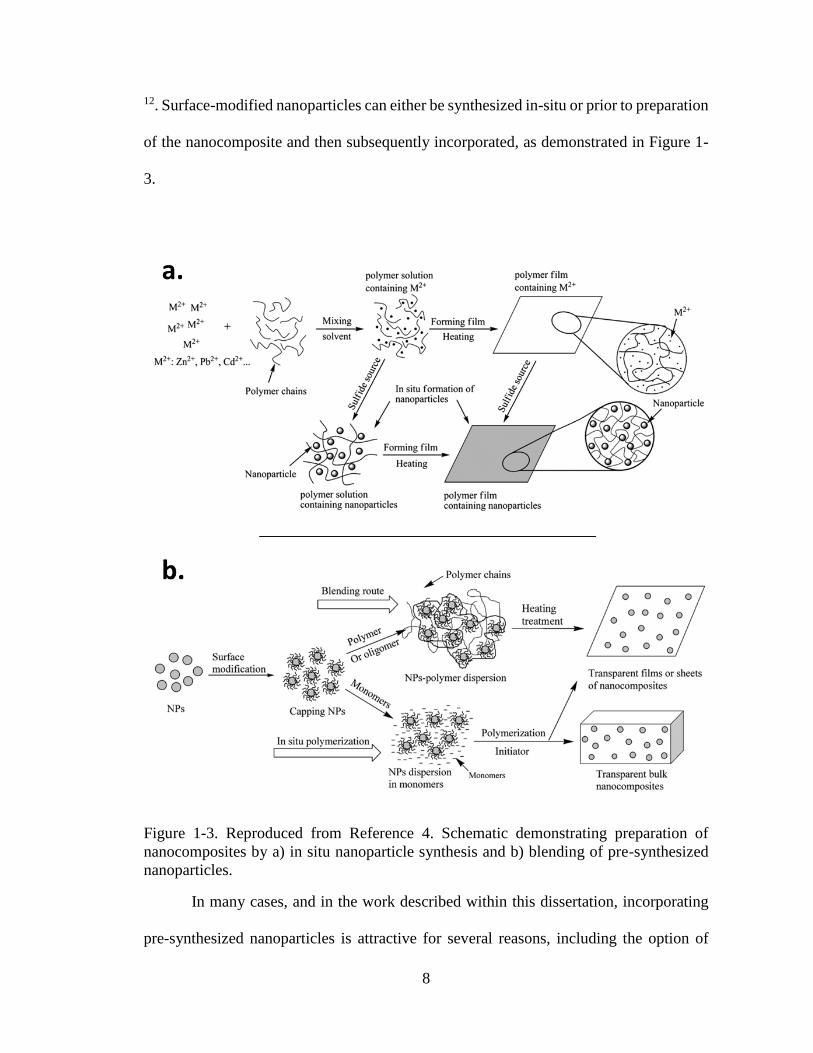
12. Surface-modified nanoparticles can either be synthesized in-situ or prior to preparation
of the nanocomposite and then subsequently incorporated, as demonstrated in Figure 1-
3.
Figure 1-3. Reproduced from Reference 4. Schematic demonstrating preparation of
nanocomposites by a) in situ nanoparticle synthesis and b) blending of pre-synthesized
nanoparticles.
In many cases, and in the work described within this dissertation, incorporating
pre-synthesized nanoparticles is attractive for several reasons, including the option of

9
using commercially available nanoparticles and the possibility of using inorganic
crystalline nanoparticles. Crystalline nanoparticles (nanocrystals), which require
synthetic temperatures not suitable for polymers, offer many attractive properties,
including high refractive indices, which is of central interest to this work.
For high refractive index polymer-nanoparticle composites for optical
applications specifically, optical transmission is must be considered. To achieve useful
composites that are transparent in the designed wavelength region, nanoparticle chemical
makeup, size, concentration, surface chemistry, as well as composite preparation and
thickness. Materials such as silicon, germanium, and lead sulfide are known for their high
refractive indices (n = 3-4), however, due to their absorption, their optical applications
are limited to those in the near infrared/infrared region. Particle size is also very important
in fabricating transparent composites; nanoparticles should be small enough to achieve
an effective medium in which nanoparticle inclusions within a matrix behave as a
homogenous medium13–15. In general, the size of the nanoparticle should be less than one
tenth of the wavelength of interest. Figure 1-4 shows the dependence of transmission on
particle size and refractive index. Here, transmission losses due to scattering arise from
large particles and large contrast in refractive indices of the filler and matrix. However,
even composites with large refractive index contrast can be achieved by using sufficiently
small nanoparticles.

10
Figure 1-4. Reproduced from Reference 16. Demonstration of the effect of particle size
and particle refractive index on transmission of composite for a 3 mm, 20% nanoparticle
(by volume) composite where the matrix index is 1.5 and particle index is a) 4, b) 3, c)
2.5, d) 2, and e) 1.75.
These high refractive index materials can be coated onto surfaces to provide UV
protection on transparent surfaces, reflective, anti-reflective or light-filtering coatings17,
as well as in improved LEDs encapsulants and high-performance displays18.
Additionally, the patterning of these high refractive index materials provides accessibility
of even more applications, as discussed in the next section.
1.4 Patterned and Periodic Nanostructures
Periodic nanostructures have found uses in many fields including optics,
photonics, electronics, as well as in biomedical applications. Though periodic
nanostructures have existed in nature for a very long time and are responsible for the
characteristic blue color of the Morpho butterfly wings for example, these small structures
remained unstudied and unable to be reproduced by researchers until advances in

11
microscopy and nanofabrication techniques were introduced. Since then, one major focus
of periodic nanostructures has been on molding the flow of light.
Figure 1-5. One, two, and 3-dimensionally periodic structures. Reproduced from
reference 19.
Some applications of periodic nanostructures in photonics have included
waveguides20, materials with photonic bandgaps21–24, flat lenses25, artificial magnetism,
and negative refractive indices26,27. Photonic bandgap materials, or photonic crystals,
consist of a refractive index periodicity in one, two, or three dimensions, as shown in
Figure 1-5. This specific design allows the formation of a photonic bandgap which,
analogous to semiconductors, excludes light of specific frequencies from propagating
within the medium. The excluded light is reflected based on Bragg’s law. Depending on
the degree of refractive index contrast, number of periods, and the geometry of the
periodic structure, the medium may exhibit a full photonic bandgap in which all light of
a specific frequency is reflect regardless of incident angle, or a stop band, in which not
all of the light of specific frequency is reflected28.

12
Figure 1-6. Reproduced from Reference 28. Photonic stopband reflection intensity from
Bragg reflectors. Intensity of reflection depends on refractive index contrast and number
of periods, N. Solid line, N = 3, dashed line, N = 10.
Periodic structures with a photonic stop band will exhibit reflection over a range of
wavelengths for which the structure can be specifically designed, like those demonstrated
in Figure 1-6. In the visible region of the electromagnetic spectrum this will result in
structural color and will be discussed further in Chapter 2.
Additionally, periodic structures fabricated from plasmonic materials have
applications in sensing29–31, structural color32, metamaterials33,34, optical absorbers35, and
photovoltaic devices36. Metamaterials need not be fabricated solely from plasmonic
materials, and benefit in certain ways from being all-dielectric, which is the discussed
further in Chapter 5. The field of plasmonics centers around the interactions of
electromagnetic radiation (light) with electrons at a dielectric/metallic interface, which
have two main manifestations: surface plasmon polaritons (SPPs) and localized surface
plasmon resonances (LSPRs). SPPs are electromagnetic excitations that occur at and

13
propagate along a dielectric/metal (conductor) interface as a result of coupling between
the electromagnetic field and the conductors’ electron oscillations. Due to momentum
mismatch, SPPs cannot be excited at a planar dielectric/metal interface. To excite them,
the prism coupling method or patterned surfaces can be utilized. LSPRs are non-
propagating excitations of electrons at the dielectric/metallic interface which can be
excited directly unlike SPPs. Periodic arrays of metallic nanoparticles can be used for
surface enhanced Raman spectroscopy (SERS)37. Another plasmonic applications
enabled by patterned surfaces is extraordinary optical transmission (EOT), in which light
transmission through sub-wavelength periodic apertures is enhanced by SPPs38. A large
range of structural colors based on plasmonic resonances have also been demonstrated by
fabricating nanodisk arrays with carefully controlled disk diameters and spacings
allowing for “color printing” without the need for pigments 32. The fabrication and use of
patterned plasmonic nanostructures will be discussed further in Chapter 4, while general
fabrication of nanostructures will be discussed in the next section.
1.5 Nanoimprint Lithography
Methods of fabricating patterned, and/or periodic nanostructures have developed
largely as a result of progress in the semiconductor industry, particularly due to the
continual miniaturization of integrated circuit components based on Moore’s Law.
Different forms of optical lithography have dominated patterning for the last fifty years
as device sizes and minimum patterned feature sizes have shrunk39, including projection
photolithography40, extreme UV (EUV), electron, and ion beam lithography41,42. While
these traditional lithography methods can lead to the fabrication of very uniform features
with resolution on the sub-10 nm level43, they are not without drawbacks including

14
fabrication time and cost. Additionally, due to the nature of optical lithography, patterning
is typically limited to photoresists and additional steps are required to fabricate functional
patterned materials44. For example, in electron beam (ebeam) lithography, as shown in
Figure 1-7, several steps are required including resist deposition, exposure, development,
deposition, etching, lift-off, and resist stripping.
Figure 1-7. Reproduced from Reference 44. Process outline for patterning via electron
beam lithography.
Nanoimprint lithography (NIL) was developed in response to the need for a more
scalable patterning method. Several varieties of NIL exist, the first of which was thermal
NIL, introduced in 1995 by Chou et al.45. Thermal NIL involves heating a polymer film
above its glass transition temperatures, applying a hard mold with pressure, cooling, and

15
removing the mold, allowing for pattern transfer below 25nm. UV-NIL was introduced
shortly after, with focus on decreasing imprint pressure and mold filling times46,47.
Traditional thermal and UV-NIL use rigid molds like silicon or quartz to transfer the
desired pattern, which are expensive and can be damaged easily in the presence of
particles, especially under high pressure, while also severely impacting the imprint
quality.
Soft-NIL has more recently become an attractive patterning method as it allows
for localization of defects due to the conformal nature of the soft imprint molds48–50. Soft
NIL also benefits from the relatively inexpensive mold materials, which are most
frequently PDMS-based and can be generated repeatedly from one master mold. Research
using soft NIL has taken many forms, including different stamp and imprint materials51,
and imprint tools using soft NIL for large-scale production are now coming to the market.
In addition to the aforementioned benefits of soft-NIL, the option of tuning stamp
properties has led to development of methods for patterning materials other than
traditional photoresists, which has allowed for fabrication of functional materials. For
example sol-gel materials52,53 nanoparticle-polymer composites54, as well as only
nanoparticles55 have been patterned by soft-NIL, which is enabled due to the fluidity of
sol-gel materials and solvents, as well as the solvent-permeability of PDMS56. Solvent-
assisted soft NIL utilizes the solvent permeability of PDMS to directly pattern inorganic
nanoparticles from organic solvent-based nanoparticle dispersions. These patterned
structures find applications in sensing, antifouling surfaces, plasmonics57, batteries58, and
photonics54. Various applications of solvent assisted soft NIL are discussed further in
Chapters 3 and 4.

16
1.6 References
(1) Henning, S.; Svensson, L. Production of Silica Aerogel. Phys. Scr. 1981, 23
(4B), 697–702.
(2) Adachi, I.; Sumiyoshi, T.; Hayashi, K.; Iida, N.; Enomoto, R.; Tsukada, K.;
Suda, R.; Matsumoto, S.; Natori, K.; Yokoyama, M.; Yokogawa, H. Study of a
Threshold Cherenkov Counter Based on Silica Aerogels with Low Refractive
Indices. Nucl. Instruments Methods Phys. Res. Sect. A Accel. Spectrometers,
Detect. Assoc. Equip. 1995, 355 (2–3), 390–398.
(3) Higashihara, T.; Ueda, M. Recent Progress in High Refractive Index Polymers.
Macromolecules. 2015, pp 1915–1929.
(4) Liu, J.; Ueda, M. High Refractive Index Polymers: Fundamental Research and
Practical Applications. J. Mater. Chem. 2009, 19 (47), 8907.
(5) Paul, D. R.; Robeson, L. M. Poylmer Nanotechnology: Nanocomposites.
Polymer (Guildf). 2008, 49 (15), 3187–3204.
(6) Balazs, A. C.; Emrick, T.; Russell, T. P. Nanoparticle Polymer Composites:
Where Two Small Worlds Meet. Science (80-. ). 2006, 314 (5802), 1107–1110.
(7) Lan, T.; Pinnavaia, T. J. Clay-Reinforced Epoxy Nanocomposites. Chem. Mater.
1994, 6, 2216–2219.
(8) Wang, M.-J.; Gray, C. A.; Reznek, S. A.; Mahmud, K.; Kutsovsky, Y. Carbon
Black. Kirk-Othmer Encycl. Chem. Technol. 2003.
(9) Sudeep, P. K.; Emrick, T. Polymer-Nanoparticle Composites: Preparative
Methods and Electronically Active Materials. Polym. Rev. 2007, 47 (2), 155–163.
(10) Crosby, A. J.; Lee, J. Y. Polymer Nanocomposites: The “nano” effect on
Mechanical Properties. Polym. Rev. 2007, 47 (2), 217–229.
(11) Gai, Y.; Lin, Y.; Song, D. P.; Yavitt, B. M.; Watkins, J. J. Strong Ligand-Block
Copolymer Interactions for Incorporation of Relatively Large Nanoparticles in
Ordered Composites. Macromolecules 2016, 49 (9), 3352–3360.
(12) Yao, L.; Lin, Y.; Watkins, J. J. Ultrahigh Loading of Nanoparticles into Ordered
Block Copolymer Composites. Macromolecules 2014, 47 (5), 1844–1849.
(13) Aspnes, D. E. Local-Field Effects and Effective-Medium Theory: A Microscopic
Perspective. Am. J. Phys. 1982, 50 (8), 704.
(14) Caseri, W. INORGANIC NANOPARTICLES AS OPTICALLY EFFECTIVE
ADDITIVES FOR POLYMERS. Chem. Eng. Commun. 2009, 196, 549–572.

17
(15) Braun, M. M.; Pilon, L. Effective Optical Properties of Non-Absorbing
Nanoporous Thin Films. Thin Solid Films 2006, 496 (2), 505–514.
(16) Caseri, W. Nanocomposites of Polymers and Metals or Semiconductors:
Historical Background and Optical Properties. Macromol. Rapid Commun. 2000,
21 (11), 705–722.
(17) Krogman, K. C.; Druffel, T.; Sunkara, M. K. Anti-Reflective Optical Coatings
Incorporating Nanoparticles. Nanotechnology 2005, 16, S338–S343.
(18) Nakamura, T.; Fujii, H.; Juni, N.; Tsutsumi, N. Enhanced Coupling of Light from
Organic Electroluminescent Device Using Diffusive Particle Dispersed High
Refractive Index Resin Substrate. Opt. Rev. 2006, 13 (2), 104–110.
(19) Joannopoulos, J. D. Photonic Crystals: Molding the Flow of Light, 2nd Edition;
2008.
(20) Loncar, M.; Doll, T.; Vuckovic, J.; Scherer, A. Design and Fabrication of Silicon
Photonic Crystal Optical Waveguides. J. Light. Technol. 2000, 18 (10), 1402–
1411.
(21) Yablonovitch, E. Photonic Band-Gap Structures. J. Opt. Soc. Am. B 1993, 10 (2),
283.
(22) John, S. Strong Localization of Photons in Certain Disordered Dielectric
Superlattices. Phys. Rev. Lett. 1987, 58 (23), 2486–2489.
(23) Johnson, S. G.; Joannopoulos, J. D. Introduction to Photonic Crystals: Bloch’s
Theorem, Band Diagrams, and Gaps (but No Defects). Photonic Cryst. Tutor.
2003, No. February, 1–16.
(24) Yablonovitch, E. Inhibited Spontaneous Emission in Solid-State Physics and
Electronics. Phys. Rev. Lett. 1987, 58 (20), 2059–2062.
(25) Yu, N.; Capasso, F. Flat Optics with Designer Metasurfaces. Nat. Mater. 2014,
13 (2), 139–150.
(26) Smith, D. R.; Pendry, J. B.; Wiltshire, M. C. K. Metamaterials and Negative
Refractive Index. Science (80-. ). 2004, 305 (5685), 788–792.
(27) Xu, T.; Agrawal, A.; Abashin, M.; Chau, K. J.; Lezec, H. J. All-Angle Negative
Refraction and Active Flat Lensing of Ultraviolet Light. Nature 2013, 497
(7450), 470–474.
(28) Baets, R. Microphotonics - Thin Films. Univ. Gent - Photonic Res. Gr.

18
(29) Caldwell, J. D.; Glembocki, O.; Bezares, F. J.; Bassim, N. D.; Rendell, R. W.;
Feygelson, M.; Ukaegbu, M.; Kasica, R.; Shirey, L.; Hosten, C.; Al, C. E. T.
Plasmonic Nanopillar Arrays for Large Area, High- Enhancement Surface-
Enhanced Raman Scattering Sensors. ACS Nano 2011, 5 (5), 4046–4055.
(30) Stewart, M. Nanostructured Plasmonic Sensors. Chem. Rev. 2008, 108 (2), 494–
521.
(31) Anker, J. N.; Hall, W. P.; Lyandres, O.; Shah, N. C.; Zhao, J.; Van Duyne, R. P.
Biosensing with Plasmonic Nanosensors. Nat. Mater. 2008, 7 (6), 442–453.
(32) Tan, S. J.; Zhang, L.; Zhu, D.; Goh, X. M.; Wang, Y. M.; Kumar, K.; Qiu, C. W.;
Yang, J. K. W. Plasmonic Color Palettes for Photorealistic Printing with
Aluminum Nanostructures. Nano Lett. 2014, 14 (7), 4023–4029.
(33) Naik, G. V.; Shalaev, V. M.; Boltasseva, A. Alternative Plasmonic Materials:
Beyond Gold and Silver. Adv. Mater. 2013, 25 (24), 3264–3294.
(34) Oates, T. W. H.; Wormeester, H.; Arwin, H. Characterization of Plasmonic
Effects in Thin Films and Metamaterials Using Spectroscopic Ellipsometry.
Prog. Surf. Sci. 2011, 86 (11–12), 328–376.
(35) Qu, Y.; Li, Q.; Gong, H.; Du, K.; Bai, S.; Zhao, D.; Ye, H.; Qiu, M. Spatially and
Spectrally Resolved Narrowband Optical Absorber Based on 2D Grating
Nanostructures on Metallic Films. Adv. Opt. Mater. 2016, n/a-n/a.
(36) Atwater, H. A.; Polman, A. Plasmonics for Improved Photovoltaic Devices. Nat.
Mater. 2010, 9 (10), 865–865.
(37) Saha, K.; Agasti, S. S.; Kim, C.; Li, X.; Rotello, V. M. Gold Nanoparticles in
Chemical and Biological Sensing. Chem. Rev. 2012, 112 (5), 2739–2779.
(38) Varghese, L. T.; Fan, L.; Xuan, Y.; Tansarawiput, C.; Kim, S.; Qi, M. Resistless
Nanoimprinting in Metal for Plasmonic Nanostructures. Small 2013, 9 (22),
3778–3783.
(39) Bruning, J. H. Optical Lithography: 40 Years and Holding. 2007, 652004 (March
2007), 652004.
(40) Rai-Choudhury, P. Handbook of Microlithography, Micromchining, and
Microfabrication. 1997.
(41) Pease, R. F. W. Nanolithography and Its Prospects as a Manufacturing
Technology. J. Vac. Sci. Technol. B Microelectron. Nanom. Struct. 1992, 10 (1),
278.
(42) Cerrina, F.; Marrian, C. A Path to Nanolithography. MRS Bull. 1996, 21 (12),
56–62.

19
(43) Manfrinato, V. R.; Zhang, L.; Su, D.; Duan, H.; Hobbs, R. G.; Stach, E. A.;
Berggren, K. K. Resolution Limits of Electron-Beam Lithography toward the
Atomic Scale. Nano Lett. 2013, 13 (4), 1555–1558.
(44) Grigorescu, A. E.; Hagen, C. W. Resists for Sub-20-Nm Electron Beam
Lithography with a Focus on HSQ: State of the Art. Nanotechnology 2009, 20
(29), 292001.
(45) Chou, S. Y.; Krauss, P. R.; Renstrom, P. J. Imprint of Sub-25 Nm Vias and
Trenches in Polymers. Appl. Phys. Lett. 1995, 67 (1995), 3114.
(46) Haisma, J. Mold-Assisted Nanolithography: A Process for Reliable Pattern
Replication. J. Vac. Sci. Technol. B Microelectron. Nanom. Struct. 1996, 14 (6),
4124.
(47) Bender, M.; Fuchs, A.; Plachetka, U.; Kurz, H. Status and Prospects of UV-
Nanoimprint Technology. Microelectron. Eng. 2006, 83 (4–9 SPEC. ISS.), 827–
830.
(48) Xia, Y.; Whitesides, G. M. Soft Lithography. Annu. Rev. Mater. Sci. 1998, 28
(12), 153–184.
(49) Chen, Y.; Roy, E.; Kanamori, Y.; Belotti, M.; Decanini, D. Soft Nanoimprint
Lithography. 2005, 5645, 283–288.
(50) Verschuuren, M. Substrate Conformal Imprint Lithography for Nanophotonics;
2009.
(51) Lan, H. Soft UV Nanoimprint Lithography and Its Applications. Intechopen
2013, 169–195.
(52) Ji, R.; Hornung, M.; Verschuuren, M. A.; van de Laar, R.; van Eekelen, J.;
Plachetka, U.; Moeller, M.; Moormann, C. UV Enhanced Substrate Conformal
Imprint Lithography (UV-SCIL) Technique for Photonic Crystals Patterning in
LED Manufacturing. Microelectron. Eng. 2010, 87 (5–8), 963–967.
(53) Hampton, M. J.; Williams, S. S.; Zhou, Z.; Nunes, J.; Ko, D. H.; Templeton, J.
L.; Samulski, E. T.; DeSimone, J. M. The Patterning of Sub-500 Nm Inorganic
Oxide Structures. Adv. Mater. 2008, 20 (14), 2667–2673.
(54) Beaulieu, M. R.; Hendricks, N. R.; Watkins, J. J. Large-Area Printing of Optical
Gratings and 3D Photonic Crystals Using Solution-Processable
Nanoparticle/Polymer Composites. ACS Photonics 2014, 1 (9), 799–805.
(55) Kothari, R.; Beaulieu, M. R.; Hendricks, N. R.; Li, S.; Watkins, J. J. Direct
Patterning of Robust One-Dimensional, Two-Dimensional, and Three-
Dimensional Crystalline Metal Oxide Nanostructures Using Imprint Lithography
and Nanoparticle Dispersion Inks. Chem. Mater. 2017, 29 (9), 3908–3918.

20
(56) Lee, J. N.; Park, C.; Whitesides, G. M. Solvent Compatibility of
Poly(dimethylsiloxane)-Based Microfluidic Devices. Anal. Chem. 2003, 75 (23),
6544–6554.
(57) Howell, I.; Giroire, B.; Garcia, A.; Li, S.; Aymonier, C.; Watkins, J. J.
Fabrication of Plasmonic TiN Nanostructures by Nitridation of Nanoimprinted
TiO 2 Nanoparticles. J. Mater. Chem. C 2018, 1399–1406.
(58) Li, W.; Zhou, Y.; Howell, I. R.; Gai, Y.; Naik, A. R.; Li, S.; Carter, K. R.;
Watkins, J. J. Direct Imprinting of Scalable, High-Performance Woodpile
Electrodes for Three-Dimensional Lithium-Ion Nanobatteries. ACS Appl. Mater.
Interfaces 2018, acsami.7b14649.

21
CHAPTER 2
HIGH REFRACTIVE INDEX POLYMER-NANOPARTICLE COMPOSITES
2.1 Introduction
Refractive index control and high refractive index materials are critical to optical
and photonic research due to their application in designing materials that can manipulate
the flow of light. High refractive indices are required for lenses, filters, optical adhesives,
reflective and anti-reflective coatings, waveguiding devices, display devices,
photovoltaics, and LED encapsulants1–7. Due to the possibility of enhancement for optical
applications, much effort has gone into developing high refractive index materials.
There are many inorganic materials such as silicon, germanium, and lead sulfide
that are known for their high refractive indices, however these materials also possess
absorption in the visible region, limiting their use to non-optical or NIR, IR applications.
Oxides of titanium, zirconium, and hafnium, however, are transparent in the visible
region while still possessing relatively high refractive index values when compared with
organic materials, including most polymers. Despite their low refractive indices,
polymers have many attractive characteristics including processability, flexibility, light
weight, and relative low cost. In order to obtain high refractive index materials which also
maintain these desirable characteristics, polymer composites can be used.
In this chapter we discuss applications of two similar high refractive index
polymer composite formulations. The first is solution based and consists of ZrO2
nanoparticles dispersed in an elastomeric matrix and is used in the fabrication of 1D
photonic crystals (Bragg mirrors). These multilayer films consist of alternating high and
low refractive index, or nanoparticle-filled and unfilled, layers and reflect specific colors

22
based on their design. Though Bragg mirrors are not new, we demonstrate that by using
polymer composites, we can find new applications for old concepts. The flexibility of the
elastomer matrix used in our high refractive index composite allows for mechanochromic
effects which allow the Bragg mirror to be used as a strain sensor. The 1DPC reflects a
specific wavelength and as the film is strained, the layer thickness decreases, resulting in
shift in reflectance wavelength. We also discuss the same material system and Bragg
mirror structure in the context of gradient materials.
Gradient materials can be found in nature and often result in beneficial properties.
For example, tte material produced by mussels to attach themselves to external objects
like rocks possesses a stiffness gradient, which affords it great mechanical properties. By
using elastomeric substrates with different modulus gradients, we demonstrate unique
photonic behavior of our 1DPC upon straining. Taking further inspiration from nature, in
which photonic crystals are used to generate vibrant colors important to animal
interactions, we demonstrate a chameleon-inspired, strain-dependent, striped color effect.
The second system is adapted from the first for larger scale production,
specifically for roll to roll nanoimprint processing. In these situations, volatile solvents
are often considered hazardous and to be avoided. The formulation demonstrated is a high
refractive index, solvent-free, imprint-able composite. By adding up to 30 vol% ZrO2
nanoparticles to a UV-curable resin, we can increase the refractive index above 1.7, and
to 1.73 when we incorporate a third component, the small molecule N-vinyl carbazole.

23
2.2 Strain-Tunable One-Dimensional Photonic Crystals Based on Zirconium
Dioxide/Slide-Ring Elastomer Nanocomposites for Mechanochromic Sensing
2.2.1 Background
Interference-based scattering and diffraction have been understood since the
early 1900s with Bragg’s Law:
𝑛𝜆 = 2𝑑𝑠𝑖𝑛𝜃. (1)
The law describes the unique diffraction of electromagnetic radiation reflected from
ordered structures. This concept is the basis of X-ray, neutron, and electron diffraction.
Light incident on a Bragg mirror, or 1DPC, will result in reflections at each interface.
When the layer design follows Equation 2 below,
𝜆𝑜 = 4𝑛1𝑑1 = 4𝑛2𝑑2 (2)
a specific range of wavelengths will be selectively reflected, with the center reflected
wavelength defined as λo. With dimensions following Bragg’s law, the reflections at the
interface of alternating layers of high and low-refractive index materials exhibit
constructive interference, resulting in a photonic stop-band: a range of wavelengths which
is forbidden from propagating through the medium8. The contrast in layer refractive index
and the number of periods contribute to the intensity of the reflected wavelengths, as
shown in Equation 3 below:
𝑅 = [𝑛𝑜(𝑛2)
2𝑁−𝑛𝑠(𝑛1)2𝑁
𝑛𝑜(𝑛2)2𝑁+𝑛𝑠(𝑛1)2𝑁]2
. (3)
Therefore, adequate contrast in refractive indices and sufficient numbers of layers are
required to provide high levels of reflection. Figure 2-1 shows the multiple reflections
from a Bragg mirror consisting of layers of alternating high and low refractive index
materials.

24
Figure 2-1. Alternating high refractive index (n1) and low refractive index (n2) layers with
constructive interference. The optical thickness (n*d) of each layer is one-fourth of the
center wavelength to be reflected.
In more recent years, and since the landmark publications of John9 and
Yablonovitch10, periodic nanostructures with varied refractive indices have received
more attention and experienced revived interest for research. For example, many
publications have reported on applications for these materials in LEDs11, photovoltaics12,
laser13, and perhaps most recently, sensors14. New applications are made possible using
polymers and composites. Thin films for Bragg mirrors or one-dimensional photonic
crystals (1DPCs), have often been fabricated by chemical and physical vapor deposition
and sputtering8. These methods generally require high temperatures and/or vacuum
conditions and are thus suitable for producing thin films from inorganic materials
including metals or semiconductors but are not be suitable for organic materials such as
polymers, due to their temperature limitations. Although inorganic materials may provide
a wide spectrum of refractive indices, due to their inherent rigidity, harsh processing
25
conditions, as well as limitations for use in the visible region of the electromagnetic
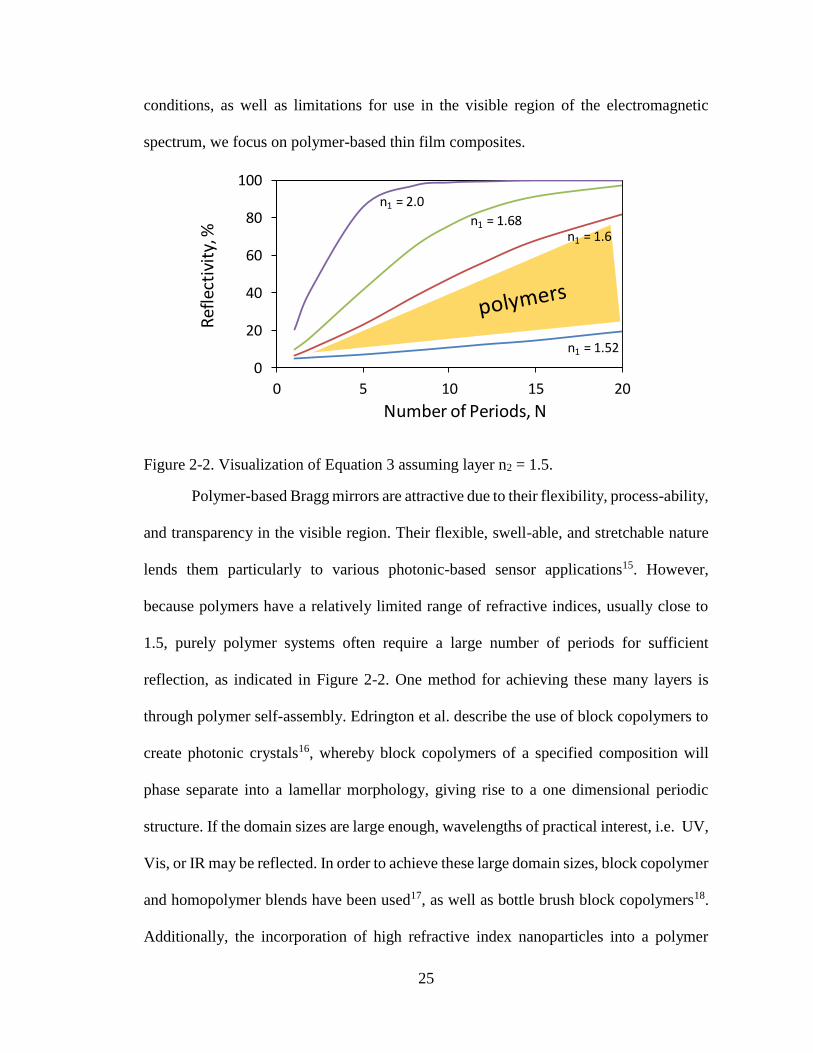
spectrum, we focus on polymer-based thin film composites.
Figure 2-2. Visualization of Equation 3 assuming layer n2 = 1.5.
Polymer-based Bragg mirrors are attractive due to their flexibility, process-ability,
and transparency in the visible region. Their flexible, swell-able, and stretchable nature
lends them particularly to various photonic-based sensor applications15. However,
because polymers have a relatively limited range of refractive indices, usually close to
1.5, purely polymer systems often require a large number of periods for sufficient
reflection, as indicated in Figure 2-2. One method for achieving these many layers is
through polymer self-assembly. Edrington et al. describe the use of block copolymers to
create photonic crystals16, whereby block copolymers of a specified composition will
phase separate into a lamellar morphology, giving rise to a one dimensional periodic
structure. If the domain sizes are large enough, wavelengths of practical interest, i.e. UV,
Vis, or IR may be reflected. In order to achieve these large domain sizes, block copolymer
and homopolymer blends have been used17, as well as bottle brush block copolymers18.
Additionally, the incorporation of high refractive index nanoparticles into a polymer
0
20
40
60
80
100
0 5 10 15 20
Ref
lect
ivit
y, %
Number of Periods, N
n1 = 1.52
n1 = 1.68
n1 = 2.0
n1 = 1.6

26
matrix provides another way to achieve sufficient reflection for photonic applications19,20.
Miguez et al. describe a unique method for creating polymer-infiltrated nanoparticle
layers, resulting in highly reflecting, flexible 1DPCs with 6 periods, however strain tuning
properties of these materials were not reported21. Kolle et al. demonstrates the concept of
stretch-tunable 1DPCs using a purely polymer system22. In this work we utilize the
advantage offered by nanoparticles in reducing the number of periods required for
significant reflection, as well as those of using an elastic polymer host, to create flexible
and stretchable nanocomposite tunable 1DPCs.
Recently, polymer-based one and three dimensional photonic crystals have been
used to fabricate mechanochromic sensors, or sensors that respond to an external
mechanical stimulus with a variation in color. Typical values of sensitivity, defined as the
shift in the wavelength of peak reflectance divided by the applied strain (nm/%), for these
sensors ranges from 0.7 to 5.3, and are dependent on the type of force applied and the
material systems23. Additionally, much of the focus is on photonic gels, as gels have
exhibited higher sensitivities23,24 Gels, however, rely on solvent-induced swelling; in this
work, we choose to use elastomer-based sensors which are suitable for diverse
environments that would be unsuitable for solvent-dependent gel sensors.
Specifically, we demonstrate the use of highly filled elastomer nanocomposites
for use in stretchable photonic applications. The structure of the Slide-Ring elastomers
chosen for this work is shown in Figure 2-3, and consists of cyclodextrin molecules which
have been functionalized for UV-crosslinking and threaded onto poly(ethylene glycol)
chains. The polymer chains are connected topologically by figure-of-eight crosslinks and
are freely moveable. The moveable cyclodextrin crosslinks allow for distribution of stress
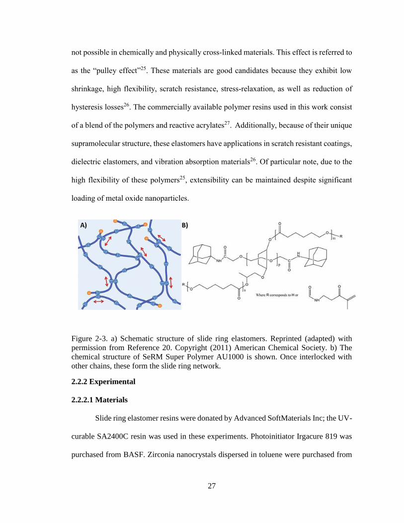
27
not possible in chemically and physically cross-linked materials. This effect is referred to
as the “pulley effect”25. These materials are good candidates because they exhibit low
shrinkage, high flexibility, scratch resistance, stress-relaxation, as well as reduction of
hysteresis losses26. The commercially available polymer resins used in this work consist
of a blend of the polymers and reactive acrylates27. Additionally, because of their unique
supramolecular structure, these elastomers have applications in scratch resistant coatings,
dielectric elastomers, and vibration absorption materials26. Of particular note, due to the
high flexibility of these polymers25, extensibility can be maintained despite significant
loading of metal oxide nanoparticles.
Figure 2-3. a) Schematic structure of slide ring elastomers. Reprinted (adapted) with
permission from Reference 20. Copyright (2011) American Chemical Society. b) The
chemical structure of SeRM Super Polymer AU1000 is shown. Once interlocked with
other chains, these form the slide ring network.
2.2.2 Experimental
2.2.2.1 Materials
Slide ring elastomer resins were donated by Advanced SoftMaterials Inc; the UV-
curable SA2400C resin was used in these experiments. Photoinitiator Irgacure 819 was
purchased from BASF. Zirconia nanocrystals dispersed in toluene were purchased from

28
Pixelligent. Polyvinyl Alcohol (PVOH, Mowiol 4-88) was purchased from Sigma
Aldrich. 89,000 MW polystyrene-block-poly(ethylene-ran-butylene)-block-polystyrene
(SEBS) was purchased from Sigma Aldrich.
2.2.2.2 Preparation of 1DPCs
1DPCs were fabricated by sequential stacking of multiple bilayers as shown in
Figure 2-3. For each bilayer, a water-soluble sacrificial layer was coated onto a silicon
wafer using 5 wt% PVOH in water onto a silicon wafer at 3000 rpm for one minute. The
PVOH layer was then baked at 110 oC for one minute to evaporate residual water. For the
high refractive index layer, ZrO2 was added to a 2.5 wt% SA2400C toluene solution to
achieve a 70% ZrO2 solution (with respect to total weight of solids). 1 wt% (with respect
to the weight of SA2400C) of Irgacure 819 was added from a 5 wt% photoinitiator
solution. This solution was mixed and exposure to light was minimized. For the low
refractive index layer, a 5 wt% solution of SA2400C and 1 wt% Irgacure 819 in toluene
was used. The nanoparticle-filled layer was spin coated onto the PVOH layer at 5000 rpm
for 20 seconds and then UV-cured using OAI UV light source with emission peak at 365
nm and intensity of 17 mJ/cm2. Following the cure, the unfilled polymer solution was
spin coated at 3000 rpm for 20 seconds and then cured. This was repeated on 6 substrates
simultaneously, in order to minimize any time variation of the polymer-nanoparticle
solutions and to make sure the bilayers thicknesses were consistent. The substrates were
placed top down onto an approximately 150-micron thick transparent SEBS
thermoplastic elastomer substrate. Elastomer substrates were prepared by blade coating
from 20 wt% solutions in toluene. Water was pipetted around the perimeter of the silicon
substrate and covered to keep undisturbed for one hour. After an hour, the PVOH layer

29
had dissolved, leaving the bilayer film in contact with the elastic substrate. This process
was repeated for each bilayer to build a 6 bilayer 1DPC.
Figure 2-4. Schematic demonstrating fabrication of high-low index bilayers.
2.2.2.3 Characterization
An aluminum frame was designed to hold and stretch the 1DPC while taking
reflectance measurements, as shown in Figure 2-4. Two translation stages (Altos
Photonics) were attached to an aluminum plate opposite each other, with the 1DPC
secured between them. Using a Filmetrics F20, baseline measurements were taken using
a silicon wafer and then reflectance measurements of the 1DPC were taken while the film
was unstrained and at various strain percentages. Changes in length across the 10 by 17
mm 1DPC were measured using digital calipers and used to calculate strain.
UV
Water soluble layer
High index layer
Low index layerH2O release

30
Figure 2-5. a) Photograph of straining plate under Filmetrics F40, b) photograph of
straining plate, and c) illustration of film before and after strain is applied.
2.2.3 Results and Discussion
2.2.3.1 ZrO2-Slide Ring Composite Film Properties
Well dispersed ZrO2 nanocrystals were mixed with UV-curable Slide-Ring
elastomer resins and a photoinitiator in a toluene solution. Solutions were spin cast and
the proper film thicknesses were achieved by controlling the spin coating rpm and the
weight percent of polymer and nanoparticles in solution. In order to determine the
suitability of the nanoparticles for optical applications, the transparency of the composites
was considered. Transmittance measurements were taken for composites containing 70
wt% ZrO2. Due to the layered nature of the final structure, transmittance measurements
were taken of five layers of composite material that had been consecutively spin coated
and UV-cured. The transmittance spectrum, shown in Figure 2-5a, indicated excellent
transparency of the composites. The layered films retained transparency above 94% in
a. b.
c.

31
the visible spectrum. This transparency, even at a high loading of particles, arose from
the nanoparticles’ small size and good dispersability within the polymer host. The
nanoparticles, with average diameters centered at 6 nm, were small enough to avoid
scattering of incident light. The TEM image in Figure 2-5b shows results consistent with
the supplier (diameter 6 nm). Additionally, no aggregation is observed which would lead
to scattering. The TEM sample was prepared by floating a composite film directly onto a
copper grid.
Figure 2-6. a) Transmission spectra of 5 layers of 70 wt% ZrO2 in UV-cured slide ring
elastomer and b) TEM image of ZrO2 nanoparticles dispersed within a slide ring
elastomer matrix at 70 wt% nanoparticles. Scale bar is 80 nm.
The refractive index of the materials was measured over the visible spectrum for
various weight percentages of ZrO2 in the elastomer matrix. By incorporating high
80nm
0
20
40
60
80
100
400 500 600 700 800
% T
ran
smit
tan
ce
Wavelength, nm
a.
b.

32
refractive index nanoparticles, we show that the composite refractive index can be
increased, resulting in good refractive index contrast for the 1DPCs. Figure 2-6a shows
refractive index as a function of weight and volume percent of ZrO2. The refractive index
increased linearly with increasing nanoparticle volume percent, as expected.19 The
refractive index at 70 wt% (30 vol%) was 1.68. This provided a refractive index
difference of 0.18.
2.2.3.2 1DPC Fabrication and Charcterization
1DPCs were fabricated by spin coating and UV-curing layers of filled and unfilled
elastomer resins, forming bilayers. These bilayers were lifted and stacked on each other
by using a water-soluble sacrificial base layer. The SEM image in Figure 2-6b shows an
example of a 5 bilayer 1DPC coated directly above a water-soluble sacrificial layer, all
on top of a silicon wafer. Figure 2-6b shows a 1DPC, fabricated by spin coating each
layer directly on top of the pervious without lifting and stacking individual bilayers (see
Experimental). The increased electron scattering caused by the nanoparticles in the filled
layers gave rise to the brighter appearance of the high-index layers. 1DPCs with
thicknesses designed to reflect in the red region of the visible spectrum were fabricated
according to the following criteria:
𝜆0/4 = 𝑛𝐻𝑡𝐻 = 𝑛𝐿𝑡𝐿, (4)
where the optical thicknesses of the high index layer and low index layer are equal to
each other as well as to one fourth of the wavelength to be reflected. Appropriate
rotational speeds and concentrations of solutions were used in order to achieve the desired
thicknesses via spin coating (see Experimental).

33
Figure 2-7. a) Refractive index of various nanocomposite compositions and b) SEM
image of a 5 bilayer 1DPC consisting of alternating filled (70 wt% ZrO2) and unfilled
Slide-Ring elastomers. The bottom-most layer is a water-soluble sacrificial layer of
polyvinyl alcohol on silicon.
Film thickness was determined by variable angle spectroscopic ellipsometry and
was used to measure simultaneously, the individual thicknesses of the water-soluble
polymer layer, the ZrO2-filled elastomer layer, and the unfilled elastomer layer. The
change in phase and amplitude of the incident polarized light were measured by the
ellipsometer and then fit to a Cauchy model to determine thickness. The thicknesses
measured from this method were 110 nm and 121 nm for the filled and unfilled layers,
respectively, with an expected variation in film thickness on the order of 5 nm. Figure 2-
7 shows the expected variation in film thickness for films fabricated via spin coating. The
1.45
1.5
1.55
1.6
1.65
1.7
1.75
0 20 40 60 80
Ref
ract
ive
Inde
x
ZrO2 Content, %
Volume %
Weight %
2 um
a.
b.

34
samples used for the figure were 5 wt% PVOH in water, which was used as the water-
soluble sacrificial layer for the 1DPC sensor fabrication. The thicknesses of each sample
were measured by variable angle spectroscopic ellipsometry and have approximately 4
nm or error associated with their measured thicknesses.
Figure 2-8. Film thicknesses from spin coated films. The error between sample
thicknesses are 4.02, 4.1, and 4.4 nm, respectively. The overall standard deviation of the
film thicknesses is 1.6 nm.
Using the Filmetrics simulation software, which uses the complex matrix form of
the Fresnel equations, we obtained the reflectance response for a 6-bilayer Bragg mirror.
The model consisted of 6 periods of high (1.67) and low (1.5) refractive index layers of
110 and 121 nm, respectively, on a 1.5 index substrate. The refractive index and thickness
values were obtained from ellipsometry measurements. The calculated results (bandwidth
and intensity) match very well with the experimental results of our unstrained 6-bilayer
1DPC (Figure 2-8), confirming the accuracy of the layer thicknesses and refractive index
values, as well distinct boundaries between the high and low index layers.

35
Figure 2-9. Simulated and experimental reflectance spectrum for 70 wt% ZrO2 composite
1DPCs containing 6 periods.
2.2.3.3 Sensor Behavior
In order to measure the response of the 1DPC to strain, a simple stretching device
was constructed to fit beneath the reflectometer in order to take measurements as strain
was applied to the film. All measurements were taken at 90o relative to the sample surface
with strain varying from 0 to 42%. Figure 2-9a and b show the shift in wavelength of
peak reflectance as strain is applied. The reflectance peak shifts to shorter wavelengths
as strain on the film is increased. The applied tensile strain corresponds to compression
in the direction normal to the plane of the applied strain, causing the thickness to decrease,
thereby blue-shifting the reflectance peak in accordance with Equation 1 (Figure 2-9a, b).
The color of the 1DPCs visibly changes from red to blue as the film is stretched, as shown
in Figure 2-9c. Though measurements were taken at 90o, photographs were taken in a
broadly lit room and the angle was chosen in order to best convey the color observed
0
0.1
0.2
0.3
0.4
0.5
0.6
400 500 600 700 800 900 1000
Wavelength, nm
Ref
lect
ance
Experiment
Simulation

36
under 90o incident light. Some discoloration is observed, particularly near the edges of
the 10 by 17 mm film due to defects resulting from handling and fabrication, however the
color in the center area (of at least 50 mm2) of the sensor remains consistent.
Figure 2-10. a) Reflectance spectra of a 6 period 1DPC under increasing strain (0 to 42%),
b) peak reflected wavelength as a function of strain, and c) digital photographs of 6-layer
1DPC under increasing strain from 0% (red) to approximately 40% (blue).
Mechanochromic sensitivity, defined as peak shift per percent strain, provides a
useful metric for characterizing various sensor material systems.15 While the highest
reported sensitivity is 12 nm/% for a lamellar block copolymer system in compression,
the mechanochromic sensitivity of block copolymer gels in uniaxial tension ranged in
magnitude from 0.7 to 5.25 nm/%.28 As shown in Table 2-1, the 1DPCs reported here
demonstrate a maximum 36mechanochromic sensitivity as large at -6.05 nm/% for
uniaxial tension. However, though the magnitude of the initial sensitivity is 6.05 nm/%,
the value decreased after the sensor was left strained over several months (see Figure 2-
Increasing strain
0
0.1
0.2
0.3
0.4
0.5
0.6
400 500 600 700 800 900 1000
Ref
lect
ance
Wavelength, nm
Increasing strain
400
500
600
700
800
0 0.1 0.2 0.3 0.4 0.5
Peak
Wav
ele
ngt
h
Strain
cycle 1cycle 2cycle 3cycle 4
a.
c.
b.
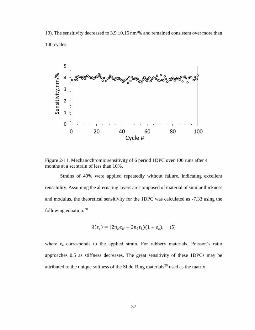
37
10). The sensitivity decreased to 3.9 ±0.16 nm/% and remained consistent over more than
100 cycles.
Figure 2-11. Mechanochromic sensitivity of 6 period 1DPC over 100 runs after 4
months at a set strain of less than 10%.
Strains of 40% were applied repeatedly without failure, indicating excellent
reusability. Assuming the alternating layers are composed of material of similar thickness
and modulus, the theoretical sensitivity for the 1DPC was calculated as -7.33 using the
following equation:28
𝜆(𝜀𝑧) = (2𝑛𝐻𝑡𝐻 + 2𝑛𝐿𝑡𝐿)(1 + 𝜀𝑧), (5)
where εz corresponds to the applied strain. For rubbery materials, Poisson’s ratio
approaches 0.5 as stiffness decreases. The great sensitivity of these 1DPCs may be
attributed to the unique softness of the Slide-Ring materials29 used as the matrix.
0
1
2
3
4
5
0 20 40 60 80 100
Sen
siti
vity
, nm
/%
Cycle #

38
Table 2-1. 1DPC Mechanochromic Sensitivity
Run Δεmax, % Δλ, nm Sensitivity, Δλ/Δεmax
1 43.3 -261 -6.05 2 43.2 -238 -5.57 3 42.5 -234 -5.52 4 42.5 -224 -5.26
100 runs averaged 39.3±1.7 -153±3.4 -3.9±0.16
2.2.4 Conclusions
We have demonstrated the use of polymer/nanoparticle composite materials for
unique optical sensor materials. The refractive index of polymer materials was modified
by incorporating high refractive index nanoparticles, thus reducing the number of layers
required to generate sufficient reflection. The use of UV-curable slide ring elastomers as
the matrix allowed for high loadings of 6 nm ZrO2 nanoparticles to be incorporated into
the matrix while maintaining transparency, flexibility, and extensibility. These composite
materials were used to construct strain-tunable 1DPCs, comprised of just 6 periods, which
exhibited reflectance above 40% and maximum mechanochromic sensitivity of over 6
nm/% strain.
2.3 Gradient Photonic Materials
2.3.1 Background
Many optical phenomena in nature like the reflecting color of butterfly30 or beetle
wings31, peacock feathers32, or chameleon skin33 are based on photonic crystals. The
remarkable color shift of chameleon skin is based on excitation of guanine nanocrystals
embedded in dermal iridophores, which allows chameleons to rapidly change their skin
color.

39
The principle of photonic crystals was discovered by John and Yablanovitch in
the late 1980s9,10. Since this time, photonic crystals found broad applications in light
emitting diodes4, photovoltaics34, lasers35 and sensors36. One-dimensional photonic
crystals (1DPCs) are materials which manipulate the flow of light through a photonic
bandgap (or stop band). Within the bandgap a certain range of wavelengths is forbidden
from propagating through the medium, analogous to the way semiconductors bandgaps
exclude electrons. 1DPCs, which are also sometimes referred to as Bragg mirrors, consist
of alternating layers of high and low refractive index layers results in enhanced reflection
due to constructive interference. Optical properties of 1DPCs depend on the refractive
index contrast, the number and thickness of layers, and the incident angle. The thickness
and therefore the reflectance of certain wavelength can be tuned via the strain, as
described in the previous chapter. There we showed a reflectance blue-shift with
increasing applied strain37.
A further natural principle are gradient materials which can be observed e.g. in
sea mussels38. Their mussel byssus threads are longitudinal soft-hard gradient materials
which connect the soft mussel interior to a hard surface like a stone39. Biomimicking such
materials provides materials with excellent mechanical properties e.g. in stiffness40–43.
Here, we demonstrate the preparation and use of photonic gradient materials. A
1DPC with a uniform composition over the whole area is attached to an elastomer with a
stiffness (modulus) gradient. The unstrained composite shows a consistent reflectance
over the whole surface. Application of a strain leads to thinner layers, resulting in a
reflected color shift to smaller values. The intensity of the color shift is correlated to the

40
layer thickness which is directly related to the magnitude of strain, which is dependent
on modulus.
The refractive index layers were prepared from slide-ring elastomers which were
filled with functionalized ZrO2 nanocrystals. Zirconium dioxide is well known to enhance
the refractive index of materials. The small ZrO2 nanocrystals can be dispersed very well
in the slide-ring elastomer matrix. Slide-ring elastomers consist of cyclodextrins which
are arranged along polyethylene glycol chains25. The cyclodextrin rings are freely
movable along the polymer chain. Application of a strain leads to a very homogeneous
stress distribution within the material, since all crosslinks can be adjusted very well
regarding their local load. This effect is also known as pulley-effect. The 1DPC consists
of six high and five low refractive index layers which alternate periodically. The high
refractive index layers consist of slide-ring elastomer which is filled with ZrO2
nanocrystals. The low refractive index layer consists only of the slide-ring elastomer
without nanocrystals37.
2.3.2 Experimental
2.3.2.1 Materials
Slide ring elastomer resin, SA2400C, was donated by Advanced SoftMaterials
Inc. Photoinitiator Irgacure 819 was purchased from BASF. Zirconia nanocrystals
dispersed in toluene were purchased from Pixelligent. Polyvinyl Alcohol (PVOH,
Mowiol 4-88) was purchased from Sigma Aldrich. PDMS elastomer resin Sylgard 184
was purchased from Dow Corning.

41
2.3.2.2 Preparation of Gradient Photonic Material
Two types of gradient modulus PDMS strips were fabricated using PDMS
elastomer resin Sylgard 184: a linear modulus gradient strip and an oscillating modulus
gradient strip. For the PDMS strip with linear gradient in modulus from one end to the
other, the soft end was prepared with a Sylgard 184 mixing ratio of base to curing agent
of 25:1, while the ratio at the hard end had a mixing ratio of 10:1. The oscillating modulus
gradient sample was prepared using a curing ratio of 50:1 for the soft regions and 5:1 for
the hard regions. The 6 cm oscillating modulus strip has 1.5 cm hard regions at the ends
and 1 cm soft-hard-soft regions in the middle. Glass syringes with these two components
were mounted on a high-precision syringe pump system (Cetoni neMESYS). The
syringes were connected via PVC tubing to a custom-made mixing head with an attached
disposable static mixer. Mixing of both components is controlled via a flow profile. The
compositional gradient was extruded into a Teflon mold (dimension: 60 mm x 10 mm x
2 mm) which is attached to a linear motion slide. The samples were cured at room
temperature overnight and then post-cured at 80°C for two hours.
1DPCs were prepared on PDMS via sequential stacking of multiple bilayers
following the general procedure described elsewhere37. First, a sacrificial layer of
polyvinyl alcohol (5 wt% in water) was first spin coated on a silicon wafer (3000 rpm, 1
min) and baked at 110 °C to remove residual water. High and low index layers were spin
coated and cured sequentially, building a 5.5 period structure. All solutions and
dispersions were prepared using toluene as a solvent. The solution for the high refractive
index layer was prepared by mixing ZrO2 nanocrystal dispersion in toluene with slide-
ring elastomer SA2400C in a solids ratio of 70/30 ZrO2 to SA2400C. Total solids

42
concentration was 5 wt% and the solution was spin coated for 20 seconds at 1700 rpm.
For the low refractive index solution, no ZrO2 was added. Total solids concentration was
4 wt% and the solution was spin coated at 2700 rpm for 20 seconds. For both solutions,
1 wt% photoinitiator Irgacure 819 with respect to SA2400C was added, filtered, and
stored in the dark.
1DPCs are prepared on a silicon wafer and then transferred to PDMS via film
transfer. PDMS is treated with O2 plasma to activate/hydrophilize the surface. Activated
PDMS and the 1DPC on silicon are placed in a Petri dish and immersed in water. After
dissolution of the sacrificial PVOH layer, the 1DPC separates from the wafer, floats on
water, and can be transferred to the PDMS surface. The floating medium is drained, and
the sample is dried with compressed nitrogen.
2.3.2.3 Characterization
For visualization of the gradient, UV-Vis absorption was measured with an
Analytik Jena reader FLASH Scan 530. A red fluorescent dye (CAS-Nr. 123174-58-3,
Kremer Pigments, Germany) was added at 0.02 wt% to the soft PDMS component. Cured
samples were measured on a 384-well microplate. The distance between each measuring
spot was 4.7 mm. UV-Vis Spectra were recorded between 375 and 900 nm and set to zero
at 650 nm for comparison. The reported values for the absorption maxima at 560 nm were
determined from 4 equally prepared samples (each sample was measured twice) and
averaged.
Mechanical characterization was conducted on a DMTA. Disk-like specimens
were cut out of the sample in defined distances. Compression was tested.
43
Film thickness and refractive index measurements were done using a JA Woollam
RC2 Ellipsometer. Ellipsometric data was fit using the Cauchy model, for transparent
films, from 400 to 1700 nm.
Reflectance measurements on gradient refractive index materials were conducted
using a Filmetrics F40. A special stage was used to strain the sample to defined values.
Strain values were determined via a digital caliper. After recording a baseline with a
silicon calibration wafer, reflectance measurements were conducted at defined strains and
defined positions. For each strain and position, three measurements were conducted.
Reflectance spectra were normalized before plotting.
2.3.3 Results and Discussion
2.3.3.1 Gradient PDMS
Two types of gradient modulus PDMS strips were fabricated. First a PDMS strip
with linear gradient in modulus from one end to the other. The soft end was prepared
from Sylgard 184 with a mixing ratio of base to curing agent of 25:1, while the ratio at
the hard end had a mixing ratio of 10:1, resulting in a linear modulus gradient ranging
from 0.3 MPa at the soft end to 0.9 MPa at the hard end42. The PDMS strip with an
oscillating modulus gradient consists of a hard-soft-hard-soft-hard pattern. The soft
regions were prepared from Sylgard 184 with a mixing ratio of base to curing agent of
50:1, while the ratio at the hard end had a mixing ratio of 5:1, resulting in an oscillating
modulus gradient. Representative mechanical and UV-Vis absorption data can be found
in previously published reports39,42.

44
2.3.3.2 Optical Response: Linear Modulus Gradient
After attaching the 1DPC film to the linear gradient strip, reflectance
measurements were taken (in the unstrained state) at five locations along the length of the
sample, as shown in Figure 2-12a. The uniformity of reflectance behavior is clearly
observed from the corresponding photograph shown in Figure 2-12b as well as the
measured reflectance spectra shown in Figure 2-12c. The reflectance peak of the 5.5
period 1DPC is located at 618±5 nm, corresponding to a reddish-orange color. The
unstrained reflectance spectrum was modeled using the Filmetrics F40 software which
calculates spectra according to the complex matrix form of the Fresnel equations. The
modeled 5.5 period 1DPC consisted of alternating 1.67 and 1.5 refractive index layers of
thicknesses 92 and 102 nm, as measured by ellipsometry. The calculated reflectance peak
location and bandwidth matches well with the experimental results, as shown in Figure
2-12c.

45
Figure 2-12. Schematic (a) and photograph (b) of unstrained 1DPC on linear gradient
PDMS strip and c) normalized reflectance of unstrained linear gradient 1DPC.
The 1DPC on PDMS was then strained in 10% increments until 20% and then
strained in 5% increments. Reflectance measurements were recorded at the same five
locations along with PDMS strip, as indicated in Figure 2-13a. The measurement
locations are no longer equally spaced, as in the unstrained sample, due to the modulus
gradient leading to a strain gradient. At 30% strain (with respect to the length of the strip),
the PDMS broke and no more measurements were able to be obtained. At 25% strain, the
sample displays a gradient in reflectance from a greenish-blue to yellowish-orange, as
observed in the photograph in Figure 2-13b. The normalized reflectance spectra in Figure
2-13c clearly show the effect of the modulus gradient of the PDMS substrate. Here, the
reflectance peak at the soft end (indicated in blue) experiences the greatest blue-shift (92
nm), while the reflectance peak at the hard end experiences only a 38 nm blue-shift
compared to the unstrained sample. These results are aligned with what is expected due
to the dependence of strain on modulus.
0
0.1
0.2
0.3
0.4
0.5
0.6
0.7
0.8
0.9
1
400 500 600 700 800
No
rmal
ized
Ref
lect
ance
Wavelength, nm
1B (soft end)2B3B4B5B (hard end)Model
hard endsoft end
1 2 3 4 5a. b.
c.

46
Figure 2-13. Schematic (a) and photograph (b) of strained (25%) 1DPC on linear
gradient PDMS strip and c) normalized reflectance of strained linear gradient 1DPC
(25%).
2.3.3.3 Optical Response: Oscillating Modulus Gradient
The same optical measurements were carried out using an oscillating modulus
gradient PDMS sample. The modulus oscillates between “soft” and “hard” in the
following manner: hard-soft-hard-soft-hard. A 1DPC 5.5 period film with the same
refractive indices and thicknesses as in the previous sample was affixed to the PDMS
strip and in the unstrained state, small marks were made every 0.5 cm from the one end
to the other to indicate the location for measurements throughout the straining experiment
(Figure 2-14a). Due to the more complex fabrication of the oscillating modulus gradient
PDMS strip, the thickness of the strip is not as uniform as the linear modulus gradient
sample, as can be from the visual appearance in the unstrained sample (Figure 2-14b,
top). The oscillating modulus gradient sample was subjected to strain in 5% increments
(with respect to the length of the strip), up to 30%, at which point the PDMS failed. At
soft end
1 2 3 4 5
0
0.1
0.2
0.3
0.4
0.5
0.6
0.7
0.8
0.9
1
400 500 600 700 800
No
rmal
ized
Ref
lect
ance
Wavelength, nm
1B (soft end)2B3B4B5B (hard end)
hard end
a. b.
c.

47
25% strain, the effect of the oscillating modulus gradient PDMS substrate can be clearly
observed visually, as shown in the photographs in Figure 2-14b. Here, the observed colors
change from a uniform reddish-orange in the unstrained state to a striped effect in which
the colors oscillate between yellowish-orange to blue. The peak locations along the
unstrained and 25% strained sample are compared in Figure 2-14c. As observed in the
linear modulus gradient sample, the “hard” sections of the oscillating modulus gradient
experience the smallest blue-shift, while the “soft” regions experience a greater blue-shift.
Again, due to the more complex fabrication of the oscillating modulus gradient PDMS,
the reflectance in the 25% strained sample are as uniform and consistent in variation as
would be expected from a perfectly fabricated sample. Nonetheless, an oscillation in the
magnitude of the blue-shift is clearly evident.
Figure 2-14. Schematic (a) and photograph (b) of strained (25%) 1DPC on oscillating
gradient PDMS strip and c) normalized reflectance of strained oscillating gradient
1DPC (25%).
1 2 3 4 5
500
520
540
560
580
600
620
640
0 1 2 3 4 5 6
Max
imu
m o
f ref
lect
ance
pea
k (n
m)
Position (cm)
unstrained
strained
unstrained gradient (0%)
strained gradient (25%)
a. b.
c.
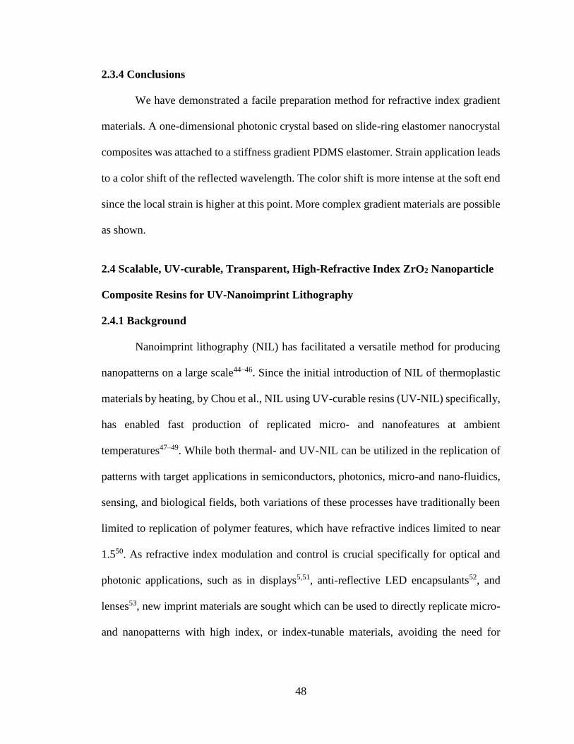
48
2.3.4 Conclusions
We have demonstrated a facile preparation method for refractive index gradient
materials. A one-dimensional photonic crystal based on slide-ring elastomer nanocrystal
composites was attached to a stiffness gradient PDMS elastomer. Strain application leads
to a color shift of the reflected wavelength. The color shift is more intense at the soft end
since the local strain is higher at this point. More complex gradient materials are possible
as shown.
2.4 Scalable, UV-curable, Transparent, High-Refractive Index ZrO2 Nanoparticle
Composite Resins for UV-Nanoimprint Lithography
2.4.1 Background
Nanoimprint lithography (NIL) has facilitated a versatile method for producing
nanopatterns on a large scale44–46. Since the initial introduction of NIL of thermoplastic
materials by heating, by Chou et al., NIL using UV-curable resins (UV-NIL) specifically,
has enabled fast production of replicated micro- and nanofeatures at ambient
temperatures47–49. While both thermal- and UV-NIL can be utilized in the replication of
patterns with target applications in semiconductors, photonics, micro-and nano-fluidics,
sensing, and biological fields, both variations of these processes have traditionally been
limited to replication of polymer features, which have refractive indices limited to near
1.550. As refractive index modulation and control is crucial specifically for optical and
photonic applications, such as in displays5,51, anti-reflective LED encapsulants52, and
lenses53, new imprint materials are sought which can be used to directly replicate micro-
and nanopatterns with high index, or index-tunable materials, avoiding the need for

49
typical, subsequent process steps of etching patterned polymers and depositing high-
index materials.
Several different approaches to increasing the refractive index of polymers have
been reported. For example, much work has focused on the synthetic design of high
refractive index polymers, which involves incorporating substituents with high atomic
refractions such as aromatic rings and halogen and sulfur atoms. For example, refractive
index modulation from 1.68 to 1.79 has been demonstrated by varying the sulfur and
aromatic content of polyimides54,55. Though a high index can be achieved using this
method, and with conjugated polymers the index reaches up to 2.7, these polymers often
suffer from low solubility, high optical dispersion, and low optical transparency, making
them poor candidates for many optical applications56. Another approach involves adding
high refractive index, inorganic nanoparticles within a polymer matrix. High index
materials such as crystalline TiO2, ZrO2, and amorphous silicon are commonly used, as
they are transparent in the visible region. Nanoparticles must be smaller than 40 nm and
well-dispersed throughout the matrix to maintain optical transparency57,58. In 2014,
Beaulieu et al. demonstrated nanoimprinting of a TiO2 nanoparticle/UV-resin composite
where control over refractive index was achieved from 1.58 to 1.91 (λ=800 nm)20. This
approach, however, requires the use of significant quantities of volatile solvents, limiting
its potential for large-scale applications. In addition, the use of TiO2 in polymeric
composites, particularly for light-based applications, raises concerns about the
photocatalytic properties of TiO2.
In this work we combine two methods in order to increase the refractive index of
UV-curable resins: the addition of ZrO2 nanoparticles to an acrylic UV-resin, as well as

50
to a mixture of UV-resin and the high refractive index small molecule, N-vinylcarbazole
(NVC). The resulting material is UV-curable and solvent-free, making it an attractive
composite for scaling to large scale production, such as roll-to-roll.
2.4.2 Experimental
2.4.2.1 Materials
Monomer resin Miramer 1142 (M1142) was provided by Miwon Specialty
Chemical Co. Ltd. Zirconium Dioxide (ZrO2) nanoparticle dispersion (50 wt% in
propylene glycol monomethyl ether acetate) was purchased from Pixelligent
Technologies LLC. The photoinitiators Irgacure TPO-L and Esacure KL200 were
provided by BASF and Lamberti, respectively. Propylene glycol monomethyl ether
(PGMEA) and N-vinylcarbazole (NVC) were purchased from Sigma Aldrich. All
materials were used without further purification.
2.3.2.2 Preparation of Composites
M1142 and ZrO2 composites were prepared by mixing the liquid resin with the
nanoparticle dispersion in varying concentrations. Mixtures of M1142 with 0 to 30 vol%
ZrO2 were prepared (with respect to total solids). Mixtures were prepared in glass dishes,
placed on a magnetic stir/hot plate at 65oC, and left overnight. Mass loss was monitored
to ensure the removal of all PGMEA from the ZrO2 dispersion. M1142/NVC composites
were prepared by mixing solid NVC with M1142 resin in various ratios in glass vials,
which were then stirred and heated above the melting point of NVC (65oC) until the NVC
was melted and dispersed into the M1142 resin. These M1142/NVC mixtures were then
used to prepare M1142/NVC/ZrO2 composites the same way the M1142/ZrO2 composites

51
were prepared. 3% of either TPO-L or KL200 photoinitiator was added after solvent
removal.
2.4.2.3 Preparation of Nanopatterned and Smooth Films
To prepare patterned films, composite mixtures were pipetted onto an anti-
adhesion treated silicon stamp and covered with a piece of ST505 PET film. A roller was
used to evenly spread the resin, and the resins were then cured under 365 nm UV light
for about one minute. Smooth, thin films (< 500 nm) were prepared for ellipsometry
measurements by diluting the different composite mixtures with PGMEA to 10 wt% (with
respect to all solids). These solutions were then spin coated onto silicon wafers and cured
under nitrogen. 150 µm films for UV-Vis spectroscopy were prepared by pressing resin
between two glass slides separated by a 150 µm cover slip. One glass slide was treated
with an anti-adhesion layer for easy removal after curing.
2.4.2.4 Preparation of Roll to Roll Stamps
To test the scalability of the composite resin, PDMS stamps backed on a release
liner were prepared as shown in Figure 2-15. First, an aluminum mastering plate was
designed to accommodate 18 1in2 square masters (Figure 2-15a, b). This design allows
for testing of many interchangeable test patterns, as well as testing the imprint/release
direction. The square masters are held securely by vacuum (see Figure 2-15d) and PDMS
stamps can be prepared by pouring PDMS over the masters and curing in the presence of
a silicone release liner. Once cured (2 days at room temperature), the liner and masters
can be separated by peeling and the stamp-containing liner can be affixed to the NIL drum
(Figure 2-15c). The roll-to roll (R2R) process for UV-NIL, shown in Figure 2-15d,
involves a PET web (1) which is first plasma treated (2) to activate the surface to promote

52
good wetting/adhesion of the resin to the substrate, coated with the resin with a gravure
coater (3), then the resin is contacted with the stamp and exposed to UV at the UV-NIL
state (4).
Figure 2-15. Schematic of aluminum mastering plate with 1in2 slots for masters(a),
mastering plate fitted with diverse test patterns on 1 in2 substrates for stamp preparation
(b), test pattern stamp wrapped around drum (c), photograph of mastering plate with
vacuum connections (d), and photograph of R2R UV-NIL with PET web (1), plasma
treatment (2), gravure coater (3), and UV-NIL stage (4).
2.4.2.5 Characterization
The refractive index (nD) at λ = 589 nm (sodium D-line) of uncured composite
resins was measured using an ATAGO NAR-1T refractometer. Films were cured using
365 nm UV light with ca. 1 mW/cm2 from a biostep® USDT-20ML-8R source. Imprinted
patterns were imaged using an Olympus BX51 optical microscope. UV-Vis spectra were
obtained using a Perkin Elmer Lambda 900 UV/VIS/NIR-spectrometer. The refractive
index of cured films was obtained using a JA Woollam RC2 variable angle spectroscopic
ellipsometer. Ellipsometric data from 55-75o was fit using the Cauchy model in the
CompleteEase software. Height profiles of patterned films were obtained using a Zygo
Nexview Optical Profiler.
a. b. c.
d. e.

53
2.4.3 Results and Discussion
2.4.3.1 High Index Composite Components and Refractive Index
Miramer 1142 (M1142) is a commercially available monomer resin with a
relatively high refractive index (nD=1.578) and was therefore chosen as the matrix/base
component of our high index composites. The high refractive index of M1142 arises from
its chemical structure which possesses aromatic rings, as shown in Figure 2-16a. In order
to further increase the matrix refractive index, we also selected the small molecule N-
vinylcarbazole (NVC). NVC also possesses aromatic rings (Figure 2-16b) which give rise
to an elevated refractive index (nD= 1.68).
Figure 2-16. Chemical structure of a) M1142 (o-phenylphenol ethyl acrylate) and b) N-
vinylcarbazole.
Zirconium dioxide (ZrO2) nanoparticles (NPs) were added to and dispersed in
M1142 in order to further increase the refractive index. After adding the ZrO2 NPs (up to
30 vol% with respect to total solids) and removing solvent, the composite resins
maintained their transparency and no aggregation was visible by visual inspection. This
indicates a good dispersion, which is a result of the compatibility of the ZrO2 capping
agents and M1142. Further indication of a good dispersion is evident in the linear increase
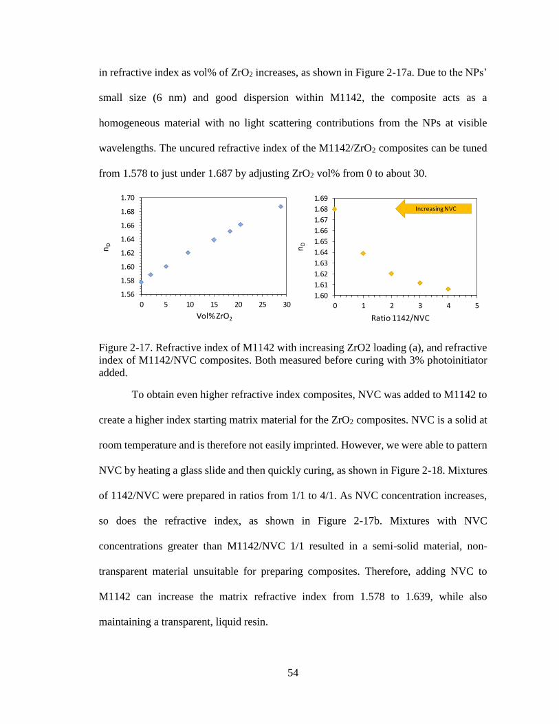
54
in refractive index as vol% of ZrO2 increases, as shown in Figure 2-17a. Due to the NPs’
small size (6 nm) and good dispersion within M1142, the composite acts as a
homogeneous material with no light scattering contributions from the NPs at visible
wavelengths. The uncured refractive index of the M1142/ZrO2 composites can be tuned
from 1.578 to just under 1.687 by adjusting ZrO2 vol% from 0 to about 30.
Figure 2-17. Refractive index of M1142 with increasing ZrO2 loading (a), and refractive
index of M1142/NVC composites. Both measured before curing with 3% photoinitiator
added.
To obtain even higher refractive index composites, NVC was added to M1142 to
create a higher index starting matrix material for the ZrO2 composites. NVC is a solid at
room temperature and is therefore not easily imprinted. However, we were able to pattern
NVC by heating a glass slide and then quickly curing, as shown in Figure 2-18. Mixtures
of 1142/NVC were prepared in ratios from 1/1 to 4/1. As NVC concentration increases,
so does the refractive index, as shown in Figure 2-17b. Mixtures with NVC
concentrations greater than M1142/NVC 1/1 resulted in a semi-solid material, non-
transparent material unsuitable for preparing composites. Therefore, adding NVC to
M1142 can increase the matrix refractive index from 1.578 to 1.639, while also
maintaining a transparent, liquid resin.
1.60
1.61
1.62
1.63
1.64
1.65
1.66
1.67
1.68
1.69
0 1 2 3 4 5n
D
Ratio 1142/NVC
Increasing NVC
1.56
1.58
1.60
1.62
1.64
1.66
1.68
1.70
0 5 10 15 20 25 30
nD
Vol% ZrO2
55
Figure 2-18. NVC on glass. Scale bar is 20 µm.
Composites containing ZrO2 loadings between 0 and 30 vol% were prepared using
the M1142/NVC matrix mixtures. As demonstrated in Figure 2-19a, the refractive index
of the starting material is increased due to addition of NVC. As the concentration of ZrO2
increases, the refractive index is also increased, and we note that for M1142/NVC 2/1
with 30 vol% ZrO2, we can achieve an index above 1.7 for uncured composites. We do
note that though the M1142/NVC 1/1 mixture has the highest starting index, at 30 vol%
ZrO2 loading, the index is less than that of the 30 vol% M1142/NVC 2/1 sample. This
result is due to agglomeration of the additives, which is confirmed by the milky
appearance of the 30 vol% ZrO2 M1142/NVC 1/1 composite resin. As higher
concentrations of NVC are added, the mixture viscosity increases which may inhibit the
dispersability of the NPs. The M1142/NVC 1/1 mixture with 30 vol% ZrO2 has an
approximately equal refractive index value with M1142/NVC 4/1 and 8/3.2.5 with 30
vol% ZrO2. Mixtures of M1142/NVC 4/1 with ZrO2 loading at 30 vol% were stable and
clear, and resulting in a refractive index of 1.6991. Due to the effect of increasing
viscosity with increasing NVC, the M1142/NVC 4/1 30 vol% ZrO2 composite was
56
selected as the optimal mixture. Figure 2-19b shows the refractive indices of the cured
composite resins, which is slightly higher than the uncured samples due to volume
reduction during polymerization. M1142/NVC 4/1 with 30 vol% ZrO2 maintains a
refractive index above 1.7 over the whole visible spectrum with nD, cured = 1.726. The
UV-Vis spectra in Figure 2-19c show that 150 µm films of various composite mixtures
maintain good transparency over the visible spectrum. Pure NVC films result in the
lowest transmittance values, while the M1142/NVC 4/1 with 30 vol% ZrO2 possesses
transparency above 85% in the visible region.

57
Figure 2-19. Refractive index (λ = 589 nm) of M1142/NVC compositions with increasing
ZrO2 loading (a), refractive index versus wavelength of cured films of various
compositions (b), and UV-Vis spectra of various cured 150 µm films (c).
2.4.3.2 Batch Imprinting of Resins
1.55
1.60
1.65
1.70
1.75
1.80
350 550 750 950 1150 1350
Ref
ract
ive
Ind
ex
Wavelength, nm
M1142/30% ZrO2
M1142
M1142/NVC
4/1/30% ZrO2
0
20
40
60
80
100
300 400 500 600 700
Tran
smit
tan
ce, %
Wavelength, nm
1142/NVC 1/1
1142/NVC 4/1
NVC
1142/NVC 4/1 30%ZrO2
1.60
1.62
1.64
1.66
1.68
1.70
1.72
0 10 20 30 40
nD
Vol% ZrO2
1142/NVC 4/1
1142/NVC 8/3.25
1142/NVC 2/1
1142/NVC 1/1
a.
b.
c.

58
These high refractive index resins were imprinted using a master mold with
several different patterns and dimensions. As seen in the optical microscope images in
Figure 2-20, there is no discernable difference between the M1142 only and the increased
index M1142/NVC (8/3.25) with 30 vol% ZrO2 resins.
Figure 2-20. Imprints of M1142 with a) 0 vol% ZrO2 and b) 30 vol% ZrO2 and Imprints
of M1142/NVC 8/3.25 with c) 0% ZrO2 and d) 30 vol% ZrO2 Scale bars are 20 µm.
Height profiles were also examined, and as shown in Figure 2-21. Both M1142 and
M1142/30 vol% ZrO2 imprinted patterns have heights of 400 nm, indicating that these
high index composite resins can be used to faithfully transfer nanopatterns.
M1142 M1142/30ZrO2
M1142/NVC 8/3.25 M1142/NVC 8/3.25/30ZrO2

59
Figure 2-21. Height profiles of imprinted M1142 (a, b) and height profiles of imprinted
M1142/30 vol% ZrO2 (c, d).
2.4.3.3 Roll to Roll Demonstrations
Large-scale imprinting demonstrations are currently underway.
2.3.4 Conclusions
By controlling the composition of the Miramer composite resins using high-
refractive index nanoparticles and small molecules, the refractive index of the UV-
curable resin could be increase from 1.58 to 1.73. By mixing the nanoparticle dispersion
into the resin, or resin-NVC mixture, and then evaporating the solvent, we were able to
achieve a homogeneous, transparent, solvent-free UV-curable material. Using UV-NIL,
the high index resins were successfully patterned using stamps with critical dimensions
of 400 nm. Imprinted patterns were highly uniform over the patterned area and feature
M1142
M1142/30ZrO2

60
dimensions were consistent between different resin compositions. This solvent-free, high
refractive index material is well suited for large-scale, roll-to-roll processing of patterned
optical structures.
2.5 Conclusions
We have formulated two high-refractive index composite systems based on UV-
curable resins and ZrO2 nanocrystals. The first system uses the novel Slide-ring elastomer
UV-curable resin whose unique topologically crosslinked structure allows for distribution
of stresses and therefore high strains. Combined with up to 30 vol% ZrO2 nanocrystals,
these composite films had a refractive index of 1.67 at 589 nm. The refractive index
contrast between the NP-filled and unfilled elastomer allowed for fabrication of a
visually-vibrant 1DPC with reflectance peaks in the visible region, consisting of just 5-6
bilayers. When strained up to 42% the 1DPC demonstrated a reflectance blue-shift of
more than 200 nm, changing in color from red to blue.
The same Slide-ring elastomer/ZrO2 NP system was used to fabricate novel
gradient reflectance materials. Taking inspiration from nature, these gradient materials
demonstrate modulus-dependent reflectance responses when strained. Linear modulus
gradient samples exhibited an increased blue-shift in reflectance peak from the hard to
the soft end. The oscillating modulus gradient samples exhibited similar behavior in the
hard and soft regions, resulting in a striped appearance.
Finally, the aforementioned system was adapted for UV-NIL of high refractive
index polymer/NP composite resins. Resin Miramer 1142 was selected for its relatively
high refractive index (1.58) and ZrO2 dispersed in PGMEA was added up to 30 vol%.
The resulting composite resin had a cured refractive index of 1.71. When small molecule
61
NVC was added, the 30 vol% ZrO2 composites reached a cured index of 1.73. Composite
resins were adapted for large-scale imprinting and therefore contained no solvent.
Samples were imprinted and UV-cured, resulting in good feature replication for all
compositions.
2.6 References
(1) Li, C.; Colella, N. S.; Watkins, J. J. Low-Temperature Fabrication of
Mesoporous Titanium Dioxide Thin Films with Tunable Refractive Indices for
One-Dimensional Photonic Crystals and Sensors on Rigid and Flexible
Substrates. ACS Appl. Mater. Interfaces 2015, 7 (24), 13180–13188.
(2) Brongersma, M. L.; Cui, Y.; Fan, S. Light Management for Photovoltaics Using
High-Index Nanostructures. Nat. Mater. 2014, 13 (5), 451–460.
(3) Loncar, M.; Doll, T.; Vuckovic, J.; Scherer, A. Design and Fabrication of Silicon
Photonic Crystal Optical Waveguides. J. Light. Technol. 2000, 18 (10), 1402–
1411.
(4) Wierer, J. J.; David, A.; Megens, M. M. III-Nitride Photonic-Crystal Light-
Emitting Diodes with High Extraction Efficiency. Nat. Photonics 2009, 3 (3),
163–169.
(5) Nakamura, T.; Fujii, H.; Juni, N.; Tsutsumi, N. Enhanced Coupling of Light from
Organic Electroluminescent Device Using Diffusive Particle Dispersed High
Refractive Index Resin Substrate. Opt. Rev. 2006, 13 (2), 104–110.
(6) Matsuda, T.; Funae, Y.; Yoshida, M.; Yamamoto, T.; Takaya, T. Optical
Material of High Refractive Index Resin Composed of Sulfur-Containing
Aromatic Methacrylates. J. Appl. Polym. Sci. 2000, 76, 50–54.
(7) Arbabi, A.; Horie, Y.; Bagheri, M.; Faraon, A. Dielectric Metasurfaces for
Complete Control of Phase and Polarization with Subwavelength Spatial
Resolution and High Transmission. Nat. Nanotechnol. 2015, 10 (11), 937–943.
(8) Baets, R. Microphotonics - Thin Films. Univ. Gent - Photonic Res. Gr.
(9) John, S. Strong Localization of Photons in Certain Disordered Dielectric
Superlattices. Phys. Rev. Lett. 1987, 58 (23), 2486–2489.
(10) Yablonovitch, E. Inhibited Spontaneous Emission in Solid-State Physics and
Electronics. Phys. Rev. Lett. 1987, 58 (20), 2059–2062.

62
(11) Hunt, N. E. J.; Schubert, E. F.; Logan, R. A.; Zydzik, G. J. Enhanced Spectral
Power Density and Reduced Linewidth at 1.3 Μm in an InGaAsP Quantum Well
Resonant-Cavity Light-Emitting Diode. Appl. Phys. Lett. 1992, 61 (19), 2287–
2289.
(12) Colodrero, S.; Mihi, A.; Haggman, L.; Ocana, M.; Boschloo, G.; Hagfeldt, A.;
Miguez, H. Porous One-Dimensional Photonic Crystals Improve the Power-
Conversion Efficiency of Dye-Sensitized Solar Cells. Adv. Mater. 2009, 21 (7),
764–770.
(13) Calvez, S.; Hastie, J. E.; Guina, M.; Okhotnikov, O. G.; Dawson, M. D.
Semiconductor Disk Lasers for the Generation of Visible and Ultraviolet
Radiation. Laser Photonics Rev. 2009, 3 (5), 407–434.
(14) Chiappelli, M. C.; Hayward, R. C. Photonic Multilayer Sensors from Photo-
Crosslinkable Polymer Films. Adv. Mater. 2012, 24 (45), 6100–6104.
(15) Lee, J. H.; Koh, C. Y.; Singer, J. P.; Jeon, S. J.; Maldovan, M.; Stein, O.;
Thomas, E. L. 25th Anniversary Article: Ordered Polymer Structures for the
Engineering of Photons and Phonons. Adv. Mater. 2014, 26 (4), 532–569.
(16) Edrington, A. C.; Urbas, A. M.; Derege, P.; Chen, C. X.; Swager, T. M.;
Hadjichristidis, N.; Xenidou, M.; Fetters, L. J.; Joannopoulos, J. D.; Fink, Y.;
Thomas, E. L. Polymer-Based Photonic Crystals. Adv. Mater. 2001, 13 (6), 421–
425.
(17) Urbas, A.; Sharp, R.; Fink, Y.; Thomas, E. L.; Xenidou, M.; Fetters, L. J.
Tunable Block Copolymer/homopolymer Photonic Crystals. Adv. Mater. 2000,
12 (11), 812–814.
(18) Sveinbjornsson, B. R.; Weitekamp, R. a.; Miyake, G. M.; Xia, Y.; Atwater, H. a.;
Grubbs, R. H. Rapid Self-Assembly of Brush Block Copolymers to Photonic
Crystals. Proc. Natl. Acad. Sci. 2012, 109 (36), 14332–14336.
(19) Caseri, W. Nanocomposites of Polymers and Metals or Semiconductors:
Historical Background and Optical Properties. Macromol. Rapid Commun. 2000,
21 (11), 705–722.
(20) Beaulieu, M. R.; Hendricks, N. R.; Watkins, J. J. Large-Area Printing of Optical
Gratings and 3D Photonic Crystals Using Solution-Processable
Nanoparticle/Polymer Composites. ACS Photonics 2014, 1 (9), 799–805.
(21) Calvo, M. E.; Miguez, H. Flexible, Adhesive, and Biocompatible Bragg Mirrors
Based on Polydimethylsiloxane Infiltrated Nanoparticle Multilayers. Chem.
Mater. 2010, 22 (13), 3909–3915.

63
(22) Kolle, M.; Zheng, B.; Gibbons, N.; Baumberg, J. J.; Steiner, U. Stretch-Tuneable
Dielectric Mirrors and Optical Microcavities. Opt. Express 2010, 18 (5), 4356–
4364.
(23) Chan, E. P.; Walish, J. J.; Urbas, A. M.; Thomas, E. L. Mechanochromic
Photonic Gels. Adv. Mater. 2013, 25 (29), 3934–3947.
(24) Yue, Y.; Kurokawa, T.; Haque, M. A.; Nakajima, T.; Nonoyama, T.; Li, X.;
Kajiwara, I.; Gong, J. P. Mechano-Actuated Ultrafast Full-Colour Switching in
Layered Photonic Hydrogels. Nat. Commun. 2014, 5, 4659.
(25) Ito, K. Slide-Ring Materials Using Topological Supramolecular Architecture.
Curr. Opin. Solid State Mater. Sci. 2010, 14 (2), 28–34.
(26) Noda, Y.; Hayashi, Y.; Ito, K. From Topological Gels to Slide-Ring Materials. J.
Appl. Polym. Sci. 2014, 131 (15), 1–9.
(27) Araki, J.; Ito, K. Recent Advances in the Preparation of Cyclodextrin-Based
Polyrotaxanes and Their Applications to Soft Materials. Soft Matter 2007, 3 (12),
1456.
(28) Chan, E. P.; Walish, J. J.; Thomas, E. L.; Stafford, C. M. Block Copolymer
Photonic Gel for Mechanochromic Sensing. Adv. Mater. 2011, 23 (40), 4702–
4706.
(29) Ito, K. Novel Entropic Elasticity of Polymeric Materials: Why Is Slide-Ring Gel
so Soft? Polym. J. 2012, 44 (1), 38–41.
(30) Biró, L. P.; Bálint, Z.; Kertész, K.; Vértesy, Z.; Márk, G. I.; Horváth, Z. E.;
Balázs, J.; Méhn, D.; Kiricsi, I.; Lousse, V.; Vigneron, J. P. Role of Photonic-
Crystal-Type Structures in the Thermal Regulation of a Lycaenid Butterfly Sister
Species Pair. Phys. Rev. E - Stat. Physics, Plasmas, Fluids, Relat. Interdiscip.
Top. 2003, 67 (2), 7.
(31) Sun, J.; Bhushan, B. Structure and Mechanical Properties of Beetle Wings: A
Review. RSC Adv. 2012, 2 (33), 12606.
(32) Zi, J.; Yu, X.; Li, Y.; Hu, X.; Xu, C.; Wang, X.; Liu, X.; Fu, R. Coloration
Strategies in Peacock Feathers. Proc. Natl. Acad. Sci. 2003, 100 (22), 12576–
12578.
(33) Teyssier, J.; Saenko, S. V.; Van Der Marel, D.; Milinkovitch, M. C. Photonic
Crystals Cause Active Colour Change in Chameleons. Nat. Commun. 2015, 6, 1–
7.
(34) Chutinan, A.; Kherani, N. P.; Zukotynski, S. High-Efficiency Photonic Crystal
Solar Cell Architecture. Opt. Express 2009, 17 (11), 8871–8878.

64
(35) Park, H.-G.; Kim, S.-H.; Kwon, S.-H.; Ju, Y.-G.; Yang, J.-K.; Baek, J.-H.; Kim,
S.-B.; Lee, Y.-H. Electrically Driven Single-Cell Photonic Crystal Laser. Science
(80-. ). 2004, 305 (5689), 1444–1447.
(36) Chow, E.; Grot, a; Mirkarimi, L. W.; Sigalas, M.; Girolami, G. Ultracompact
Biochemical Sensor Built with Two-Dimensional Photonic Crystal Microcavity.
Opt. Lett. 2004, 29 (10), 1093–1095.
(37) Howell, I. R.; Li, C.; Colella, N. S.; Ito, K.; Watkins, J. J. Strain-Tunable One
Dimensional Photonic Crystals Based on Zirconium Dioxide/slide-Ring
Elastomer Nanocomposites for Mechanochromic Sensing. ACS Appl. Mater.
Interfaces 2015, 7 (6), 3641–3646.
(38) Waite, J. H.; Lichtenegger, H. C.; Stucky, G. D.; Hansma, P. Exploring
Molecular and Mechanical Gradients in Structural Bioscaffolds. Biochemistry
2004, 43 (24), 7653–7662.
(39) Claussen, K. U.; Giesa, R.; Scheibel, T.; Schmidt, H. W. Learning from Nature:
Synthesis and Characterization of Longitudinal Polymer Gradient Materials
Inspired by Mussel Byssus Threads. Macromol. Rapid Commun. 2012, 33 (3),
206–211.
(40) Claussen, K. U.; Giesa, R.; Schmidt, H. W. Longitudinal Polymer Gradient
Materials Based on Crosslinked Polymers. Polym. (United Kingdom) 2014, 55
(1), 29–38.
(41) Claussen, K. U.; Lintz, E. S.; Giesa, R.; Schmidt, H. W.; Scheibel, T. Protein
Gradient Films of Fibroin and Gelatine. Macromol. Biosci. 2013, 13 (10), 1396–
1403.
(42) Claussen, K. U.; Scheibel, T.; Schmidt, H. W.; Giesa, R. Polymer Gradient
Materials: Can Nature Teach Us New Tricks? Macromol. Mater. Eng. 2012, 297
(10), 938–957.
(43) Claussen, K. U.; Tebbe, M.; Giesa, R.; Schweikart, A.; Fery, A.; Schmidt, H.-W.
Towards Tailored Topography: Facile Preparation of Surface-Wrinkled Gradient
Poly(dimethyl Siloxane) with Continuously Changing Wavelength. RSC Adv.
2012, 2 (27), 10185.
(44) Chou, S. Y.; Krauss, P. R.; Renstrom, P. J. Imprint of Sub-25 Nm Vias and
Trenches in Polymers. Appl. Phys. Lett. 1995, 67 (1995), 3114.
(45) John, J.; Tang, Y.; Rothstein, J. P.; Watkins, J. J.; Carter, K. R. Large-Area,
Continuous Roll-to-Roll Nanoimprinting with PFPE Composite Molds.
Nanotechnology 2013, 24 (50), 505307.

65
(46) Leitgeb, M.; Nees, D.; Ruttloff, S.; Palfinger, U.; G??tz, J.; Liska, R.; Belegratis,
M. R.; Stadlober, B. Multilength Scale Patterning of Functional Layers by Roll-
to-Roll Ultraviolet-Light-Assisted Nanoimprint Lithography. ACS Nano 2016, 10
(5), 4926–4941.
(47) Thesen, M. W.; Nees, D.; Ruttloff, S.; Rumler, M.; Rommel, M.; Schlachter, F.;
Grützner, S.; Vogler, M.; Schleunitz, A.; Grützner, G. Inkjetable and Photo-
Curable Resists for Large-Area and High-Throughput Roll-to-Roll Nanoimprint
Lithography. J. Micro/Nanolithography, MEMS, MOEMS 2014, 13 (4), 43003.
(48) Haisma, J. Mold-Assisted Nanolithography: A Process for Reliable Pattern
Replication. J. Vac. Sci. Technol. B Microelectron. Nanom. Struct. 1996, 14 (6),
4124.
(49) Chang, C. Y.; Yang, S. Y.; Chu, M. H. Rapid Fabrication of Ultraviolet-Cured
Polymer Microlens Arrays by Soft Roller Stamping Process. Microelectron. Eng.
2007, 84 (2), 355–361.
(50) Brandrup, J.; Immergut, E. H.; Grulke, E. A.; Abe, A.; Bloch, D. R. Polymer
Handbook, 4th Ed.; John Wiley & Sons: New York, 2005.
(51) Kitamura, K.; Okada, K.; Fujita, N.; Nagasaka, Y.; Minoru, U.; Sekimoto, Y.;
Kurata, Y. Fabrication Method of Double-Microlens Array Using Self-Alignment
Technology. Jpn. J. Appl. Phys. 2004, 43 (8B), 5840–5844.
(52) Krogman, K. C.; Druffel, T.; Sunkara, M. K. Anti-Reflective Optical Coatings
Incorporating Nanoparticles. Nanotechnology 2005, 16, S338–S343.
(53) Suwa, M.; Niwa, H.; Tomikawa, M. High Refractive Index Positive Tone Photo-
Sensitive Coating. J. Photopolym. Sci. Technol. 2006, 19 (2), 275–276.
(54) Liu, J.; Nakamura, Y.; Ogura, T.; Shibasaki, Y.; Ando, S.; Ueda, M. Optically
Transparent Sulfur-Containing Polyimide - TiO 2 Nanocomposite Films with
High Refractive Index and Negative Pattern Formation from Poly ( Amic Acid ) -
TiO 2 Nanocomposite Film. 2008, No. 6, 273–281.
(55) You, N.; Suzuki, Y.; Yorifuji, D.; Ando, S.; Ueda, M. Synthesis of High
Refractive Index Polyimides Derived from and Aromatic Dianhydrides. 2008,
6361–6366.
(56) Higashihara, T.; Ueda, M. Recent Progress in High Refractive Index Polymers.
Macromolecules. 2015, pp 1915–1929.
(57) Caseri, W. INORGANIC NANOPARTICLES AS OPTICALLY EFFECTIVE
ADDITIVES FOR POLYMERS. Chem. Eng. Commun. 2009, 196, 549–572.

66
(58) Yuwono, A. H.; Liu, B.; Xue, J.; Wang, J.; Elim, H. I.; Ji, W.; Li, Y.; White, T. J.
Controlling the Crystallinity and Nonlinear Optical Properties of Transparent
TiO2 – PMMA Nanohybrids. J. Mater. Chem. 2004, 14, 2978–2987.

67
CHAPTER 3
FABRICATION OF PLASMONIC TIN NANOSTRUCTURES BY
NITRIDATION OF NANOIMPRINTED TIO2 NANOPARTICLES
3.1 Introduction
Metamaterials and plasmonics have generated intense interest due for diverse
applications in areas such as structural color1, sensing2–4, energy storage5, sub-diffraction
imaging6,7, light concentration8, cloaking9, negative refraction10, and optical information
storage11. The expansion of research in these fields can be attributed in part to advances
in nanoscale fabrication techniques including well-controlled nanoparticle synthesis12
and lithography techniques13–15. Carefully designed arrays of metal nanoparticles or
nanostructures give rise to plasmonic resonances that can be harnessed for sensing.
Despite many advances in fabrication, the primary materials used in plasmonic
applications have remained gold and silver. Although these noble metals have many
advantages such as the well-studied and controllable synthesis of gold nanoparticles,
there are some inherent disadvantages to using these metals that hinder their usefulness
in practical plasmonic devices. Gold and silver are expensive and not chemically and/or
thermally stable under harsh conditions, which limits their range of practical applications.
Additionally, the optical characteristics (dielectric function) of gold and silver are fixed,
again limiting the scope of more varied applications. Due to these acknowledged
disadvantages, researchers have sought alternative materials16–18. Despite their previous
demonstration as plasmonic materials19–21, transition metal nitrides, such as titanium
nitride (TiN), have continued to receive attention due to the growing demand for
plasmonic materials. TiN specifically has been proposed as alternative plasmonic

68
materials due to its very high melting point, chemical stability, tunable dielectric function,
and fabrication methods compatible with existing manufacturing techniques22,23. For
example, researchers have shown the superior stability of electron beam-patterned TiN
nanostructures compared to noble metals like gold24.
Commonly used fabrication methods for TiN films and structures include reactive
sputtering22, chemical vapor deposition25, atomic layer deposition26, and pulsed laser
deposition27. In order to fabricate TiN in many different patterns and geometries,
researchers have explored the nitridation of titanium dioxide (TiO2) to fabricate TiN28–33.
The nitridation reaction between ammonia and TiO2 occurs at high temperatures
(~1000oC). At these temperatures, ammonia breaks down into hydrogen and nitrogen gas,
the former facilitates the creation of oxygen vacancies, and the latter then fills the
vacancies. Moon et al. showed that the conversion of hollow spheres of TiO2 to TiN
occurs at 800oC, and can be used for electrochemical storage32. Zukalova et al. also
demonstrated the successful conversion of electrospun TiO2 fibers to TiN and TiOxNy
using temperatures up to 1000oC31. The recent publication from Guler et al. demonstrates
the nitridation of TiO2 nanorods and nanowires by electron beam lithography and TiO2
deposition34.
In this work we use a scalable, solvent-assisted soft nanoimprint lithography
(NIL) method to quickly generate large areas of nanopatterned crystalline TiO2 surfaces
and structures, as demonstrated in previous publications in our group35,36. The direct
patterning of NPs by soft NIL is especially attractive as this method does not require
expensive, time consuming processes such as EBL (aside from initial master fabrication).
This form of NIL uses PDMS stamps, many of which can be produced from one silicon

69
master, and each of which can be reused many times, minimizing costs. The area of
imprinted structures is thus primarily limited by only the size of the original patterned
master. Feature sizes down of 100 nm can be easily replicated using PDMS, however for
smaller, high aspect ratio features, variations of PDMS with higher modulus values are
required37,38. High aspect ratio, small, high-density patterning has been demonstrated
using PDMS-based NIL with organic resists and sol-gel materials. Compatible, mature
NIL processing tools targeting high volume production, which utilize PDMS-based
stamps are beginning to reach the market38. We believe our specific method, in which we
directly pattern crystalline inorganic materials using NP dispersions 36, which leads
directly to strong, functional patterned surfaces, provides an attractive alternative to the
traditional NIL of organic resists and sol-gel materials. By then subjecting these patterned
and planar TiO2 films to heated ammonia, nanopatterned TiN surfaces and structures are
obtained. We analyze the resulting chemical and optical characteristics of the planar and
patterned films, as well as demonstrate the surface plasmon polariton (SPP) excitation via
grating coupling. This work is of particular interest as an attractive, low-cost, versatile,
and well-controlled fabrication method for nano-patterned, single and multilayer
plasmonic and metamaterial structures.
3.2 Experimental
3.2.1 Materials
TiO2 nanoparticles dispersed in 1,2-propanediol (20 wt%, anatase, 15 nm) were
purchased from US Research Nanomaterials, Inc. Poly(methyl methacrylate) (996k
molecular weight) was purchased from Sigma Aldrich, Titanium diisopropoxide
bis(acetylacetonate) (Ti(acac)2) (75 wt% in isopropanol) and reagent grade methanol,

70
isopropanol, toluene, and propylene glycol methyl ether acetate (PGMEA) were
purchased from Sigma Aldrich. Norland Optical Adhesive 60 (NOA60) was purchased
from Norland Products Inc. Sylgard 184 was purchased from Ellsworth Adhesives.
Compressed anhydrous ammonia (99.96 %) was purchased from Air Liquide. Silicon
wafers (p-type, B-doped, (100) orientation) were purchased from Nova Electronics and
quartz slides were purchased from Chemglass. Syringe filters were purchased from VWR
(PTFE, 0.45 µm). All materials were used without further purification.
3.2.2 Preparation of PDMS Stamps
Before PDMS stamp preparation, masters are fluorinated using (tridecafluoro-
1,1,2,2-tetrahydrooctyl)dimethylchlorosilane (FDMS). The silicon masters were soaked
in concentrated sulfuric acid overnight and then rinsed with water and IPA and then
subjected to O2 plasma for 5 minutes. The masters were then placed in a sealed desiccator
with approximately 75 mL of FDMS and left overnight at 75oC. After returning to room
temperature, the masters were removed, rinsed with IPA and water, and then ready for
stamp preparation.
PDMS stamps were prepared with Sylgard 184 using a base to curing agent weight
ratio of 1:10. The components were thoroughly mixed and then placed under vacuum for
approximately 10 minutes to degas. After degassing the uncured PDMS is poured into a
petri dish containing the face-up silicon masters. Any bubbles are eliminated and then the
petri dishes are placed in an oven at 75oC overnight. The stamps can be cut out of the
petri dishes with an X-acto knife and then peeled from the silicon masters.

71
3.2.3 Preparation of Nanoparticle-based Solutions
A 20-mL glass vial was charged with approximately 1 gram of 20 wt% TiO2
nanoparticles (NPs) in 1,2-propanediol. The NP dispersion was then diluted to either 2.5,
5, or 10 wt% by adding the appropriate amount of methanol. Approximately half a gram
of 75 wt% Ti(acac)2 sol-gel precursor (sol-gel) in isopropanol was added to another 20
mL vial and diluted to 2.5, 5, or 10 wt% using isopropanol. Both diluted dispersions were
sonicated for 5 minutes to ensure good mixing. Different ratio solutions of NP to sol-gel
were prepared by mixing different amounts of the two diluted solutions (100/0, 90/10,
80/20, 70/30, and 60/40 NP/sol-gel). These resulting solutions were sonicated and filtered
before use and remain stable for several months.
3.2.4 Preparation of Planar and Patterned TiO2 Nanoparticle-based Films
Silicon wafers and quartz slides were cut into approximately 1x1 in2 pieces. Planar
NP/sol-gel films were prepared by spin coating the different mixtures at 3000 rpm for 30
seconds. The films were then placed on a 50oC hotplate for 5 minutes to remove any
residual solvent. In order to prepare patterned films, the process in Figure 3-1a was
followed. The detailed process for fabricating NP-based patterns can be found in our
previous papers36. In short, the 2.5 wt% NP/sol-gel (100/0, 90/10, 70/30) solutions were
spin coated for 15 seconds. The still-wet film was then contacted with a PDMS stamp
containing nanofeatures. The substrate (with the stamp still in contact) was then moved
to the 50oC hotplate. After 5 minutes, the stamp was removed, leaving the transferred
nanopatterns. The resulting patterned area is scalable, limited only by the size of PDMS
stamps used, and is uniform over large areas, as shown in Figure 3-1b and c. For multi-
layer grid structures, the first imprinted layer was treated with oxygen plasma for 30

72
seconds and then planarized using 20 wt% NOA60 in PGMEA (cured under 254 nm UV).
After planarization, the process can be repeated by imprinting the second layer of lines
perpendicular to the first layer. The planarization and imprint procedure can be repeated
to build multilayer structures. To create an open grid, the organic planarization layer was
removed by calcining the entire structure at 750oC for 1 minute. All planar and patterned
samples were annealed in air at 500oC for two hours.
Figure 3-1. a) Fabrication method for patterned TiO2 and TiN films, b) cm-scale PDMS
stamps and imprinted gratings on silicon, and c) large-area SEM image of uniform,
defect-free, imprinted gratings.
3.2.5 Preparation of Perpendicular, Intersecting, TiO2 Bilayer Gratings
A slightly modified fabrication method can be adapted to prepare perpendicular
intersecting TiO2 bilayer gratings that are residual free, as outlined in Figure 3-2. The top
and bottom grating layers are designed to extend beyond the bilayer region in order to
allow for deposition of contacts for conductivity measurements (Figure 3-2g).

73
Figure 3-2. Schematic illustrating the process used to create intersecting, residual-layer-
free bilayer gratings by a) coating with PMMA, b) imprinting and PMMA lift-off, c)
planarizing, d) coating with PMMA, e) imprinting, f) PMMA lift off and calcination, g)
nitridation and electrode deposition.
First a silicon wafer is treated with oxygen plasma, and then spin coated with a 2%
PMMA solution in toluene. Half of the PMMA-coated wafer is then masked by a flat
piece of silicon and exposed with an OAI 1000-Watt DUV (254 nm) lamp for 180
seconds, then developed in PGMEA for 30 seconds, resulting in a half-PMMA-coated
silicon wafer (Figure 3-2a). TiO2 is then spin coated and imprinted following the
procedure described previously: a 2.5wt% TiO2 with 10% Ti(acac)2 (with respect to TiO2
NP weight) is spin coated for 10 seconds at 3000 rpm, the stamp is placed on top and then
it is dried on a hot plate at 50oC for 15 minutes (with a weight on top of the stamp). After
drying, the stamp is removed, and then the imprint is dipped in a beaker of sonicating
acetone, and dried with compressed nitrogen, revealing a clean silicon substrate on half
of the wafer (Figure 3-2b). Subsequently the entire substrate is planarized with NOA60
and the same PMMA procedure is carried out perpendicular to the first layer of imprinted
lines (Figure 3-2c-d). TiO2 is again imprinted, the PMMA is lifted off, and then the entire
sample is calcined, resulting in perpendicular, intersecting, residual-layer-free bilayer
Si PMMA
PMMA
a. b. c.
d. e. f. g.

74
gratings (Figure 3-2f, Figure 3-3a-c). The gratings can be nitrided following the
nitridation process described in the following section.
Figure 3-3. TiO2 intersecting residual-layer-free bilayer imprints at different
magnifications (a-c).
50 um
10 um
5 um
a.
b.
c.

75
3.2.6 Nitridation Process
TiO2 planar and patterned films were placed in a quartz process tube inside a tube
furnace. The tube was sealed and purged with nitrogen for 30 minutes. After purging, an
ammonia gas flow of 200 sccm was set and the furnace temperature was set to ramp up
to 1000oC over 4 hours, hold for 2, 4, or 6 hours, and then ramp down over 12 hours.
After cooling, the ammonia flow was stopped, and the samples were collected.
3.2.7 Characterization
X-ray diffraction (XRD) patterns were collected on a PANalitycal X'pert MPD-
PRO Bragg-Brentano θ-θ geometry diffractometer equipped with a secondary
monochromator over an angular range of 2θ = 8-80°. The Cu-Kα (λ = 0.15418 nm)
radiation was generated at 45 kV and 40 mA. Grazing incidence X-ray diffraction (XRD)
patterns were collected on a Brüker D8 Discover Bragg-Brentano theta-2theta geometry
diffractometer equipped with a Goebel mirror. Theta angles were fixed to 0.4, 0.5, 0.6,
0.8, 1.5° and a 2θ scan is performed over an angular range from 10 to 80°. Each
acquisition lasted for 10 hours. The Cu-Kα (λ = 0.15418 nm) radiation was generated at
45 KV and 40 mA. X-ray photoelectron spectroscopy (XPS) was performed using
Quantum 2000 Scanning ESCA microprobe (Physical Electronics, Inc.) with Al-Kα
radiation (1486.6 eV). Sputtering was done with Ar+ for 30 minutes, or until Si substrate
was reached. XPS data was analyzed using Multipak software version 9.3.0.3 from
Physical Electronics Inc. Scanning electron microscopy (SEM) and energy dispersive
electron microscopy (EDS) images were taken using a FEI Magellan FESEM. Elemental
mapping was done at 0.4 nA and 10 kV and images were collected for 220 seconds. Film
thicknesses and dielectric functions were determined by variable angle spectroscopic

76
ellipsometry (JA Woollam RC2). Ellipsometric data was collected from 50 to 70o and
was fit using the Cauchy and B-spline models in the CompleteEase software.
3.3 Results and Discussion
3.3.1 Planar Film Crystallinity and Composition
Several compositions of TiO2 NPs and TiO2 sol-gel precursors were used to create
TiO2 planar and patterned films. Films were prepared with NP to sol-gel precursor ratios
(by weight) of 100/0, 90/10, 80/20, 70/30 and 60/40. After annealing, the films were
treated with ammonia gas for 2, 4, or 6 hours (designated as a, b, or c). Numbers
associated with sample names refer to the nanoparticle concentration; those designated
“fto” and “ftn” correspond to the un-nitrided (oxide) and nitrided films, respectively.
Unless otherwise specified, we refer to the 100/0 samples.
Figure 3-4 shows the XRD patterns of un-nitrided and nitrided TiO2 films. The
100/0 and 90/10 sample XRD patterns before nitridation treatment (0 hr), shown in Figure
3-4a, clearly indicate the anatase phase of TiO2 with peaks appearing at 25 and 48o, while
the peaks at 22 and 33o are attributed to the silicon substrate. After the nitridation
treatment, a modification of the structure is observed; Figure 3-4a (2, 4, 6 hr) shows the
clear disappearance of the anatase peaks and the appearance of those corresponding to
TiN (osbornite) at 36 and 43o. Figure 3-4b shows low incidence scans done at several
grazing angles from 0.1 to 3o; contributions from the silicon substrate are evident from
50-60o. The low-angle scans of the treated films confirm the nitridation results from
Figure 3-4a, with nitrided samples showing no peaks corresponding to any TiO2 phase at
any angle. Additionally, no difference in peak position can be observed with variation of
grazing angle, indicating good homogeneity in the material structure. However, in these

77
low-angle scans of untreated TiO2, we can see the small contribution from the rutile
phase, which likely formed during the 500oC annealing step.
Figure 3-4. Standard XRD of a) TiO2 films before and after 2, 4, and 6-hour treatments,
and b) low incidence XRD of treated film from 0.1 to 3o.
20 30 40 50 60
0
20
Inte
nsity (
a.u
.)
()
3.0
2.5
2.0
1.5
1.0
0.8
0.6
0.5
0.4
0.3
0.2
0.1
20 30 40 50 60
0
50
100
150
200
250
300
350
400
450
500
Inte
nsity (
a.u
.)
()
FTN100-6h
FTN100-4h
FTN100-2h
FTN100-0h
FTN90-6h
FTN90-4h
FTN90-2h
FTN90-0h
a.
b.

78
We used XPS to extract additional information about the composition of the
treated films and chemical environment of elements composing the patterned films. XPS
allows more in-depth analysis of the resulting material, providing both the binding
energies of various elemental components and information about the atomic
concentration as a function of sputter time.
Figure 3-5. XPS data showing atomic concentration (AC) vs sputter time of different
elements for a) untreated TiO2, b) 2-hour ammonia treatment, c) 4-hour ammonia
treatment, and d) 6-hour ammonia treatment.
The XPS atomic concentration profiles in Figure 3-5 show the concentration of carbon,
titanium, silicon, nitrogen, and oxygen as a function of sputter time. We see in Figure 3-
5a that the untreated sample is virtually all titanium and oxygen in a 1:2 ratio, as expected
for TiO2. After 2, 4, and 6-hour treatments of 100% nanoparticle films, the oxygen
0
20
40
60
80
100
0 10 20 30
AC
, %
Sputter time, min
0 hr: TiO2 film
C1s Ti2p Si2p N1s O1s
0
20
40
60
80
100
0 10 20 30
AC
, %
Sputter time, min
4 hr
0
20
40
60
80
100
0 10 20 30A
C,%
Sputter time, min
2 hr
0
20
40
60
80
100
0 10 20 30
AC
, %
Sputter time, min
6 hr
a.
c.
b.
d.

79
concentration significantly decreases, while the nitrogen concentration is approximately
1:1 with the titanium concentration (Figure 3-5b-d). Additionally, we see that the 1:1 ratio
is maintained through the depth of the film, until reaching the substrate, noted by the
sharp increase in Si concentration. Remaining oxygen concentration in nitrided samples
(about 20% after 6-hour nitridation) may be due to the innate porosity of nanoparticle
films, as shown in Figure 3-7 and Table 3-1. Porosities shown in Table 3-1 were
calculated using the Lorentz-Lorenz equation (below).
𝑓2 =(𝐶 − 𝐴)
(𝐵 − 𝐴), 𝑣𝑜𝑙𝑢𝑚𝑒 𝑓𝑟𝑎𝑐𝑡𝑖𝑜𝑛 𝑐𝑜𝑚𝑝𝑜𝑛𝑒𝑛𝑡 2
𝐴 =(𝑛1
2−1)
(𝑛12+2)
, 𝐵 =(𝑛2
2−1)
(𝑛22+2)
, 𝐶 =(𝑛2−1)
(𝑛2+2)
Here, f2 is the volume fraction of air, n is the measured refractive index (Figure 3-6) and
n1 and n2 are the refractive indices of bulk TiO2 and air, respectively. using the measured
refractive indices.

80
Figure 3-6. Ellipsometric data of annealed TiO2 films fit using the Cauchy model.
Table 3-1. Heat treatments and calculated porosity of TiO2 films
Temperature, oC time (hr) n(λ=628.2) porosity, %
RT - 1.82 29.85
475 1 1.92 23.86
475 2hr 2 1.91 24.44
475 4hr 4 1.92 23.86
These pores effectively create increased surface area on which a native oxide layer may
form after nitridation treatment. Table 3-1 provides atomic concentration percentages,
and we can see that at longer treatment times, the concentration of nitrogen increases
slightly, and the oxygen concentration decreases. The observed saturation in nitrogen
concentration combined with the continued decrease in oxygen concentration is likely
due to decreasing surface area on which surface oxidation may take place, as a result of
longer treatment times. This is consistent with the results found by other researchers31.
Figure 3-7 compares TiO2 nanoparticle films untreated, annealed in air, and nitrided. The

81
visible change in porosity from the surface of the film implies some densification of the
films, which would result in lower surface area for oxidation.
Figure 3-7. a) TiO2 NP film heated at 475oC for 4 hours and b) after 6-hour nitridation
treatment (NH3, 1000oC). Scale bars are 1 µm.
The increase in Si noted in Table 3-2 could be a result of the diffusion of Si at high
temperatures, but is more likely due to film shrinkage, which results in small areas of
exposed substrate. This is in agreement with the former point, which stated that decreased
film thickness/film densification led to less surface oxidation.
Table 3-2. Atomic Concentrations (%) at 5 min sputter time
Ti N O C Si
TiO2* 31.1 0.8 65.9 1.6 0.6
2 hrs 34.1 33.2 29.1 0.3 3.25
4 hrs 33.3 37.2 19.2 1.9 8.4
6 hrs 39.2 39.8 12.1 0 8.8 (*TiO2 concentrations recorded at 10 min sputter time)
We also used XPS to examine the binding energies to elucidate the distinction
between TiO2, TiOxNy, and TiN in our resulting samples. After a 6-hour nitridation
treatment, we observe that the Ti2p and O1s peaks have shifted relative to those of the
untreated TiO2 NP film (Figure 3-8a, c). We additionally observe the appearance of the
N1s peak, as shown in Figure 3-8b. The Ti2p orbital is a split spin orbital and consists of

82
Ti2p1/2 and Ti2p3/2 peaks, which display different shapes and energies if the material
present is TiO2 or TiN. The Ti2p peaks of TiO2 have symmetric shapes, while the TiN
Ti2p peaks are known to have a complex shape including satellite shoulders, which leads
to difficulty in accurately fitting these peaks. The shift in Ti2p binding energy peaks also
provides insight into the sample composition. Literature reports binding energies of the
Ti2p3/2 orbital as: 458.1-458.3 eV for TiO2, 456.0-456.7 eV for TiOxNy, and 454.7-455.1
eV for TiN31,39. In Figure 3-8a, the Ti2p3/2 binding energy for our TiO2 NP reference
film is 458.8 eV and shifts to 454.6 eV after the 6-hour ammonia treatment, which
correspond to the expected energies reported for TiO2 and TiN, respectively. In addition
to the Ti2p3/2 binding energy peak shift, the TiN satellite shoulder becomes visible for
the nitrided samples. The shift in the Ti2p1/2 binding energy peak from 464 eV for TiO2
to 460 eV for the 6-hour treated sample is also indicative of the transition from TiO2 to
TiN. Despite the location of the Ti2p peaks being consistent with that of TiN, the peak
shapes are complex, possessing shoulders, making definitive peak assignments difficult
and consequently, the presence of other minor peaks associated with TiOxNy could be
embedded in the Ti2p region. The energy difference between the Ti2p split spin-orbit
components (Δ), Ti2p1/2 and Ti2p3/2, provides additional information about the sample.
For titanium metal, oxide, and nitride, Δ is reported as 6.1, 5.7 and 6.0 eV, respectively.
Δ for the untreated TiO2 NP film and the 6 hour binding energies (399-403 eV)29,31,39.
The O1s peak shifts from 530.2 to 531.6 eV after the 6-hour nitridation treatment, as well
as a dramatic reduction in the intensity, as shown in Figure 3-8c. The O1s peak associated
with TiO2 is reported at 530 eV, while that associated with TiOxNy should appear at 531.8
eV. The O1s peaks of the 6 hr ammonia treated sample shifts to 531.6 eV, consistent with

83
that of TiOxNy. To determine whether the O1s peak contains contributions from an
unreacted TiO2 phase, we fit the peaks of the 2 and 6 hr treated samples using multiple
bands, seen in Figure 3-8d-e. After 2 hours of treatment, the O1s peak cannot be
adequately fit with one band and is best fit with a large contribution at 530.8 eV and a
minor contribution at 532.7 eV. This could indicate the presence of TiO2 (530 eV) and
TiOxNy, despite TiO2 not appearing in the XRD analysis of treated samples. Others have
reported and attributed this result to either the formation of TiO2 on the surface after
treatment, or to amorphous TiO239. We also suggest that the small presence of rutile TiO2
picked up in some of the XRD patterns could be responsible, as rutile TiO2 may not
convert to TiN as readily as anatase TiO231. However, after 6 hours of treatment, the O1s
peak is best fit with a single band at 531.1 eV, indicating there are no longer any
significant TiO2 contributions. Additionally, the reduction in O1s intensity with treatment
time is consistent with the XPS atomic concentration results shown in Figure 3-5. The
surface of TiN is readily oxidized when exposed to the environment. Therefore, the
presence of oxygen throughout the thickness of the film is likely due to the nature of our
samples. Because our films are made from TiO2 nanoparticles, which initially contain up
to 30% porosity, this can result in an increased surface area which may be re-oxidized
after nitridation treatments. This is confirmed by XPS sputtering in Figure 3-5, which
indicates the presence of oxygen throughout the depth of the film. This increased sample
porosity and resulting surface oxidation could potentially be reduced by ripening the TiO2
NPs before nitridation treatment.
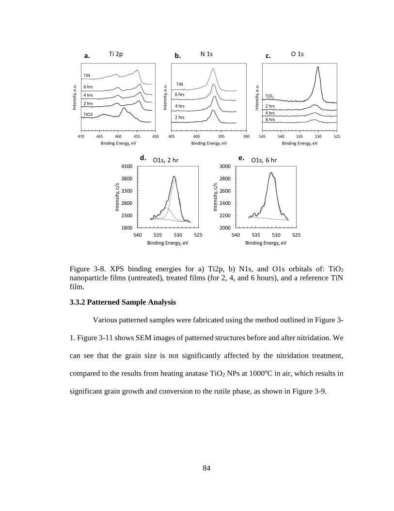
84
Figure 3-8. XPS binding energies for a) Ti2p, b) N1s, and O1s orbitals of: TiO2
nanoparticle films (untreated), treated films (for 2, 4, and 6 hours), and a reference TiN
film.
3.3.2 Patterned Sample Analysis
Various patterned samples were fabricated using the method outlined in Figure 3-
1. Figure 3-11 shows SEM images of patterned structures before and after nitridation. We
can see that the grain size is not significantly affected by the nitridation treatment,
compared to the results from heating anatase TiO2 NPs at 1000oC in air, which results in
significant grain growth and conversion to the rutile phase, as shown in Figure 3-9.
450455460465470
Inte
nsit
y, a
.u.
Binding Energy, eV
Ti 2p
390395400405
Inte
nsit
y, a
.u.
Binding Energy, eV
N 1s
525530535540545
Inte
nsit
y, a
.u.
Binding Energy, eV
O 1sa. b. c.
TiO2
2 hrs
4 hrs
6 hrs
TiN
2 hrs
4 hrs
6 hrs
TiN
TiO2
2 hrs
4 hrs
6 hrs
2000
2200
2400
2600
2800
3000
525530535540
Inte
nsi
ty, c
/s
Binding Energy, eV
1800
2300
2800
3300
3800
4300
525530535540
Inte
nsi
ty, c
/s
Binding Energy, eV
O1s, 2 hr O1s, 6 hrd. e.

85
Figure 3-9. SEM images of a) single layer lines and b) double layer lines of TiO2.
Samples heated for 6 hours at 1000oC. Scale bars 3 µm.
Additionally, we found that the composition of the imprinted ink had a significant effect
on the structures after nitridation, particularly the bilayers, as shown in Figure 3-10. Here,
bilayer gratings were prepared using NP-only inks and inks containing 10% Ti(acac)2
(with respect to TiO2 NP weight). Both structures survive the calcination step in which
the planarizing layer is removed, revealing the open grid structure. However, during the
crystalline transition from anatase tetragonal to cubic, involved in nitridation, the
presence of the binding material is shown to be significant in maintaining the structures.

86
Figure 3-10. a) TiO2 NP-only bilayer woodpiles before (a) and after (c) nitridation and
TiO2 NP with sol-gel precursor before (b) and after (d) nitridation. Scale bar is 2 µm.
The conversion to TiN dominates under ammonia flow, however there may be a small
conversion to rutile present (as noted from XRD in Figure 3-4d). Figure 3-11 a-c show
the imprinted TiO2 structures before nitridation treatment. After treatment, there is a
slight decrease of 19-23% in linewidth, due to shrinkage of air voids between particles
during heating (Figure 3-11d-f). The presence of air in these voids during the nitridation
treatment could potentially have reacted during the high temperature treatment and
oxidized the surfaces. Notably, the high-temperature nitridation reaction process does not
destroy or damage the 3D TiO2 patterns, as can be seen in the top and cross-sectional
bilayer SEM images (Figure 3-11e-f). To our knowledge, this is the first report of a
Nanoparticle Only Nanoparticle + sol-gel precursor
Before Nitridation
After Nitridation
a. b.
c. d.

87
scalable fabrication method that can be easily used to achieve well-controlled, diverse 2-
and 3D, large-area, patterned, 3D TiN nanostructures.
Figure 3-11. SEM images before (a-c) and after (d-e) 6-hour nitridation treatment. Top
views of single layer (a, d) and bilayer (b, e), and tilted (8o) and rotated (45o) cross-
sectional views (c, f) of bilayer samples shown. All scale bars are 3 µm.
Further, EDS was used to perform elemental analysis and mapping of patterned
samples before and after nitridation to determine the distribution of elements. Discrete
TiO2 lines with 1 µm spacing were imprinted with no residual layer, as can be identified
by the titanium and oxygen presence in Figure 3-13b and c, as well as the strong silicon
signal in Figure 3-12.
Before Nitridation
After Nitridation
a. b. c.
d. e. f.

88
Figure 3-12. Mapping of Si on untreated TiO2 patterned lines. Scale bar is 3 µm.
Before the nitridation treatment (Figure 3-13a-d), the oxygen and titanium signals overlap
and appear strongly along the TiO2 line patterns, while minimal nitrogen appears.
Figure 3-13. Elemental mapping of patterned samples before (a-d) and after (e-l) 6-hour
nitridation treatment for titanium (b, f, j), oxygen (c, g, k), nitrogen (d, h, l). Scale bars
are 3 µm. Colors are false, and contrast/brightness has been adjusted for visibility.
The nitrided samples show a minimal oxygen presence, which is not confined solely to
the patterned areas, indicating that contributions to the oxygen presence may come from
Titanium Oxygen Nitrogen
a. b. c. d.
e. f. g. h.
i. j. k. l.

89
the surface oxidation of the silicon substrate as well as the nitrided sample. As expected
in the nitrided sample, nitrogen appears strongly in the same areas as the titanium.
3.3.3 Optical and Plasmonic Response
The dielectric functions of the planar films on quartz were analyzed using
ellipsometry, as shown in Figure 3-14a. The dielectric function of TiO2 (before nitridation
treatment) has positive ε’ values and zero ε” until the UV region, where ε” increases due
to absorption. These values are characteristic of transparent dielectrics like TiO2. After
nitridation we observe a crossover wavelength between 600 and 630 nm for ftn90 a, b,
and c. After the crossover wavelength, the nitridated samples have a negative value for ε’
and therefore should possess metallic behavior. As is typical of metals, we observe an
increasing positive value for ε” as wavelength increases. The inflection point for ε’
observed near 1400 nm, may be attributed to a more “intermediate” TiN, which Zgrabik
et al. associated with more oxygen impurities than “metallic” TiN, but fewer oxygen
impurities than “dielectric” TiN23. Zgrabik et al. reported “dielectric”, “intermediate” and
“metallic” behavior based on fabrication conditions, with ε1(λ = 1000 nm) =-5, -10, and
-25, respectively, of which the intermediate and metallic continued to decrease with
increasing wavelength (up to 2000 nm). The resulting oxygen impurities, discussed with
the XPS results, could be the result of the NP-based sample fabrication and treatment,
and the cause of the less medium metallic character observed.

90
Figure 3-14. Real (Ɛ’) and imaginary (Ɛ”) dielectric constants of planar films a) of TiO2
before nitridation and b) of 2, 4, and 6 hr nitridated ftn90 samples.
To demonstrate the excitation of surface plasmon polaritons (SPPs) on TiN, 1 µm
TiO2 gratings on quartz were imprinted and then nitridated for 6 hours. To excite the
SPPs, the line gratings were oriented perpendicular to the incoming transverse electric
(TE) polarized light, as shown in Figure 3-15a. These gratings have a 1 µm spacing and
are approximately 100 nm tall. Unlike the gratings shown in Figure 3-13e, these gratings
are not “residual free” and thus are connected by material with no exposed silicon
between gratings. Despite the fabrication of “intermediate” TiN, we are still able to
0
10
20
30
40
50
60
-25
-20
-15
-10
-5
0
5
200 500 800 1100 1400 1700
ε”ε’
Wavelength, nm
ftn90a e1ftn90b e1ftn90c e1ftn90a e2ftn90b e2
-0.5
0
0.5
1
1.5
2
2.5
3
0
1
2
3
4
5
6
200 500 800 1100 1400 1700
ε”ε’
Wavelength, nm
a.
b.
2 hr 4 hr6 hr

91
observe the plasmonic resonances in Figure 3-15c. Figure 3-15b and c correspond to 2
and 6-hour nitridation treatments of ftn90 films. We can observe an increased intensity
of the resonance with longer treatment times. However, the magnitude of the reflection
dips remains relatively weak, likely owing to intermediately metallic behavior of the TiN
which was observed in the ellipsometric data. This result could be potentially enhanced
by decreasing the porosity which results from the NP-based fabrication scheme and is
currently being studied.
Figure 3-15. Measurement of SPP on nitrided TiO2 nanostructures (a), 2 hour (b) and 6
hour (c) treated samples.
xx
x
E-field out of plane
x
a.
0.1
0.2
0.3
0.4
20 30 40 50 60
Ref
lect
ance
Incidence Angle, deg
750 nm800 nm850 nm900 nm
6 hr
0
0.1
0.2
0.3
0.4
20 30 40 50 60
Ref
lect
ance
Incidence Angle, deg
750 nm800 nm850 nm900 nm
2 hr
b.
c.
92
3.4 Conclusions
The versatility of NP-based, solvent-assisted nanoimprint lithography
demonstrated here facilitates the straightforward fabrication of nanopatterned TiN
surfaces and 3D structures. Though we have only shown line patterns here, the same
method can be used to create a variety of different nano- and micro-sized patterns. The
direct printing of nanoparticles by solvent-assisted nanoimprint lithography provides
great flexibility as the method is not limited to these micron-pitch lines but can be
extended to sub-100 nm features including lines, holes, and pillars, as well as 3D
structures. Additionally, the direct printing of NPs by soft-NIL is not limited to TiO2 and
can be extended to other materials; our group has demonstrated patterning of various
dielectrics, metals, as well as magnetic materials. Longer nitridation times showed an
increase in nitrogen atomic concentration, up to 41% for 6-hour treatments. It is possible
that longer times would result in higher concentrations. More promisingly, however, is a
post-imprinting densification treatment of the nanostructures to reduce surface oxidation
after nitridation treatment; this is currently being explored in our lab. A decrease in
oxygen content would also be expected to result in a more “metallic” dielectric function
and an enhanced SPP resonance. The plasmonic character of TiN and the patterning
capabilities here have potential for plasmonic sensing and optical components, as well as
electronic applications. Further work utilizing this fabrication method is being explored
for TiN crossbar memristors.

93
3.5 References
(1) Tan, S. J.; Zhang, L.; Zhu, D.; Goh, X. M.; Wang, Y. M.; Kumar, K.; Qiu, C. W.;
Yang, J. K. W. Plasmonic Color Palettes for Photorealistic Printing with
Aluminum Nanostructures. Nano Lett. 2014, 14 (7), 4023–4029.
(2) Anker, J. N.; Hall, W. P.; Lyandres, O.; Shah, N. C.; Zhao, J.; Van Duyne, R. P.
Biosensing with Plasmonic Nanosensors. Nat. Mater. 2008, 7 (6), 442–453.
(3) Mayer, K. M.; Hafner, J. H. Localized Surface Plasmon Resonance Sensors.
Chem. Rev. 2011, 111 (6), 3828–3857.
(4) Saha, K.; Agasti, S. S.; Kim, C.; Li, X.; Rotello, V. M. Gold Nanoparticles in
Chemical and Biological Sensing. Chem. Rev. 2012, 112 (5), 2739–2779.
(5) Atwater, H. A.; Polman, A. Plasmonics for Improved Photovoltaic Devices. Nat.
Mater. 2010, 9 (10), 865–865.
(6) Zhang, X.; Liu, Z. Superlenses to Overcome the Diffraction Limit. Nat. Mater.
2008, 7 (6), 435–441.
(7) Fang, N.; Lee, H.; Sun, C.; Zhang, X. Sub-Diffraction-Limited Optical Imaging
with a Silver Superlens. 2005, 1783, 534–538.
(8) Schuller, J. A.; Barnard, E. S.; Cai, W.; Jun, Y. C.; White, J. S.; Brongersma, M.
L. Plasmonics for Extreme Light Concentration and Manipulation. Nat. Mater.
2010, 9 (3), 193–204.
(9) Cai, W.; Chettiar, U.; Kildishev, A.; Shalaev, V. Optical Cloaking with
Metamaterials. Nat. Photonics 2007, 1 (April), 224.
(10) Smith, D. R.; Pendry, J. B.; Wiltshire, M. C. K. Metamaterials and Negative
Refractive Index. Science (80-. ). 2004, 305 (5685), 788–792.
(11) Siozios, A.; Koutsogeorgis, D. C.; Lidorikis, E.; Dimitrakopulos, G. P.;
Kehagias, T.; Zoubos, H.; Komninou, P.; Cranton, W. M.; Kosmidis, C.;
Patsalas, P. Optical Encoding by Plasmon-Based Patterning: Hard and Inorganic
Materials Become Photosensitive. Nano Lett. 2012, 12 (1), 259–263.
(12) Tao, A. R.; Habas, S.; Yang, P. Shape Control of Colloidal Metal Nanocrystals.
Small 2008, 4 (3), 310–325.
(13) Sundaramurthy, A.; Schuck, P. J.; Conley, N. R.; Fromm, D. P.; Kino, G. S.;
Moerner, W. E. Toward Nanometer-Scale Optical Photolithography: Utilizing
the near-Field of Bowtie Optical Nanoantennas. Nano Lett. 2006, 6 (3), 355–360.
94
(14) Grigorenko, a N.; Geim, a K.; Gleeson, H. F.; Zhang, Y.; Firsov, a a;
Khrushchev, I. Y.; Petrovic, J. Nanofabricated Media with Negative Permeability
at Visible Frequencies. Nature 2005, 438 (7066), 335–338.
(15) Ditlbacher, H.; Krenn, J. R.; Schider, G.; Leitner, A.; Aussenegg, F. R. Two-
Dimensional Optics with Surface Plasmon Polaritons. Appl. Phys. Lett. 2002, 81
(10), 1762–1764.
(16) Naik, G. V.; Shalaev, V. M.; Boltasseva, A. Alternative Plasmonic Materials:
Beyond Gold and Silver. Adv. Mater. 2013, 25 (24), 3264–3294.
(17) West, P. R.; Ishii, S.; Naik, G. V.; Emani, N. K.; Shalaev, V. M.; Boltasseva, A.
Searching for Better Plasmonic Materials. Laser Photonics Rev. 2010, 4 (6),
795–808.
(18) Guler, U.; Shalaev, V. M.; Boltasseva, A. Nanoparticle Plasmonics: Going
Practical with Transition Metal Nitrides. Mater. Today 2015, 18 (4), 227–237.
(19) Hibbins, A. P.; Sambles, J. R.; Lawrence, C. R. Surface Plasmon-Polariton Study
of the Optical Dielectric Function of Titanium Nitride. J. Mod. Opt. 1998, 45
(10), 2051–2062.
(20) Reinholdt, A.; Pecenka, R.; Pinchuk, A.; Runte, S.; Stepanov, A. L.; Weirich, T.
E.; Kreibig, U. Structural, Compositional, Optical and Colorimetric
Characterization of TiN-Nanoparticles. Eur. Phys. J. D 2004, 31, 69–76.
(21) Cortie, M. B.; Giddings, J.; Dowd, A. Optical Properties and Plasmon
Resonances of Titanium Nitride Nanostructures. Nanotechnology 2010, 21,
115201.
(22) Naik, G. V.; Schroeder, J. L.; Ni, X.; Kildishev, A. V.; Sands, T. D.; Boltasseva,
A. Titanium Nitride as a Plasmonic Material for Visible and near-Infrared
Wavelengths. Appl. Phys. Lett. 2012, 100 (18), 534–537.
(23) Zgrabik, C. M.; Hu, E. L. Optimization of Sputtered Titanium Nitride as a
Tunable Metal for Plasmonic Applications. Opt. Mater. Express 2015, 5 (12),
478–489.
(24) Liu, J.; Guler, U.; Lagutchev, A.; Kildishev, A. V.; Malis, O.; Boltasseva, A.;
Shalaev, V. M. Quasi-Coherent Thermal Emitter Based on Refractory Plasmonic
Materials. Opt. Mater. Express 2015, 5 (12), 1548–1551.
(25) Hamamura, H.; Komiyama, H.; Shimogaki, Y. TiN Films Prepared by Flow
Modulation Chemical Vapor Deposition Using TiCl4 and NH3. Jpn. J. Appl.
Phys. 2001, 40, 1517–1521.

95
(26) Ritala, M.; Leskelä, M.; Rauhala, E.; Jokinen, J. Atomic Layer Epitaxy Growth
of TiN Thin Films from TiI4 and NH3. J. Electrochem. Soc. 1998, 145, 2914–
2920.
(27) Chowdhury, R.; Vispute, R. D.; Jagannadham, K.; Narayan, J. Characteristics of
Titanium Nitride Films Grown by Pulsed Laser Deposition. J. Mater. Res. 1996,
11, 1458–1469.
(28) Mangamma, G.; Ajikumar, P. K.; Nithya, R.; Sairam, T. N.; Mittal, V. K.;
Kamruddin, M.; Dash, S.; Tyagi, a K. Synthesis and Gas Phase Nitridation of
Nanocrystalline TiO 2. J. Phys. D. Appl. Phys. 2007, 40 (15), 4597.
(29) Romero-Gomez, P.; Rico, V.; Espinos, J. P.; Gonzalez-Elipe, A. R.; Palgrave, R.
G.; Egdell, R. G. Nitridation of Nanocrystalline TiO2 Thin Films by Treatment
with Ammonia. Thin Solid Films 2011, 519 (11), 3587–3595.
(30) Jimenez, C.; Langlet, M. Formation of TiN by Nitridation of TiO2 Films
Deposited by Ultrasonically Assisted Sol-Gel Technique. Surf. Coatings Technol.
1994, 68–69, 249–252.
(31) Zukalova, M.; Prochazka, J.; Bastl, Z.; Duchoslav, J.; Rubacek, L.; Havlicek, D.;
Kavan, L. Facile Conversion of Electrospun TiO2 into Titanium
Nitride/oxynitride Fibers. Chem. Mater. 2010, 22 (13), 4045–4055.
(32) Moon, G. D.; Joo, J. B.; Dahl, M.; Jung, H.; Yin, Y. Nitridation and Layered
Assembly of Hollow TiO2 Shells for Electrochemical Energy Storage. Adv.
Funct. Mater. 2014, 24 (6), 848–856.
(33) Kamiya, K.; Nishijima, T.; Tanaka, K. Nitridation of the Sol-Gel-Derived
Titanium Oxide Films by Heating in Ammonia Gas. J. Am. Ceram. Soc. 1990, 73
(9), 2750–2752.
(34) Guler, U.; Zemlyanov, D.; Kim, J.; Wang, Z.; Chandrasekar, R.; Meng, X.;
Stach, E.; Kildishev, A. V; Shalaev, V. M.; Boltasseva, A. Plasmonic Titanium
Nitride Nanostructures via Nitridation of Nanopatterned Titanium Dioxide. 2017.
(35) Beaulieu, M. R.; Hendricks, N. R.; Watkins, J. J. Large-Area Printing of Optical
Gratings and 3D Photonic Crystals Using Solution-Processable
Nanoparticle/Polymer Composites. ACS Photonics 2014, 1 (9), 799–805.
(36) Kothari, R.; Beaulieu, M. R.; Hendricks, N. R.; Li, S.; Watkins, J. J. Direct
Patterning of Robust One-Dimensional, Two-Dimensional, and Three-
Dimensional Crystalline Metal Oxide Nanostructures Using Imprint Lithography
and Nanoparticle Dispersion Inks. Chem. Mater. 2017, 29 (9), 3908–3918.

96
(37) Michel, B.; Bernard, A.; Bietsch, A.; Delmarche, E.; Giessler, M.; Juncker, D.;
Kind, H.; Renault, J.-P.; Rothuizen, H.; Schmid, H.; Schmidt-Winkel, P.; Stutz,
R.; Wolf, H. Printing Meets Lithography: Soft Approaches to High-Resolution
Patterning. IBM J. Res. Dev. 2001, 45 (5), 697.
(38) Voorkamp, R.; M.A., V.; van Brakel, R. SCIL Nanoimprint Solutions: High-
Volume Soft NIL for Wafer Scale Sub-10nm Resolution. In Proc. SPIE 10032,
32nd European Mask and Lithography Conference; 2016.
(39) Drygaś, M.; Czosnek, C.; Paine, R. T.; Janik, J. F. Two-Stage Aerosol Synthesis
of Titanium Nitride TiN and Titanium Oxynitride TiO xN Y Nanopowders of
Spherical Particle Morphology. Chem. Mater. 2006, 18 (13), 3122–3129.

97
CHAPTER 4
DENSIFICATION AND TUNABILITY OF ALL-INORGANIC, HIGH-
REFRACTIVE INDEX TIO2 NANOPARTICLE-BASED FILMS AND HIGH
ASPECT RATIO NANOSTRUCTURES BY ALD
4.1 Introduction
There continues to be great interest in the design and fabrication of patterned
surfaces for planar optics1. For example, the interest in dielectric metasurfaces
specifically has been rapidly increasing over the past few years, as evidenced in the over
200% increase in publications on the topic between 2014 and 2017. Metasurfaces have
been designed to exhibit arbitrary reflection and refraction2,3 light focusing and
polarization control4, and a strong photonic spin Hall effect5,6, for example, by controlling
geometrical parameters and physical material properties. Since the efficiency of dielectric
metasurfaces relies on the magnitude of refractive index contrast between two interfaces,
much of the previous work has targeted the infrared region using materials like
amorphous silicon that have high refractive indices and are transparent in that region.
However, for visible-light applications which require transparency throughout the visible
spectrum, TiO2 (nD=2.45) has been identified as a suitable candidate.
Even though TiO2 is a promising material for visible-light metasurface
applications, one reason widespread progress has been limited is due to fabrication
challenges. Though TiO2 is considered to have a high refractive index, its index is lower
than that of materials used analogously in the infrared region, for example the index of
amorphous silicon is 3.95 at 800 nm. Thus, TiO2-based metasurfaces require more
extreme geometrical designs, such as very high aspect ratios (HAR). In 2016,

98
Khorasaninejad, et al. reported the fabrication of HAR TiO2 metalenses using a sequential
process including electron beam lithography, ALD of amorphous TiO2, reactive ion
etching to remove excess TiO2, and finally removal of the resist template7,8. ALD is
capable of very precise control over film thickness and deposited composition9,10 as well
as conformal, deposition onto HAR structures11. This low-roughness, conformal coating
capability, which is due to the process’ self-limiting and sequential character, has made
ALD a powerful and attractive tool in the fabrication of many nanostructured materials12.
In the semiconductor industry, highly conformal deposition of a variety of high dielectric
constant oxides has helped enable the continued decrease in transistor node size, for
example with the 22 nm node Fin field effect transistor13. In optoelectronics and
photovoltaics, the control afforded by ALD in tuning a film’s composition with three or
more different elements results in control over bandgap, density, conductivity, and
more14. For fuel cell applications, depositing electrolytes layers by ALD enables
reduction in thickness, which in turn enables lower fuel cell operating temperatures
through kinetics15,16. However, the sequential, self-limiting nature of ALD that gives rise
to conformality also results in a relatively slow process, requiring hundreds to thousands
of deposition cycles depending on the feature dimensions being targeted. Therefore, we
propose a method for taking advantage of the conformal deposition character of ALD
while avoiding the excessively long fabrication times that arise from feature fabrication
through ALD alone.
As the possibilities for applied nanostructures continue to grow and to include
more fields, NIL has become an attractive candidate for fabrication. Since its first major
introduction in the 1990s17 by Chou et al, the process has continued to evolve and

99
improve. In its original form NIL used thermoplastic resins and later polymeric
photoresists with a hard stamp, whose pattern was transferred to a substrate by applying
heat, pressure and/or UV radiation. However, due to the nonconformal and expensive
nature of hard stamps, soft stamps have since been introduced and adapted for imprinting
on the wafer and roll to roll scale18–23. As polymeric imprinted materials generally serve
only as a template for the subsequent deposition of functional inorganic materials,
researchers have demonstrated methods to directly pattern these functional materials. For
example, Zou et al. demonstrated the patterning of chalcogenide glass for photonics
where As-Se glasses were successfully imprinted onto a variety of substrates, but require
elevated process temperatures and pressures24. Recent demonstrations of NIL from our
lab involve direct patterning of functional materials at ambient pressures and near-room
temperatures by solvent-assisted NIL of nanoparticle dispersions for battery25,
electronic26, photonic27,28, and plasmonic29 applications. By combining ALD with direct
patterning of nanoparticles through solvent-assisted NIL, we demonstrate a practical
method for producing dense, all-inorganic nanostructures that are suitable for scalable
production for photonic materials such as dielectric metasurfaces.
4.2 Experimental
4.2.1 Materials
20wt% TiO2 NPs in 1,2-propanediol were purchased from US Research
Nanomaterials Inc. TiO2 precursor, Tetrakis(dimethylamino)titanium (TDMAT), and
aluminum oxide (Al2O3) precursor, Trimethylaluminum (TMA), were purchased from
Cambridge NanoTech. Titanium diisopropoxide bis(acetylacetonate) (Ti(acac)2), 75% in
isopropanol, and tetraethylorthosilicate (99%) were purchased from Sigma Aldrich. (7.0-

100
8.0% vinylmethylsiloxane)-dimethylsiloxane copolymer, trimethylsiloxy terminated
(VS), platinum-divinyltetramethyldisiloxane complex in xylene (Pt-DVS), and (25-30%
methylhydrosiloxane)-dimethylsiloxane copolymer, hydride terminated (MCP) were
purchased from Gelest. 2,4,5,8-tetramethyl-2,4,6,8-tetravinylcyclotetrasiloxane (TCS)
was purchased from Fluka. Sylgard 184 (polydimethyl siloxane) was purchased from
Ellsworth Adhesives. Norland Optical Adhesive 60 was purchased from Norland
Products Inc. Fluorolink MD700 was purchased from Cornerstone Technologies.
(Tridecafluoro-1,1,2,2-tetrahydrooctyl)dimethylchlorosilane was purchased from Gelest.
ST505 PET film was purchased from Tekra. Methanol and isopropanol were purchased
from Fischer Scientific. Silicon substrates were purchased from Nova Electronics. Quartz
substrates were purchased from ChemGlass. All materials were used without further
purification.
4.2.2 Preparation of Inverse Master and HPDMS/PDMS Stamps
First, a via-containing silicon master was fluorinated by vapor-deposition of
tridecafluoro-1,1,2,2-tetrahydrooctyl)dimethylchlorosilane (FDMS) to create a
hydrophobic surface. Before vapor deposition, the silicon master was subjected to UV-
ozone for 15 minutes to activate the surface. The treated silicon master was placed with
approximately 75 uL of FDMS in a sealed desiccator and left at 75oC overnight. After
cooling to room temperature, the silicon master was removed, rinsed with IPA and water,
and then used to prepare an inverse master.

101
Figure 4-1. a) Steps to fabricate an inverse-tone master in order to obtain imprinted
TiO2 pillars and b) photograph of a replica master.
The inverse master was prepared following the steps outlined in Figure 4-1a. First
a layer of Fluorolink MD700 containing 2% DMPA was spin coated onto the silicon
master at 2000 rpm for 30 seconds. The coated master was then placed face-down onto a
NOA60-coated piece of PET. The PET is first treated with UV-ozone for 5 minutes,
NOA60 is spin coated onto the surface at 2000 rpm for 30 seconds, and then UV-cured
under a 254 nm UV lamp until no longer tacky (1 minute). The PET-silicon master
assembly is then placed PET-side-up into the Nanonex (NX-2600B) and UV-cured for
10-15 minutes (room temperature, pump down 3 minutes, pre-imprint pressure 10 PSI,
imprint pressure 15 PSI). After curing, the inverse master (Fluorolink MD700 on NOA
on PET) is easily peeled from the silicon master and adhered to a silicon wafer by coating
the silicon wafer with NOA60 and then placing the inverse master PET film on top and
curing again in the Nanonex. Finally, using the inverse-tone master shown in Figure 4-
1b, HPDMS stamps can be prepared for imprinting the HAR pillars.
The preparation of HPDMS composite stamps required mixing four components.
First, 1.7 g of VS is added to a 20 mL vial containing a magnetic stir bar, 1-2 drops of
Master with holes Inverse replica with pillars
hPDMS copy with holes TiO2 imprint – pillars
UV Cure Fluorolink(Nanonex)
Cast hPDMS
NP imprint
a. b.

102
TCS are added, and then mixture is stirred until well mixed. While stirring, 9 µ L of
catalyst (Pt-DVS) is added, taking care not to drip on the sides of the vial. After mixing
for about 1 minute, the mixture is quickly degassed before adding 500 µL of MCP. The
mixture is gently stirred taking care not to introduce excess air. A layer of HPDMS is
then spin coated onto the master at 2000 rpm for 15 seconds. The master is then
transferred to the hot plate at 75oC for 1-2 minutes, until no longer tacky. Afterwards, the
backing for the stamps are prepared by the method previously described with Sylgard
184.
4.2.3 Preparation of Densified Films
Nanoparticle dispersions were prepared by diluting the stock TiO2 NPs from 20wt% to
between 2.5 and 10 wt% using methanol. The dispersions were then sonicated for 5
minutes. After sonication, 10% Ti(acac)2 or tetraethylorthosilicate (TEOS) was added to
the dispersions (10% solids with respect to the mass of TiO2 NPs), and the dispersions
were sonicated again for 5 minutes.
Before preparing planar or patterned films, the silicon substrates were subjected
to 5 minutes of oxygen plasma to activate the surface. Planar films were spin coated at
3000 rpm until all the solvent was removed. Patterned structures were prepared following
the procedure reported previously by our group25–27,29. Briefly, stamps were prepared by
pouring PDMS prepolymer onto fluorinated silicon wafers containing various
nanopatterns. After curing, the PDMS stamps are easily removed and can be used and
reused in solvent-assisted NIL. The diluted TiO2 dispersions were spin coated at 3000
rpm under 5% RH for 5-30 seconds and then a PDMS stamp was placed carefully on top

103
of the film. After several minutes on a 50oC hotplate, the PDMS stamp was removed,
revealing imprinted TiO2.
For the HAR pillars, a modified approach was taken. Fluorinated silicon masters
containing HAR vias were spin coated with Fluorolink MD700 prepolymer containing
2% DMPA (with respect to prepolymer weight) and then placed face-down onto a cured
NOA60-coated piece of PET. The entire assembly was placed in a Nanonex imprinting
tool (NX-2600BA), pumped down for 2 minutes, and then imprinted and UV-cured at 10
psi for 15 minutes. After separation, the fluoropolymer replica mold containing pillars
was adhered to a Si wafer with a layer of NOA60 using the Nanonex to ensure a flat,
smooth surface. PDMS stamps were similarly prepared for direct patterning of NPs. The
fluoropolymer master was The HAR pillar features were subjected to NIR irradiation
(Adphos 126-125 NIR dryer) through the stamp before removal. 10% (with respect to
TiO2 NP weight) tetraethylorthosilicate (TEOS) was added to the HAR imprinting inks
for improved binding.
Films and structures were subjected to various numbers of deposition cycles in a
Cambridge NanoTech Savannah 90 Atomic Layer Deposition system. All depositions
were carried out at 250oC unless otherwise specified. The TiO2 deposition recipe followed
consisted of a 0.1s TDMAT pulse followed by a 0.015 s H2O pulse with a predicted
growth rate of 0.39 Å/cycle. Al2O3 depositions were carried out similarly, with a 0.015 s
H2O pulse followed by a 0.015 s TMA pulse with a predicted growth rate of 1.1 Å/cycle.
4.2.4 Characterization
Refractive index and film thicknesses of planar films were measured by
spectroscopic ellipsometry on a JA Woollam RC2 ellipsometer, as well as transmission

104
and reflection intensity. Ellipsometric data was modeled using the Cauchy model for the
transparent region (visible) of TiO2, and the b-spline model with Kramers-Kronig
consistency was used to include the absorbing region (UV). Top-down and cross-
sectional films and nanostructures were analyzed by scanning electron microscopy using
an FEI Magellan 400 FESEM.
4.3 Results and Discussion
4.3.1 Temperature-based Densification
Before discussing ALD-based densification, first we will examine perhaps the
most obvious method of densification: heating. By heating the NP films, the particle film
will densify, causing a decrease in the void volume, and thus increasing the refractive
index. Several films of TiO2 NPs with 10% added Ti(acac)2 (with respect to TiO2 NP
weight) were prepared, subjected to different heat treatments, and then examined, as
indicated in Figure 4-2.

105
Figure 4-2. Measured refractive index of planar TiO2 NP films after different 4-hour heat
treatments (a), and corresponding XRD patterns of the same films (b).
After heating at 50oC (for solvent removal), the refractive index (λ = 628 nm) is 1.80 and
increases to 1.83, 1.96, and 2.26 after heating at 475, 600, and 750oC for 4 hours,
respectively. Though simply heating the samples results in a significant increase in
refractive index, for many applications this is undesirable for several reasons. Annealing
temperature is limited by the substrate; glass, for example, begins to melt at 500oC.
Additionally, as shown in Figure 4-3, as annealing temperature increases, we observe a
growth in grain size. Excessively large grains will result in increased light scattering,
0
200
400
600
800
1000
20 40 60
Inte
nsi
ty, a
.u.
2θ, o
750oC
600oC
475oC
50oC
rutile
1.7
1.8
1.9
2
2.1
2.2
2.3
2.4
400 600 800 1000
Ref
ract
ive
Inde
x
Wavelength, nm
750oC
600oC
475oC
50oC
a.
b.

106
which will be unacceptable for optical applications. Finally, for TiO2 specifically, at high
temperatures the crystalline structure transitions from anatase to rutile (Figure 4-2b).
While the rutile phase does have a higher refractive index, it is also birefringent
(refractive index varies with polarization and direction), and therefore only suitable for
specific applications.
Figure 4-3. Top-view SEM images of TiO2 films treated at a) 50, b) 475, c) 600, and d)
750oC for 4 hours. Scale bars are 1 µm.
4.3.2 ALD onto Planar Films
Following the general process shown in Figure 4-4, both NP-based films and
nanostructures were densified using ALD. A NP dispersion was spin coated onto a Si
substrate, and either imprinted or allowed to fully dry before ALD. For each ALD
a. b.
c. d.
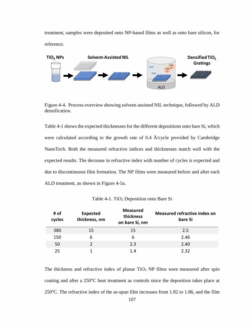
107
treatment, samples were deposited onto NP-based films as well as onto bare silicon, for
reference.
Figure 4-4. Process overview showing solvent-assisted NIL technique, followed by ALD
densification.
Table 4-1 shows the expected thicknesses for the different depositions onto bare Si, which
were calculated according to the growth rate of 0.4 Å/cycle provided by Cambridge
NanoTech. Both the measured refractive indices and thicknesses match well with the
expected results. The decrease in refractive index with number of cycles is expected and
due to discontinuous film formation. The NP films were measured before and after each
ALD treatment, as shown in Figure 4-5a.
Table 4-1. TiO2 Deposition onto Bare Si
# of cycles
Expected thickness, nm
Measured thickness
on bare Si, nm
Measured refractive index on bare Si
380 15 15 2.5
150 6 6 2.46
50 2 2.3 2.40
25 1 1.4 2.32
The thickness and refractive index of planar TiO2 NP films were measured after spin
coating and after a 250oC heat treatment as controls since the deposition takes place at
250oC. The refractive index of the as-spun film increases from 1.82 to 1.86, and the film
ALD
TDMATTDM
AT
TiO2 NPs Solvent-Assisted NIL Densified TiO2
GratingsH2O
H2O

108
thickness decreases from 48 to 44 nm after a 2-hour 250oC heat treatment. These slight
changes can be attributed to a mild densification of the NP film. To determine the effect
of ALD onto TiO2 NP films, we prepared several thin films from our NP dispersions and
subjected them to various numbers of ALD cycles, as summarized in Figure 4-5.
Figure 4-5. a) Refractive indices (nD) and thicknesses of TiO2 NP films after 25, 50, 150,
and 380 ALD cycles, b) refractive indices vs wavelength of TiO2 NP films before ALD
(green), after ALD (blue) of TiO2 ALD onto bare silicon, and SEM images of c) NP film
with no ALD, d) 50 cycles of ALD, and e) 150 cycles of ALD.
From Figure 4-5a, after 380 ALD cycles the measured total film thickness is 72 nm and
the refractive index is 2.26, however after just 25 cycles, there is a negligible change in
film thickness accompanied by an approximately 24% increase in refractive index. The
full refractive index as a function of wavelength for 50 cycles of ALD (Figure 4-5b)
emphasizes the dramatic, near-bulk values that can achieved by ALD. The results imply
that the intrinsic porosity of the NP films is being decreased by ALD, which can also be
observed from the change in film surface morphology in Figure 4-5c, d, and e, with
0 cycles 50 cycles 150 cycles
# ALD cycles Refractive Index, nD Thickness, nm
25 2.25 44
50 2.27 46
150 2.26 54
380 2.26 72
a.
1.6
1.8
2
2.2
2.4
2.6
450 550 650 750 850 950 1050 1150
Ref
ract
ive
Inde
x
Wavelength, nm
TiO2 ALD on Si
TiO2 NP + ALD
TiO2 NP as-spun50 cycles
b.
TiO2 NP 250oC
c. d. e.

109
increasing ALD cycles. Using the Lorentz-Lorenz equation (below), we calculated the
porosity of the NP films after spin after 0, 25, 50, 150, and 380 ALD cycles before and
after a 4-hour 475oC heat treatment, as shown in Table 4-2.
𝑓2 =(𝐶 − 𝐴)
(𝐵 − 𝐴), 𝑣𝑜𝑙𝑢𝑚𝑒 𝑓𝑟𝑎𝑐𝑡𝑖𝑜𝑛 𝑐𝑜𝑚𝑝𝑜𝑛𝑒𝑛𝑡 2
𝐴 =(𝑛1
2−1)
(𝑛12+2)
, 𝐵 =(𝑛2
2−1)
(𝑛22+2)
, 𝐶 =(𝑛2−1)
(𝑛2+2)
Here, f2 is the volume fraction of air, n is the measured refractive index (Figure 4-6) and
n1 and n2 are the refractive indices of bulk TiO2 and air, respectively. using the measured
refractive indices.
Table 4-2. Porosity Calculated from Lorentz-Lorenz Equation
# ALD cycles Porosity, %
Before heating After heating
0 31.1 28.1
25 9.0 6.9
50 8.1 6.5
150 8.5 6.9
380 8.5 6.9
The NP films with no ALD treatment resulted in about 30% porosity, which is the cause
for the relatively low refractive index value of 1.82 (compared to nD = 2.488 of bulk
TiO2). After heating, the untreated sample decreases in porosity, but remains close to
30%. However, after 50 ALD cycles onto the NP films, we observe a dramatic decrease
in the porosity by over 20%, corresponding to an increased refractive index (Figure 4-
6a).

110
Figure 4-6. a) film refractive index before (black) and after (red) ALD treatment for
various numbers of cycles, and b) calculated shrinkage of films after heating at 475oC for
4 hrs.
Additionally, after heating this sample, the porosity decreases by just 1.6%, compared to
3% for the untreated sample. These results suggest that 25 to 50 cycles of ALD is an
effective method to decrease film porosity, which leads to enhanced refractive index
values for our films. The decrease in void volume, or porosity, leads favorably to a
decrease in shrinkage upon heating, as demonstrated in Figure 4-6b. Additionally, the
surface roughness (rms) of the NP films before ALD was 2.1±0.1 nm and did not change
significantly after ALD, which is an important consideration for optical applications as
undesired scattering will be detrimental to performance. Figure 4-7 shows AFM scans of
the surface of TiO2 nanoparticle films were collected before and after ALD. The surface
roughness of the film before ALD was 2.2 nm, 2.5 nm after 25 cycles, and 1.9 nm after
50 cycles, suggesting that there is no appreciable change in the roughness due to ALD of
TiO2 into the TiO2 nanoparticle films.
0
5
10
15
20
0 100 200 300 400
Shri
nka
ge, %
# ALD cycles
ALD on TiO2 NP
ALD on Si
a. b.
1.8
2.0
2.2
2.4
2.6
0 100 200 300 400
Ref
ract
ive
inde
x (5
89 n
m)
# ALD cycles
ALD on TiO2 NP, beforeALD on TiO2 NP, afterALD on Si, beforeALD on Si, after

111
Figure 4-7. AFM images of TiO2 nanoparticle films before and after ALD.
4.3.3 ALD onto Patterned Surfaces
Unlike planar films, from which the refractive index can be reliably measured,
confirming the deposition by ALD into the pores of patterned surfaces requires different
techniques. To confirm the deposition into the pores using ALD, aluminum oxide (Al2O3)
was deposited onto TiO2 gratings and EDS was used to observe the presence of oxygen,
aluminum, and titanium throughout the grating, as shown in Figure 4-8. In this
experiment, Al2O3 was deposited over 100 ALD cycles into the imprinted lines in order
to achieve elemental contrast between the imprinted particles and ALD deposited
material.
Figure 4-8. Tilted cross section and closeup (inset) of imprinted TiO2 NP-based gratings
before (a) and after (b) 100 cycles of Al2O3 deposition, and EDS images of a grating cross
section (c) showing aluminum (d), oxygen (e), and titanium (f).
No ALD 25 cycles 50 cycles
Al TiOCross Section EDS
1 um 1 um
250 nm 250 nm
ALDNo ALDa b
c ed f

112
From the tilted cross section images (Figure 4-8a, b), there is no noticeable change in
feature size or surface texture by ALD. EDS from this cross section (Figure 4-8c-f)
indicates that oxygen is present throughout the grating, which is as expected, since
oxygen is a component of both TiO2 and Al2O3. The presence of aluminum in Figure 4-
8d suggests a gradient filling; aluminum is more concentrated on the edges of the grating
with diminishing concentration in the grating’s interior. The opposite is shown for
titanium, with the results indicating titanium is concentrated in the grating’s interior
(Figure 4-8f). These findings are in agreement with the expected results: Al2O3 first
deposits inside the nanoparticle pores, then continues to deposit conformally on the
outside of the grating. With this confirmation, we proceed to densify patterned TiO2 NP-
based structures with TiO2 from ALD.
However, to be useful for photonic and metasurface applications, patterned
structures with ARs greater than 1 are necessary. Therefore, we also demonstrate the
imprinting of TiO2 structures with increased ARs. To the authors’ knowledge this is the
first demonstration of NP-based pillars produced by soft lithography with such high ARs,
which creates new opportunities for cost-effective fabrication of optical materials. The
pillars imprinted in Figure 4-9 and 4-10 are produced by our direct patterning technique,
requiring no etching or resist-removal steps and can be scaled to wafer-based production.
Unlike in the case of the modest line gratings, the HAR pillars require a through-stamp
annealing treatment before stamp removal to encourage enough binding between the NPs
to ensure the pillars do not break during stamp removal. After placing the PDMS stamp
onto the NP film, the solvent was allowed to dry out on a hotplate and then the substrate-
stamp assembly was subjected to 20s of NIR irradiation.

113
Figure 4-9. Large area top (a) and tilted cross-sectional view (b) of imprinted TiO2 NP
pillars. Top and cross-sectional views of polymer imprint (c, e) and, top and cross-
sectional view of TiO2 NP imprint (d, f).
The pillars can be effectively patterned over large areas as shown in Figure 4-9a and b,
limited here by the Si master patterned area. In order to compare the change in feature
dimension from the master and the NP imprints, a UV-curable polymer, NOA60, was
imprinted, as shown in Figure 4-9c and e. For the HAR pillar section corresponding to
“section E” on the silicon master, the diameter of the imprinted NOA60 pillars is
measured to be 140±5 nm at the top of the pillar and the height to be 1.1 µm, resulting in
an AR of 7.9. However, the imprinted TiO2 (Figure 4-9d and f) from the same section
50 um
a
10 um
b
1 um
1 um
c
1 um
1 um
d
1 um
e f

114
measures 130±4 nm in diameter and 815 nm in height, resulting in an AR of 6.3.
Compared to the NOA imprints, the measured shrinkage of the NP pillars with respect to
the master is less than 10% in diameter, however, in height the shrinkage is 26%. The
shrinkage results from the solvent-assisted imprinting technique; the solvent-dispersed
NPs fill the PDMS stamp by capillary forces and then the solvent diffuses through the
stamp, resulting in a underfilled mold volume. To achieve specific imprinted feature
dimensions the master mold could be fabricated to include the compensation for
shrinkage.
Figure 4-10a and c show HAR TiO2 pillars as-imprinted and Figure 4-10b and d
show the same pillar area after 50 cycles of TiO2 ALD. No obvious change in the
structures is observed, indicating that the deposited TiO2 is not simply deposited on the
surface, as predicted by the results in Figures 4-5 and 4-8. One observed change between
the HAR pillars before and after ALD is the slight increase in AR after ALD, which most
likely arises from mild shrinkage from heating during ALD (250oC). The height and
diameter of the TiO2 imprinted HAR pillars from “section G” of the silicon master were
measured based on SEM images and are displayed in Table 4-3. After ALD, the diameter
decreases from 170 to 160 nm, which can be attributed to the mild shrinkage that occurs
during the heated ALD step (250oC). However, a small increase in height is also observed,
which is mostly likely due to local variations in height of the imprinted sample.
Table 4-3. Changes in Feature Dimension Before and After ALD
Section Height, nm Diameter, nm (top)
G 830+-7 170 +-7
G - ALD 833 +-9 161 +-4
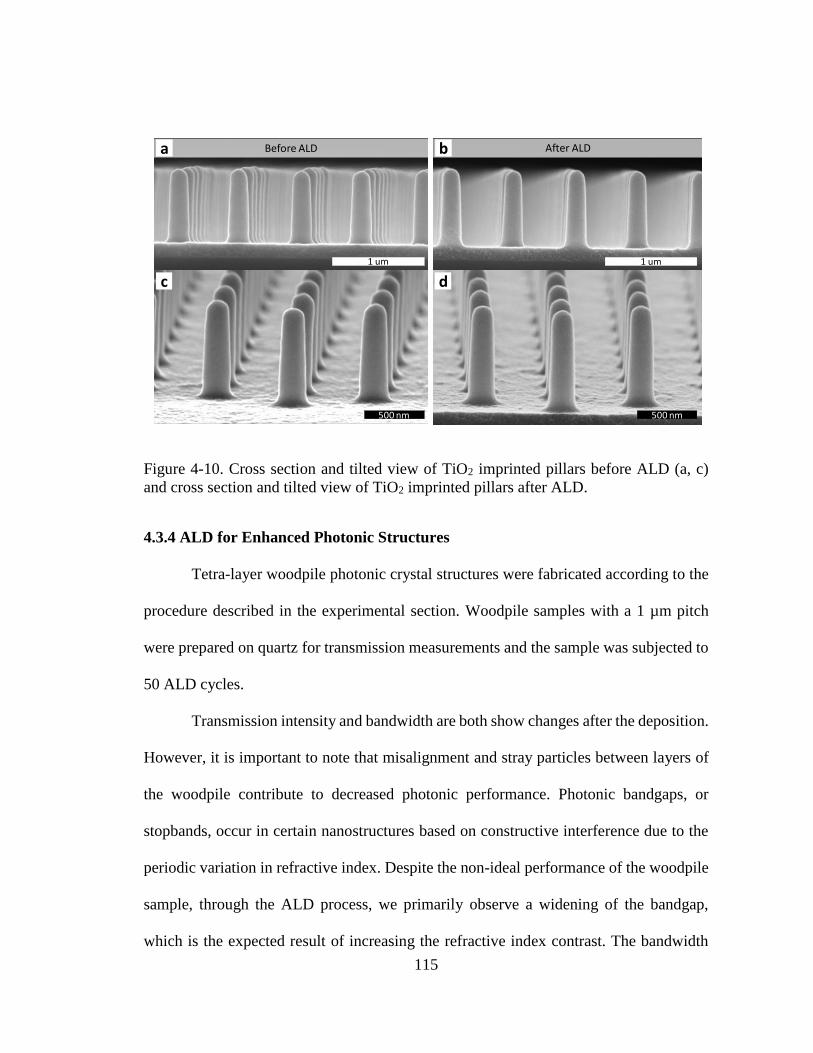
115
Figure 4-10. Cross section and tilted view of TiO2 imprinted pillars before ALD (a, c)
and cross section and tilted view of TiO2 imprinted pillars after ALD.
4.3.4 ALD for Enhanced Photonic Structures
Tetra-layer woodpile photonic crystal structures were fabricated according to the
procedure described in the experimental section. Woodpile samples with a 1 µm pitch
were prepared on quartz for transmission measurements and the sample was subjected to
50 ALD cycles.
Transmission intensity and bandwidth are both show changes after the deposition.
However, it is important to note that misalignment and stray particles between layers of
the woodpile contribute to decreased photonic performance. Photonic bandgaps, or
stopbands, occur in certain nanostructures based on constructive interference due to the
periodic variation in refractive index. Despite the non-ideal performance of the woodpile
sample, through the ALD process, we primarily observe a widening of the bandgap,
which is the expected result of increasing the refractive index contrast. The bandwidth
500 nm500 nm
1 um
After ALDb
1 um
Before ALDa
dc

116
depends on refractive index contrast, while stopband intensity depends on both refractive
index contrast and number of periods30,31.
Figure 4-11. Experimental transmission and reflection intensity of 4-layer woodpile
structures before and after ALD.
4.3.5 Tunability of All-Inorganic TiO2 Films
While achieving the highest refractive index possible is desired in many
applications, the ability to tune the refractive index over a range of values opens the door
to situations requiring precise index tailoring, matching, and/or grading. The films in
Figure 4-12 were prepared by spin coating TiO2 NP films for five seconds, and then
further dried on a hotplate at 60oC for two minutes, which mimics the conditions used to
generate nanopatterns through solvent-assisted NIL. It should be noted that this results in
a slightly lower starting refractive index value (0 cycles ALD), compared to the films in
Figure 4-5a. This can be attributed to differences in NP packing; films spin-coated until
complete solvent removal pack more densely32 and have a slightly higher value (1.82
versus 1.77). The refractive index (nD) increases linearly with the number of ALD cycles
0
0.2
0.4
0.6
0.8
1
200 400 600 800 1000 1200 1400 1600 1800
Tran
smis
sio
n In
ten
sity
Wavelength (nm)
Before ALD
After ALD

117
between 2 and 15, as shown in Figure 4-12a, which allows access to intermediate index
values, which can be used to fabricate gradient refractive index (GRIN) lenses. This
method of tunability benefits from being completely inorganic and composed of a single
material. All-inorganic materials are desirable in many applications where durability and
UV-stability are concerns. Additionally, by using only TiO2, compatibility between the
two materials is ensured. A demonstration of the refractive index tunability was fabricated
by using a simple PDMS mask. Different portions of the NP film were covered during
deposition cycles, resulting in a refractive index gradient/contrast across the surface, as
shown in Figure 4-12b-c. Comparing Figure 4-12c and d, we can see that the deposition
is not resulting in a gradient in thickness, but in a clear gradient in refractive index. The
highest refractive indices correspond to sections that were exposed during the most ALD
cycles, while no such correlation is observed in the thickness map.

118
Figure 4-12. a) Refractive index and calculated porosity of TiO2 NP films subjected to 2,
5, 10, and 15 cycles of ALD, b) spin coated TiO2 film subjected to consecutive rounds of
2 ALD cycles, c) refractive index and d) thickness map of gradient sample, and e)
refractive index dispersion along x = 0 of gradient sample.
4.4 Conclusions
We have presented a method for providing high refractive index metal oxide
nanostructures through a method that is fast and scalable. The scalability and
attractiveness of solvent-assisted NIL lies in its enabling of the direct patterning of a wide
a. b.
c. d.
0 cycles
2 cycles
4 cycles
6 cycles
8 cycles
10 cycles
1.7
1.8
1.9
2
2.1
2.2
400 600 800 1000 1200
Ref
ract
ive
Ind
ex
Wavelength, nm
X = 0
Y=-1.6Y=-1.2Y=-0.8Y=-0.4Y=0Y=0.4Y=0.8Y=1.2
0
5
10
15
20
25
30
35
40
1.70
1.75
1.80
1.85
1.90
1.95
2.00
2.05
2.10
2.15
0 5 10 15 20
Po
rosi
ty, %
Ref
ract
ive
Ind
ex (
nD
)
# ALD Cycles
Refractive Index (nD)Porosity (%)
-2 -1 0 1 2-2
-1
0
1
2
Y (c
m)
X (cm)
1.750
1.783
1.817
1.850
1.883
1.917
1.950
1.983
2.017
2.050
Refractive Index
e.
-2 -1 0 1 2-2
-1
0
1
2
Y (c
m)
X (cm)
41.00
41.89
42.78
43.67
44.56
45.44
46.33
47.22
48.11
49.00
Thickness, nm

119
range of multi-dimensional micro- and nanostructures through a controllable method. The
refractive index of NP-based films can be increased quickly through post-processing
ALD cycling. After just 25 cycles, the film porosity decreases by over 20%, and the
refractive index increases from 1.82 to 2.25. We have also shown that HAR TiO2 pillars
can be patterned directly and subsequently densified. Not only is this method of interest
for enhancing optical properties by increasing refractive index, it also provides a versatile
method for fabricating complex nanostructures by designing new stamp patterns as well
as fabricating materials with varied compositions, as we have demonstrated by depositing
Al2O3. The resulting composition can be varied by changing the imprinted NPs as well
as the deposited elements, further increasing versatility and control.
4.5 References
(1) Genevet, P.; Capasso, F.; Aieta, F.; Khorasaninejad, M.; Devlin, R. Recent
Advances in Planar Optics: From Plasmonic to Dielectric Metasurfaces. Optica
2017, 4 (1), 139.
(2) Yu, N.; Genevet, P.; Kats, M. a; Aieta, F.; Tetienne, J.-P.; Capasso, F.; Gaburro,
Z. Light Propagation with Phase Discontinuities Reflection and Refraction.
Science (80-. ). 2011, 334 (6054), 333–337.
(3) Ni, X.; Emani, N. K.; Kildishev, A. V.; Boltasseva, A.; Shalaev, V. M.
Broadband Light Bending with Plasmonic Nanoantennas. Science (80-. ). 2012,
335 (6067), 427.
(4) Niv, A.; Biener, G.; Kleiner, V.; Hasman, E. Propagation-Invariant Vectorial
Bessel Beams Obtained by Use of Quantized Pancharatnam Berry Phase Optical
Elements. Opt. Lett. 2004, 29 (3), 238.
(5) Yin, X.; Ye, Z.; Rho, J.; Wang, Y.; Zhang, X. Photonic Spin Hall Effect at
Metasurfaces. Science (80-. ). 2013, 339 (6126), 1405–1407.
(6) Shitrit, N.; Yulevich, I.; Maguid, E.; Ozeri, D.; Veksler, D.; Kleiner, V.; Hasman,
E. Spin-Optical Metamaterial Route to Spin-Controlled Photonics. Science (80-.
). 2013, 340 (6133), 724–726.

120
(7) Khorasaninejad, M.; Chen, W. T.; Devlin, R. C.; Oh, J.; Zhu, A. Y.; Capasso, F.
Metalenses at Visible Wavelengths: Diffraction-Limited Focusing and
Subwavelength Resolution Imaging. Science (80-. ). 2016, 352 (6290), 1190–
1194.
(8) Devlin, R. C.; Khorasaninejad, M.; Chen, W.-T.; Oh, J.; Capasso, F. Broadband
High-Efficiency Dielectric Metasurfaces for the Visible Spectrum. Proc. Natl.
Acad. Sci. 2016, 113 (38), 10473–10478.
(9) Hultqvist, A.; Edoff, M.; Törndahl, T. Evaluation of Zn-Sn-O Buffer Layers for
CuIn0.5Ga0.5Se2 Solar Cells. Prog. Photovolt Res. Appl. 2011, 19, 478–481.
(10) Kosola, A.; Putkonen, M.; Johansson, L. S.; Niinistö, L. Effect of Annealing in
Processing of Strontium Titanate Thin Films by ALD. Appl. Surf. Sci. 2003, 211
(1–4), 102–112.
(11) Pore, V.; Hatanpää, T.; Ritala, M.; Leskela, M. Atomic Layer Deposition of
Metal Tellurides and Selenides Using Alkylsilyl Compounds of Tellurium and
Selenium. J. Am. Chem. Soc. 2009, 131 (10), 3478–3480.
(12) Johnson, R. W.; Hultqvist, A.; Bent, S. F. A Brief Review of Atomic Layer
Deposition: From Fundamentals to Applications. Mater. Today 2014, 17 (5),
236–246.
(13) Auth, C.; Allen, C.; Blattner, A.; Bergstrom, D.; Brazier, M.; Bost, M.; Buehler,
M.; Chikarmane, V.; Ghani, T.; Glassman, T.; Grover, R.; Han, W.; Hanken, D.;
Hattendorf, M.; Hentges, P.; Heussner, R.; Hicks, J.; Ingerly, D.; Jain, P.;
Jaloviar, S.; James, R.; Jones, D.; Jopling, J.; Joshi, S.; Kenyon, C.; Liu, H.;
McFadden, R.; McIntyre, B.; Neirynck, J.; Parker, C.; Pipes, L.; Post, I.;
Pradhan, S.; Prince, M.; Ramey, S.; Reynolds, T.; Roesler, J.; Sandford, J.;
Seiple, J.; Smith, P.; Thomas, C.; Towner, D.; Troeger, T.; Weber, C.; Yashar,
P.; Zawadzki, K.; Mistry, K. A 22nm High Performance and Low-Power CMOS
Technology Featuring Fully-Depleted Tri-Gate Transistors, Self-Aligned
Contacts and High Density MIM Capacitors. Dig. Tech. Pap. - Symp. VLSI
Technol. 2012, 131–132.
(14) Kapilashrami, M.; Kronawitter, C. X.; Törndahl, T.; Lindahl, J.; Hultqvist, A.;
Wang, W.-C.; Chang, C.-L.; Mao, S. S.; Guo, J. Soft X-Ray Characterization of
Zn1−xSnxOy Electronic Structure for Thin Film Photovoltaics. Phys. Chem.
Chem. Phys. 2012, 14 (29), 10154.
(15) Beckel, D.; Bieberle, H.; Harvey, A.; Infortuna, A.; Muecke, U. P.; Prestat, M.;
Rupp, J. L. M.; Gauckler, L. J. Thin Films for Micro Solid Oxide Fuel Cells. J.
Power Sources 2007, 173 (1), 325–345.

121
(16) Huang, H.; Nakamura, M.; Su, P.; Fasching, R.; Saito, Y.; Prinz, F. B. High-
Performance Ultrathin Solid Oxide Fuel Cells for Low-Temperature Operation.
J. Electrochem. Soc. 2007, 154 (1), B20.
(17) Chou, S. Y.; Krauss, P. R.; Renstrom, P. J. Imprint of Sub-25 Nm Vias and
Trenches in Polymers. Appl. Phys. Lett. 1995, 67 (1995), 3114.
(18) Leitgeb, M.; Nees, D.; Ruttloff, S.; Palfinger, U.; G??tz, J.; Liska, R.; Belegratis,
M. R.; Stadlober, B. Multilength Scale Patterning of Functional Layers by Roll-
to-Roll Ultraviolet-Light-Assisted Nanoimprint Lithography. ACS Nano 2016, 10
(5), 4926–4941.
(19) John, J.; Tang, Y.; Rothstein, J. P.; Watkins, J. J.; Carter, K. R. Large-Area,
Continuous Roll-to-Roll Nanoimprinting with PFPE Composite Molds.
Nanotechnology 2013, 24 (50).
(20) Xia, Y.; Whitesides, G. M. Soft Lithography. Annu. Rev. Mater. Sci. 1998, 28
(12), 153–184.
(21) Verschuuren, M. Substrate Conformal Imprint Lithography for Nanophotonics;
2009.
(22) Lipomi, D.; Martinez, R.; Cademartiri, L.; Whitesides, G. Soft Lithographic
Approaches to Nanofabrication. In Polymer science: a comprehensive reference;
2012; pp 211–231.
(23) Michel, B.; Bernard, A.; Bietsch, A.; Delmarche, E.; Giessler, M.; Juncker, D.;
Kind, H.; Renault, J.-P.; Rothuizen, H.; Schmid, H.; Schmidt-Winkel, P.; Stutz,
R.; Wolf, H. Printing Meets Lithography: Soft Approaches to High-Resolution
Patterning. IBM J. Res. Dev. 2001, 45 (5), 697.
(24) Zou, Y.; Zhang, D.; Lin, H.; Li, L.; Moreel, L.; Zhou, J.; Du, Q.; Ogbuu, O.;
Danto, S.; Musgraves, J. D.; Richardson, K.; Dobson, K. D.; Birkmire, R.; Hu, J.
High-Performance, High-Index-Contrast Chalcogenide Glass Photonics on
Silicon and Unconventional Non-Planar Substrates. Adv. Opt. Mater. 2014, 2 (5),
478–486.
(25) Li, W.; Zhou, Y.; Howell, I. R.; Gai, Y.; Naik, A. R.; Li, S.; Carter, K. R.;
Watkins, J. J. Direct Imprinting of Scalable, High-Performance Woodpile
Electrodes for Three-Dimensional Lithium-Ion Nanobatteries. ACS Appl. Mater.
Interfaces 2018, acsami.7b14649.
(26) Kothari, R.; Beaulieu, M. R.; Hendricks, N. R.; Li, S.; Watkins, J. J. Direct
Patterning of Robust One-Dimensional, Two-Dimensional, and Three-
Dimensional Crystalline Metal Oxide Nanostructures Using Imprint Lithography
and Nanoparticle Dispersion Inks. Chem. Mater. 2017, 29 (9), 3908–3918.

122
(27) Beaulieu, M. R.; Hendricks, N. R.; Watkins, J. J. Large-Area Printing of Optical
Gratings and 3D Photonic Crystals Using Solution-Processable
Nanoparticle/Polymer Composites. ACS Photonics 2014, 1 (9), 799–805.
(28) Li, S.; Kazemi-Moridani, A.; Zhou, Y.; Howell, I. R.; Kothari, R.; Lee, J.-H.;
Watkins, J. J. Wavelength-Selective Three-Dimensional Thermal Emitters via
Imprint Lithography and Conformal Metallization. ACS Appl. Mater. Interfaces
2018, acsami.7b16902.
(29) Howell, I.; Giroire, B.; Garcia, A.; Li, S.; Aymonier, C.; Watkins, J. J.
Fabrication of Plasmonic TiN Nanostructures by Nitridation of Nanoimprinted
TiO 2 Nanoparticles. J. Mater. Chem. C 2018, 1399–1406.
(30) Tarhan, I.; Watson, G. Photonic Band Structure of Fcc Colloidal Crystals. Phys.
Rev. Lett. 1996, 76 (2), 315–318.
(31) Xia, Y. X. Y.; Gates, B.; Park, S. H. P. S. H. Fabrication of Three-Dimensional
Photonic Crystals for Use in the Spectral Region from Ultraviolet to near-
Infrared. J. Light. Technol. 1999, 17 (11), 1956–1962.
(32) Li, C. Refractive Index Engineering and Optical Properties Enhancement by
Polymer Nanocomposites. 2016, No. May 2014.

123
CHAPTER 5
FINAL COMMENTS AND OUTLOOK
This dissertation has discussed fabrication strategies for producing high refractive
index patterned structures. Both, organic/inorganic composite resins and all-inorganic
strategies have been studied and their respective benefits and drawbacks have been
discussed.
The area of nanoimprinting in particular is full of possibilities and many more
interesting studies could be beneficial to the technology. In terms of solvent-assisted soft
NIL, systematic studies on the factors affecting feature replication of complex geometries
and high aspect ratio structures would be critical in advancing scalable production of
metamaterials which are of high-interest. A more in-depth look at how the demolding
forces affect the imprinted nanoparticle-based inks and how to decrease demolding-
introduced defectivity.
Stamp material are another imprinting factor to be considered for improvement.
The current process relies of rubber molds, of which the key features for solvent-assisted
NIL are the conformality and permeability. Conformality allows for flexible imprinting
and localizes any defects. Permeability is key for solvent absorption/removal, which is
critical for nanoparticle patterning. New approaches to stamp materials, such as dynamic
stamps which can change properties after imprinting, could provide a path toward
patterning (demolding) of complex geometries.
124
BIBLIOGRAPHY
(1) Henning, S.; Svensson, L. Production of Silica Aerogel. Phys. Scr. 1981, 23
(4B), 697–702.
(2) Adachi, I.; Sumiyoshi, T.; Hayashi, K.; Iida, N.; Enomoto, R.; Tsukada, K.;
Suda, R.; Matsumoto, S.; Natori, K.; Yokoyama, M.; Yokogawa, H. Study of a
Threshold Cherenkov Counter Based on Silica Aerogels with Low Refractive
Indices. Nucl. Instruments Methods Phys. Res. Sect. A Accel. Spectrometers,
Detect. Assoc. Equip. 1995, 355 (2–3), 390–398.
(3) Higashihara, T.; Ueda, M. Recent Progress in High Refractive Index Polymers.
Macromolecules. 2015, pp 1915–1929.
(4) Liu, J.; Ueda, M. High Refractive Index Polymers: Fundamental Research and
Practical Applications. J. Mater. Chem. 2009, 19 (47), 8907.
(5) Paul, D. R.; Robeson, L. M. Poylmer Nanotechnology: Nanocomposites.
Polymer (Guildf). 2008, 49 (15), 3187–3204.
(6) Balazs, A. C.; Emrick, T.; Russell, T. P. Nanoparticle Polymer Composites:
Where Two Small Worlds Meet. Science (80-. ). 2006, 314 (5802), 1107–1110.
(7) Lan, T.; Pinnavaia, T. J. Clay-Reinforced Epoxy Nanocomposites. Chem. Mater.
1994, 6, 2216–2219.
(8) Wang, M.-J.; Gray, C. A.; Reznek, S. A.; Mahmud, K.; Kutsovsky, Y. Carbon
Black. Kirk-Othmer Encycl. Chem. Technol. 2003.
(9) Sudeep, P. K.; Emrick, T. Polymer-Nanoparticle Composites: Preparative
Methods and Electronically Active Materials. Polym. Rev. 2007, 47 (2), 155–163.
(10) Crosby, A. J.; Lee, J. Y. Polymer Nanocomposites: The “nano” effect on
Mechanical Properties. Polym. Rev. 2007, 47 (2), 217–229.
(11) Gai, Y.; Lin, Y.; Song, D. P.; Yavitt, B. M.; Watkins, J. J. Strong Ligand-Block
Copolymer Interactions for Incorporation of Relatively Large Nanoparticles in
Ordered Composites. Macromolecules 2016, 49 (9), 3352–3360.
(12) Yao, L.; Lin, Y.; Watkins, J. J. Ultrahigh Loading of Nanoparticles into Ordered
Block Copolymer Composites. Macromolecules 2014, 47 (5), 1844–1849.
(13) Aspnes, D. E. Local-Field Effects and Effective-Medium Theory: A Microscopic
Perspective. Am. J. Phys. 1982, 50 (8), 704.
(14) Caseri, W. INORGANIC NANOPARTICLES AS OPTICALLY EFFECTIVE
ADDITIVES FOR POLYMERS. Chem. Eng. Commun. 2009, 196, 549–572.

125
(15) Braun, M. M.; Pilon, L. Effective Optical Properties of Non-Absorbing
Nanoporous Thin Films. Thin Solid Films 2006, 496 (2), 505–514.
(16) Caseri, W. Nanocomposites of Polymers and Metals or Semiconductors:
Historical Background and Optical Properties. Macromol. Rapid Commun. 2000,
21 (11), 705–722.
(17) Krogman, K. C.; Druffel, T.; Sunkara, M. K. Anti-Reflective Optical Coatings
Incorporating Nanoparticles. Nanotechnology 2005, 16, S338–S343.
(18) Nakamura, T.; Fujii, H.; Juni, N.; Tsutsumi, N. Enhanced Coupling of Light from
Organic Electroluminescent Device Using Diffusive Particle Dispersed High
Refractive Index Resin Substrate. Opt. Rev. 2006, 13 (2), 104–110.
(19) Joannopoulos, J. D. Photonic Crystals: Molding the Flow of Light, 2nd Edition;
2008.
(20) Loncar, M.; Doll, T.; Vuckovic, J.; Scherer, A. Design and Fabrication of Silicon
Photonic Crystal Optical Waveguides. J. Light. Technol. 2000, 18 (10), 1402–
1411.
(21) Yablonovitch, E. Photonic Band-Gap Structures. J. Opt. Soc. Am. B 1993, 10 (2),
283.
(22) John, S. Strong Localization of Photons in Certain Disordered Dielectric
Superlattices. Phys. Rev. Lett. 1987, 58 (23), 2486–2489.
(23) Johnson, S. G.; Joannopoulos, J. D. Introduction to Photonic Crystals: Bloch’s
Theorem, Band Diagrams, and Gaps (but No Defects). Photonic Cryst. Tutor.
2003, No. February, 1–16.
(24) Yablonovitch, E. Inhibited Spontaneous Emission in Solid-State Physics and
Electronics. Phys. Rev. Lett. 1987, 58 (20), 2059–2062.
(25) Yu, N.; Capasso, F. Flat Optics with Designer Metasurfaces. Nat. Mater. 2014,
13 (2), 139–150.
(26) Smith, D. R.; Pendry, J. B.; Wiltshire, M. C. K. Metamaterials and Negative
Refractive Index. Science (80-. ). 2004, 305 (5685), 788–792.
(27) Xu, T.; Agrawal, A.; Abashin, M.; Chau, K. J.; Lezec, H. J. All-Angle Negative
Refraction and Active Flat Lensing of Ultraviolet Light. Nature 2013, 497
(7450), 470–474.
(28) Baets, R. Microphotonics - Thin Films. Univ. Gent - Photonic Res. Gr.

126
(29) Caldwell, J. D.; Glembocki, O.; Bezares, F. J.; Bassim, N. D.; Rendell, R. W.;
Feygelson, M.; Ukaegbu, M.; Kasica, R.; Shirey, L.; Hosten, C.; Al, C. E. T.
Plasmonic Nanopillar Arrays for Large Area, High- Enhancement Surface-
Enhanced Raman Scattering Sensors. ACS Nano 2011, 5 (5), 4046–4055.
(30) Stewart, M. Nanostructured Plasmonic Sensors. Chem. Rev. 2008, 108 (2), 494–
521.
(31) Anker, J. N.; Hall, W. P.; Lyandres, O.; Shah, N. C.; Zhao, J.; Van Duyne, R. P.
Biosensing with Plasmonic Nanosensors. Nat. Mater. 2008, 7 (6), 442–453.
(32) Tan, S. J.; Zhang, L.; Zhu, D.; Goh, X. M.; Wang, Y. M.; Kumar, K.; Qiu, C. W.;
Yang, J. K. W. Plasmonic Color Palettes for Photorealistic Printing with
Aluminum Nanostructures. Nano Lett. 2014, 14 (7), 4023–4029.
(33) Naik, G. V.; Shalaev, V. M.; Boltasseva, A. Alternative Plasmonic Materials:
Beyond Gold and Silver. Adv. Mater. 2013, 25 (24), 3264–3294.
(34) Oates, T. W. H.; Wormeester, H.; Arwin, H. Characterization of Plasmonic
Effects in Thin Films and Metamaterials Using Spectroscopic Ellipsometry.
Prog. Surf. Sci. 2011, 86 (11–12), 328–376.
(35) Qu, Y.; Li, Q.; Gong, H.; Du, K.; Bai, S.; Zhao, D.; Ye, H.; Qiu, M. Spatially and
Spectrally Resolved Narrowband Optical Absorber Based on 2D Grating
Nanostructures on Metallic Films. Adv. Opt. Mater. 2016, n/a-n/a.
(36) Atwater, H. A.; Polman, A. Plasmonics for Improved Photovoltaic Devices. Nat.
Mater. 2010, 9 (10), 865–865.
(37) Saha, K.; Agasti, S. S.; Kim, C.; Li, X.; Rotello, V. M. Gold Nanoparticles in
Chemical and Biological Sensing. Chem. Rev. 2012, 112 (5), 2739–2779.
(38) Varghese, L. T.; Fan, L.; Xuan, Y.; Tansarawiput, C.; Kim, S.; Qi, M. Resistless
Nanoimprinting in Metal for Plasmonic Nanostructures. Small 2013, 9 (22),
3778–3783.
(39) Bruning, J. H. Optical Lithography: 40 Years and Holding. 2007, 652004 (March
2007), 652004.
(40) Rai-Choudhury, P. Handbook of Microlithography, Micromchining, and
Microfabrication. 1997.
(41) Pease, R. F. W. Nanolithography and Its Prospects as a Manufacturing
Technology. J. Vac. Sci. Technol. B Microelectron. Nanom. Struct. 1992, 10 (1),
278.
(42) Cerrina, F.; Marrian, C. A Path to Nanolithography. MRS Bull. 1996, 21 (12),
56–62.

127
(43) Manfrinato, V. R.; Zhang, L.; Su, D.; Duan, H.; Hobbs, R. G.; Stach, E. A.;
Berggren, K. K. Resolution Limits of Electron-Beam Lithography toward the
Atomic Scale. Nano Lett. 2013, 13 (4), 1555–1558.
(44) Grigorescu, A. E.; Hagen, C. W. Resists for Sub-20-Nm Electron Beam
Lithography with a Focus on HSQ: State of the Art. Nanotechnology 2009, 20
(29), 292001.
(45) Chou, S. Y.; Krauss, P. R.; Renstrom, P. J. Imprint of Sub-25 Nm Vias and
Trenches in Polymers. Appl. Phys. Lett. 1995, 67 (1995), 3114.
(46) Haisma, J. Mold-Assisted Nanolithography: A Process for Reliable Pattern
Replication. J. Vac. Sci. Technol. B Microelectron. Nanom. Struct. 1996, 14 (6),
4124.
(47) Bender, M.; Fuchs, A.; Plachetka, U.; Kurz, H. Status and Prospects of UV-
Nanoimprint Technology. Microelectron. Eng. 2006, 83 (4–9 SPEC. ISS.), 827–
830.
(48) Xia, Y.; Whitesides, G. M. Soft Lithography. Annu. Rev. Mater. Sci. 1998, 28
(12), 153–184.
(49) Chen, Y.; Roy, E.; Kanamori, Y.; Belotti, M.; Decanini, D. Soft Nanoimprint
Lithography. 2005, 5645, 283–288.
(50) Verschuuren, M. Substrate Conformal Imprint Lithography for Nanophotonics;
2009.
(51) Lan, H. Soft UV Nanoimprint Lithography and Its Applications. Intechopen
2013, 169–195.
(52) Ji, R.; Hornung, M.; Verschuuren, M. A.; van de Laar, R.; van Eekelen, J.;
Plachetka, U.; Moeller, M.; Moormann, C. UV Enhanced Substrate Conformal
Imprint Lithography (UV-SCIL) Technique for Photonic Crystals Patterning in
LED Manufacturing. Microelectron. Eng. 2010, 87 (5–8), 963–967.
(53) Hampton, M. J.; Williams, S. S.; Zhou, Z.; Nunes, J.; Ko, D. H.; Templeton, J.
L.; Samulski, E. T.; DeSimone, J. M. The Patterning of Sub-500 Nm Inorganic
Oxide Structures. Adv. Mater. 2008, 20 (14), 2667–2673.
(54) Beaulieu, M. R.; Hendricks, N. R.; Watkins, J. J. Large-Area Printing of Optical
Gratings and 3D Photonic Crystals Using Solution-Processable
Nanoparticle/Polymer Composites. ACS Photonics 2014, 1 (9), 799–805.
(55) Kothari, R.; Beaulieu, M. R.; Hendricks, N. R.; Li, S.; Watkins, J. J. Direct
Patterning of Robust One-Dimensional, Two-Dimensional, and Three-
Dimensional Crystalline Metal Oxide Nanostructures Using Imprint Lithography
and Nanoparticle Dispersion Inks. Chem. Mater. 2017, 29 (9), 3908–3918.

128
(56) Lee, J. N.; Park, C.; Whitesides, G. M. Solvent Compatibility of
Poly(dimethylsiloxane)-Based Microfluidic Devices. Anal. Chem. 2003, 75 (23),
6544–6554.
(57) Howell, I.; Giroire, B.; Garcia, A.; Li, S.; Aymonier, C.; Watkins, J. J.
Fabrication of Plasmonic TiN Nanostructures by Nitridation of Nanoimprinted
TiO 2 Nanoparticles. J. Mater. Chem. C 2018, 1399–1406.
(58) Li, W.; Zhou, Y.; Howell, I. R.; Gai, Y.; Naik, A. R.; Li, S.; Carter, K. R.;
Watkins, J. J. Direct Imprinting of Scalable, High-Performance Woodpile
Electrodes for Three-Dimensional Lithium-Ion Nanobatteries. ACS Appl. Mater.
Interfaces 2018, acsami.7b14649.
(59) Li, C.; Colella, N. S.; Watkins, J. J. Low-Temperature Fabrication of
Mesoporous Titanium Dioxide Thin Films with Tunable Refractive Indices for
One-Dimensional Photonic Crystals and Sensors on Rigid and Flexible
Substrates. ACS Appl. Mater. Interfaces 2015, 7 (24), 13180–13188.
(60) Brongersma, M. L.; Cui, Y.; Fan, S. Light Management for Photovoltaics Using
High-Index Nanostructures. Nat. Mater. 2014, 13 (5), 451–460.
(61) Wierer, J. J.; David, A.; Megens, M. M. III-Nitride Photonic-Crystal Light-
Emitting Diodes with High Extraction Efficiency. Nat. Photonics 2009, 3 (3),
163–169.
(62) Matsuda, T.; Funae, Y.; Yoshida, M.; Yamamoto, T.; Takaya, T. Optical
Material of High Refractive Index Resin Composed of Sulfur-Containing
Aromatic Methacrylates. J. Appl. Polym. Sci. 2000, 76, 50–54.
(63) Arbabi, A.; Horie, Y.; Bagheri, M.; Faraon, A. Dielectric Metasurfaces for
Complete Control of Phase and Polarization with Subwavelength Spatial
Resolution and High Transmission. Nat. Nanotechnol. 2015, 10 (11), 937–943.
(64) Hunt, N. E. J.; Schubert, E. F.; Logan, R. A.; Zydzik, G. J. Enhanced Spectral
Power Density and Reduced Linewidth at 1.3 Μm in an InGaAsP Quantum Well
Resonant-Cavity Light-Emitting Diode. Appl. Phys. Lett. 1992, 61 (19), 2287–
2289.
(65) Colodrero, S.; Mihi, A.; Haggman, L.; Ocana, M.; Boschloo, G.; Hagfeldt, A.;
Miguez, H. Porous One-Dimensional Photonic Crystals Improve the Power-
Conversion Efficiency of Dye-Sensitized Solar Cells. Adv. Mater. 2009, 21 (7),
764–770.
(66) Calvez, S.; Hastie, J. E.; Guina, M.; Okhotnikov, O. G.; Dawson, M. D.
Semiconductor Disk Lasers for the Generation of Visible and Ultraviolet
Radiation. Laser Photonics Rev. 2009, 3 (5), 407–434.

129
(67) Chiappelli, M. C.; Hayward, R. C. Photonic Multilayer Sensors from Photo-
Crosslinkable Polymer Films. Adv. Mater. 2012, 24 (45), 6100–6104.
(68) Lee, J. H.; Koh, C. Y.; Singer, J. P.; Jeon, S. J.; Maldovan, M.; Stein, O.;
Thomas, E. L. 25th Anniversary Article: Ordered Polymer Structures for the
Engineering of Photons and Phonons. Adv. Mater. 2014, 26 (4), 532–569.
(69) Edrington, A. C.; Urbas, A. M.; Derege, P.; Chen, C. X.; Swager, T. M.;
Hadjichristidis, N.; Xenidou, M.; Fetters, L. J.; Joannopoulos, J. D.; Fink, Y.;
Thomas, E. L. Polymer-Based Photonic Crystals. Adv. Mater. 2001, 13 (6), 421–
425.
(70) Urbas, A.; Sharp, R.; Fink, Y.; Thomas, E. L.; Xenidou, M.; Fetters, L. J.
Tunable Block Copolymer/homopolymer Photonic Crystals. Adv. Mater. 2000,
12 (11), 812–814.
(71) Sveinbjornsson, B. R.; Weitekamp, R. a.; Miyake, G. M.; Xia, Y.; Atwater, H. a.;
Grubbs, R. H. Rapid Self-Assembly of Brush Block Copolymers to Photonic
Crystals. Proc. Natl. Acad. Sci. 2012, 109 (36), 14332–14336.
(72) Calvo, M. E.; Miguez, H. Flexible, Adhesive, and Biocompatible Bragg Mirrors
Based on Polydimethylsiloxane Infiltrated Nanoparticle Multilayers. Chem.
Mater. 2010, 22 (13), 3909–3915.
(73) Kolle, M.; Zheng, B.; Gibbons, N.; Baumberg, J. J.; Steiner, U. Stretch-Tuneable
Dielectric Mirrors and Optical Microcavities. Opt. Express 2010, 18 (5), 4356–
4364.
(74) Chan, E. P.; Walish, J. J.; Urbas, A. M.; Thomas, E. L. Mechanochromic
Photonic Gels. Adv. Mater. 2013, 25 (29), 3934–3947.
(75) Yue, Y.; Kurokawa, T.; Haque, M. A.; Nakajima, T.; Nonoyama, T.; Li, X.;
Kajiwara, I.; Gong, J. P. Mechano-Actuated Ultrafast Full-Colour Switching in
Layered Photonic Hydrogels. Nat. Commun. 2014, 5, 4659.
(76) Ito, K. Slide-Ring Materials Using Topological Supramolecular Architecture.
Curr. Opin. Solid State Mater. Sci. 2010, 14 (2), 28–34.
(77) Noda, Y.; Hayashi, Y.; Ito, K. From Topological Gels to Slide-Ring Materials. J.
Appl. Polym. Sci. 2014, 131 (15), 1–9.
(78) Araki, J.; Ito, K. Recent Advances in the Preparation of Cyclodextrin-Based
Polyrotaxanes and Their Applications to Soft Materials. Soft Matter 2007, 3 (12),
1456.
(79) Chan, E. P.; Walish, J. J.; Thomas, E. L.; Stafford, C. M. Block Copolymer
Photonic Gel for Mechanochromic Sensing. Adv. Mater. 2011, 23 (40), 4702–
4706.

130
(80) Ito, K. Novel Entropic Elasticity of Polymeric Materials: Why Is Slide-Ring Gel
so Soft? Polym. J. 2012, 44 (1), 38–41.
(81) Biró, L. P.; Bálint, Z.; Kertész, K.; Vértesy, Z.; Márk, G. I.; Horváth, Z. E.;
Balázs, J.; Méhn, D.; Kiricsi, I.; Lousse, V.; Vigneron, J. P. Role of Photonic-
Crystal-Type Structures in the Thermal Regulation of a Lycaenid Butterfly Sister
Species Pair. Phys. Rev. E - Stat. Physics, Plasmas, Fluids, Relat. Interdiscip.
Top. 2003, 67 (2), 7.
(82) Sun, J.; Bhushan, B. Structure and Mechanical Properties of Beetle Wings: A
Review. RSC Adv. 2012, 2 (33), 12606.
(83) Zi, J.; Yu, X.; Li, Y.; Hu, X.; Xu, C.; Wang, X.; Liu, X.; Fu, R. Coloration
Strategies in Peacock Feathers. Proc. Natl. Acad. Sci. 2003, 100 (22), 12576–
12578.
(84) Teyssier, J.; Saenko, S. V.; Van Der Marel, D.; Milinkovitch, M. C. Photonic
Crystals Cause Active Colour Change in Chameleons. Nat. Commun. 2015, 6, 1–
7.
(85) Chutinan, A.; Kherani, N. P.; Zukotynski, S. High-Efficiency Photonic Crystal
Solar Cell Architecture. Opt. Express 2009, 17 (11), 8871–8878.
(86) Park, H.-G.; Kim, S.-H.; Kwon, S.-H.; Ju, Y.-G.; Yang, J.-K.; Baek, J.-H.; Kim,
S.-B.; Lee, Y.-H. Electrically Driven Single-Cell Photonic Crystal Laser. Science
(80-. ). 2004, 305 (5689), 1444–1447.
(87) Chow, E.; Grot, a; Mirkarimi, L. W.; Sigalas, M.; Girolami, G. Ultracompact
Biochemical Sensor Built with Two-Dimensional Photonic Crystal Microcavity.
Opt. Lett. 2004, 29 (10), 1093–1095.
(88) Howell, I. R.; Li, C.; Colella, N. S.; Ito, K.; Watkins, J. J. Strain-Tunable One
Dimensional Photonic Crystals Based on Zirconium Dioxide/slide-Ring
Elastomer Nanocomposites for Mechanochromic Sensing. ACS Appl. Mater.
Interfaces 2015, 7 (6), 3641–3646.
(89) Waite, J. H.; Lichtenegger, H. C.; Stucky, G. D.; Hansma, P. Exploring
Molecular and Mechanical Gradients in Structural Bioscaffolds. Biochemistry
2004, 43 (24), 7653–7662.
(90) Claussen, K. U.; Giesa, R.; Scheibel, T.; Schmidt, H. W. Learning from Nature:
Synthesis and Characterization of Longitudinal Polymer Gradient Materials
Inspired by Mussel Byssus Threads. Macromol. Rapid Commun. 2012, 33 (3),
206–211.
(91) Claussen, K. U.; Giesa, R.; Schmidt, H. W. Longitudinal Polymer Gradient
Materials Based on Crosslinked Polymers. Polym. (United Kingdom) 2014, 55
(1), 29–38.

131
(92) Claussen, K. U.; Lintz, E. S.; Giesa, R.; Schmidt, H. W.; Scheibel, T. Protein
Gradient Films of Fibroin and Gelatine. Macromol. Biosci. 2013, 13 (10), 1396–
1403.
(93) Claussen, K. U.; Scheibel, T.; Schmidt, H. W.; Giesa, R. Polymer Gradient
Materials: Can Nature Teach Us New Tricks? Macromol. Mater. Eng. 2012, 297
(10), 938–957.
(94) Claussen, K. U.; Tebbe, M.; Giesa, R.; Schweikart, A.; Fery, A.; Schmidt, H.-W.
Towards Tailored Topography: Facile Preparation of Surface-Wrinkled Gradient
Poly(dimethyl Siloxane) with Continuously Changing Wavelength. RSC Adv.
2012, 2 (27), 10185.
(95) John, J.; Tang, Y.; Rothstein, J. P.; Watkins, J. J.; Carter, K. R. Large-Area,
Continuous Roll-to-Roll Nanoimprinting with PFPE Composite Molds.
Nanotechnology 2013, 24 (50), 505307.
(96) Leitgeb, M.; Nees, D.; Ruttloff, S.; Palfinger, U.; G??tz, J.; Liska, R.; Belegratis,
M. R.; Stadlober, B. Multilength Scale Patterning of Functional Layers by Roll-
to-Roll Ultraviolet-Light-Assisted Nanoimprint Lithography. ACS Nano 2016, 10
(5), 4926–4941.
(97) Thesen, M. W.; Nees, D.; Ruttloff, S.; Rumler, M.; Rommel, M.; Schlachter, F.;
Grützner, S.; Vogler, M.; Schleunitz, A.; Grützner, G. Inkjetable and Photo-
Curable Resists for Large-Area and High-Throughput Roll-to-Roll Nanoimprint
Lithography. J. Micro/Nanolithography, MEMS, MOEMS 2014, 13 (4), 43003.
(98) Chang, C. Y.; Yang, S. Y.; Chu, M. H. Rapid Fabrication of Ultraviolet-Cured
Polymer Microlens Arrays by Soft Roller Stamping Process. Microelectron. Eng.
2007, 84 (2), 355–361.
(99) Brandrup, J.; Immergut, E. H.; Grulke, E. A.; Abe, A.; Bloch, D. R. Polymer
Handbook, 4th Ed.; John Wiley & Sons: New York, 2005.
(100) Kitamura, K.; Okada, K.; Fujita, N.; Nagasaka, Y.; Minoru, U.; Sekimoto, Y.;
Kurata, Y. Fabrication Method of Double-Microlens Array Using Self-Alignment
Technology. Jpn. J. Appl. Phys. 2004, 43 (8B), 5840–5844.
(101) Suwa, M.; Niwa, H.; Tomikawa, M. High Refractive Index Positive Tone Photo-
Sensitive Coating. J. Photopolym. Sci. Technol. 2006, 19 (2), 275–276.
(102) Liu, J.; Nakamura, Y.; Ogura, T.; Shibasaki, Y.; Ando, S.; Ueda, M. Optically
Transparent Sulfur-Containing Polyimide - TiO 2 Nanocomposite Films with
High Refractive Index and Negative Pattern Formation from Poly ( Amic Acid ) -
TiO 2 Nanocomposite Film. 2008, No. 6, 273–281.

132
(103) You, N.; Suzuki, Y.; Yorifuji, D.; Ando, S.; Ueda, M. Synthesis of High
Refractive Index Polyimides Derived from and Aromatic Dianhydrides. 2008,
6361–6366.
(104) Yuwono, A. H.; Liu, B.; Xue, J.; Wang, J.; Elim, H. I.; Ji, W.; Li, Y.; White, T. J.
Controlling the Crystallinity and Nonlinear Optical Properties of Transparent
TiO2 – PMMA Nanohybrids. J. Mater. Chem. 2004, 14, 2978–2987.
(105) Mayer, K. M.; Hafner, J. H. Localized Surface Plasmon Resonance Sensors.
Chem. Rev. 2011, 111 (6), 3828–3857.
(106) Zhang, X.; Liu, Z. Superlenses to Overcome the Diffraction Limit. Nat. Mater.
2008, 7 (6), 435–441.
(107) Fang, N.; Lee, H.; Sun, C.; Zhang, X. Sub-Diffraction-Limited Optical Imaging
with a Silver Superlens. 2005, 1783, 534–538.
(108) Schuller, J. A.; Barnard, E. S.; Cai, W.; Jun, Y. C.; White, J. S.; Brongersma, M.
L. Plasmonics for Extreme Light Concentration and Manipulation. Nat. Mater.
2010, 9 (3), 193–204.
(109) Cai, W.; Chettiar, U.; Kildishev, A.; Shalaev, V. Optical Cloaking with
Metamaterials. Nat. Photonics 2007, 1 (April), 224.
(110) Siozios, A.; Koutsogeorgis, D. C.; Lidorikis, E.; Dimitrakopulos, G. P.;
Kehagias, T.; Zoubos, H.; Komninou, P.; Cranton, W. M.; Kosmidis, C.;
Patsalas, P. Optical Encoding by Plasmon-Based Patterning: Hard and Inorganic
Materials Become Photosensitive. Nano Lett. 2012, 12 (1), 259–263.
(111) Tao, A. R.; Habas, S.; Yang, P. Shape Control of Colloidal Metal Nanocrystals.
Small 2008, 4 (3), 310–325.
(112) Sundaramurthy, A.; Schuck, P. J.; Conley, N. R.; Fromm, D. P.; Kino, G. S.;
Moerner, W. E. Toward Nanometer-Scale Optical Photolithography: Utilizing
the near-Field of Bowtie Optical Nanoantennas. Nano Lett. 2006, 6 (3), 355–360.
(113) Grigorenko, a N.; Geim, a K.; Gleeson, H. F.; Zhang, Y.; Firsov, a a;
Khrushchev, I. Y.; Petrovic, J. Nanofabricated Media with Negative Permeability
at Visible Frequencies. Nature 2005, 438 (7066), 335–338.
(114) Ditlbacher, H.; Krenn, J. R.; Schider, G.; Leitner, A.; Aussenegg, F. R. Two-
Dimensional Optics with Surface Plasmon Polaritons. Appl. Phys. Lett. 2002, 81
(10), 1762–1764.
(115) West, P. R.; Ishii, S.; Naik, G. V.; Emani, N. K.; Shalaev, V. M.; Boltasseva, A.
Searching for Better Plasmonic Materials. Laser Photonics Rev. 2010, 4 (6),
795–808.

133
(116) Guler, U.; Shalaev, V. M.; Boltasseva, A. Nanoparticle Plasmonics: Going
Practical with Transition Metal Nitrides. Mater. Today 2015, 18 (4), 227–237.
(117) Hibbins, A. P.; Sambles, J. R.; Lawrence, C. R. Surface Plasmon-Polariton Study
of the Optical Dielectric Function of Titanium Nitride. J. Mod. Opt. 1998, 45
(10), 2051–2062.
(118) Reinholdt, A.; Pecenka, R.; Pinchuk, A.; Runte, S.; Stepanov, A. L.; Weirich, T.
E.; Kreibig, U. Structural, Compositional, Optical and Colorimetric
Characterization of TiN-Nanoparticles. Eur. Phys. J. D 2004, 31, 69–76.
(119) Cortie, M. B.; Giddings, J.; Dowd, A. Optical Properties and Plasmon
Resonances of Titanium Nitride Nanostructures. Nanotechnology 2010, 21,
115201.
(120) Naik, G. V.; Schroeder, J. L.; Ni, X.; Kildishev, A. V.; Sands, T. D.; Boltasseva,
A. Titanium Nitride as a Plasmonic Material for Visible and near-Infrared
Wavelengths. Appl. Phys. Lett. 2012, 100 (18), 534–537.
(121) Zgrabik, C. M.; Hu, E. L. Optimization of Sputtered Titanium Nitride as a
Tunable Metal for Plasmonic Applications. Opt. Mater. Express 2015, 5 (12),
478–489.
(122) Liu, J.; Guler, U.; Lagutchev, A.; Kildishev, A. V.; Malis, O.; Boltasseva, A.;
Shalaev, V. M. Quasi-Coherent Thermal Emitter Based on Refractory Plasmonic
Materials. Opt. Mater. Express 2015, 5 (12), 1548–1551.
(123) Hamamura, H.; Komiyama, H.; Shimogaki, Y. TiN Films Prepared by Flow
Modulation Chemical Vapor Deposition Using TiCl4 and NH3. Jpn. J. Appl.
Phys. 2001, 40, 1517–1521.
(124) Ritala, M.; Leskelä, M.; Rauhala, E.; Jokinen, J. Atomic Layer Epitaxy Growth
of TiN Thin Films from TiI4 and NH3. J. Electrochem. Soc. 1998, 145, 2914–
2920.
(125) Chowdhury, R.; Vispute, R. D.; Jagannadham, K.; Narayan, J. Characteristics of
Titanium Nitride Films Grown by Pulsed Laser Deposition. J. Mater. Res. 1996,
11, 1458–1469.
(126) Mangamma, G.; Ajikumar, P. K.; Nithya, R.; Sairam, T. N.; Mittal, V. K.;
Kamruddin, M.; Dash, S.; Tyagi, a K. Synthesis and Gas Phase Nitridation of
Nanocrystalline TiO 2. J. Phys. D. Appl. Phys. 2007, 40 (15), 4597.
(127) Romero-Gomez, P.; Rico, V.; Espinos, J. P.; Gonzalez-Elipe, A. R.; Palgrave, R.
G.; Egdell, R. G. Nitridation of Nanocrystalline TiO2 Thin Films by Treatment
with Ammonia. Thin Solid Films 2011, 519 (11), 3587–3595.

134
(128) Jimenez, C.; Langlet, M. Formation of TiN by Nitridation of TiO2 Films
Deposited by Ultrasonically Assisted Sol-Gel Technique. Surf. Coatings Technol.
1994, 68–69, 249–252.
(129) Zukalova, M.; Prochazka, J.; Bastl, Z.; Duchoslav, J.; Rubacek, L.; Havlicek, D.;
Kavan, L. Facile Conversion of Electrospun TiO2 into Titanium
Nitride/oxynitride Fibers. Chem. Mater. 2010, 22 (13), 4045–4055.
(130) Moon, G. D.; Joo, J. B.; Dahl, M.; Jung, H.; Yin, Y. Nitridation and Layered
Assembly of Hollow TiO2 Shells for Electrochemical Energy Storage. Adv.
Funct. Mater. 2014, 24 (6), 848–856.
(131) Kamiya, K.; Nishijima, T.; Tanaka, K. Nitridation of the Sol-Gel-Derived
Titanium Oxide Films by Heating in Ammonia Gas. J. Am. Ceram. Soc. 1990, 73
(9), 2750–2752.
(132) Guler, U.; Zemlyanov, D.; Kim, J.; Wang, Z.; Chandrasekar, R.; Meng, X.;
Stach, E.; Kildishev, A. V; Shalaev, V. M.; Boltasseva, A. Plasmonic Titanium
Nitride Nanostructures via Nitridation of Nanopatterned Titanium Dioxide. 2017.
(133) Michel, B.; Bernard, A.; Bietsch, A.; Delmarche, E.; Giessler, M.; Juncker, D.;
Kind, H.; Renault, J.-P.; Rothuizen, H.; Schmid, H.; Schmidt-Winkel, P.; Stutz,
R.; Wolf, H. Printing Meets Lithography: Soft Approaches to High-Resolution
Patterning. IBM J. Res. Dev. 2001, 45 (5), 697.
(134) Voorkamp, R.; M.A., V.; van Brakel, R. SCIL Nanoimprint Solutions: High-
Volume Soft NIL for Wafer Scale Sub-10nm Resolution. In Proc. SPIE 10032,
32nd European Mask and Lithography Conference; 2016.
(135) Drygaś, M.; Czosnek, C.; Paine, R. T.; Janik, J. F. Two-Stage Aerosol Synthesis
of Titanium Nitride TiN and Titanium Oxynitride TiO xN Y Nanopowders of
Spherical Particle Morphology. Chem. Mater. 2006, 18 (13), 3122–3129.
(136) Genevet, P.; Capasso, F.; Aieta, F.; Khorasaninejad, M.; Devlin, R. Recent
Advances in Planar Optics: From Plasmonic to Dielectric Metasurfaces. Optica
2017, 4 (1), 139.
(137) Yu, N.; Genevet, P.; Kats, M. a; Aieta, F.; Tetienne, J.-P.; Capasso, F.; Gaburro,
Z. Light Propagation with Phase Discontinuities Reflection and Refraction.
Science (80-. ). 2011, 334 (6054), 333–337.
(138) Ni, X.; Emani, N. K.; Kildishev, A. V.; Boltasseva, A.; Shalaev, V. M.
Broadband Light Bending with Plasmonic Nanoantennas. Science (80-. ). 2012,
335 (6067), 427.
(139) Niv, A.; Biener, G.; Kleiner, V.; Hasman, E. Propagation-Invariant Vectorial
Bessel Beams Obtained by Use of Quantized Pancharatnam Berry Phase Optical
Elements. Opt. Lett. 2004, 29 (3), 238.

135
(140) Yin, X.; Ye, Z.; Rho, J.; Wang, Y.; Zhang, X. Photonic Spin Hall Effect at
Metasurfaces. Science (80-. ). 2013, 339 (6126), 1405–1407.
(141) Shitrit, N.; Yulevich, I.; Maguid, E.; Ozeri, D.; Veksler, D.; Kleiner, V.; Hasman,
E. Spin-Optical Metamaterial Route to Spin-Controlled Photonics. Science (80-.
). 2013, 340 (6133), 724–726.
(142) Khorasaninejad, M.; Chen, W. T.; Devlin, R. C.; Oh, J.; Zhu, A. Y.; Capasso, F.
Metalenses at Visible Wavelengths: Diffraction-Limited Focusing and
Subwavelength Resolution Imaging. Science (80-. ). 2016, 352 (6290), 1190–
1194.
(143) Devlin, R. C.; Khorasaninejad, M.; Chen, W.-T.; Oh, J.; Capasso, F. Broadband
High-Efficiency Dielectric Metasurfaces for the Visible Spectrum. Proc. Natl.
Acad. Sci. 2016, 113 (38), 10473–10478.
(144) Hultqvist, A.; Edoff, M.; Törndahl, T. Evaluation of Zn-Sn-O Buffer Layers for
CuIn0.5Ga0.5Se2 Solar Cells. Prog. Photovolt Res. Appl. 2011, 19, 478–481.
(145) Kosola, A.; Putkonen, M.; Johansson, L. S.; Niinistö, L. Effect of Annealing in
Processing of Strontium Titanate Thin Films by ALD. Appl. Surf. Sci. 2003, 211
(1–4), 102–112.
(146) Pore, V.; Hatanpää, T.; Ritala, M.; Leskela, M. Atomic Layer Deposition of
Metal Tellurides and Selenides Using Alkylsilyl Compounds of Tellurium and
Selenium. J. Am. Chem. Soc. 2009, 131 (10), 3478–3480.
(147) Johnson, R. W.; Hultqvist, A.; Bent, S. F. A Brief Review of Atomic Layer
Deposition: From Fundamentals to Applications. Mater. Today 2014, 17 (5),
236–246.
(148) Auth, C.; Allen, C.; Blattner, A.; Bergstrom, D.; Brazier, M.; Bost, M.; Buehler,
M.; Chikarmane, V.; Ghani, T.; Glassman, T.; Grover, R.; Han, W.; Hanken, D.;
Hattendorf, M.; Hentges, P.; Heussner, R.; Hicks, J.; Ingerly, D.; Jain, P.;
Jaloviar, S.; James, R.; Jones, D.; Jopling, J.; Joshi, S.; Kenyon, C.; Liu, H.;
McFadden, R.; McIntyre, B.; Neirynck, J.; Parker, C.; Pipes, L.; Post, I.;
Pradhan, S.; Prince, M.; Ramey, S.; Reynolds, T.; Roesler, J.; Sandford, J.;
Seiple, J.; Smith, P.; Thomas, C.; Towner, D.; Troeger, T.; Weber, C.; Yashar,
P.; Zawadzki, K.; Mistry, K. A 22nm High Performance and Low-Power CMOS
Technology Featuring Fully-Depleted Tri-Gate Transistors, Self-Aligned
Contacts and High Density MIM Capacitors. Dig. Tech. Pap. - Symp. VLSI
Technol. 2012, 131–132.
(149) Kapilashrami, M.; Kronawitter, C. X.; Törndahl, T.; Lindahl, J.; Hultqvist, A.;
Wang, W.-C.; Chang, C.-L.; Mao, S. S.; Guo, J. Soft X-Ray Characterization of
Zn1−xSnxOy Electronic Structure for Thin Film Photovoltaics. Phys. Chem.
Chem. Phys. 2012, 14 (29), 10154.

136
(150) Beckel, D.; Bieberle, H.; Harvey, A.; Infortuna, A.; Muecke, U. P.; Prestat, M.;
Rupp, J. L. M.; Gauckler, L. J. Thin Films for Micro Solid Oxide Fuel Cells. J.
Power Sources 2007, 173 (1), 325–345.
(151) Huang, H.; Nakamura, M.; Su, P.; Fasching, R.; Saito, Y.; Prinz, F. B. High-
Performance Ultrathin Solid Oxide Fuel Cells for Low-Temperature Operation.
J. Electrochem. Soc. 2007, 154 (1), B20.
(152) John, J.; Tang, Y.; Rothstein, J. P.; Watkins, J. J.; Carter, K. R. Large-Area,
Continuous Roll-to-Roll Nanoimprinting with PFPE Composite Molds.
Nanotechnology 2013, 24 (50).
(153) Lipomi, D.; Martinez, R.; Cademartiri, L.; Whitesides, G. Soft Lithographic
Approaches to Nanofabrication. In Polymer science: a comprehensive reference;
2012; pp 211–231.
(154) Zou, Y.; Zhang, D.; Lin, H.; Li, L.; Moreel, L.; Zhou, J.; Du, Q.; Ogbuu, O.;
Danto, S.; Musgraves, J. D.; Richardson, K.; Dobson, K. D.; Birkmire, R.; Hu, J.
High-Performance, High-Index-Contrast Chalcogenide Glass Photonics on
Silicon and Unconventional Non-Planar Substrates. Adv. Opt. Mater. 2014, 2 (5),
478–486.
(155) Li, S.; Kazemi-Moridani, A.; Zhou, Y.; Howell, I. R.; Kothari, R.; Lee, J.-H.;
Watkins, J. J. Wavelength-Selective Three-Dimensional Thermal Emitters via
Imprint Lithography and Conformal Metallization. ACS Appl. Mater. Interfaces
2018, acsami.7b16902.
(156) Tarhan, I.; Watson, G. Photonic Band Structure of Fcc Colloidal Crystals. Phys.
Rev. Lett. 1996, 76 (2), 315–318.
(157) Xia, Y. X. Y.; Gates, B.; Park, S. H. P. S. H. Fabrication of Three-Dimensional
Photonic Crystals for Use in the Spectral Region from Ultraviolet to near-
Infrared. J. Light. Technol. 1999, 17 (11), 1956–1962.
(158) Li, C. Refractive Index Engineering and Optical Properties Enhancement by
Polymer Nanocomposites. 2016, No. May 2014.