faculty of electrical engineering, mathematics & computer...
TRANSCRIPT
University of Twente
Faculty of Electrical Engineering, Mathematics & Computer Science
Frequency Division
Fabian van Houwelingen MSc. Thesis July 2006
Supervisors: prof. dr. ir. B. Nauta
dr. ing. E. Klumperink dr. ir. R. van der Zee
Report number: 67.3168 Chair of Integrated Circuit Design Faculty of Electrical Engineering, Mathematics & Computer Science
University of Twente P. O. Box 217
7500 AE Enschede The Netherlands

0. Table of Contents
1. Preface....................................................................................................................3 2. Introduction............................................................................................................4 3. Frequency divider concept.....................................................................................6 4. Voltage gain and frequency limitations ...............................................................10
4.1 Introduction....................................................................................................10 4.2 Transistor transit frequency ...........................................................................10 4.3 Frequency limit on amplifier stages...............................................................11 4.4 Numerical example ........................................................................................12
5. Implementing the discharge circuit......................................................................14 5.1 Introduction....................................................................................................14 5.2 Implementation suggestions and their limitations .........................................14
6. Delay ....................................................................................................................18 6.1 Introduction....................................................................................................18 6.2 The concept of delay as used for frequency division.....................................18 6.3 Implementation of delay ................................................................................20
7. Superharmonic Injection Locking........................................................................24 7.1 Introduction....................................................................................................24 7.2 Definitions......................................................................................................24 7.3 Loop analysis .................................................................................................25 7.5 First circuit implementation used for simulation ...........................................31 7.6 Enlarging the locking range ...........................................................................37 7.7 Final implementation of frequency divider design ........................................37
8 Phase Noise...........................................................................................................44 8.1 Introduction....................................................................................................44 8.2 Time variant phase noise for a free running ring oscillator ...........................44 8.3 Simulation results...........................................................................................48
9. Divider Performance and Benchmarking.............................................................50 10. Conclusions........................................................................................................52 11. Appendix A........................................................................................................54 13. Appendix C ........................................................................................................62 14. Appendix D........................................................................................................64 15. References..........................................................................................................65

3
1. Preface
This Master Thesis report summarizes the past 8 months of the last year of my study Electrical Engineering at the University of Twente. This master thesis has been an assignment which allowed a great deal of creativity; where on one hand everything should be exactly calculated, simulated, predicted and measured, on the other hand a form of creative and ‘free’ thinking may be necessary in order to find out whether or not it is ‘possible’ to create a certain circuit. This creative process has been a very learnable experience for me. I would like to thank the people who supervised this project; Eric Klumerink and Bram Nauta. I also would like to thank the ICD group to allow me to do a chip-talk presentation about this subject; it yielded some very useful discussions. I also would like to thank Mustafa Acar for discussions regarding the overlap of static and dynamic frequency dividers and Ronan van der Zee, member of the graduation committee. Furthermore I would like to thank my family for all support that has been given throughout the study.

4
2. Introduction In analog RF transceiver circuitry, several components are needed to receive and send signals modulated at a high frequency carrier. A stable frequency ‘generator’ (frequency synthesizer) is a very important building block in a transceiver circuit. This synthesizer should be capable of generating a periodic signal with a very stable and accurate frequency. This periodic signal can be used for instance in clock recovery circuits or mixing stages. When the frequency synthesizer is implemented as a Phase Locked Loop (PLL), the scheme of the synthesizer looks as shown in figure 1. Figure 1 General scheme of PLL circuit. In this circuit, a very stable frequency generated by a crystal (indicated as XTAL) is used to generate a periodic signal. This periodic signal usually has a frequency in the order of 10-300 MHz. A PLL provides a way of multiplying this frequency with a fractional number. The output signal of the PLL is given by the Voltage Controlled
Oscillator (VCO). The blocks “M1 ” and “
N1 ” are frequency dividers (also called
prescalers) which divide the frequency of the incoming signal by an integer value M and N, respectively. The values for M and N define the output frequency off the PLL as
XTALVCOout fNMff *== (1)
For instance, when N = 1 and M = 10, the PLL output frequency is ten times higher than the reference crystal frequency. Because of the feedback loop, which consists of a phase comparator and a loop filter, the VCO is locked in phase to the crystal. This means that the VCO output signal has the frequency stability of the reference signal generated by the crystal. Basically a PLL is an effective way of creating a high frequency periodic signal having a stable and accurate frequency. If the dividers used are programmable (i.e. the divisor number can be altered) the output signal of the PLL can have a programmable frequency. This report focuses on the frequency dividers. As mentioned before, the function of the divider is to divide the frequency of the incoming signal by an integer number. There are several parameters defining the overall performance of the frequency divider. These parameters are given below:
N1
M1
ϕΔ= *KVout
XTAL
VCO
H(ω)

5
1. The power and blind current required from either the VCO or reference crystal driving it. This power is usually defined relative to 1 mW; the unit used for this parameter is dBmW. Because the reference crystal generally has a much lower output frequency than the VCO, the larger blind currents will have to be provided by the VCO. It is important that the required input blind power required does not exceed the capabilities of the VCO.
2. The frequency range at which the divider operates correctly (i.e. divides the frequency by the specified integer number). Different frequency divider topologies have different limits to this frequency range.
3. The maximum input frequency; this is a measure of the maximum speed of the frequency divider
4. The power consumption; i.e. the average current drawn from the power supply.
5. Phase noise at the output of the divider, and the way this phase noise depends on the input signal.
The value of every parameter depends on the type of frequency divider. There are two types of frequency dividers that can be defined:
1. Static Frequency dividers. These types of dividers employ a so called ‘toggle flip-flop’ or T flip-flop. This type of circuit has two states and ‘toggles’ between these states for every incoming low to high transition. This function is equivalent to frequency division by two. Because a T flip flop can keep its state indefinitely during absence of low to high transitions, it operates from all frequencies between DC and a maximum input frequency.
2. Dynamic frequency dividers. This type of dividers differs from the static type in the sense that a dynamic divider cannot maintain one state indefinitely in the absence of an input signal. This restriction implies that there is a minimum frequency as well as a maximum frequency at which the divider operates properly. Dynamic dividers can be divided into two categories; the first category is the so called “Regenerative” or “Miller” frequency divider [1], the second category is the so called “Injection Locked Frequency Divider” [2]. Because both types of dividers have minimum and maximum input frequency at which the divider works properly, the operating range is smaller than the range of a static divider.
In this report, an analogue frequency divider is proposed turns out to work in a fully ‘analog’ way (i.e. it can be described using theory about analog frequency dividers). Therefore, in the main text of the report digital techniques will not be discussed. The concept, on which the proposed frequency divider is based, is given in the following chapter.

6
3. Frequency divider concept The initial goal of this project was to design a frequency divider, working at the highest possible speed that exploits the inherent speed of transistors to almost instantly convert an incoming gate voltage to a drain current. This voltage / current conversion is not limited to the transistor Unity Gain Frequency (or Transit Frequency ft), and therefore maybe the ft limit can be circumvented. The following conceptually drawn circuit exploits this property. Figure 1 Conceptual current source. In this figure, the input of the circuit is the voltage source Vin(t) which is surrounded by 4 transistors. Both PMOS and both NMOS transistors have equal dimensions. NMOS1 and PMOS1 form a CMOS inverter which has its output and input shorted. This way, the inverter is biased such that the drain current of PMOS1 is equal to the drain current of NMOS1. PMOS2 and NMOS2 also form an inverter, which is used as a current source. The output of the circuit is the current Iout(t). If Vin(t) is a binary Return to Zero signal (i.e. Vin(t) is a square wave signal assuming only 2 voltages, one of which is zero volts) the output current Iout(t) also is a binary Return to Zero signal. The phase between Vin(t) and Iout(t) is zero and the output current is equal to
( ) min GtV ⋅ regardless of the frequency of the input signal Vin(t) (Gm is the sum of the average transconductances of PMOS2 and NMOS2). The output of the circuit can be connected to a capacitor, in this case Iout(t) (from now on called I1(t)) is used to charge that capacitor. This is shown in the following figure, the capacitor is called Cint. Figure 2 Current source, a capacitor and a discharge circuit. A second circuit creates a current I2(t) that discharges the same capacitor Cint. For now it is supposed that I2(t) is zero. In this case Vin(t) and VC(t) can be drawn as shown in the following figure.
Iout(t)
- Vin(t) +
PMOS1 PMOS2
NMOS2 NMOS1
Discharge Circuit
I2(t)
I1(t)VC(t)
Cint
7
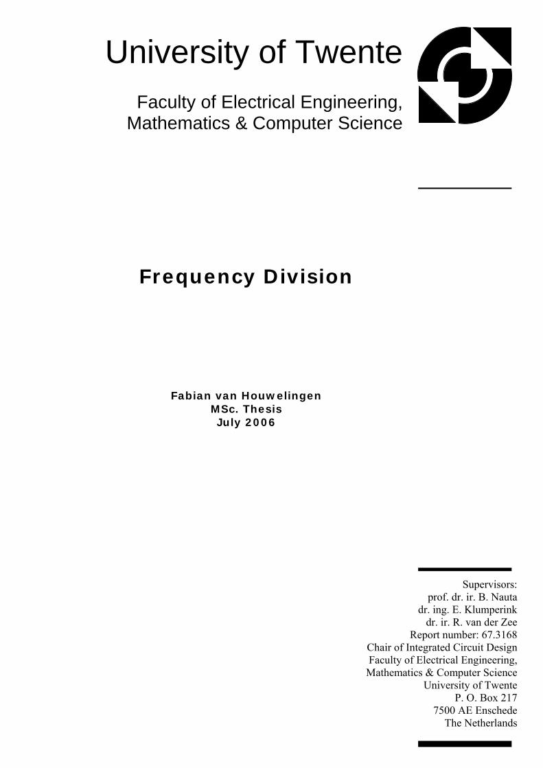
Figure 3 Input voltage and capacitor voltage in case of absence of I2(t). As can be seen in figure 3 the circuit works as a fully linear integrator. If the PMOS2 and NMOS2 devices in figure 2 are modeled as ideal current sources (i.e. their output resistance is infinity and the output current is in phase with the input voltage) this integrator works at arbitrarily high frequencies. This linear integration is a way of creating a timer which ‘counts’ the amount of incoming periods (one period is shown in figure 3 as “Tin”). In order for this circuit to work as a frequency divider, the following additional functions are needed:
• The voltage VC(t) should be compared to a reference voltage, this reference voltage corresponds to an integer amound of periods n·Tin.
• When VC(t) exceeds this voltage, the capacitor should be discharged (this is a way of resetting the timer). For this a current source generating the discharge current I2(t) is needed.
These two functions should be implemented in the “Discharge Circuit” as shown in figure 2. The frequency divider concept is based on the notion that transistors convert voltage into current in an almost infinitely fast way. In order for this concept to be useful, the final implementation of this discharge circuit should not form a speed limitation that is based on the transit frequency ft. Before the implementation of this circuit is considered, the frequency divider concept will be shown by visualizing the signals VC(t), I1(t) and I2(t) in figure 4.
Vin(t)
VC(t)
0 t
0
V
V
t
Tin

8
Figure 4 Charging and discharging a capacitor in order to divide a frequency by 2. This chapter will only consider a frequency division ratio of 2 to keep the analysis simple. For the same reason a square wave input is considered instead of a sine wave (at high frequencies the output of a VCO is more likely to be a sinewave). The discharge circuit has a transfer function VC(t) I2(t). In figure 4 however it is seen that this transfer function is a very unsuitable function, if it has to work at high speeds (see the waveforms in figure 4). This transfer function implies:
• Infinitely fast switching between no current and a relatively large discharge current; conceptually an infinitely small voltage difference in Vc(t) at the input of the discharge circuit should create a current difference of 2I at the output of that circuit. If a voltage controlled current source would be used to discharge
the capacitor Cint, its transconductance should be equal to ∞==ΔΔ
=02I
VIgC
m .
• Strong time variance; once the discharging starts, the current I2(t) should remain high even though the input voltage falls at the same time. It would look as if a ‘memory-capable’ circuit could do this job. However, this ‘memory-capable’ circuit should then be capable of switching off I2 infinitely fast, which causes the same amplification problem.
Maybe the discharge circuit would also work if the transconductance is less than infinity. However that means that the concept itself needs to change. Changes in this concept are made in chapter 5 such that the two ‘impossibilities’ mentioned here can be circumvented and indeed a finite gain suffices. However when making that change, it appears that the discharge circuit implementation will suffer from the ft speed limitation. This process will be described in chapter 5, but first the speed limitation itself is discussed in chapter 4.
I1(t)
VC(t)
0 t
0
V
V
t
Tin
I2(t) 0
t
V
Tout
Vth

9

10
4. Voltage gain and frequency limitations
4.1 Introduction When CMOS implemented circuitry operates at very high frequencies, the ability of the transistors to amplify an incoming signal is limited. A well known property that illustrates this is the “transit frequency”, which is the frequency at which the current gain for a transistor is equal to 1, when its output is shorted. In this paragraph, the transconductance gm of a transistor is assumed a constant.
4.2 Transistor transit frequency Figure 5 Circuit illustrating frequency limitation of transistors. Consider the common source stage depicted in the figure above. The voltage at the gate of the transistor is given by:
( ) ( )tIC
tIC
Vt
G ωω
ω cos1sin100 −== ∫ ∞−
(2)
C is the total impedance seen at the gate (this mainly consists of the gate-source capacitance and the gate-drain capacitance). The gate-source voltage directly relates to the drain current as follows:
( )tIC
ggVI mmGout ω
ωcos* 0−== (3)
When comparing the magnitudes (i.e. absolute values) of the incoming and outgoing currents, the current gain can be derived:
Cg
IIA m
S
out
ω== (4)
The frequency at which this current gain falls to 1 is given by the following equation:
↓Iout
( )tIIS ωsin0=
↑IS
11
Cgf m
t *2π= (6)
This frequency is referred to as the transit frequency. The next paragraph will use this expression for the transit frequency to evaluate the frequency limitation of common source amplifier stages.
4.3 Frequency limit on amplifier stages
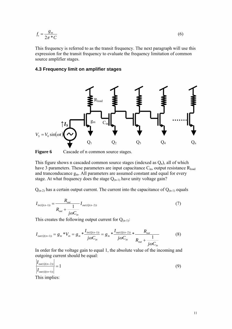
Figure 6 Cascade of n common source stages. This figure shows n cascaded common source stages (indexed as Qn), all of which have 3 parameters. These parameters are input capacitance Cin, output resistance Rload and tranconducance gm. All parameters are assumed constant and equal for every stage. At what frequency does the stage Q(n-1) have unity voltage gain? Q(n-2) has a certain output current. The current into the capacitance of Q(n-1) equals
))2(())1(( 1 −−
+= nQout
inout
outnQin I
CjR
RI
ω
(7)
This creates the following output current for Q(n-1):
inout
out
in
nQoutm
in
nQinminmnQout
CjR
RCj
Ig
CjI
gVgI
ωωω 1**** ))2(())1((
))1((
+=== −−
− (8)
In order for the voltage gain to equal 1, the absolute value of the incoming and outgoing current should be equal:
1))1((
))2(( =−
−
nQout
nQout
I
I (9)
This implies:
( )tVVS ωsin0=
↑IS
Q1 Q2 Q3 Q4 Qn
Rload
gm Cin
12
11* =+
inout
out
in
m
CjR
RCj
g
ωω
(10)
When isolating ω, the unity voltage gain frequency of a common source stage can be found:
outin
outm
RCRg
fπ2
122 −= (11)
When Rout is very high such that gm·Rout >>> 1, then this equation reduces to:
Cgf m
*2π= (12)
This is the transit frequency as previously described. However, the total Rout of a common source stage is bound to a maximum value, due to several reasons. The first reason is the finite output resistance of the NMOS transistor. The following paragraph shows that the actual unity voltage gain frequency for cascaded amplifiers as shown in figure 6 is potentially far lower than the transit frequency of the transistor used.
4.4 Numerical example In this example, equation (11) is evaluated for a single stage NMOS common source amplifier, which amplifies the incoming voltage such that the output voltage swing is large (i.e. is close to both supply rails). This example is important because when a ‘ring oscillator’ is built out of these types of amplifiers, the output voltage swing at each node of this oscillator will be this large. Chapter 5 describes that the actual implementation of the frequency divider is based on an oscillator, and therefore this numerical example will show what actual speed can be expected from a cascade of common source amplifiers. In order to reach maximum speed, the channel length of the transistor will should be the minimum that the CMOS technology allows. In this case a 90 nm process will be considered with a minimum gate length of 0.1 μm. Numerical values for transconductance, output resistance and capacitances are extracted using ProMOST. In the CMOS090 process if a 2/0.1 NMOS is in the strong inversion, saturation region this channel output resistance is in the order 5kΩ − 10kΩ. In order for the NMOS transistor to have a sufficient transconductance, it needs a drain current. A simple model would describe that relation according to:
Doxnm IL
WCg μ2= (13)
In the aforementioned 2/0.1 transistor, this averaged current has an order magnitude of 0.3mA, yielding a transconductance order 1.3 mS. The voltage across the transistor on average is assumed 0.6V. This means that in order for this current to flow into the transistor, the load resistance Rload should have a value in the order of 2 kΩ. This current could also be achieved by using a PMOS current source instead of Rload.

13
This however gives additional problems. If the transistor length is increased, its output resistance obviously increases, however the drain current decreases. This means that the PMOS has to be biased stronger (higher VDS and VGS). Numerical extraction from ProMOST yields a drain current of 0.3mA using a 3/0.15 μm dimensioned transistor (its gate-source voltage set at the maximum supply voltage of 1.2V), which has an output resistance of 3.2 kΩ. However there is a biasing problem; the minimum PMOS drain source voltage needed for this setting is 500 mV, leaving 700 mV of swing for the output voltage of one amplifier stage. This is unacceptable because, as assumed in the beginning of the analysis, the average drain source voltage of the NMOS is 0.6V and its output swing is large. When the drain-source voltage of the PMOST decreases, both its drain current and output resistance decrease. Using a longer transistor channel length than 0.15 μm creates an insufficient drain current which can only be corrected by increasing the channel width (because the VGS bias is already at maximum). However when the width of the channel is increased, the output resistance falls below 2 kΩ. Therefore a PMOS is not a sufficient option if large voltage swings are required. This means that the product gm·Rout now has a magnitude of 2·1.3=2.6. However it gets worse; because very large voltage swings are assumed (close to the supply voltage) there is a certain amount of time at which the input voltage to the NMOS is below the threshold voltage, lowering the average transconductance. When assuming 1.2 V of swing and a threshold voltage of 0.4V, the average transconductance that remains is 0.7 mS. This means that the product gm·Rout now has a magnitude of 2·0.7=1.4. When using these values in (11) (R=2000; gm = 0.0007), the resulting frequency
would beinCe
fπ*34
1= , while the transit frequency is
int Ce
fπ*34.1
1= . This means
that the unity voltage gain of the system is about 0.4·ft, which is a 60 % loss in speed. It can be concluded from this analysis that, for the same gain, a low voltage swing can be amplified at a much higher frequency than a high voltage swing. A single ended free-running ring oscillator creates waveforms which have voltage swings over the entire voltage supply range. This is one of the reasons a ring oscillator generally starts up at a higher frequency than at which it stabilizes [3].

14
↑I2(t) VC (t)
Cgate
I1(t) gm
5. Implementing the discharge circuit
5.1 Introduction In this chapter, the design process of the discharge circuit will be described. As explained in chapter 3, the concept of frequency division using the charge in a capacitor as ‘the time information’ has inherent impossibilities. The goal of this chapter is to show that in order to circumvent these impossibilities an oscillatory circuit can be an effective implementation.
5.2 Implementation suggestions and their limitations Figure 3 shows the total frequency divider. The discharge circuit (shown in figure 2) has an input signal which is the voltage across the capacitor VC(t). Its output signal is the discharge current I2(t). The first design decision made is to keep the value of the capacitor as small as possible, because if there are limitations on the amount of current available to charge and discharge the capacitor, higher voltage swings are possible. The first implementation idea assumes that Cint can be implemented as the capacitance seen at the gate of a transistor. Suppose the discharge circuit is implemented as a single transistor, having a constant transconductance gm and an input gate capacitange Cgate, which is drawn separately from the transistor (see figure 7). Figure 7 Conceptual implementation (left) simplified equivalent circuit (right) Conceptually, this is just a 1-pole linear system that cannot generate any other frequency than that has been put into it. Therefore it cannot be a frequency divider by itself (which has to ‘create’ a new frequency). The transconductance gm shown in figure 6 could be nonlinear however that does not help; it will only create harmonics of the input signal (a frequency divider should create a ‘subharmonic’). An analysis of this circuit is given in Appendix A. This appendix shows that this circuit will work as a low pass filter when a square wave current is assumed to be the input.Suppose the circuit is modified as shown in figure 7.
I2(t)
Cgate
I1(t)
1/gm

15
Figure 8 Modified discharge circuit. It now consists of a separate capacitor Cint (which could be made a lot smaller than a transistor gate capacitance) and a separate transistor, used to discharge the capacitor. The separation element is a switch. The reason to separate the capacitor from the discharge transistor is to create a discharge current that is less dependant on VC(t); the output impedance of the discharge current source has increased from 1/gm to Rout. If the switch is implemented as a transistor, the circuit would look as shown in figure 8 (NMOS1 is the switch): Figure 8 Switch implemented as NMOS (left) and redrawn (right) This circuit is redrawn on the right part of figure 8. Initially VC(t) = 0, NMOS1 is off, Va(t) = 0 and NMOS2 is in deep triode region. When I1(t) charges Cint such that VC(t) is high enough to bring both transistors in saturation region (which is the only way to discharge the capacitor Cint) the small signal impedance seen the when looking into the drain of NMOS1 is equal to Rout2. Although the current source has an increased output impedance (when compared to the previous case depicted in figure 7, where the impedance was 1/gm of the discharge transistor), the total system is still a 1-pole system as described in appendix A and therefore it cannot be a frequency divider. The problem lies in the fact that the transfer between VC(t) and the switch state should be time variant.
↑I2(t) VC (t)
Cint
I1(t) Rout + VDC
↑I2(t)
Cint
I1(t)
Rout1
+ VDC
NMOS1
NMOS2
Va(t)
VC(t)
I1(t)
Cint
Rout2 + VDC
NMOS2
Va(t)
NMOS1
16
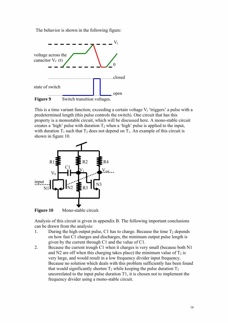
state of switch
voltage across the capacitor VC (t)
open
closed
0
Vt
The behavior is shown in the following figure: Figure 9 Switch transition voltages. This is a time variant function; exceeding a certain voltage Vt ‘triggers’ a pulse with a predetermined length (this pulse controls the switch). One circuit that has this property is a monostable circuit, which will be discussed here. A mono-stable circuit creates a ‘high’ pulse with duration T2 when a ‘high’ pulse is applied to the input, with duration T1 such that T2 does not depend on T1. An example of this circuit is shown in figure 10. Figure 10 Mono-stable circuit. Analysis of this circuit is given in appendix B. The following important conclusions can be drawn from the analysis: 1. During the high output pulse, C1 has to charge. Because the time T2 depends
on how fast C1 charges and discharges, the minimum output pulse length is given by the current through C1 and the value of C1.
2. Because the current trough C1 when it charges is very small (because both N1 and N2 are off when this charging takes place) the minimum value of T2 is very large, and would result in a low frequency divider input frequency. Because no solution which deals with this problem sufficiently has been found that would significantly shorten T2 while keeping the pulse duration T2 uncorrelated to the input pulse duration T1, it is chosen not to implement the frequency divider using a mono-stable circuit.
input
Vout
N1 N2 N3R3
R4R2 R1 C1 V1 V0

17

18
6. Delay
6.1 Introduction This chapter will describe why a delay is the more efficient way to implement the transfer from VC(t) to I2(t). The previous chapter has concluded that in order to implement time variance in the form of a mono-stable circuit, the resulting output frequency will be very limited.
6.2 The concept of delay as used for frequency division Now consider the case where the time variant function in the frequency divider is replaced by a pure delay. In this case, the concept of the charge / discharge model, that was initially defined in figure 4 has to undergo a change: Figure 11 Delay incorporated into the charge / discharge concept. As can be seen in this figure, when the signals -I1(t) and I2(t) are added and integrated with respect to time, the signal shape that results roughly equals the shape of VC(t). As will be shown later, the non-linearities in the implementation of this concept will create a stable state, in which exactly 1 period of I2(t) (which has a length of Tout) contains a charge that is equal to the charge of 2 periods of I1(t) (which has a length of Tin). Because of implementing a delay between the input of the discharge circuit VC(t) and the output I2(t) of the discharge circuit, there is one crucial change: The relation
I1(t)
VC(t)
0 t
0
V
V
t
Tin
I2(t) 0
t
V
Tout

19
input
I2(t)
I1(t)
+ VC(t) -
delay Vd(t)
Cint
between the input voltage VC(t) and the output current I2(t) has become less time variant and more linear. This can be seen by evaluating the correlation between both signals in figure 11. I2(t) looks like VC(t) passed through a low pass filter. This creates the possibility of omitting a time variant system like the mono-stable circuit shown in figure 10. The components needed when implementing a frequency divider based on a form of delay can be summarized as follows:
1. The Integration Capacitor Cint. 2. A current source which charges the capacitor. 3. A current source discharging the capacitor. 4. A form of delay. 5. A form of non-linearity that creates a stable condition; without this delay it is
impossible to exactly match the current of both current sources. This non-linearity will be discussed in chapter 6.
The following figure will show the general scheme of such a frequency divider. Figure 13 Frequency divider based on delay function In this scheme, from now on the ‘charge’ transistor (the green block in figure 10) is a PMOS and the ‘discharge’ transistor (the orange block) is an NMOS. Both are used as common source stages. The next paragraph discusses possible implementations of this scheme.

20
6.3 Implementation of delay The delay concept as used in the general scheme has been put in a conceptual circuit shown below. Figure 14 Delay implemented in frequency divider topology. Figure 14 shows that the delay block is in between the capacitor and the discharge transistor. This paragraph supposes that in order for Cint to be as small as possible (this is needed to ensure the highest possible speeds as discussed in § 5.2) the delay circuit inherently needs to be an active circuit. If only a passive R-C network would be used, the PMOS1 current source has to charge a significantly larger capacitor than when the delay block is implemented as an amplifier stage. In the latter case, Cint can be a gate capacitance. If a passive solution would be used, the PMOS would have to drive a combination of capacitors and resistors. The following figure gives an example: Figure 15 Delay implemented in a passive way. The resistor / capacitor ladder consists of 2 resistors and 2 capacitors, but this is a fairly random choice. Whatever the implementation of the passive network is, VD(t) inherently has a lower swing than VC(t) because current coming form the PMOS gets wasted into an additional current path. This means that the current gain of NMOS1 needs to increase to make sure that I2 is still sufficiently large. However a larger current gain means inherently a lower frequency, as was discussed in chapter 4.
NMOS1
↑I2(t)
VC (t)
Cint
I1(t)
Delay Vin (t) PMOS1
↑I2(t)
VC (t)
Cint
I1(t)
Vin (t) PMOS1 VD (t)
NMOS1

21
Therefore, the ‘delay block’ shown in figure 14 has to be implemented in an ‘active way rather than a passive way. Figure 16 gives an example of an active implementation.
Figure 16 Delay implemented in an active way. In figure 16 an active solution is presented, which means PMOS1 only has to drive C-int in parallel to the resistance 1/gm of NMOS2. The delay is caused by a single common gate amplifier stage, which has to drive the gate input capacitance of NMOS1. VQ(t) is the voltage at the gate of NMOS1. However as simulations indicate, this circuit assumes a state in which no frequency division takes place. The cause of this is that the linear behavior of this type of circuit dominates at high frequencies. It is very hard to find a full proof that states that for any size of the components shown in figure 16 and any input signal condition the linear behavior will prevail but various simulations show that at high frequencies the output voltage swings of an amplifier stage decrease. Circuit 16 contains 3 amplifier stages. Because all voltage swings decrease at very high frequencies, the transistor transconductances and output resistances will assume a ‘small signal’ value. Therefore a linear analysis is given of the circuit of figure 16. Figure 17 shows a linear model of the circuit. Figure 17 Linear analysis of the circuit shown in figure 16. In this figure, VC,1(t) is the voltage component caused by the current injection from PMOS1:
↑I2(t)
VC (t)
Cint
I1(t)
Vin (t) PMOS1 NMOS1
NMOS2
VQ (t)
R1
VQ (t) VC,2 (t) VC,1(t)
B
A

22
int
1,1, C
VgV inPMOSm
C ω⋅
= (13)
Because the phase shift between Vin (see figure 16) and VC,1) is not relevant, it is omitted in (13). The transfer function A can be written as
( )( ) 1,2,
2,2,
||11||1
NMOSgateNMOSout
NMOSoutNMOSm
CrRjrRg
Aω+
= (14)
The transfer function B can be written as
int1,
1,1,
1 Crjrg
BNMOSout
NMOSoutNMOSm
ω+= (15)
Both A and B are 1 pole low pass transfer functions. The following loop transfer function can be defined:
( )( ) AB
AtVtV
C
Q
+=
1 (16)
Where A and B are defined in (14) and (15). Because A and B are 1-pole functions, the product A·B can not assume the value -1 for any value of ω (that is, the phase shift caused by A·B will never reach π radians). This means that whatever the frequency of I1(t) is, the circuit of figure 16 will behave as a linear filter. The only way to create a ‘new’ frequency (which might be an integer fractional of the input frequency), is to increase the total amount of poles around the loop such that the circuit behaves as a ring oscillator. It is known that if the stages in a ring oscillator suffer from an input capacitance minimum and an output resistance minimum (as was shown in chapter 4), the maximum output frequency of the circuit is only possible with the minimum number of stages. Therefore, it is chosen that the circuit given in figure 16 will be augmented with another amplifier stage within the loop such that a ring oscillator is created. In other words, the ‘delay’ block shown in figure 13 should be implemented as 2 amplifier stages. Because now 2 amplifier stages are used as the ‘delay’, the fastest possible option is to use 2 NMOS common source stages (each common source stage inverts the voltage, when a single stage was implemented like in figure 16, a common source could not be used for this reason). One final design choice is made; instead of charging the capacitor using a PMOS, an NMOS will be used. The advantage of this is that the incoming voltage sinewave needs to provide less input power in order to create the same charge current I1(t), because an NMOS has a larger current gain. It also appears that the locking range of the resulting divider is larger when an NMOS is used for the charging function (the mechanism for this will be explained later on in the report). Summarizing, the frequency divider now has the following aspects: 1. NMOS transistor is charging current source; 2. PMOS transistor is discharging current source; 3. The delay circuit consists of 2 cascaded common source stages. The resulting schematic is shown in figure 15.
23
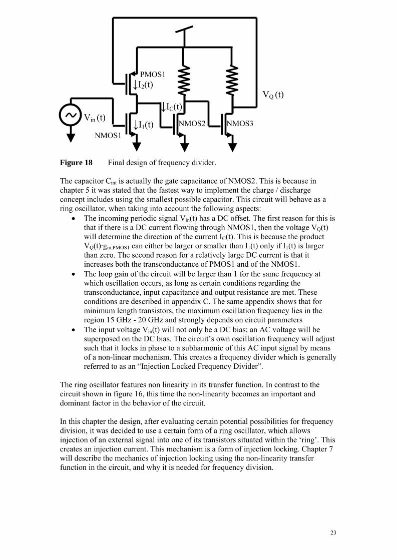
Figure 18 Final design of frequency divider. The capacitor Cint is actually the gate capacitance of NMOS2. This is because in chapter 5 it was stated that the fastest way to implement the charge / discharge concept includes using the smallest possible capacitor. This circuit will behave as a ring oscillator, when taking into account the following aspects:
• The incoming periodic signal Vin(t) has a DC offset. The first reason for this is that if there is a DC current flowing through NMOS1, then the voltage VQ(t) will determine the direction of the current IC(t). This is because the product VQ(t)·gm,PMOS1 can either be larger or smaller than I1(t) only if I1(t) is larger than zero. The second reason for a relatively large DC current is that it increases both the transconductance of PMOS1 and of the NMOS1.
• The loop gain of the circuit will be larger than 1 for the same frequency at which oscillation occurs, as long as certain conditions regarding the transconductance, input capacitance and output resistance are met. These conditions are described in appendix C. The same appendix shows that for minimum length transistors, the maximum oscillation frequency lies in the region 15 GHz - 20 GHz and strongly depends on circuit parameters
• The input voltage Vin(t) will not only be a DC bias; an AC voltage will be superposed on the DC bias. The circuit’s own oscillation frequency will adjust such that it locks in phase to a subharmonic of this AC input signal by means of a non-linear mechanism. This creates a frequency divider which is generally referred to as an “Injection Locked Frequency Divider”.
The ring oscillator features non linearity in its transfer function. In contrast to the circuit shown in figure 16, this time the non-linearity becomes an important and dominant factor in the behavior of the circuit. In this chapter the design, after evaluating certain potential possibilities for frequency division, it was decided to use a certain form of a ring oscillator, which allows injection of an external signal into one of its transistors situated within the ‘ring’. This creates an injection current. This mechanism is a form of injection locking. Chapter 7 will describe the mechanics of injection locking using the non-linearity transfer function in the circuit, and why it is needed for frequency division.
Vin (t) ↓I1(t)
↓I2(t)
NMOS2 NMOS3
NMOS1
PMOS1
VQ (t) ↓IC(t)

24
7. Superharmonic Injection Locking
7.1 Introduction In order for a ring oscillator to work as a frequency divider, its oscillation frequency should track a subharmonic of the injected signal. This can happen if the nonlinearity in the oscillator is such that an intermodulation product of the injected signal and the oscillation already present creates this subharmonic. In order to explain the mechanics of this, a model is made of the circuit shown in figure 16 that incorporates:
• The linear transfer function consisting of a linear gain factor and a lowpass filter;
• The non-linearity that creates amplitude stability and enables the needed intermodulation;
• A node where the incoming current is ‘injected’ into a certain node of the oscillator.
The subsequent analysis presumes a division ratio of 2. This chapter will show that this division ratio provides a ‘locking range’ (i.e. the frequency range over which the injection locked divider works properly) which is large enough to overcome CMOS production process variations, but for this a nontrivial modification has to be made to the circuit initially proposed in figure 18.
7.2 Definitions In order to keep the analysis simple, all present non-linearity is merged into one non-linear transfer function. This creates the model as shown in figure 19. Figure 19 Scheme used to describe the superharmonic injection locking mechanism. In this schematic, the green block represents the voltage controlled current source, which creates the injected current according to
IB(t)
IA(t) ( )( )3322
3232
11)(
CRjCRjGGRRH mm
ωωω
++=
( )( ) ( )∑∞
=
⋅=1
11n
nn tVatVf
inminA GVI _*=
1* moutB GVI −=+
C1 R1
+ V1(t) -
+ Vout(t) -
+ Vin(t) -

25
( ) ( ) inminA GtVtI _⋅= (17) The input voltage Vin is defined as
( ) ( )ϕωξ += tVtV inin cos (18) where Vξ is the amplitude of the incoming voltage and ωin is the angular frequency of the input signal. The orange block is also a voltage controlled current source, which creates the following current:
( ) ( ) 1moutB GtVtI ⋅−= (19) The voltage driving this current source is the actual output voltage of the divider which is defined as
( ) ( )tVtV osout ωψ cos= (20) where Vψ is the amplitude of the output voltage of the ring oscillator and ωos is the angular frequency of the output signal. The output voltage is considered the voltage at node 3 of the ring oscillator (see figure 18). In that figure this voltage is called VQ(t).
7.3 Loop analysis In this paragraph it is calculated how the signals travel though the loop consisting of a non-linear and a linear transfer function. The voltage at node 1 is given by:
( ) ( ) ( )( ) 11 ZtItItV BA ⋅+= (21) Z1 is the impedance seen at node 1 of the ring oscillator and is given by:
11
111 +
=CRj
Zω
(22)
The voltage V1(t) is now subjected to the nonlinearity block which has the following transfer function:
( )( ) ( ) ( ) ( ) ( )∑∞
=
⋅=⋅++⋅+⋅+=1
112
121101 ...n
nn
nn tVatVatVatVaatVf (23)
When substituting for V1, this output can be written as
( )( ) ( ) ( )( )( ) ( ) ( )( )( )n
nmoutinminn
n
nBAn ZGtVGtVaZtItIatVf ∑∑
∞
=
∞
=
⋅⋅−⋅⋅=⋅+⋅=1
11_1
11
It can be proven the output of the nonlinear transfer function can be written as the sum of all possible intermodulation products and harmonics. This proof is given by [4].
( )( ) ( ) ( ) ( )tnVGmtmVGKZtVf osnnn
n min
mmnm
nmminm
ωϕωψξ
cos1cos1_
0 0,11 −⋅+= ∑∑
∞
=
∞
=
+ (25)
Km,n is the 2-dimensional array of coefficients corresponding to these products. The only intermodulation product that will be discussed further on is Vin(t)·Vout(t), which has the coefficient K1,1. There are two reasons for this. The first reason is that this simplifies the calculations; the second reason is that this product is very dominant in the behavior of the circuit. Higher order harmonics are assumed to be filtered out due to the low-pass characteristic of the ring oscillator. Furthermore, the intermodulation coefficients Km,n are considered constant (i.e. non-dependant on the nature of the injected signal or the voltages present inside the loop). Using these simplifications, the product can be written as:

26
( ) ( )
( ) ( )⎟⎠⎞
⎜⎝⎛ +++−+−
=⋅+−
ttttVVGGZK
ttVVGGZK
osinosinminm
osinminm
ωϕωωϕω
ωϕω
ψξ
ψξ
cos21cos
21
coscos
1_2
11,1
1_2
11,1
(26)
During locking at a frequency division ratio of 2, ωinj- ωosc = ωosc holds. The frequency component ωinj+ ωosc will be filtered out as well, which means the total voltage at a frequency of ωosc is equal to the ‘existing’ oscillation voltage added to the intermodulation product K1,1:
( )( ) ( ) ( )ϕωω ψξψ +−−= tVVGGZKtVGZKtVf osminmosm cos21cos 1_
211,1111,01 (27)
This voltage can also be written as ( )( ) ( ) ( )( )ϕωωψ +−−= tTKtKVGZtVf ososm coscos 1,11,0111 (28)
where
2_1 ξVGZ
T inm= (29)
This voltage designated ( )( )tVf 1 passes through the second order linear low-pass filter, which has the following transfer function:
( ) ( )( )3322
3232
11 CRjCRjRRGGH
oscosc
mm
ωωω
++= (30)
The output of this 2-pole transfer function (which actually is the implementation of the “delay” block as described in chapter 6) is the output voltage of the divider Vout:
( ) ( )( ) ( ) ( )( )ϕωωωω ψ ++
++−
= tTKtKVGZCRjCRj
RRGGtV ososmoscosc
mmout coscos
11 1,11,0113322
3232
Z1 is the impedance consisting of R1 parallel C1:
( )11
1
1 CRjR
osω+ (32)
Substituting for Z1 and for Vout(t) gives the following equation:
( ) ( ) ( )( )ϕωωω
ω ψψ ++⋅⎟⎟⎠
⎞⎜⎜⎝
⎛+
−= ∏=
tTKtKVCRj
RGtV ososn nnos
nmnos coscos
1cos 1,11,0
3
1
(33)
This equation provides the operating conditions for superharmonic locking, in case of a frequency division ratio of 2. This equation provides two important boundary conditions; both sides contain a sinusoidal signal with a certain amplitude and phase. Both the magnitude and phase on either side of the equation should match in order to support injection locking. The foregoing assumptions are also applied here, stating that K0,1 and K1,1 are constant (this assumption will be revisited later). In this case, the equation is a completely linear transfer function. This allows replacing the cosine functions with complex exponentials:
( ) ( ) ( ) ( )( )( )ϕωωω
ω ψψ jtjTKtjKVCRj
RGtjV ososn nnos
nmnos expexpexp
1exp 1,11,0
3
1
⋅+⋅⎟⎟⎠
⎞⎜⎜⎝
⎛+
−= ∏=
This equation is generally being referred to as the ‘oscillation condition’ in literature. Dividing both sides by the term ( )tjV osωψ exp gives
( )( ) ( )( ) ( )( )ϕϕϕω sincosexp11,11,11,01,11,0
3
1
TjKTKKjTKKRG
CRjn nmn
nnos ++=+=⎟⎟⎠
⎞⎜⎜⎝
⎛ +−∏
=
7.4 Intuitive analysis on the oscillation condition
27
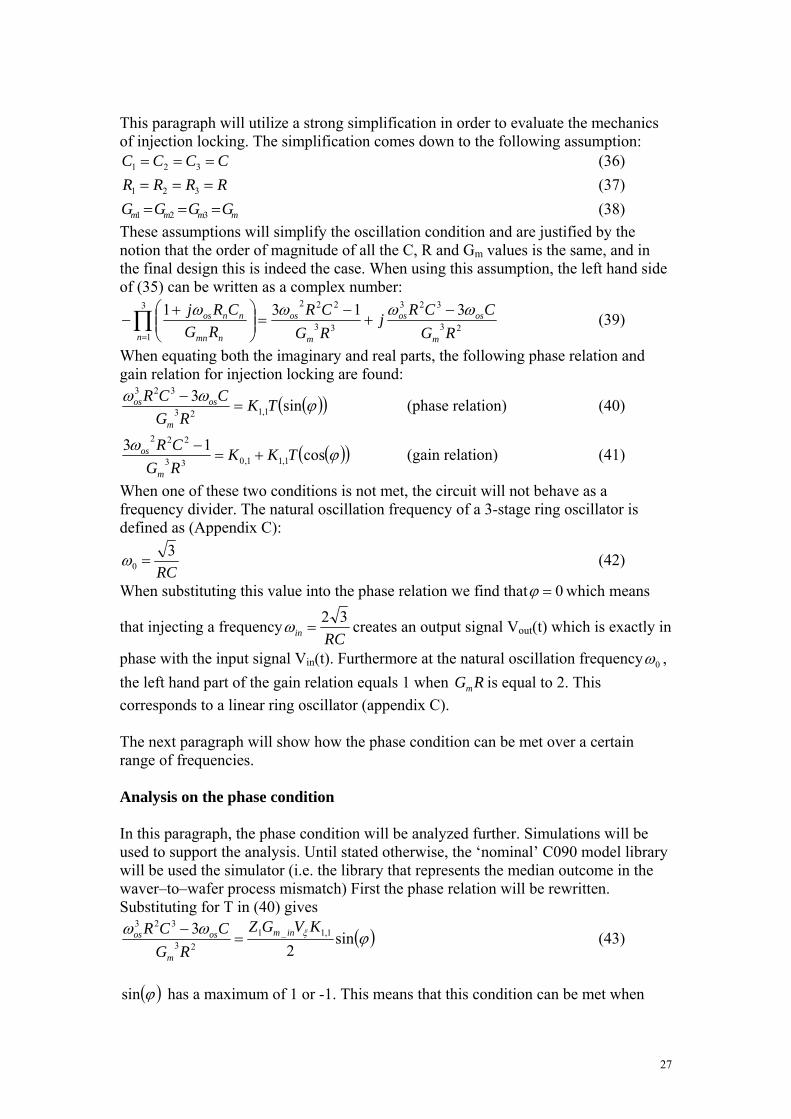
This paragraph will utilize a strong simplification in order to evaluate the mechanics of injection locking. The simplification comes down to the following assumption:
CCCC === 321 (36) RRRR === 321 (37)
mmmm GGGG === 321 (38) These assumptions will simplify the oscillation condition and are justified by the notion that the order of magnitude of all the C, R and Gm values is the same, and in the final design this is indeed the case. When using this assumption, the left hand side of (35) can be written as a complex number:
23
323
33
2223
1
3131RG
CCRjRGCR
RGCRj
m
osos
m
os
n nmn
nnos ωωωω −+
−=⎟⎟
⎠
⎞⎜⎜⎝
⎛ +− ∏
=
(39)
When equating both the imaginary and real parts, the following phase relation and gain relation for injection locking are found:
( )( )ϕωω sin31,123
323
TKRG
CCR
m
osos =− (phase relation) (40)
( )( )ϕω cos131,11,033
222
TKKRGCR
m
os +=− (gain relation) (41)
When one of these two conditions is not met, the circuit will not behave as a frequency divider. The natural oscillation frequency of a 3-stage ring oscillator is defined as (Appendix C):
RC3
0 =ω (42)
When substituting this value into the phase relation we find that 0=ϕ which means
that injecting a frequencyRCin
32=ω creates an output signal Vout(t) which is exactly in
phase with the input signal Vin(t). Furthermore at the natural oscillation frequency 0ω , the left hand part of the gain relation equals 1 when RGm is equal to 2. This corresponds to a linear ring oscillator (appendix C). The next paragraph will show how the phase condition can be met over a certain range of frequencies. Analysis on the phase condition In this paragraph, the phase condition will be analyzed further. Simulations will be used to support the analysis. Until stated otherwise, the ‘nominal’ C090 model library will be used the simulator (i.e. the library that represents the median outcome in the waver–to–wafer process mismatch) First the phase relation will be rewritten. Substituting for T in (40) gives
( )ϕωω ξ sin2
3 1,1_123
323 KVGZRG
CCR inm
m
osos =− (43)
( )ϕsin has a maximum of 1 or -1. This means that this condition can be met when
28
1232
231,1_1
323
≤−
RGKVGZ
CCR
minm
osos
ξ
ωω (44)
That is, when (44) holds, there will be a value of ϕ at which (43) holds. A few important remarks can made about this phase relation:
• When the injection current is increased (by increasing Gm-in or Vξ) the locking range increases (the denominator in the left hand part of (44) increases).
• When the intermodulation product K1,1 increases (i.e. if there is more second order non-linearity) the locking range increases. This can be explained by stating that the circuit actually locks onto a subharmonic of the input frequency. The power of this subharmonic depends on the amount of intermodulation.
• When C or R decreases, the numerator decreases, enhancing the locking range. This can be explained by stating that when the RC-product seen at a node in the oscillator increases, its phase shift increases.
• When Gm increases the locking range also increases. Now the shape of (44) will be provided giving the following assumptions (these assumptions are not accurate, but will provide a qualitative estimate)
• ξV is the input voltage amplitude to the frequency divider, which is 350 mV. • inmG _ is the transconductance of the current source (which is implemented as a
transistor). This transconductance depends biasing conditions (transistor gate, drain and source voltages). Using Appendix C, a transconductance of 0.8 mS is estimated for each stage.
• 1Z is defined by (22) and is a 1-pole low pass transfer function, which transforms the injected current ( )tIB into the voltage ( ) ( )tIZtV BB ⋅= 1 . Only the absolute value of this function 1Z gives the relevant information. When assuming an oscillation frequency ωos = 15 GHz, C = 4 fF and R = 4 kΩ (estimated in appendix C), 1Z is in the order of 3500 Ω.
• The last unknown of the left part of (44) is K1,1. It is given in Appendix D that 21,1 2aK = where a2 is defined in the nonlinear function:
( )( ) ( )∑∞
=
⋅=1
11n
nn tVatVf (45)
Because of the time-variant and voltage swing dependant nature of the nonlinearity, an empirical approach is used to derive a value for a2. In order to derive a2, the nonlinear transfer function block as given in figure 19 is driven by a pure sinewave input. The harmonic distortion at the output of this block is then evaluated, and from the result a2 is extracted.
In this analysis, the non-linear transfer block is assumed to be the combination of MP1, MP2, MN2 and MN18 which are shown in figure 22. When this block is exited with a sine wave having an amplitude of 1.2 V (the swing equals the full supply range) the input and output spectra are as given below:

29
Figure 20 Input and output spectra used to derive a value for a2 This figure shows that a2 has the order of 0.1 (the 30 GHz component is about 10% of the value). This value should however be corrected for the linear lowpass filter and linear amplification that it has already passed through. For 30 GHz this factor is
( ) 117.32.3
115-e43e43e4*4-e8
1==
+⋅⋅=
+=
ωωω
jRCjRGH m (46)
This means a2 still has a value in the order of 0.1. This means K1.1 = 2a2 = 0.2. Now all values needed for (44) can be filled in. This is done using maple, and (44) is plotted with variable ωos , which is varied from 0 to 26 GHz. Figure 21 A plot of the left hand side of (44) with ωos as variable.
input spectrum
output spectrum
ω0
231,1_1
323 62RGKVGZCCR
minm
osos
ξ
ωω −
ωos=21.9 GHz
30
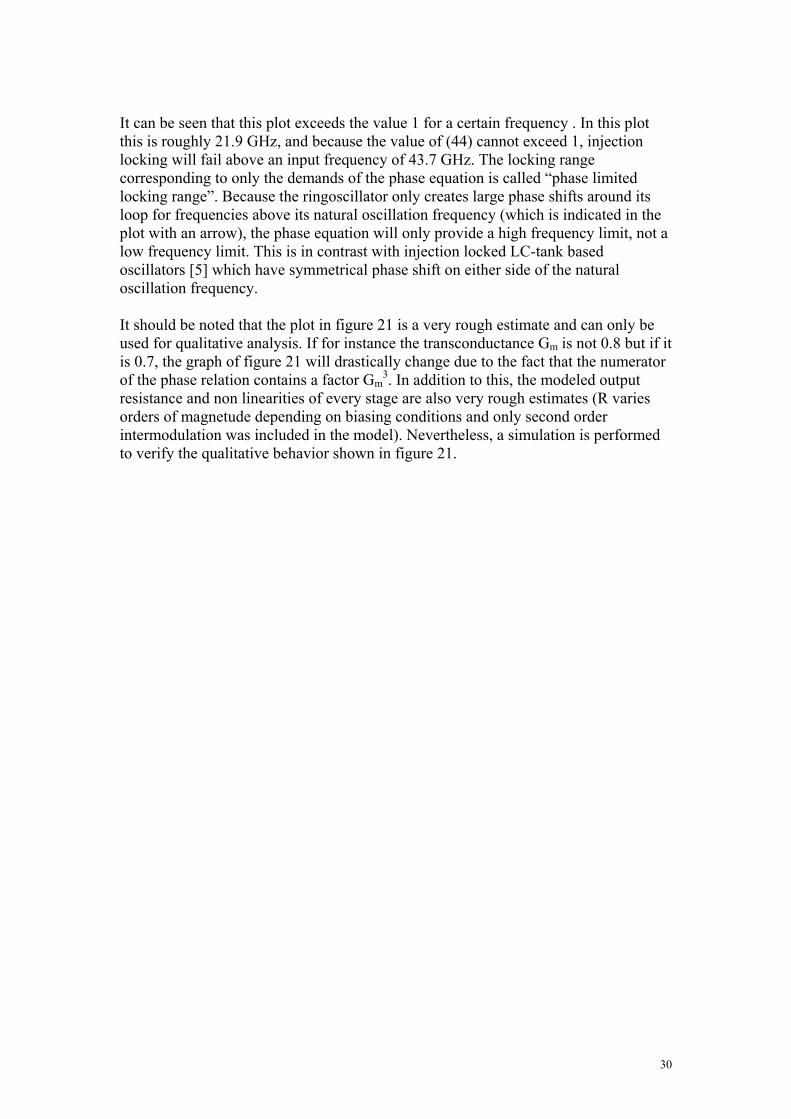
It can be seen that this plot exceeds the value 1 for a certain frequency . In this plot this is roughly 21.9 GHz, and because the value of (44) cannot exceed 1, injection locking will fail above an input frequency of 43.7 GHz. The locking range corresponding to only the demands of the phase equation is called “phase limited locking range”. Because the ringoscillator only creates large phase shifts around its loop for frequencies above its natural oscillation frequency (which is indicated in the plot with an arrow), the phase equation will only provide a high frequency limit, not a low frequency limit. This is in contrast with injection locked LC-tank based oscillators [5] which have symmetrical phase shift on either side of the natural oscillation frequency. It should be noted that the plot in figure 21 is a very rough estimate and can only be used for qualitative analysis. If for instance the transconductance Gm is not 0.8 but if it is 0.7, the graph of figure 21 will drastically change due to the fact that the numerator of the phase relation contains a factor Gm
3. In addition to this, the modeled output resistance and non linearities of every stage are also very rough estimates (R varies orders of magnetude depending on biasing conditions and only second order intermodulation was included in the model). Nevertheless, a simulation is performed to verify the qualitative behavior shown in figure 21.

31
7.5 First circuit implementation used for simulation The first simulation will treat the following implementation of the frequency divider. Figure 22 Version of injection locked frequency divider used for phase analysis. This implementation is different from the one shown in figure 18. The reason this implementation is used, because the circuit is ‘representative’ for the model discussed. A few arguments (based on the analysis discussed in this chapter) suggest that this type of implementation is more suitable to verify outcome of the theoretical analysis. These arguments are described below.
1. When the oscillator runs freely, the voltage swings at the nodes should be large (i.e. close to the supply voltage range). This creates nonlinearity (a ‘clipping sinewave features harmonics). The nonlinearity is needed, because the higher the intermodulation coefficient K1,1, the higher the locking range will be according to (44) Because initially it is assumed a that a PMOS device more effectively pulls a node voltage up to VDD, the resistors in figure 18 are replaced with MP1 and MP2 in figure 22.
2. Furthermore, the resulting voltages at the nodes should not have the form of a squarewave. The reason for this is that a squarewave does not have even harmonics, i.e. the second harmonic coefficient a2 will be theoretically zero. Because a2 is the most important coefficient for division by two, the waveforms at the nodes of the oscillator should not approximate square waves. In order to achieve that it is chosen that NMOS and PMOS transistor sizes are equal (MP1, MP2, MN9 and MN18 of figure 22 are all 2/0.1 μm sized transistors). Because in this way the gm of the NMOS devices will be higher than the gm of the PMOS devices, the voltage waveforms at the nodes will have a higher slew rate downwards than upwards (i.e. the NMOS “pulls” the voltage to GND harder than the PMOS pulls the voltage to VDD). In this way it
32
is made sure that the second order harmonic coefficient a2 is sufficiently present. This was seen in the spectrum plot of figure 20.
3. Because of the strong biasing of MN8 at its gate (VGS = 0.85 V) MP0 has a relatively large W/L ratio (5/0.1) to make sure that MN8 does not pull down the voltage at its drain too much; a second reason for this is to allow MP8 to pass a relatively average high drain current to accommodate a good transconductance for MN8 (this is needed to maximize the ‘injection efficiency’ as defined by T in (29)
4. It is also assumed at this point that very high voltage swings at each oscillator node will make the circuit behavior less dependant on the injected current (i.e. the waveforms at each node are less dictated by the injected signal then by the circuit itself); if a relatively ‘constant’ nonlinearity and transconductance can be assumed these parameters are more predictable (Gm, R and C are predicted in appendix C). This is also achieved by creating large voltage swings.
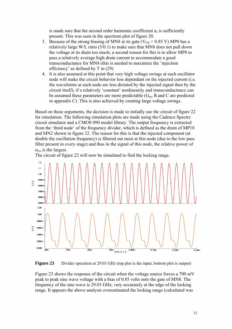
Based on these arguments, the decision is made to initially use the circuit of figure 22 for simulation. The following simulation plots are made using the Cadence Spectre circuit simulator and a CMOS 090 model library. The output frequency is extracted from the ‘third node’ of the frequency divider, which is defined as the drain of MP18 and MN2 shown in figure 22. The reason for this is that the injected component (at double the oscillation frequency) is filtered out most at this node (due to the low pass filter present in every stage) and thus in the signal of this node, the relative power of ωos is the largest. The circuit of figure 22 will now be simulated to find the locking range. Figure 23 Divider operation at 29.03 GHz (top plot is the input, bottom plot is output) Figure 23 shows the response of the circuit when the voltage source forces a 700 mV peak to peak sine wave voltage with a bias of 0.85 volts onto the gate of MN8. The frequency of the sine wave is 29.03 GHz, very accurately at the edge of the locking range. It appears the above analysis overestimated the locking range (calculated was

33
43.7 GHz), but as stated before a minor estimation error in Gm can already make this difference. Important in this plot is that at the highest possible input and output frequency of the circuit shown in figure 22, the voltage swings are still very high (almost the complete supply voltage). When slightly increasing the frequency to 29.05 GHz (which is exceeds the locking range limit by 20 MHz) using the same input amplitude of 700 mV peak to peak, the resulting behavior will be as shown in figure 24. The very low frequency component seen in the bottom plot of that figure (which is the output voltage) is called the ‘Beat Frequency’, and it is a product of a mechanism called “Injection Pulling” [5]. Injection Pulling occurs just outside the phase limited locking range. The figure underneath it (figure 25) shows the operation of the circuit at the bottom edge of the locking range. For this circuit the minimum input frequency for a stable divide-by-two operation is 23.4 GHz. This would create an effective locking range of 5.6 GHz.

34
In order to visualize the low frequency beat frequency, the scale of the horizontal axis of figure 24 is different from the scale used in figure 25. Both plots are simulations on the circuit shown in figure 22. Figure 24 Injection pulling at 29.05 GHz (input is the top plot, output is bottom plot). Figure 25 Divider operation at 23.4 GHz (input is the top plot, output is bottom plot).
35
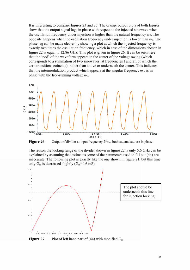
It is interesting to compare figures 23 and 25. The orange output plots of both figures show that the output signal lags in phase with respect to the injected sinewave when the oscillation frequency under injection is higher than the natural frequency ω0. The opposite happens when the oscillation frequency under injection is lower than ω0. The phase lag can be made clearer by showing a plot at which the injected frequency is exactly two times the oscillation frequency, which in case of the dimensions chosen in figure 22 is equal to 12.86 GHz. This plot is given in figure 26. It can be seen here that the ‘nod’ of the waveform appears in the center of the voltage swing (which corresponds to a summation of two sinewaves, at frequencies f and 2f, of which the zero transitions coincide), rather than above or underneath the center. This indicates that the intermodulation product which appears at the angular frequency ωos is in phase with the free-running voltage ω0. Figure 26 Output of divider at input frequency 2*ω0, both ωin and ωos are in phase. The reason the locking range of the divider shown in figure 22 is only 5.6 GHz can be explained by assuming that estimates some of the parameters used to fill out (44) are inaccurate. The following plot is exactly like the one shown in figure 21, but this time only Gm is decreased slightly (Gm=0.6 mS). Figure 27 Plot of left hand part of (44) with modified Gm.
The plot should be underneath this line for injection locking

36
In this plot it can be seen that the phase condition now creates not only a maximum frequency but also a minimum frequency. This could be an explanation for the fact that injection pulling also takes place just below the minimum input frequency (a plot of this is not shown, but looks similar to the plot of figure 24. It can be concluded that this implementation has a very limited locking range (5.6 GHz). The next paragraph describes a way of increasing the locking range of the injection locked frequency divider without having to inject more power (i.e. applying a larger voltage at the input).
37
7.6 Enlarging the locking range In this paragraph an implementation of the frequency divider will be described, that has a larger locking range without using a higher injection voltage (in the entire report, an injection voltage of 700 mV peak to peak is used). It could be seen from the phase relation (44) that the injection power has to increase when the resulting output frequency of the frequency divider deviates more from its natural oscillation frequency. That is, the more distance there is between the natural oscillation frequency and the intermodulation product (which is at the input frequency divided by two) the more injection power is needed to ‘push’ the oscillator to a lower or higher frequency than its natural frequency. In this paragraph a way is proposed to make the “natural oscillation frequency” dependant on the frequency of the injected signal. It is known from chapter 4 that the ‘frequency at unity voltage gain’ of an amplifier stage (when it is placed in a cascade of amplifiers as shown in figure 6) depends on the transistor transconductance, its output resistance and its input capacitance. All three of those parameters depend on the biasing conditions of the transistor. If these biasing conditions (i.e. the DC component of the voltages on each ring oscillator node) can be made dependant of the frequency of the input signal, the natural free running oscillation frequency ω0 of the divider would ‘shift’ to a different value. Conceptually, a form of ‘frequency detection’ has to be implemented to achieve this. An incoming frequency should be ‘converted’ to a certain DC voltage on one or more ring oscillator nodes. There is a way to achieve this goal; consider the case where the voltage swings at the oscillator nodes during free running oscillation are small and at the same time lie close to one of the supply rails. An example in the case of a 1.2 V supply would be a voltage, having a DC component of 900 mV and an AC amplitude of 300 mV (which means the voltage swings between 1.2 V and 0.6 V). Increasing the amplitude of the AC component of that voltage will make the voltage ‘clip’ at the top side against the supply rail of 1.2 V, but it does not clip at the bottom side. This means that the DC component of the voltage has shifted. The key idea is that the injected signal frequency controls the amplitude of those voltage swings. This is because a higher input frequency will be attenuated stronger in the loop, which as a 3rd order low pass filter transfer function. The next paragraph will explain how this idea can be implemented in the frequency divider, which initially looked as shown in figure 22.
7.7 Final implementation of frequency divider design The implementation process starts out with the idea that at least one of the node voltages of the oscillator has to be close to the supply rails. This can be achieved by creating an ‘asymmetrical’ oscillator. Asymmetrical means that at a certain node for instance the NMOS transistor has a higher transconductance than the PMOS transistor. In this case the DC level of the voltage gets pulled to ground stronger than

38
it gets pulled to VDD. However when doing this the problem arises that the next stage will amplify this “low” voltage to a “very high” voltage, which might clip entirely against VDD and therefore kill the AC component of the signal. The actual asymmetry as implemented in the final divider has been chosen such, that the asymmetry itself is maximum while the circuit still oscillates when no injection power is present. The circuit is shown in figure 28. Figure 28 Modified and final version of frequency divider shown in figure 22. In this circuit, the NMOS1 has been made larger than MN8 in figure 22 while keeping the size of PMOS1 equal to the size of MP0 in figure 22. This results in a ‘low’ DC voltage at node 1. This ‘moderately low’ voltage is then amplified by the second stage such that at node 2 a ‘high’ DC voltage emerges. This is also the reason that in figure 22 a PMOS transistor is used; it is capable of pulling up the voltage at node 2 more than a resistor is. The size of the PMOS is relatively slow however. This is due to a speed optimization (when increasing the PMOS size, the overall gm/C ratio of that stage decreases, which decreases the maximum input frequency). The last stage will amplify the ‘high’ voltage at node 2 to a ‘very low’ voltage at node 3. Because this voltage is applied only to PMOS1, and also a high voltage is applied to NMOS1, the voltage at node 1 will be pulled by NMOS1 and PMOS1 at rougly equal rates (which created the ‘moderately low’ DC voltage bias at node 1). Because the job of the 3rd stage is always to pull down the voltage at node 3, a resistor is used in that current path instead of a PMOS (which is a faster implementation). NMOS3 is pretty strongly biased, its gate source voltage is high, and the low value resistor allows a relatively large drain current. This means the transconductance of NMOS3 is high enough to drive the relatively large input capacitance of PMOS1, which forms the load of the 3rd stage. The resulting voltages are shown in the following figure.
Node 3
Node 2
Node 1
39
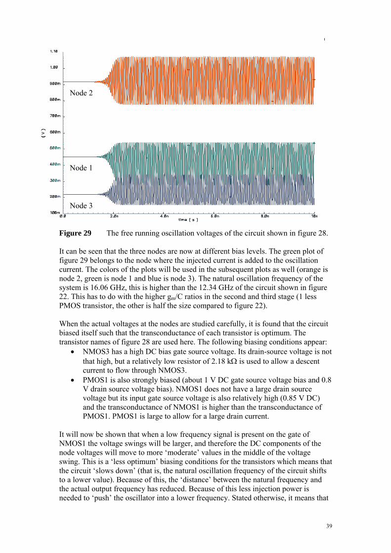
Figure 29 The free running oscillation voltages of the circuit shown in figure 28. It can be seen that the three nodes are now at different bias levels. The green plot of figure 29 belongs to the node where the injected current is added to the oscillation current. The colors of the plots will be used in the subsequent plots as well (orange is node 2, green is node 1 and blue is node 3). The natural oscillation frequency of the system is 16.06 GHz, this is higher than the 12.34 GHz of the circuit shown in figure 22. This has to do with the higher gm/C ratios in the second and third stage (1 less PMOS transistor, the other is half the size compared to figure 22). When the actual voltages at the nodes are studied carefully, it is found that the circuit biased itself such that the transconductance of each transistor is optimum. The transistor names of figure 28 are used here. The following biasing conditions appear:
• NMOS3 has a high DC bias gate source voltage. Its drain-source voltage is not that high, but a relatively low resistor of 2.18 kΩ is used to allow a descent current to flow through NMOS3.
• PMOS1 is also strongly biased (about 1 V DC gate source voltage bias and 0.8 V drain source voltage bias). NMOS1 does not have a large drain source voltage but its input gate source voltage is also relatively high (0.85 V DC) and the transconductance of NMOS1 is higher than the transconductance of PMOS1. PMOS1 is large to allow for a large drain current.
It will now be shown that when a low frequency signal is present on the gate of NMOS1 the voltage swings will be larger, and therefore the DC components of the node voltages will move to more ‘moderate’ values in the middle of the voltage swing. This is a ‘less optimum’ biasing conditions for the transistors which means that the circuit ‘slows down’ (that is, the natural oscillation frequency of the circuit shifts to a lower value). Because of this, the ‘distance’ between the natural frequency and the actual output frequency has reduced. Because of this less injection power is needed to ‘push’ the oscillator into a lower frequency. Stated otherwise, it means that
Node 3
Node 2
Node 1
40
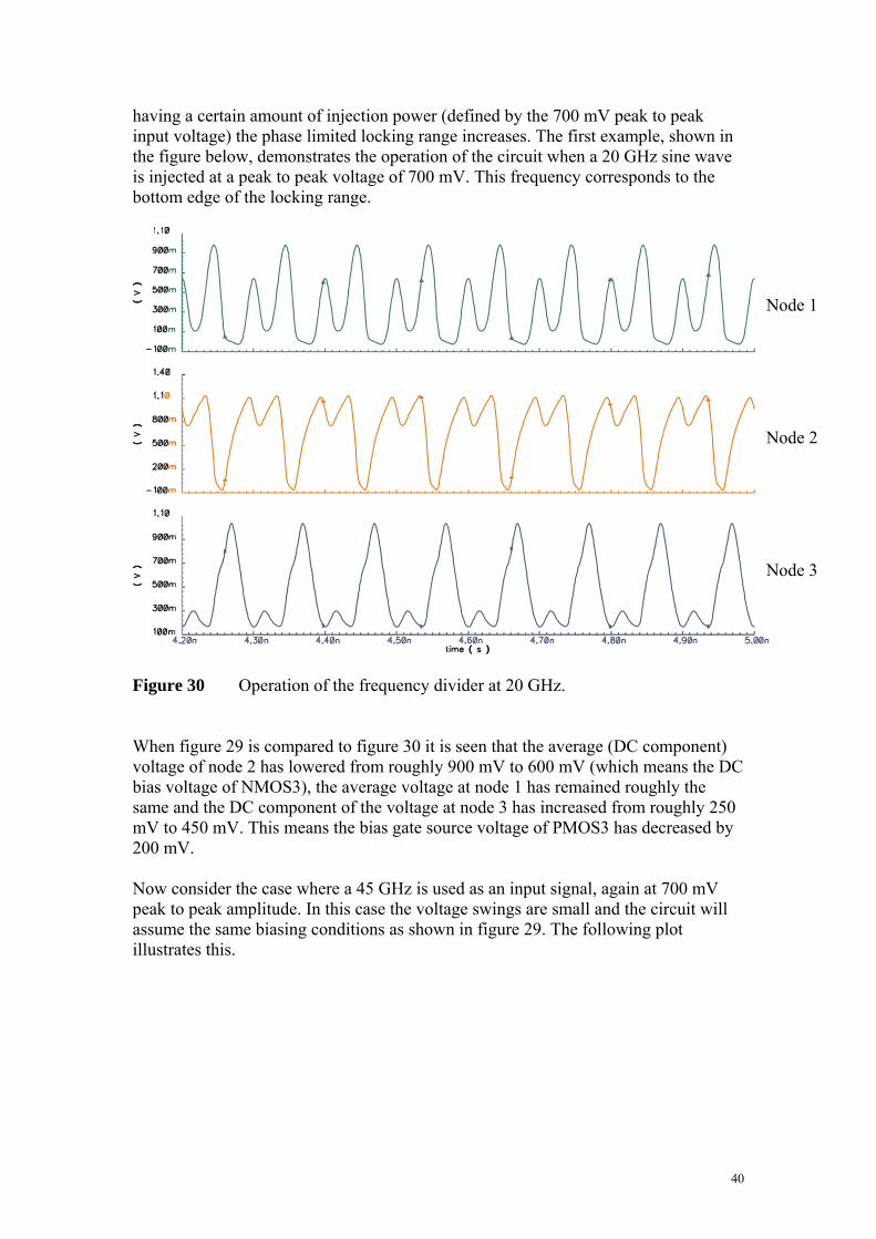
having a certain amount of injection power (defined by the 700 mV peak to peak input voltage) the phase limited locking range increases. The first example, shown in the figure below, demonstrates the operation of the circuit when a 20 GHz sine wave is injected at a peak to peak voltage of 700 mV. This frequency corresponds to the bottom edge of the locking range.
Figure 30 Operation of the frequency divider at 20 GHz. When figure 29 is compared to figure 30 it is seen that the average (DC component) voltage of node 2 has lowered from roughly 900 mV to 600 mV (which means the DC bias voltage of NMOS3), the average voltage at node 1 has remained roughly the same and the DC component of the voltage at node 3 has increased from roughly 250 mV to 450 mV. This means the bias gate source voltage of PMOS3 has decreased by 200 mV. Now consider the case where a 45 GHz is used as an input signal, again at 700 mV peak to peak amplitude. In this case the voltage swings are small and the circuit will assume the same biasing conditions as shown in figure 29. The following plot illustrates this.
Node 2
Node 1
Node 3

41
Figure 31 Operation of the frequency divider at 45 GHz. Figure 31 shows that the divider shown in figure 28 locks to 45 GHz just as it locks to 20 GHz. This indicates a locking range of 25 GHz, which is almost an improvement factor of 5 compared to the divider circuit shown in figure 22. It is clearly visible now that the voltage swings scales down as the input frequency increases. Because the voltage swings influence the voltage bias, this circuit can convert an incoming frequency to a DC voltage, and therefore it contains a form of FM frequency detection, as was discussed at the beginning of this paragraph. There is however 1 drawback. Because the voltage swing scales down at higher frequencies, the noise distance scales down proportionally. Additionally, the very asymmetric voltage shapes increase the amount of 1/f noise upconversion [6]. These problems will be dealt with in chapter 8 (Phase Noise). There is one element of optimization which has not been discussed yet, and this is the 2.18 kΩ resistor as shown in figure 28. This optimization is correlated to the gain condition which also has to be satisfied in order to support injection locking. Equation (41) shows the gain relation. Up till now this equation has not been discussed, because in the case of figure 22 when the voltage swings are always near the supply voltage, the total gain around the loop remains equal to 1; the nonlinear saturation part canceled out the linear gain of the system for the entire locking range (therefore the gain condition was always met). For the new divider shown in figure 28 this is however not the case. The gain relation will be repeated below.
( )ϕω cos2
31,11,032
1
222
KTKRGG
VRCV
in
ososcos +=− (47)
This gain condition can also be intuitively understood. The linear voltage gain around the loop is proportional to G3·R3. If this number increases, the non-linear gain K0,1 and
Node 2
Node 1
Node 3

42
the intermodulation coefficient K1.1 should decrease. In the circuit shown in figure 28 this is realized by slightly increasing the voltage swing (any voltage swing increase results in worse biasing conditions, which lowers gm hence lowers K0.1). In the divider circuit shown in figure 28 there is 1 resistor that can be varied. There is a minimum gain needed to sustain the proper operation of the circuit. This means that, given a certain Gm, if R is increased the gain limited maximum input frequency will increase. However, increasing R means increasing the output resistance of the 3rd ring oscillator stage. This means that the phase limited maximum input frequency will decrease. Intuitively, the value for R should be found at which both locking range edges (phase and gain limitation) fall on the same frequency; in this case the maximum frequency at which injection locking occurs is the highest. The following figure illustrates that the value for R should be 2.2 kΩ. Figure 32 Injection locking; depending on the value of R. The figure shows a very interesting phenomenon. The input to the frequency divider for this simulation was equal to 45.7 GHz, which is very accurately the edge of the locking range. At this frequency, when R is chosen too high (for instance 2.4 kΩ in the bottom plot of figure 32), the phase condition fails, and the circuit will exhibit ‘injection pulling’, as was discussed before. It can be seen by the bottom plot of figure 32 that a beat frequency exists. When R is chosen too low, the gain relation fails, as is shown in the top plot. It can be seen that a fin/2 component is present, but it dies out
R=2 kΩ
R=2.2 kΩ
R=2.4 kΩ
R=2.6 kΩ
43
relatively quickly because the loop gain is smaller than 1 for this frequency. Therefore, the circuit behaves as a stable feedback amplifier, which has its unity gain at a frequency at which there is not yet 2π of phase shift. This means that the locking range can be set to an optimum by choosing exactly the right value for R. While the phase limited locking range gets larger, the gain limited locking range gets smaller. The maximum locking range emerges when both locking ranges exactly overlap. The two middle plots in figure 32 show 2 cases where injection locking is just possible. It can be concluded in this paragraph that using an asymmetrical ring oscillator design enlarges the locking range as well as the maximum input frequency, when this ring oscillator is used as a frequency divider. There is one downside, and that is that because the output voltage swing scales down as the input frequency increases, the phase noise of the might divider increase. This is discussed in the next chapter.

44
8 Phase Noise
8.1 Introduction An important performance parameter for a frequency divider is phase noise. Like an oscillator, a frequency divider produces a periodic output signal. Noise sources within the frequency divider can momentarily perturb the phase of the periodic output signal. This process creates so called ‘phase noise’. An important aspect of this noise is that in the output spectrum it is situated closely around the signal frequency, and therefore options for filtering out this noise are very limited. In this chapter, first the time-variant phase noise theory for oscillators is discussed. After this an estimate for the phase noise of the ring oscillator as implemented will be given.
8.2 Time variant phase noise for a free running ring oscillator In this paragraph the time variant phase noise model as presented by Lee and Hajimiri [6] will be discussed shortly. The starting point is a free running ring oscillator. The reason a ring oscillator is considered is that the final design chosen in chapter 7 was a single ended 3-stage ring oscillator (which only had the one difference, which is that the NMOS in the first stage is the injection current source). Suppose a noise current impulse is injected onto a ring oscillator node:
( ) ( )τδ −= ttI (48) ( )tδ is the Dirac Delta function, the noise current impulse takes place at the moment
τ=t . The resulting voltage is:
( ) ( ) ( )CtHVdtt
CVtV ττδ −
+=−+= ∫ 001 (49)
In this equation ( )tH is the Heaviside step function, C is the total capacitance seen at the node and V0 is the voltage already present. Now suppose 0V is a periodic signal, from now on written as ( )tV0 which is given by:
( ) ( )tVtV 0max0 sin ω= (50) If ( )tV0 experiences a sudden voltage shift, its phase might also be perturbed. However the amount of phase shift caused by the current impulse depends on the moment τ. The following figure illustrates this.

45
Figure 33 Time dependence on amount of phase shift caused by current impulse. As can be seen in figure 23, if the current impulse happens when
( ) ( ) 0sinmax0 == tVtV ω the phase shift caused is maximum, while the same current impulse would not create any phase disturbance when ( ) ( ) max0max0 sin VtVtV == ω . This effect can be quantified using a so called ‘impulse sensitivity function’ or ISF. This function, designated ( )t0ωΓ , is periodic and has the same fundamental frequency as
( )tV0 . However the shape of the ISF also depends on the shape of ( )tV0 ; the output signal of an oscillator is not always a pure sine wave. Figure 24 shows the output signal shape and impulse sensitivity function for three types of oscillators. Figure 34 Impulse sensitivity functions for different types of oscillators. Figure 24 a, 24 b and 24 c respectively show ( )tV0 and ( )t0ωΓ for an LC-tank based oscillator, a relaxation oscillator and a typical ring oscillator. From (49) the voltage shift ΔV caused by the noise current impulse is derived:
( )CtHV τ−
=Δ (51)
This voltage shift can now be converted to a phase shift by taking into account both the impulse sensitivity function ( )t0ωΓ and the total voltage swing Vmax. Noting that when Vmax increases, the phase shift caused by δ(t) decreases and also noting that the larger the sensitivity ( )t0ωΓ , the larger the phase shift caused, the following response to the current impulse δ(t) can be written for the phase shift:
( ) ( ) ( ) ( )max
0
max0 Q
ttHCV
tHt ωττωϕ Γ−=
−Γ=Δ (52)
a) b) c)

46
In this formula Qmax is the maximum charge swing defined as CVmax and ( )τ−tH is the Heaviside step function. If a the noise present is given by a continuous function i(t) rather than a current impulse δ(t), the total noise response can be found by convolving this continuous function with the impulse response:
( ) ( ) ( ) ττωτϕ diQ
tt
0max
1Γ= ∫ ∞−
(53)
Because the impulse sensitivity function is periodic, it can be expanded in a Fourier series:
( ) ( )∑∞
=
++=Γ1
000 cosn
nn ncc θτωτω (54)
The phase constants nθ are not relevant as because the calculations here assume fully stationary random noise, and therefore the output phase can be written as
( ) ( ) ( ) ( ) ⎟⎠
⎞⎜⎝
⎛++= ∫ ∫ ∑∞− ∞−
∞
=
t t
nnn dnicci
Qt
100
max
cos1 τθτωττϕ (55)
That is, the impulse sensitivity function modulates incoming noise using carriers at frequencies nω0, and with coefficients cn. This modulation is visualized by the term
( ) ( )nn nic θτωτ +0cos . Because the modulation products get integrated, only the modulation products which have a frequency close to DC will be relevant; the high frequency components will be averaged out due to the integration. The time variable τ is from now on replaced with t, because this variable was only needed as a dummy for the convolution integral. Now for i(t) a periodic signal is assumed which has a frequency close to ω0 (i.e. Δω is small compared to ω0): ( ) ( )( )tnIti ωω Δ+= 0sin (56)
When substituting this value into (53), the output phase is found to be:
( ) ( )ωωϕ
ΔΔ
≈max2
sinQ
tIct n (57)
In this equation, it is seen that only the coefficient cn is used, because only this modulation product is situated close to DC. Using the approximation that
( ) ( )( ) ( ) ( ) ( )tttttItV 000 sincoscos ωϕωϕω +≈+= the oscillator output voltage can be expressed as:
( ) ( ) ( ) ( )tQ
tIcttV n0
max0 sin
2sincos ω
ωωω
ΔΔ
+≈ (58)
From this output, the noise component (which is the second term in the right hand equation) can be rewritten as:
( ) ( ) ( )( ) ( )( )( )ttQ
IctQ
tIc nn ωωωωω
ωωω
Δ++Δ−Δ
=ΔΔ
00max
0max
sinsin4
sin2
sin (59)
The power of this noise component with respect to the signal ( )t0cos ω is
( ) 22
222
max max42 ωω
ωΔ
=⎟⎟⎠
⎞⎜⎜⎝
⎛Δ
=ΔQ
IcQ
IcP nnnoise (60)
This equation states that the power of the noise decreases with the square of Δω. However, this equation only shows the output noise as a consequence of the coefficient cn. When instead of a periodic noise signal with a frequency close to 0ωn , a white noise source is assumed, (60) can be rewritten as:
47
( )( )
22
2
0
2
max4 ω
ωΔ
Δ=Δ∑
∞
=
Q
cf
i
P nn
noise
n
(61)
Here the noise amplitude I from equation (59) has been replaced with the spectral noise power density and because white noise consists of all frequencies, all modulation product coefficients are included. Parseval’s theorem states that
( ) ∑∫∞
=−
=Γ=Γ0
2220 21
nnrms cdττω
ππ
π (62)
Using Parsevals’s theorem, (61) can be rewritten as:
( ) 22
22
max2 ω
ωΔ
ΓΔ=ΔQ
fi
Prms
noise
n
(63)
The spectral noise power density is build up by 2 components; the thermal noise coming from resistors and transistors as well as 1/f noise (flicker noise) from the transistors. The thermal noise from a resistor can be evaluated as
ktRf
in 42
=Δ
(64)
where R is the resistor value, k is Boltzmann’s constant and t is the absolute temperature. The thermal noise and flicker noise from the transistors can be evaluated by using the program ProMOST. The impulse sensitivity function can be evaluated by observing the waveforms at every ring oscillator node in the time domain. There is no closed form expression for this impulse sensitivity function if the waveforms are very specific. For a symmetrical ring oscillator, the ISF has been derived in closed form by literature [6] to be:
5.1
2 13
2Nrms η
π=Γ (65)
In this formula η is a proportionality constant (usually close to unity). However because of the very asymmetric nature of the ring oscillator as chosen in chapter 7, a closed form formula like (65) can not be used. The last remark made about phase noise calculation for the free running ring oscillator is that the noise has to be calculated for every single node. Because the noise sources of the nodes are uncorrelated, their powers are added. In order to find out the order magnitude of the phase noise, number will be used to fill out (63)

48
For every ring oscillator node, 6.0=Γrms . The spectral noise component f
in
Δ
2
can be
evaluated from ProMOST; for a 3/0.1 dimensioned NMOS transistor (which is taken as average for simplification) biased VDS = VGS = 0.6 is equal to 5.5 pA/sqrt(Hz) or 3e-23 A2/Hz. When filling in Qmax = 2.5e-15*1.2 and Δω = 6.2e9 radians per second, the value for (63) is equal to:
( )( ) ( ) dBcPnoise 13814exp57.19exp2.6 −=−==Δω This is the noise contribution of 1 noise source. There are 5 transistor noise sources which contribute thermal noise and also a resistor. The thermal noise for a 2.2 kΩ resistor equals 3.5e-17 V2/Hz = 6.4e-23 A2/Hz which gives a phase noise of – 135 dBc at an offset of 6.2e9 radians = 1 GHz. Therefore the assumption is that the total noise at an offset of 1 GHz is roughly equal to 130 dBc/ Hz. The following plot shows the phasenoise, and at an offset of 1 GHz (which is in the 1/f2 region) this noise is roughly equal to 120 dBc.
8.3 Simulation results
Figure 35 Phase noise plot, phase noise as function of the injected power. In this plot the top graph is the phase noise for the free running oscillator. This plot shows a strong upconversion of 1/f noise, which can be explained by stating that the DC component of the Impulse Sensitivity Function is relatively high [6]. This is a disadvantage of the asymmetrically implemented ringoscillator. The plots underneath
Free running oscillator
Injection at -10.7 dBm
Injection at -49 dBm

49
the free running plot in figure 35 show the phase noise at 30 GHz injection for various injection powers. The bottom plot corresponds to an input voltage of 700 mV peak to peak into the divider, which is a blind power of 10.7 dBmW. The weakest injection power at locking is -49 dBmW and the phase noise plot for this is indicated in figure 35. All other plots are values in between. As can be seen, the 1/f3 slope of the free running phase noise plot has been repressed to a 1/f slope in all injection locked cases. This is because the noise passes through a ‘high pass noise transfer function’ that has a -1/f2 slope which starts at a certain frequency ωp which is determined by the phase limited locking range of the divider [7]. The ‘peaks’ in the phase noise plot around 13 GHz shown the first harmonic, and its own surrounding phase noise. Important also is the injection locking at higher frequencies than 30 GHz. Because in chapter 7 it was simulated that the voltage swings reduce to less than 150 mV peak to peak in the oscillator, the phase noise will increase because the power of the noise sources does not attenuate when the injected frequency increases. The following plot shows, the phase noise at several injection frequencies (all simulations were done at 700 mV peak to peak input voltage swing into NMOS1). Figure 35 Phase noise as a function of injection frequency. This plot shows (from top to bottom) the phase noise plot for 45.7, 45.6, 45, 44, 42.5, 41.5, 40, 35 and 30 GHz input frequencies respectively. As can be seen, the frequencies from 45.7 till roughly 45 GHz suffer from substantial phase noise. At 44 GHz, the phase noise at 1 MHz offset is about -105 dBc, which is just 15 dB ‘worse’ than the injection at 30 GHz (-120 dBc at 1 MHz offset). Therefore it can be concluded that phase noise needs not be a problem in this design; it consumes about 1.44 mW, therefore the transistors could be sized up (and the resistor sized down) at the cost of more power consumption to reach the same phase noise as the other frequency dividers have (see chapter 9) while keeping the high locking range.

50
9. Divider Performance and Benchmarking In this chapter the performance parameters will be evaluated of the frequency divider that is proposed (this divider is shown in figure 28). Static dividers will not be included in the comparison, because they either operate at much lower frequencies or consume much more power than the divider discussed in this report. Furthermore, only CMOS process based frequency dividers are considered. Very fast HEMT technologies or bipolar technologies based dividers cannot be integrated in a on-chip CMOS PLL solution, and these technologies are generally faster than standard CMOS. It should be noted that all values from this work are simulated values; actual performance will decrease because the divider has to be loaded at the output (simulated degradation in maximum input frequency is roughly 1 GHz), wiring capacitances are not included, supply phase noise has not been included in the simulations and transistor mismatch can also influence the phase noise performance. The other values of other work are measured values.
Used power
Maximum input frequency
Lock. range
Phase noise /Hz (offset)
Die size (mm2)
Coils (Y/N)
CMOS technology (year)
Injection power required
Div. ratio
T. Lee [7] N/A 5.4 GHz 300 MHz
-115 dBc (0.1 MHz)
0.189 Y 240 (2003)
0 dBmW 2
Betancourt-Zamora [8]
0.35 μW 2.8 GHz 20 MHz
-110 dBc (0.1 MHz)
0.012 N 240
N/A 8
Razavi, [9] 31 mW 40.6 GHz 2.3 GHz
-115dBc (1 MHz)
0.35 Y 180 nm (2004)
3-4 dBmW
4
Liang-Hung Lu [10]
23.8 mW 46.9 GHz 5.7 GHz
-103.1 dBc (1MHz)
0.56 Y 180 nm (2005)
4
Wei-Zen Chen and Chien-Liang Kuo [11]
1.75mW 18 GHz 10 MHz
-101dBc (0.1 MHz)
2.2 Y 250 3.5 dBmW
5
This work 1.44 mW 36 GHz 12 GHz
-110 dBc (0.1 MHz)
N/A N 90 (2006)
-10 dBmW
2
The die size of the proposed frequency divider is not large; the circuit contains 5 transistors (the largest of which is 5/0.1 μm) and one 2.18 kΩ resistor. Injection power required for the proposed divider includes the blind current into the 2.5 fF capacitor seen at the input of the divider. At 36 GHz the simulated blind current is 0.24 mA RMS. This corresponds to a blind power of 0.084 mW which is roughly -10 dBmW.

51

52
10. Conclusions
1. In this report the possibilities of a frequency divider which is based on charging and discharging a capacitor has been investigated. Initially the goal was to investigate if the potential of transistors to almost infinitely fast convert a voltage to a current, can be used to bypass the inherent transit frequency limitation that transistors have. Several circuit topologies have been analyzed; ultimately this resulted in an implementation in which a form of a ringoscillator is used as an injection locked frequency divider. The design process has basically led to an oscillatory system which is speed limited by the transit frequency of the transistors. 2 important reasons can be given for this.
a. At very high frequencies no way has been found to ‘temporarily open’ an otherwise closed loop of amplifier stages. This loop is inherently present in the charge / discharge model because the discharge circuit has its input and its output connected to the capacitor. This leaded to an oscillatory system because the only way found to create a ‘new’ frequency from a closed loop of amplifier stages is to use this loop as an oscillator.
b. Time variant systems are possible such that the loop is temporarily opened. One example of this has been investigated; this was the mono-stable circuit, which showed that in order to reach the time variance the maximum input frequency will be relatively low compared to the maximum input frequency into an injection locked frequency divider. Because no other time variant circuit was found that behaves at very high speeds compared to an oscillator, the oscillator topology was chosen.
2. A power and die size efficient way to implement a frequency divider based on charging and discharging a capacitor is a modified single ended 3 stage ring oscillator. The modification is that one stage of the ring oscillator is only connected to the foregoing stage through its PMOS transistor. The gate of the NMOS transistor of that stage can be used to inject a sine wave voltage at a certain frequency. The total die size only consists of 5 transistors and 1 resistor, consuming roughly 1.44 mW from a 1.2 V supply.
3. If the ring oscillator used as a frequency divider is implemented in an asymmetrical way the different nodes of the oscillator have different bias voltages. These bias voltages depend on the frequency of the incoming signal. This way it is possible to extend the locking range of the frequency divider without increasing the injection power.
4. The implemented asymmetrical ring oscillator will suffer from upconversion of 1/f noise. This creates substantial phase noise, if the oscillator runs free without any injection current. The amount of phase noise however decreases once the oscillator locks onto the injected signal for frequency division. Even for high injection frequencies, the phase noise remains ‘acceptable’ when compared to other frequency dividers.
5. Because no external components like an LC-tank or additional RC-circuitry has been used, because the intention is not to use coils in the design due to the amount of die space needed and due to the fact that additional RC-circuitry would mean lower input and output voltages, the actual speed of the circuit is very dependant on the transistor parameters and therefore very sensitive to process spread; wafer to wafer process spread as well as transistor mismatch.

53
This implies the locking range should be relatively large in order to be certain that no matter what the transistor parameters are, a certain ‘effective locking range’ is always guaranteed. This effective locking range can be defined as the ‘overlap’ between the locking range when the transistors are modeled as ‘fast’, and the locking range corresponding to ‘slow’ transistors. The words ‘fast’ and ‘slow’ are based on the CMOS process libraries used in Cadence, which cover a 3σ spread of all devices. The effective locking range of the proposed divider is roughly 12 GHz, and lies in the range 24 – 36 GHz.
6. Frequency division ratios higher than 2 are not supported by this injection locked frequency divider. The reason for this is that the process variations cause the locking ranges of division ratios higher than two to shift so much that the effective locking range equals zero.

54
↑I2(t) VC (t)
Cgate
I1(t) gm
( ) ( )
C
dttItItV
t
C
∫∞−
−=
21
)(
( ) mC gtVtI *)(2 =
11. Appendix A This appendix shows that a single transistor cannot be used as an implementation for the discharge circuit, which is a part of the conceptual frequency divider shown in figure A-1. The aim is to shown that the incoming frequency will not be divided by this circuit. The response of the circuit shown in figure 7 (this figure is redrawn below in figure A1) will be derived. This circuit can be described with two relations (A-1) and (A-2)
(A-1) (A-2)
Figure A-1 First implementation of discharge circuit. The NMOS transistor will be modeled as a linear transconductance with a threshold voltage Vt. This means that for 0 < VC(t) < Vt the transconductance of the transistor is 0. For VC(t) > Vt, the transconductance is given by a positive constant gm and the system will become a 1-pole linear system exited with a square wave current. The response of the circuit looks like this: Figure A-2 Qualitative behavior of the circuit shown in figure A-1.
Until the threshold voltage Vt, C charges according to C
tItVC*)( 1= . The following
analysis assumes that VC(t) > Vt. In the figure the periods P1, P2, P3 and P4 are defined. These will be used in the analysis. Every period has a length of T (this means that T = Tin/2). Substituting (A1) in (A2) yields the following differential equation:
Vt
Tin
I2(t)
VC(t)
I1(t)
0
0
V↑
I↑
I↑
P1 P2 P3 P4
1I

55
( ) ( )m
t
t
gC
dttItItI *)(
2
2
∫∞−
−= ( ) ( )tItI
ttI
gC
m21
2 )(−=
∂∂ (A-3)
When ( ) 11 ItI = (which happens during P1, and P3 see figure A-2) the following holds:
( )tIIttI
gC
m21
2 )(−=
∂∂ , ( ) 02 0 WI = (A-4)
In (4) W0 is an initial condition for the current I2. This initial condition equals zero at the beginning of P1 but is at the beginning of P3 this is not the case. The solution to this differential equation is:
( ) ( ) ⎟⎠⎞
⎜⎝⎛−−+=
CgtIWItI m*exp1012 (A-5)
This gives the following expression for the I2 at the end of P1:
( ) 11012*exp WC
gTIWII m =⎟⎠⎞
⎜⎝⎛−−+= (A-6)
When T goes to infinity, 2I will become equal to 1I . When T is a finite number,
11 WI > . This value is the initial condition for the differential equation which holds during P2:
( )tIttI
gC
m2
2 )(−=
∂∂ , ( ) 12 0 WI = (A-7)
This can be solved as:
( ) ⎟⎠⎞
⎜⎝⎛−=
CgtWtI m*exp12 (A-8)
This gives the following expression for I2 at the end of P2:
212*exp WC
gTWI m =⎟⎠⎞
⎜⎝⎛−= (A-9)
The signal I2(t) becomes steady state after an infinite amount of periods. This steady state can be calculated by stating that W2 = W0 should hold for this steady state. The
factor ⎟⎠⎞
⎜⎝⎛−
CgT m*exp is equal in both (A-6) and (A-9), it is considered a constant from
now on called F. This creates the following equation system: FWW *10 = (A-10) ( )FIWIW 1011 −+= (A-11)
Solving this system yields:
11
210 −−
=FFFIW (A-12)
11
211 −−
=FFIW (A-13)
Furthermore: ( )( )
121212101 111
11
11 I
FFFI
FFFI
FFIWW =
−−+
=−−
+−−
=+ (A-14)
Substituting this gives the solution for I2(t) in the steady state.

56
( ) ⎟⎠⎞
⎜⎝⎛−
⎟⎟⎟⎟
⎠
⎞
⎜⎜⎜⎜
⎝
⎛
−−⎟
⎠⎞
⎜⎝⎛−
−⎟⎠⎞
⎜⎝⎛−
⎟⎠⎞
⎜⎝⎛−+=
CgtI
CgT
CgT
CgTIItI m
m
m
mPn
*exp1*2exp
1*exp*exp 1112 (A-15)
The expression for I2(t) during I1(t) = 0 is:
( ) ⎟⎠⎞
⎜⎝⎛−
−⎟⎠⎞
⎜⎝⎛−
−⎟⎠⎞
⎜⎝⎛−
=+ Cgt
CgT
CgT
ItI m
m
m
Pn*exp
1*2exp
1*exp112 (A-16)
Pn and Pn+1 are the steady state periods; during Pn ( ) 11 ItI = , and during Pn+1 ( ) 01 =tI . These two expressions do not include any initial conditions and are only dependant on the parameters T, gm, 1I and C. This indicates the system will assume a steady state, where in the periods Pn and Pn+1 . But how will the system attain this steady state? This can be derived from the average current I2/2 which goes into the 1-pole system which is described by the following differential equation:
( ) )(2
)(2
12 tItIttI
gC
m
−=∂
∂ (A-17)
This equation has an initial condition I2(0) = Y. Here Y is the initial current into the system. The solution to this equation is the envelope of the periodic signal:
( ) ⎟⎠⎞
⎜⎝⎛−⎟
⎠⎞
⎜⎝⎛ −+=
CgtIYItI m
envelope*exp
221
01
2 (A-18)
The voltage across the capacitor can now easily be derived by the relation:
( ) thm
C Vg
tItV +=)(2 (A-19)
This analysis predicts the behavior as shown in the following figure, which shows that no frequency division takes place. This behavior is verified using Matlab Simulink. A matlab simulink model of the system looks like this: Figure A-3 Simulink model of the circuit shown in figure A-1. Here the combination of the blocks “relay” and “product” (visible in the bottom of figure A-3) and the block “constant” emulate a threshold voltage of 0.4 volts. This model has a capacitor of 1 farad and an input current I1 = 1 A, having a period of 2 seconds, in this case T = 1. gm is defined as log(2). The result expected from the analysis is that W0 = 1/3, W1 = 2/3, the average current through the capacitor is ½ A. This means the current amplitude would be 1/3 with an offset of ½ A. The voltage

57
amplitude = 1/3·(1/log(2)), the offset is 0.4+1/2·(1/log(2)). The plot from the Matlab scope is shown below (top plot = current, bottom plot = voltage). Figure A-4 Simulated behavior of the circuit shown in figure 7. This clearly shows a 1-pole system will not function as a frequency divider; there is no frequency component present at the output that is lower than the input frequency.

58
12. Appendix B In this appendix the mono-stable circuit is analyzed, the conclusion of this appendix is that a mono-stable circuit can be used in a frequency divider system, however the maximum input frequency is very limited. The mono-stable circuit was mentioned in chapter 5 as a potential way of creating the time variant behavior needed for the discharge circuit to function properly. The goal of the mono-stable circuit is to create a pulse with a constant and predetermined duration, when the input of the circuit exceeds a certain voltage threshold. Before the mono-stable circuit is discussed, a well known circuit topology is the so-called ‘bi-stable’ circuit is discussed first. This is essentially a cross-coupled latch. The following figure shows the basic topology of a bi-stable circuit: Figure B-1 Example of bi-stable circuit. The bi-stable circuit can assume 2 ‘stable’ states. Either N0 is off and N1 is on, which means that V0 is high and V1 is low, or N1 is off and N0 is on (which is the opposite state). These states are ‘stable’ in a sense that the circuit holds this state indefinitely. It forms the basis of the ‘latch’, i.e. the memory element in digital circuits. This circuit can be modified such that has only 1 stable state; this modified circuit is shown in the following figure: Figure B-2 Mono-stable circuit. The element in figure B-2 that makes the circuit ‘mono-stable’ is the series resistor combination R2/R3. Now consider the following inequality.
Vin
Vout
N1 N2N3
R3
R4R2R1 C1
V1V0
V1
N0 N1
V0

59
3,32
31 NthDD VV
RRRV >+
= (B-1)
That is, if the voltage at V1 exceeds the threshold voltage of N3, the stable condition is Vout = low, V0 is high, N3 is on, and both N1 and N2 are off. It will now be explained how the mono-stable circuit works. The goal of the mono-stable circuit is to produce a pulse with duration T2 at the output, when a pulse having a minimum duration of T1 is present at the input. The following steps explain qualitatively how this circuit works:
1. This circuit initially is in its stable condition; N1 and N2 are off, N3 is on, Vout is low (almost at GND) and V0 is high (almost equal to VDD). There is no voltage across C1 (in this state the difference between V0 and V1 = VDD·R2/R3 is neglected, C1 is discharged).
2. When a short input pulse of duration T1 is applied to the input, N1 temporarily turns on, pulling down V0. Because C1 cannot instantly charge, V1 is also pulled down and turns N3 off.
3. Now the inverse of the stable state occurs; Vout becomes high and V0 is low. This subsequently means that N2 is also switched on, pulling down V0.
4. At this moment both N2 and N1 are on, and if the incoming pulse ends (i.e. if the input becomes low again) V0 remains pulled down by N2.
5. As soon as V0 is pulled down (initially by N1, and later by N2), C1 starts charging through the R2/R3 combination such that after a certain amount of time V1 exceeds the threshold voltage of N3 again; at this moment the voltage across C1 is equal to Vth,N3.
6. When this happens, the output becomes ‘low’ and the output pulse ends. 7. At that same moment, N2 turns off and V0 pulls up to VDD. This means V1
gets pulled up to a value of V0 + VC1 = VDD + Vth,N3. 8. In order to reach the initial stable condition as explained in step 1, C1 must be
discharged such that V1 equals VDD·R3/(R2+R3) again. This discharge time is equal to the charge time mentioned in step 5.
The following steps indicate the minimum time T1 needed to make sure that transistor N2 gets turned on. This minimum time In the following analysis, when V0 is pulled to ground it is assumed V0 = 0 for simplification. Furthermore it is assumed that when N1 and N2 are off, V0 equals V1. The voltage V1 is a function of time as soon as V0 gets pulled to ground:
( ) ( )⎟⎟⎠
⎞⎜⎜⎝
⎛⎟⎠⎞
⎜⎝⎛ +−−=
1*3*232*exp1
32
1 CRRRRt
RRVtV DD (B-2)
This equation describes the charging of C1 from 0 towards VDD·R2/R3 witch a time constant C1·(R2||R3). An important assumption is made here. It is that the transistors N1 and N2 form a negligible resistance when C1 charges or discharges. The time T2 now follows from equating this to the threshold voltage of N3 (at that moment, the output voltage becomes ‘low’ again and the pulse ends):
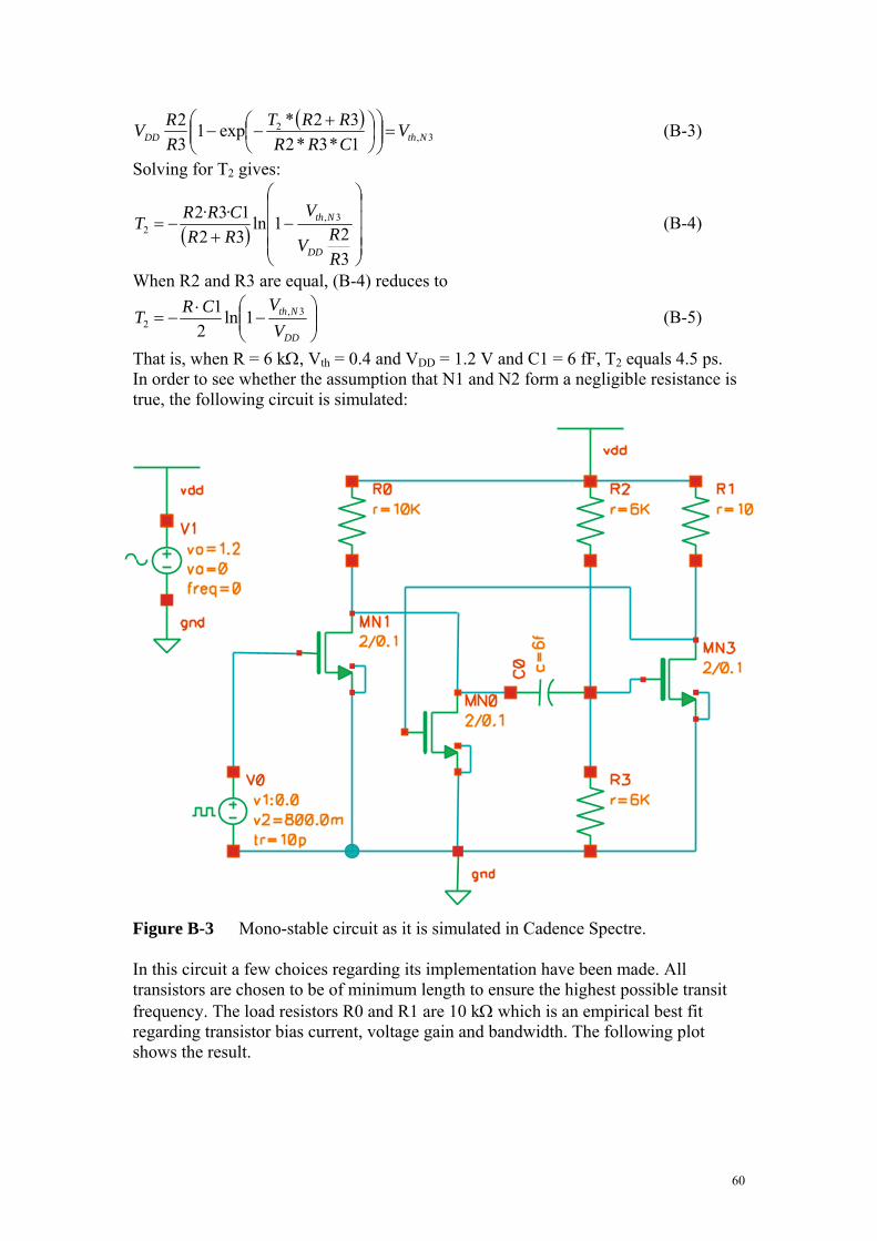
60
( )3,
2
1*3*232*exp1
32
NthDD VCRRRRT
RRV =⎟⎟
⎠
⎞⎜⎜⎝
⎛⎟⎠⎞
⎜⎝⎛ +−− (B-3)
Solving for T2 gives:
( )⎟⎟⎟⎟
⎠
⎞
⎜⎜⎜⎜
⎝
⎛
−+
−=
321ln
321·3·2 3,
2
RRV
VRRCRRT
DD
Nth (B-4)
When R2 and R3 are equal, (B-4) reduces to
⎟⎟⎠
⎞⎜⎜⎝
⎛−
⋅−=
DD
Nth
VVCRT 3,
2 1ln2
1 (B-5)
That is, when R = 6 kΩ, Vth = 0.4 and VDD = 1.2 V and C1 = 6 fF, T2 equals 4.5 ps. In order to see whether the assumption that N1 and N2 form a negligible resistance is true, the following circuit is simulated: Figure B-3 Mono-stable circuit as it is simulated in Cadence Spectre. In this circuit a few choices regarding its implementation have been made. All transistors are chosen to be of minimum length to ensure the highest possible transit frequency. The load resistors R0 and R1 are 10 kΩ which is an empirical best fit regarding transistor bias current, voltage gain and bandwidth. The following plot shows the result.
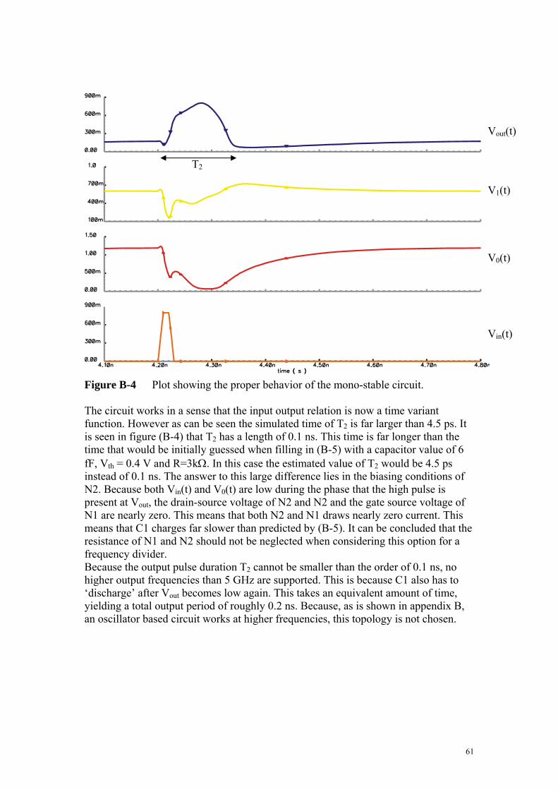
61
Figure B-4 Plot showing the proper behavior of the mono-stable circuit. The circuit works in a sense that the input output relation is now a time variant function. However as can be seen the simulated time of T2 is far larger than 4.5 ps. It is seen in figure (B-4) that T2 has a length of 0.1 ns. This time is far longer than the time that would be initially guessed when filling in (B-5) with a capacitor value of 6 fF, Vth = 0.4 V and R=3kΩ. In this case the estimated value of T2 would be 4.5 ps instead of 0.1 ns. The answer to this large difference lies in the biasing conditions of N2. Because both Vin(t) and V0(t) are low during the phase that the high pulse is present at Vout, the drain-source voltage of N2 and N2 and the gate source voltage of N1 are nearly zero. This means that both N2 and N1 draws nearly zero current. This means that C1 charges far slower than predicted by (B-5). It can be concluded that the resistance of N1 and N2 should not be neglected when considering this option for a frequency divider. Because the output pulse duration T2 cannot be smaller than the order of 0.1 ns, no higher output frequencies than 5 GHz are supported. This is because C1 also has to ‘discharge’ after Vout becomes low again. This takes an equivalent amount of time, yielding a total output period of roughly 0.2 ns. Because, as is shown in appendix B, an oscillator based circuit works at higher frequencies, this topology is not chosen.
Vin(t)
Vout(t)
V1(t)
V0(t)
T2

62
13. Appendix C This appendix deals with the linear behavior of a ring oscillator. The ring oscillator can be described by the linear model shown in figure C-1 Figure C-1 Linear version of ring oscillator circuit. For every stage of a ring oscillator the transfer between input voltage and output voltage can be written as
RCjRg
CjRg
VV outm
outmout
in
ωω +=⎟⎟
⎠
⎞⎜⎜⎝
⎛⋅=
1*1|| (C-1)
The argument of this complex number is the phase shift caused by one stage: ( )RCωϕ arctan−= (C-2)
3 stages of this ring oscillator should provide a phase shift of π radians (the net inversion around the loop creates an additional π radians, such that the total phase shift around the loop is equal to 2π). Assuming all stages of the loop are identical the following holds:
( )RCωπ arctan3−= (C-3) This means that the frequency of oscillation can be given by [1]:
RCRCfosc ππ
π
23
23
tan=
⎟⎠⎞
⎜⎝⎛ −
= (C-4)
In order for oscillation to occur, the loop gain should be at least unity. If all stages are identical this means that the absolute value of (C-1) should be at least unity, which means that
2221 CRRg outm ω+≥ (C-5) If all stages are equal, it follows that 2≥outmRg . Assuming the loop gain is larger than 1, the voltage swing will keep growing until it saturates due to non-linear amplitude limiting. This amplitude limiting will create a nonlinear form of oscillation. Because the resulting voltage swing is very large, the
-Gm
-Gm
-Gm
n1 n2 n3

63
parameters gm, Rout and Cin (which determine the loop gain and phase shift of the ring oscillator) are very hard to evaluate. In spite of this, an attempt is made to evaluate the oscillation frequency of the ring oscillator. The following table will show for a PMOS and NMOS device having dimensions 3/0.1 in a C090 technology the output resistance Rout, the gate capacitance Cin and the transconductance gm. NMOS PMOS
|VDS| = 200mV
|VDS| = 600 mV
|VDS| = 1V
|VGS| = 200 mV
10MΩ, 1.4fF, 1.0μS 11MΩ, 1.0fF, 0.84μS
5.7MΩ, 1.4fF, 2.4μS 5.4MΩ, 1.0fF, 2.3μS
2.8MΩ, 1.4fF, 5.3μS 2.8MΩ, 0.96fF, 4.7μS
|VGS| = 600 mV
4.5kΩ, 2.5fF, 1.2mS 11kΩ, 2.1fF, 0.4mS
8.0kΩ, 2.5fF, 1.5mS 17kΩ, 2.0fF, 0.56mS
8.0kΩ, 2.5fF, 1.7mS 17kΩ, 1.9fF, 0.65mS
|VGS| = 1 V
0.5kΩ, 3.4fF, 1.4mS 1.2kΩ, 2.7fF, 0.38mS
3.0kΩ, 2.8fF, 2.2mS 4.6kΩ, 2.3fF, 0.93mS
4.2kΩ, 2.8fF, 2.3mS 6.9kΩ, 2.2fF, 1.1mS
Table C-2 Different values for Cin of a PMOS or NMOS transistor determined by biasing conditions (unit = Farad).
Because both the input and the output of every stage in a ring oscillator has the large voltage swing, all 3 parameters Rout, Cin, and gm vary, making it very hard to approximate the oscillation frequency using linear analysis. Furthermore, process waver to wafer variations can cause variations in transistor properties, these properties are therefore bound to a normal distribution. When evaluated using PROMOST, a range of 3σ corresponds to a rough 15% variation in transconductance and input capacitance and about 30 % variation in output resistance. Considering table C-2, and assuming that a full sine wave of 1.2 V amplitude and 0.6 V offset spends 44% of the time in the region 800-1200 mV and the same amount of time in the 0-400 mV region, the transconductance of a 3/0.1 NMOST could be averaged to about 1-1.5 mS. The capacitance of the same transistor seen at the gate would be 2.5 fF and the output resistance would equal 6 kΩ Linear interpolation can be used for transistors with other dimensions, that means that for instance the transconductance of an 2/0.1 NMOS would equal 0.66 – 1 mS. The same applies for a resistor; 6 kΩ output resistance for a 3/0.1 NMOS means 9 kΩ output resistance for a 2/0.1 NMOS transistor. For the PMOS, the gm can be equal to 0.35 times the gm of an NMOS transistor. When an NMOS and PMOS transistor have equal dimensions the relation for the output resistance can be approximated by Rout,PMOS = 2 Rout,NMOS An equivalent rule applies for the gate input capacitances; Cin,PMOS = 0.8 Cin,NMOS

64
14. Appendix D This appendix shows the correlation between the intermodulation coefficient K1,1 and the second order harmonic coefficient a2 as defined in (23). The two sinewaves VA and VB are defined as:
( ) ( )tVGZtV osmA ωψ cos11= (D-1) ( ) ( )ϕωξ += tVGZtV ininmB cos_1 (D-2) ( ) ( ) ( )tVtVtV AB 1=+ (D-3)
ξVGZA inm _1= (D-4)
ψVGZB m11= (D-5) When the sum of ( )tVB and ( )tVA is at the input of the nonlinear function (23) and if only 2nd order harmonic distortion is evaluated, the output of the non-linear function is:
( ) ( )( ) ( ) ( )( ) ( ) ( )( )221 coscos*coscos*coscos tBtAatBtAatBtAf osinosinosin ωωωωωω +++=+
The second order term can be rewritten as ( ) ( )( ) ( ) ( )( ) ( ) ( )ttABatBtAatBtAa osinosinosin ωωωωωω coscos2coscos*coscos* 2
222
22 ++=+
Rewriting the intermodulation product gives: ( ) ( ) ( )( ) ( )( )( )ttABattABa oscinjoscinjoscinj ωωωωωω ++−= coscos2coscos2 22 (D-7)
From this intermodulation product, the high frequency term ( )( )toscinj ωω +cos will be filtered out and therefore the intermodulation term can be written as
( )( ) ( )ttVVGGZKtABa osinminmoscinj ωωωω ψξ −=− cos21cos 1_
211,12 (D-8)
This means that for K1,1 the following can be written: 21,1 *2 aK = (D-9)

65
15. References [1] R. L. Miller, “Fractional-frequency generators utilizing regenerative
modulation,” Proc. Inst. Radio Eng., vol. 27, pp. 446–456, July 1939. [2] R. Adler, “A study of locking phenomena in oscillators,” Proc. Inst.
Radio Eng., vol. 34, pp. 351–357, June 1946. [3] Razavi, “Design of Analog CMOS Integrated Circuits”, 2001. [4] H. R. Rategh and T. H. Lee, “Superharmonic injection-locked frequency
dividers,” IEEE J. Solid-State Circuits, vol. 34, pp. 813–821, June 1999. [5] Razavi, “A study of injection Locking and Pulling in Oscillators”, IEEE J.
Solid-State Circuits, vol. 39 pp 1415-1424, September 2004. [6] Hajimiri, A., Lee, T.H, “The Design of Low Noise Oscillators” 1999 [7] Hajimiri, A., Lee, T.H, “A Unified Model for Injection Locked Frequency
Dividers”, IEEE J. Solid-State Circuits, vol. 28 no. 6 pp 1015-1027, June 2003.
[8] R.J. Betancourt-Zamora, Shwetabh Verma and Thomas H. Lee, “1 GHz and 2.8 GHz CMOS Injection Locked Ring Oscillator Prescales”
[9] B. Razavi, “A 40 GHz Frequency Divider in 0.18 μm CMOS Technology”, IEEE J. Solid-State Circuits, vol. 39 pp 594-601, April 2004
[10] Liang-Hung Lu and Jun-Chau Chien,”A Wide-band CMOS Injection-Locked Oscillator”, J. Solid-State Circuits, vol. 15 pp 676-678, October 2005
[11] Wei-Zen Chen and Chien-Liang Kuo, “18 GHz and 7 GHz Superharmonic Injection-locked Dividers in 0.25 μm CMOS Technology”

66