faculty of engineering sciences department of electrical and computer...
TRANSCRIPT

��
��
Faculty of Engineering Sciences
Department of Electrical and Computer Engineering
MicroProcessor Based System Design
Advanced Micro-Computers Laboratory
Combined Project 2nd Semester 2003��
Implementing “Sheep And Wolves” with:
HC11 Micro Controller FLEX10K FPGA VGA Display EVBGU’s KeyBoard, LCD, PAL & RAM
By : Idan Tavor Maoz Barda
Microprocessor Based System Design lecturer: Mr. Isacc Hadad
Advanced micro lab instructor: Mr. Alex Reizenson
Table of contents :
Chapter 1 – The combined System
1.1 – Project’s Overview 1.2 - System’s description 1.3 – Hardware Block Diagram Chapter 2 – The HC11 Based System 2.1 – Program Flow 2.2 – Subsystems description 2.3 – Timing diagrams Chapter 3 – The FLEX10K FPGA roll 3.1 – Overview 3.2 – Modules and Hierarchies Appendix A - Pin Connection Diagram Appendix B – HC11 Assembler source code Appendix C – PAL Programming Appendix D – FPGA Verilog source code Appendix E – VGA Driver Operation

Chapter 1 – The combined System 1.1 Project’s overview This Implementation of “Sheep and Wolves” game is a final project for two courses: “Microprocessor based system design” “Advanced Microcomputers Laboratory” Which were taken in 2nd Semester, 2003. The different prospectives of each course made the project more of a “technological demonstrator” than an easy-to-use, commercial game. The game is simple. The player controls a sheep (shown as a chess horse tool) and his goal is penetrating the 4 wolves (controlled by software and shown as chess soldiers) line. The wolves’ objective is to encircle the sheep to the point it cannot move anymore. The moves are taken by turn and the sheep and wolves can travel only from one blue square to its neighbor blue square. The sheep can travel both forward (up) and backward (down) and the wolves can travel only forward (down) on diagonal lines.
Controlling the sheep is made with the EVBGU Keyboard and feedback is shown on the EVBGU LCD screen. For example, pressing ‘3’ will move the sheep (if move is legal) right and up (in the same order the keys are placed) while pressing ‘9’ will move sheep right and down. Normally, the LCD will show “Your move:” message on the upper LCD line and the user’s choice on the lower line. An illegal move such as pressing a key different from 1,3,7,9,F, trying to run over a wolf or moving out of border will initiate a proper message. A win or lose situation, again, will cause the displaying of a message and the program will stop. The project’s core is the Motorola MC68HC11(7)K4 Micro Controller. This device uses a number of Peripherals, Including RAM, Keyboard, LCD and the FLEX10K FPGA as a display adaptor, connected to a VGA display, to accomplish its tasks. The HC11 uses 4 ways to communicate with its peripherals:

The LCD and RAM are part of its memory space, connected directly to the Data Bus and selected by the PAL Chip Select devise. Keyboard is connected through 8 bits of parallel ports (4 LSB of port A and 4 LSB of port H) and IRQ_ line. And the FLEX10K FPGA is connected with SPI (for transmitting data) and SCI (for receiving data) communication protocols. A typical first use of the system is as described: Connecting the sub-systems and the power supplies (as shown at Appendix B - Pin Connection Diagram).
1) Resetting the HC11 through the EVBGU’s reset button. 2) Uploading wolves.s19 file to RAM from a terminal program. 3) Burning FPGA with control_logic project from Max+plusII development tool. 4) Initiate program by sending the BUFFALO the order “go 6000” (RAM address). 5) Manually switching the SCI Rx line to the FPGA. 6) Playing. 7) At the end of the game switching back to the PC for further BUFFALO orders.
1.2 System’s description The system is made up of the following sub-systems (see Hardware Block Diagram): As part of the EVBGU kit:
1) HC11 micro controller 2) SCI unit as part of the HC11 - in use with receiving data from FPGA 3) SPI unit as part of the HC11 - in use with sending data to FPGA 4) PAL chip select device, connected to the HC11 Address bus 5) 8K RAM allocated to addresses 6000h-7FFFh - stores program. 6) Power-Tip LCD display allocated to addresses 8200h-82FFh – in use for user
interface. 7) Keyboard connected to 4 bit LSB of port A (rows-input to HC11) and 4 bit LSB of
port H (columns-output from HC11) and IRQ_ line – in use for user control. 8) COMM2 port connected to SCI unit via an ADM202 DC-DC converter (TTL �
RS232) As part of the FLEX10K FPGA (on a UP2 board):
1) Control logic module – in charge of all FPGA modules. 2) SPI receiver module, connected to HC11 PD3(SCK) and PD4(MOSI) lines – in use
with receiving data from HC11. 3) UART transmitter module, connected via a DS14C232 DC-DC converter (TTL
=>RS232) to COMM2 port’s Rx line – in use with sending data to HC11. 4) ROM module – stores 4 squares types screen memory (40 pixels*40 pixels*2
colors*4 types =12800 bit). Controlled by VGA control module. 5) VGA control module, connected to a VGA display with 5 control lines (Horizontal
and Vertical Sync and RGB lines) – in charge of updating VGA display.

1.3 Hardware block diagram
�������
����
FLEX10K
HC11
Output to VGA display
LCD
Key Board
DS14C232CN TTL to RS232
RAM
ADM202 TTL� RS232
Manual switch on Rx line
PAL

Chapter 2 – The HC11 Based System 2.1 – Program Flow


2.2 – subsystems description 2.2.1 SPI unit
The SPI unit is in use with transmitting bytes of data to the FGPA for updating positions on screen. Chosen protocol parameters are:
CPOL=1 (idle line is ‘1’) CPHA=1 (no need of SS_ changes between bytes) SPR[2:0]=011 (62KHz SCK)
Note : all parameters were chosen for FPGA design convenient. Program sub-routines:
SPI Initializing:
Set MOSI and SCK to output and SS_ and MISO to input. Setting SPCR:
� Set interrupt at the end of the transmission, enable SPI � Normal CMOS output. � Master Mode. � CPOL=1. � CPHA & SPR [1:0] as is.
spi_send routine:
a. First thing there is delay for creating a reasonable rhythm of game. b. Then store the ‘send’ word at SPDR register, this word will be sent to
the FPGA. c. At that point enable interrupts. d. Get in to a loop till an interrupt will occur. e. Clearing the loop flag (interrupt has occurred) .
The SPI_int interrupt:
a. Enable interrupts. b. Then by reading the SPSR & SPDR registers we clear the SPIF flag. c. Changing the loop flag, to branch from loop.. d. Enable interrupt.

2.2.2 SCI unit
The SCI unit is in use with receiving bytes of data to the FGPA for handshake – we check if sent byte (by SPI) has returned with no changes. Chosen protocol parameters are:
• 9600 baud rate • no parity bit • 1 stop bit • 8 data bits
SCI initializing
Storing sccr2 for future use of SCI with the terminal program after exit from our program.
Setting SCCR2: � Disable receiver and transmitter interrupts (TIE & RIE & TCIE & ILIE = 0). � Disable the receiver and transmitter units (TE & RE = 0). � No wakeup (RWU = 0). � Break generator off (SBK = 0).
The SCI_int interrupt:
First - disabling interrupt. If interrupt is not for RDRF – exit program. Handshake - comparing the received data from the FPGA, to the data that has been send to it, and exit program if they are dissimilar. Set the SCI flag declaring that the SCI_int has been occur.
sci_recv
Enabling receiver and its interrupt (RIE & RE =1). Clearing all the interrupt flags at SCSR1 (TRDE, TC, RDRF, IDLE, OR, NF, FE, PF). Waiting till SCI receive interrupt will occur. Disabling the SCI. Clearing the loop flag.

2.2.3 LCD Display
Initialize LCD: The LCD display setting, which are being set at the beginning of the program:
� 8 bit � 2 lines � 5*7 dots per digit � Cursor off blink on � Entry mode � Increment cursor without display shift
As well, clearing the screen and go back to home position. Communicating with LCD is done by writing to addresses 8200-82FF via PAL (chip select and data bus).
2.2.4 Keyboard
The difference in using the key board in our program is the use of 4 LSB bits of port A instead of port D (needed for SPI unit). The Keyboard interrupt routine is the standard, using outputs for columns and inputs for rows.
2.2.5 RAM RAM is in use with storing and running our program. We need 3.66KB of memory space. 2.2.6 ADM202 and DS14CN232 DC-DC converters These units are responsible of converting from TTL level to RS232 level and back. The first one is part of the EVBGU kit. The other was built specially for the project and its circuit diagram is:

2.2.6 PAL The PAL is in use as Chip select devise. Our programming was designed to enable us working only with desired units. However, during work we gave up using external UART, with out changing the designed chip select. Also unused is csout_. For PAL programming – see appendix C.

2.2 – Timing diagrams


Chapter 3 – The FLEX10K FPGA roll 3.1 Overview As the FPGA device act as a display adaptor peripheral in the combined system, its design and implementation was one of the objectives of the project. MAX+plusII Development tool was selected for the UP2 board on which the FLEX10K device is. All compilations, simulations and FPGA configurations took place with this software. The goal of the FPGA part was creating a display adaptor to a specific task (the game). Though, its components are meant to accomplish well oriented tasks, more than general ones. The SPI receiver is designed to receive one byte at a time. There for its read buffer is not functional. The SCI transmitter (UART) is designed to deliver data with fix parameters (9600 baud rate, no parity bit, 8 bit word, one stop bit) with no ability to change them. Controlling the VGA display is also a unique module and that is for memory space reason. The display needs a minimum of 640*480*3=921600 bit~ 1Mbit of screen memory in order to work in a full video mode. However, the FLEX10K provides only 9 EABs of 2Kbits of memory, meaning a total of 18Kbit without counting other modules needs. Solution to this problem is made by designing memory for only 4 types of 40*40 squares with only 2 colors (green is tied to ground) , having a total of only 12800bit of memory and updating screen through a decoder. In general, the unit works in the following way: At the control_logic module, 5 registers hold the positions of the 4 soldiers (wolves) and horse (sheep) as numbers from 0-63 where 0 is the upper left square of the board and 63 the lower right one. An external reset (made by UP2 button) or 00h from the HC11 will initial positions to 1,3,5,7 for the wolves (upper row blue squares) and 63 (lower row, 2nd blue square from left) for the sheep. These registers are inputs for VGA_Control module which is responsible of updating the VGA display. It will update black pixels around the board and 4 types of squares (blue, red, soldier on blue and horse on blue) in the board area with simple logic. A Logic ‘1’ in the “Intr” input, meaning a byte was received at the SPI_Reciever module, will initiate a read operation of the byte from the SPI_Reciever. If this byte is legal, the registers will change value as required. A legal byte is one of the following: 11110001: horse=horse-9; // horse moves up & right 11110011: horse=horse-7; // horse moves up & left 11110111: horse=horse+7; // horse moves down & left 11111001: horse=horse+9; // horse moves down & right 00000111: soldier1=soldier1+7; // soldier1 moves down & left
00001001: soldier1=soldier1+9; // soldier1 moves down & right

00010111: soldier2=soldier2+7; // soldier2 moves down & left 00011001: soldier2=soldier2+9; // soldier1 moves down & right 00100111: soldier3=soldier3+7; // soldier3 moves down & left 00101001: soldier3=soldier3+9; // soldier1 moves down & right 00110111: soldier4=soldier4+7; // soldier4 moves down & left 00111001: soldier4=soldier4+9; // soldier1 moves down & right 00000000: // reset positions But in any case, the unit is not responsible of the move in terms of game’s rules. This issue is dealt with in the HC11 program. After changing the registers’ values, the unit will transmit the same byte back to the HC11 with the UART_Transmitter module after a delay, designed to let the slower HC11 be ready for the transmit. 3.2 Modules and Hierarchies Modules Hierarchies are as follows:
1) Highest Hierarchy is control_logic module. It is the integrator of all 4 FPGA sub-
modules and the control logic of the FPGA unit as described in the section above.
Reading a received byte from the SPI_Reciever is made when the ‘Intr’ line goes to ‘1’. This will initiate a logic ‘0’ of the “Rd_” line for 1 clock cycle. During that cycle the byte will be read and a delay counter will start counting. When counting is done, the byte will be sent back to the HC11, this time using the UART_Transmitter module. A write operation will happen when En_UART_ and Wr_UART_ lines will go ‘0’. When the MSB bit of status input will go ‘1’ ( byte was sent), En_UART_ will go ‘1’ and the UART_Transmitter will be disabled.
2) SPI_Reciever module is responsible of receiving bytes of data from the HC11.
The module is sensitive to the SCK line. Each time it goes to ‘0’, the shift register will move one bit, storing the current bit on the MOSI line. After a complete byte has been received, It will be moved to a buffer and Intr line will go ‘1’ until a Rd_ input will go ‘0’ and the date will be read by the control_logic module.
3) UART_Transmitter module is responsible of transmitting bytes of data to the HC11.
The 8 bit data is embedded on a 10 bit shift register with the start and stop bits. The LSB bit is wired to the Serial_Out output and the shift operation is made upon an inner 9600Hz clock cycles. After 10 shifts the send complete flag will go ‘1’ and the shift register will be loaded with ‘1’s.
4) VGA_Control module is responsible of updating the VGA display.

As described before, there is not enough memory for the screen. There for, a state machine is controlling the RGB lines to the display, using ROM memory. The memory, described at square_mem.mif file and managed by square_mem module is 6400 word depth, 2 bit in a word width, divided as follows: [0..1599] : type 0: RED 40x40 square [1600..3199] : type 1: BLUE 40x40 square
[3200..4799] : type 2: soldier on 40x40 BLUE square [4800..6399] : type 3: horse on 40x40 BLUE square
Note: square_mem module is designed as a lower hierarchy for the MAX+plusII way of ROM Design using library functions.
The VGA display, containing 480 lines with 640 pixels in a row is divided by the state machine to 12 lines of 16 squares. The game’s board is holding 64 squares at the middle of the display. There for, the state machine produces types + offsets as ROM addresses according to the screen updating process. For example, after reset, updating line 90 (3rd squares line) will start with 160 black pixels (4 squares), followed by 40 pixels from addresses [400-439] (RED square 10th line), followed by 40 pixels from addresses [3600-3639] (soldier on BLUE square 10th line) and so on. Off course the module is also responsible of display synchronization using horizontal and vertical - sync lines. See appendix F – VGA Driver Operation for timing tables.


App
endi
x A

Appendix B – HC11 Assembler source code ************************************************************************* ****** constants definitions porth equ $7c ; address of port h ddrh equ $7d ; Port H Data Direction Register porta equ $0 ; port a ddra equ $1 PORTD equ $8 ; port D DDRD equ $9 ; Port D Data Direction Register SPCR equ $28 ; Serial Peripheral Control Register SPSR equ $29 ; Serial Peripheral Status Register SPDR equ $2a ; Serial Peripheral Data Register SCCR2 equ $73 ; SCI Control Register 2 SCSR1 equ $74 ; SCI Status Register 1 SCDRL equ $77 ; SCI Data Register (Low byte) command equ $8200 ;address of command reg of lcd status equ $8201 ;status reg of lcd TRUE equ #1 FALSE equ #0 ************************************************************************* ****** start of program org $365 ; interrupt vector of keyboard (buffalo jump table) jmp KB_Int org $33e ; interrupt vector of SPI transmit complete (buffalo jump table) jmp SPI_Int org $33b ; interrupt vector of SCI recieve complete (buffalo jump table) jmp SCI_Int org $6000 sei * ---------------- initializations ------------------------ * initialize LCD ldaa #%00000001 ;clear display,return cursor to home position jsr init ldaa #%00111000 ;function set : 8 bits,2 lines, 5*7 dots jsr init ldaa #%00001101 ;display on, cursor off, blink on jsr init ldaa #%00000110 ;entry mode: increment cursor, without display shift jsr init * initialize Port H ldaa #$0f ; set port H to output staa ddrh bclr porth $0f ; turn all leds on unmask

* initialize Port A bset $26 #$04 ldaa #$0 ; set port A to input staa ddra * initialize SPI ** after reset, the hc11 wakes up with the following controls : ** CPOL=0 & CPHA=1 - SCK cycle starts with a rise from 0 to 1 (idle is 0) ** , data is sampled every rise,SS_ may stay low between ** bytes transmition. ** SPR[2:0]= 011 - CPU Clock is divided by 32 (SCK= 62.5KHz) bset DDRD #%00011000 ; set PD4(MOSI) & PD3(SCK) to output bclr DDRD #%00100100 ; clear PD5(SS_) & PD2(MISO) to input ldaa #%11011111 ; set SPI control : set interrupt at end of staa SPCR ; transmition,enable SPI,Normal CMOS output, * ; Master Mode,CPOL=1,CPHA & SPR as is. * initialize SCI ldaa SCCR2 ; store SCCR2 staa sccr_st ldaa #$00 ; disable SCI transmitter's & reciever's interrupts staa SCCR2 ; disable SCI transmitter & reciever units * ; no wakeup , break generator off * initialize sheep & wolves positions and l-flags ldaa #0 staa x0l staa x1l staa x2l staa x3l staa count ldaa #1 staa x0 ldaa #3 staa x1 ldaa #5 staa x2 ldaa #7 staa x3 ldaa #60 staa sheep_p * reset VGA positions ldaa #$00 staa send jsr spi_send * reset end_flag ldaa #0 staa end_flag * ---------------- program flow ------------------------

ldx #message1 jsr type_message ; print mesagge1 on lcd (Your Move) ldaa #$c0 ; the addres of 2nd line jsr init cli ; enable interrupts sheep wai ; wait for interrupts ldaa key cmpa #$46 ; if 'F' was pressed exit program beq endj cmpa #$31 ; if '1' go to move1 beq move1 cmpa #$33 ; if '3' go to move3 beq move3 cmpa #$37 ; if '7' go to move7 beq move7j cmpa #$39 ; if '9' go to move9 beq move9j ldaa #%00000001 ;clear display,return cursor to home position jsr init ldx #message3 jsr type_message ; print mesagge3 on lcd - (1,3,7,9,F Only) ldaa #$c0 ; the address of 2nd line jsr init bra sheep endj jmp end ************************************************** ** cheking if the sheep made a legal move ** ************************************************** move1 * ;moving up and left ldaa sheep_p ;reg a gets the sheep place cmpa #8 ; beq ill_moj ; cmpa #24 ; beq ill_moj ;checking if the sheep is on left column cmpa #40 ; beq ill_moj ; cmpa #56 ; beq ill_moj ; ldab #9 sba ; cmpa x0 ; beq ill_moj ; cmpa x1 ; beq ill_moj ;checking if there is a wolf on the way cmpa x2 ; beq ill_moj ; cmpa x3 ; beq ill_moj ; staa sheep_p ;update the sheep's new place ldab #$f1 ; stab send ; jsr spi_send ; send subr jsr sci_recv

jmp wolves move3 * *moving up and right ldaa sheep_p ;reg a gets the sheep place cmpa #23 ; beq ill_moj ; cmpa #39 ;checking if the sheep is on right column beq ill_moj ; cmpa #55 ; beq ill_moj ; ldab #7 sba ; cmpa x0 ; beq ill_moj ; cmpa x1 ; beq ill_moj ; cmpa x2 ;checking if there is a wolf on the way beq ill_moj ; cmpa x3 ; beq ill_moj ; staa sheep_p ;update the sheep's new place ldab #$f3 ; stab send ; jsr spi_send ; send subr jsr sci_recv jmp wolves move7j jmp move7 move9j jmp move9 ill_moj jmp ill_move move7 * *moving down and left ldaa sheep_p ;reg a gets the sheep place cmpa #55 ;checking if the sheep is on bottom row bhi ill_move ; cmpa #8 ; beq ill_move ;checking if the sheep is on left column cmpa #24 ; beq ill_move ; cmpa #40 ; beq ill_move ; adda #7 ; cmpa x0 ; beq ill_move ; cmpa x1 ; beq ill_move ;checking if there is a wolf on the way cmpa x2 ; beq ill_move ; cmpa x3 ; beq ill_move ;

staa sheep_p ;update the sheep's new place ldab #$f7 ; stab send ; jsr spi_send ; send subr jsr sci_recv jmp wolves move9 * *moving down and right ldaa sheep_p ;reg a gets the sheep place cmpa #54 ; bhi ill_move ; cmpa #7 ; beq ill_move ;checking if the sheep is on right column cmpa #23 ;or at the bottom row beq ill_move ; cmpa #39 ; beq ill_move ; adda #9 ; cmpa x0 ; beq ill_move ; cmpa x1 ;checking if there is a wolf on the way beq ill_move ; cmpa x2 ; beq ill_move ; cmpa x3 ; beq ill_move ; staa sheep_p ;updating the sheep's new place ldab #$f9 ; stab send ; jsr spi_send ; send subr jsr sci_recv jmp wolves ************************************* ill_move ldaa #%00000001 ; clear display,return cursor to home position jsr init ldx #message5 jsr type_message ; print mesagge5 on lcd (Illegal Movey) jmp sheep sh_won ldaa #1 staa end_flag jmp end ********************************************************************************** ** checking if the sheep has won the game and making the the wolves move ** **********************************************************************************

wolves ldab #1 ; next stab count cmpb sheep_p ;cheking if the sheep has won the game beq sh_won ; cmpb x0 ;; beq x0m ;;; cmpb x1 ;;;; beq x1m ;;;;; checking witch wolf is on the lowest place cmpb x2 ;;;;; beq x2mj ;;;; cmpb x3 ;;; beq x3mj ;; * stab count ;storing the last place that has been checked next1 ldab count ;restoring the last place that has been checked incb ; incb ;next square ldaa count ; anda #$07 ; cmpa #$06 ; beq end_l ;checking if the counter is on the right hand side of cmpa #$07 ;the board (the counter should add 1 or 3) beq end_r ; jmp next ; end_l incb ;add 3 stab count ; jmp next ; end_r decb ;add 1 stab count ; jmp next ; x0m addb #9 ;cheking if the wolf#0 should move ldaa x0l cmpa #0 beq x0r cmpb sheep_p ;checking if the sheep is on the right beq next1 stab x0 dec x0l ldaa #$09 ;wolf#0 will move down & right staa send jsr spi_send jsr sci_recv jmp c_w_w x0r cmpb sheep_p ;checking if the sheep is on the right beq next1 decb decb cmpb sheep_p ;checking if the sheep is on the way beq next1 stab x0 ldab #1 stab x0l

ldaa #$07 ;wolf#0 will move down & left staa send jsr spi_send jsr sci_recv jmp c_w_w x2mj jmp x2m x3mj jmp x3m x1m addb #7 ;cheking if the wolf#1 should move ldaa x1l cmpa #0 beq x1r cmpb sheep_p ;checking if the sheep is on the left beq next1j incb incb cmpb sheep_p ;checking if the sheep is on the way beq next1j stab x1 dec x1l ldaa #$19 ;wolf#1 will move down & right staa send jsr spi_send jsr sci_recv jmp c_w_w x1r cmpb sheep_p ;checking if the sheep is on the way beq next1j incb incb cmpb sheep_p ;checking if the sheep is on the right beq next1j decb decb stab x1 inc x1l ldaa #$17 ;wolf#1 will move down & left staa send jsr spi_send jsr sci_recv jmp c_w_w nextj jmp next next1j jmp next1 x2m addb #7 ;cheking if the wolf#2 should move ldaa x2l cmpa #0 beq x2r cmpb sheep_p ;checking if the sheep is on the left beq next1j incb incb cmpb sheep_p ;checking if the sheep is on the way beq next1j stab x2 dec x2l ldaa #$29 ;wolf#2 will move down & right staa send

jsr spi_send jsr sci_recv jmp c_w_w x2r cmpb sheep_p ;checking if the sheep is on the way beq next1j incb incb cmpb sheep_p ;checking if the sheep is on the right beq next1j decb decb stab x2 inc x2l ldaa #$27 ;wolf#2 will move down & left staa send jsr spi_send jsr sci_recv jmp c_w_w x3m addb #9 ;cheking if the wolf#3 should move ldaa x3l cmpa #0 beq x3r cmpb sheep_p ;checking if the sheep is on the way beq next1j decb decb cmpb sheep_p ;checking if the sheep is on the right beq next1j incb incb stab x3 dec x3l ldaa #$39 ;wolf#3 will move down & right staa send jsr spi_send jsr sci_recv jmp c_w_w x3r decb decb cmpb sheep_p ;checking if the sheep is on the way beq next1j stab x3 inc x3l ldaa #$37 ;wolf#0 will move down & left staa send jsr spi_send jsr sci_recv jmp c_w_w ********************************************************** ** checking if the wolves have won the game ** ********************************************************** c_w_w left_c ldaa sheep_p cmpa #8

beq lm7 cmpa #24 beq lm7 cmpa #40 beq lm7 jmp down_c lm7 ldab #7 sba cmpa x0 beq lp9 cmpa x1 beq lp9 cmpa x2 beq lp9 cmpa x3 beq lp9 jmp down_c lp9 adda #16 cmpa x0 beq wo_wonj cmpa x1 beq wo_wonj cmpa x2 beq wo_wonj cmpa x3 beq wo_wonj down_c ldaa sheep_p cmpa #58 beq dm7 cmpa #60 beq dm7 cmpa #62 beq dm7 jmp right_c dm7 ldab #7 sba cmpa x0 beq dm9 cmpa x1 beq dm9 cmpa x2 beq dm9 cmpa x3 beq dm9 jmp right_c dm9 ldab #2 sba cmpa x0 beq wo_wonj cmpa x1 beq wo_wonj cmpa x2 beq wo_wonj cmpa x3

beq wo_wonj right_c ldaa sheep_p cmpa #23 beq rp7 cmpa #39 beq rp7 cmpa #55 beq rp7 jmp crnr_c wo_wonj jmp wo_won rp7 adda #7 cmpa x0 beq rm9 cmpa x1 beq rm9 cmpa x2 beq rm9 cmpa x3 beq rm9 jmp crnr_c rm9 ldab #16 sba cmpa x0 beq wo_wonj cmpa x1 beq wo_wonj cmpa x2 beq wo_wonj cmpa x3 beq wo_wonj crnr_c ldaa sheep_p cmpa #56 beq c49 jmp mdle_c c49 ldaa #49 cmpa x0 beq wo_won cmpa x1 beq wo_won cmpa x2 beq wo_won cmpa x3 beq wo_won jmp mdle_c mdle_c ldaa sheep_p

mm9 ldab #9 sba cmpa x0 beq mm7 cmpa x1 beq mm7 cmpa x2 beq mm7 cmpa x3 beq mm7 jmp sheep mm7 adda #2 cmpa x0 beq mp7 cmpa x1 beq mp7 cmpa x2 beq mp7 cmpa x3 beq mp7 jmp sheep mp7 adda #14 cmpa x0 beq mp9 cmpa x1 beq mp9 cmpa x2 beq mp9 cmpa x3 beq mp9 jmp sheep mp9 ldab #9 sba cmpa x0 beq wo_won cmpa x1 beq wo_won cmpa x2 beq wo_won cmpa x3 beq wo_won jmp sheep *********************************************** wo_won ldaa #2 staa end_flag jmp end end ldaa #%00000001 ; clear display,return cursor to home position jsr init ldaa end_flag cmpa #1 bne not_sh ldx #message6 jsr type_message ; print mesagge6 on lcd (YOU WON) bra the_end

not_sh cmpa #2 bne not_wolf ldx #message7 jsr type_message ; print mesagge7 on lcd (YOU LOST) bra the_end not_wolf ldx #message2 jsr type_message ; print mesagge2 on lcd (Bye Bye...) the_end ldaa sccr_st ; restore SCCR2 staa SCCR2 swi ; software interrupt ends program * ---------------- end of program ------------------------ ************************************************************************* ****** strings message1 fcc 'Your Move :$' message2 fcc 'Bye Bye...$' message3 fcc '(1,3,7,9,F Only)$' message4 fcc '147A2580369BCDEF' message5 fcc 'Illegal Move$' message6 fcc 'YOU WON$' message7 fcc 'YOU LOST$' ************************************************************************* ****** Keyboard Interrupt KB_Int sei ;set interupt mask ldaa #%00000001 ;clear display,return cursor to home position jsr init ldx #message1 jsr type_message ; print mesagge1 on lcd - (Your Move) ldaa #$c0 ; the addres of 2nd line jsr init bset porth #$0f ;tern all leds on=all columns bits=1 bclr porth #$01 ;tern the 1st led off=the 1st column=0 ldaa porta ;read row status ldab #$0 ;b=offset to message 2 (to know the key) anda #%00001111 ;read port d=rows cmpa #%00001111 ;if equal then the interupt is not from this bne check_row ;column continu to check columns; else this * ;is the right column goto check row bset porth #$0f bclr porth #$02 ;check the 2nd column (2=0010) ldaa porta ldab #$4 ; b=offset anda #%00001111 cmpa #%00001111 bne check_row bset porth #$0f bclr porth #$04 ;check the 3rd column (4=0100) ldaa porta

ldab #$8 ; b=offset anda #%00001111 cmpa #%00001111 bne check_row bset porth #$0f bclr porth #$08 ;check the 4th column (8=1000) ldaa porta ldab #12 ;b=offset anda #%00001111 cmpa #%00001111 bne check_row * checking the rows check_row cmpa #%00001110 ; check if it is the 1st row bne row2 ; if not goto check the 2nd row addb #0 ; if this is the row:b=b+0(calc. the offset of key) bra print_char ; goto print the key on lcd row2 cmpa #%00001101 ; check the 2nd row bne row3 addb #1 bra print_char row3 cmpa #%00001011 ; check the 3rd row bne row4 addb #2 bra print_char row4 cmpa #%00000111 ; check the 4th row addb #3 print_char ldx #message4 ;printing the pressed key fcb $3a ; x=x+b ldaa 0,x staa status staa key ldx #$ffff ; delay to print the key lo dex bne lo bclr porth #$0f ; clear all bits in port h to enable interupt from keyboard ldaa #%00010000 ; move curser back (to left) without display shift jsr init rti ; end of KeyBoard interrupt endj1 jmp end ************************************************************************* ****** SPI Transmit Complete Interrupt SPI_Int sei ldab SPSR ; read SPSR + read SPDR => clear interrupt flag ldaa SPDR ldaa TRUE staa flag1 cli rti ************************************************************************* ****** SCI Recieve Complete Interrupt

SCI_Int sei ldaa SCSR1 ldab SCDRL ; interrupt flag should be cleared now cmpa #%00100000 ; check RDRF flag ( Recieve Data Register Full ) bne endj1 ; proceed if RDRF , exit if not cmpb send ; compare with sent byte bne endj1 ; exit if handshake result resolves error ldaa TRUE staa flag2 cli rti ************************************************************************* ****** LCD control subroutine init staa command ;store in the command reg ldx #5000 ;delay loop dex bne loop rts ************************************************************************* ****** message typing subroutine type_message type1 ldaa 0,x cmpa #'$' ;check if reached to the end of message beq type2 staa status ;store the message in status reg inx jsr delay ;delay between chars bra type1 type2 rts ************************************************************************* ****** spi_send subroutine spi_send ldx #$ffff ; delay loop2 dex bne loop2 ldaa send staa SPDR ; send byte cli w1 ldaa flag1 cmpa TRUE ; wait for SPI send transmition interrupt bne w1 ldaa FALSE staa flag1 rts ************************************************************************* ****** sci_recv subroutine sci_recv ldaa #%00100100 ; enable SCI reciever's interrupt

staa SCCR2 ; enable SCI reciever unit * ; no wakeup , break generator off ldaa SCSR1 ; clear all interrupt flags ldaa SCDRL ; staa SCDRL w2 ldaa flag2 cmpa TRUE ; wait for SCI recieve interrupt bne w2 ldaa #$00 ; disable SCI staa SCCR2 ldaa FALSE staa flag2 rts ************************************************************************* ****** delay subroutine delay pshx ldx #80 loop1 dex bne loop1 pulx rts key fcb $00 x0 fcb #1 x1 fcb #3 x2 fcb #5 x3 fcb #7 sheep_p fcb #60 x0l fcb #0 x1l fcb #0 x2l fcb #0 x3l fcb #0 send fcb #0 flag1 fcb #0 flag2 fcb #0 count fcb #1 sccr_st fcb #0 end_flag fcb #0

Appendix C – PAL Programming ;PALASM Design Description ;---------------------------------- Declaration Segment ------------ TITLE CS_26V12.PDS PATTERN A REVISION 2.0 (20.10.1996) AUTHOR Maoz Barda & Idan Tavor DATE august 2003 CHIP DECODER PALCE26V12 ;---------------------------------- PIN Declarations --------------- PIN 1 A15 ;I0 PIN 2 A14 ;I1 PIN 3 A13 ;I2 PIN 4 A10 ;I3 PIN 5 A9 ;I4 PIN 6 A8 ;I5 PIN 7 VCC PIN 8 CSGP1 ;I6 PIN 9 CSGP2 ;I7 PIN 10 E ;I8 PIN 11 RW ;I9 PIN 12 VC1 ;I10 PIN 13 VC2 ;I11 PIN 14 VC3 ;I12 PIN 15 WE COMBINATORIAL ;IO0 PIN 16 RD COMBINATORIAL ;IO1 PIN 17 IDLE0 COMBINATORIAL ;IO2 PIN 18 UART COMBINATORIAL ;IO3 PIN 19 LCD COMBINATORIAL ;IO4 PIN 20 CSOUT COMBINATORIAL ;/CSOUT=/CS4+/CS5+/CS6+/CS7 PIN 21 GND PIN 22 IDLE1 COMBINATORIAL ;IO6 PIN 23 IDLE2 COMBINATORIAL ;IO7 PIN 24 IDLE3 COMBINATORIAL ;IO8 PIN 25 IDLE4 COMBINATORIAL ;IO9 PIN 26 CSRAM COMBINATORIAL ;IO10 PIN 27 CSEEP COMBINATORIAL ;IO11 PIN 28 GR1 ;---------------- Boolean Equation Segment ------ EQUATIONS /UART = /CSGP2 * /A10 * /A9 * A8 LCD = /CSGP2 * /A10 * A9 * /A8 /CSOUT = /CSGP2 * A10 * (/A9 * /A8 + /A9 * A8 + A9 * /A8 + A9 * A8) /CSEEP = /CSGP1 * /A14 * /A13 + /CSGP1 * /A14 * A13 + /CSGP1 * A14 * /A13 /CSRAM = /CSGP1 * A14 * A13 /RD = RW * E /WE = /RW * E �

Appendix D – FPGA Verilog source code include "vga_control.v" include "SPI_Reciever.v" include "uart_transmitter.v"
module control_logic(clk,Reset_,sck,mosi,horiz_sync,vert_sync,Red,Green,Blue,display,Serial_Out); // ,Intr,Rd_SPI,data_out,En_UART_,Wr_UART_); // in use with simulator input clk, // 25.175MHz Pixel Clock from ALTERA UP2 board ( pin 91 ) Reset_, // from FLEX10K push button ( pin 28 ) sck, // from HC11 SPI - sck line ( pin 181 ) mosi; // from HC11 SPI - mosi line ( pin 182 ) output horiz_sync,vert_sync,Red,Green,Blue; // to VGA ( pins 236-240 ) output Serial_Out; // to HC11 ( pin 175 ) output [7:0] display; // to FLEX10K digit decimal point display ( pins 14-11,9-6 ) //output Intr,Rd_SPI,En_UART_,Wr_UART_; // in use with simulator //output [7:0] data_out; // in use with simulator reg Rd_SPI,Intr, // SPI_Reciever signals Res_SPI_, // SPI_Reciever reset is managged by state machine En_UART_,Wr_UART_, // UART_Transmitter signals state; reg [1:0] status; // UART_Transmitter status reg [5:0] horse,soldier1,soldier2,soldier3,soldier4; // play-tools positions reg [7:0] data_out, // byte read from SPI_Reciever display, // byte dsplayed on FLEX10K digit display data_in; // byte sent to UART_Transmitter reg [12:0] counter; // in use for delay creating parameter complete=6000; // 6000 * 40nSec = 240uSec delay parameter idle=0; parameter counting=1; vga_control vc(clk,horiz_sync,vert_sync,Red,Green,Blue,horse,soldier1,soldier2,soldier3,soldier4); SPI_Reciever spi_recv(0,sck,mosi,Res_SPI_,Rd_SPI,data_out,Intr); UART_Transmitter ut(clk,En_UART_,Wr_UART_,Reset_,data_in,Serial_Out,status); always@(negedge clk or negedge Reset_) // this always statment controls begin // SPI_Reciever & vga_control if(~Reset_) begin // initial start positions horse=60; soldier1=1; soldier2=3; soldier3=5; soldier4=7; Rd_SPI=1; // initial Rd_SPI line display=0; // initial display ( left FLEX10k digit + decimal point ) Res_SPI_=0; end else begin if(Intr) Rd_SPI=0; // byte was recieved else begin if(Rd_SPI==0) // byte was read from SPI_Reciever begin Rd_SPI=1; // stop reading

data_in=data_out; // send byte back to HC11 ( after delay) counter=0; // delay count (6000) starts from here display=data_out; // show readen byte on FLEX10k display case(data_out) // encode messege from HC11 8'b11110001 : horse=horse-9; // horse move up & right 8'b11110011 : horse=horse-7; // horse move up & left 8'b11110111 : horse=horse+7; // horse move down & left 8'b11111001 : horse=horse+9; // horse move down & right 8'b00000111 : soldier1=soldier1+7; 8'b00001001 : soldier1=soldier1+9; 8'b00010111 : soldier2=soldier2+7; 8'b00011001 : soldier2=soldier2+9; 8'b00100111 : soldier3=soldier3+7; 8'b00101001 : soldier3=soldier3+9; 8'b00110111 : soldier4=soldier4+7; 8'b00111001 : soldier4=soldier4+9; 8'b00000000 : // reset positions begin horse=60; soldier1=1; soldier2=3; soldier3=5; soldier4=7; Res_SPI_=0; end endcase end else // normal clk negedge... begin if(state==counting) counter=counter+1; else counter=0; Res_SPI_=1; end end end end // end always - negedge clk always@(posedge clk or negedge Reset_) // this always statment controls begin // UART_Transmitter if(Reset_==0) begin En_UART_=1; Wr_UART_=1; state=idle; end else begin if(Rd_SPI==0) // byte was read from SPI_Reciever begin En_UART_=0; state=counting; end if(status[1]==1) En_UART_=1; // UART send complete if(counter==complete) // 240uSec delay to write to UART begin Wr_UART_=0; state=idle; end else Wr_UART_=1; end end // end always - posedge clk endmodule // endmodule control_logic

module SPI_Reciever(ss_,sck,mosi,Reset_,Rd_,data_out,Intr); // ,SHR); // in use with simulator parameter clear=0; parameter byte_complete=7; input ss_,sck,mosi; // from master spi input Reset_,Rd_; // from fpga control logic output Intr; // to fpga control logic output [7:0] data_out; // to fpga data bus //output [7:0] SHR; // in use with simulator reg Intr; reg [3:0] counter; reg [7:0] read_buffer,SHR; assign data_out=((Rd_==0)) ? read_buffer:8'b00000000; always@(posedge sck or negedge Reset_ or negedge Rd_) begin if(Reset_==0) // ----------------- Reset operation ------------- begin read_buffer=8'b00000000; counter=clear; Intr=0; end else begin if(Rd_==0) // byte read by FPGA contrl logic begin Intr=0; counter=clear; // this statment requires that a read operation will end // accure immediately after interrupt request else if(ss_==0) begin SHR={SHR[6:0],mosi}; // shift register every SCK posedge if(counter==byte_complete) // byte recieve has completted begin Intr=1; // ask for read interrupt read_buffer=SHR; // move byte to read_buffer end else counter=counter+1; end end end // end always endmodule // endmodule SPI_Reciever

module UART_Transmitter(Clk,En_,Wr_,Reset_,data_in,Serial_Out,status); input Clk, // 25.175MHz FLEX10K Pixel Clock En_, // from FPGA control logic Wr_, // from FPGA control logic Reset_; // from FPGA control logic input [7:0] data_in; // from FPGA control logic output Serial_Out; // to HC11 SCI Rx output [1:0] status; // to FPGA control logic parameter clear=0; parameter complete=9; parameter full_cycle=2604; // 2604 * 40nSec (25.175MHz) = 104.16uSec = 9600Hz (baud rate) reg [1:0] status; reg [3:0] counter2; // 10 bit counter {start-bit , data byte(8 bit) , stop-bit} reg [9:0] SHR; // transmit shift register reg [11:0] counter1; // baud rate generator wire start_bit,stop_bit; assign start_bit=0; assign stop_bit=1; assign Serial_Out=SHR[0]; always@(posedge Clk or negedge Reset_) begin if(Reset_==0) begin SHR=10'b1111111111; // idle line is 'high' counter1=clear; counter2=clear; if(En_==0) status[0]=1; // UART enabled else status[0]=0; // UART disabled status[1]=0; // transmit not complete end else begin if(En_==0) begin status[0]=1; // unit enabled if(Wr_==0) // get byte to be transmitted from fpga control logic begin SHR={stop_bit,data_in,start_bit}; counter1=clear; // reset counters counter2=clear; status[1]=0; // reset transmit complete flag end else begin if(counter1==full_cycle) // 1 bit sent begin counter1=clear; if(counter2==complete) // transmit complete begin status[1]=1; // set transmit complete flag counter2=clear; SHR=10'b1111111111; end else
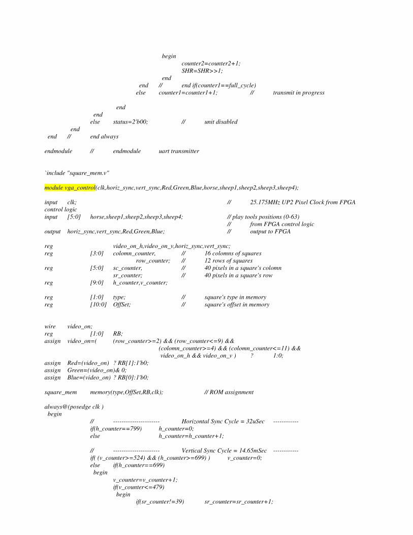
begin counter2=counter2+1; SHR=SHR>>1; end end // end if(counter1==full_cycle) else counter1=counter1+1; // transmit in progress end end else status=2'b00; // unit disabled end end // end always endmodule // endmodule uart transmitter include "square_mem.v"
module vga_control(clk,horiz_sync,vert_sync,Red,Green,Blue,horse,sheep1,sheep2,sheep3,sheep4); input clk; // 25.175MHz UP2 Pixel Clock from FPGA control logic input [5:0] horse,sheep1,sheep2,sheep3,sheep4; // play tools positions (0-63) // from FPGA control logic output horiz_sync,vert_sync,Red,Green,Blue; // output to FPGA reg video_on_h,video_on_v,horiz_sync,vert_sync; reg [3:0] colomn_counter, // 16 colomns of squares row_counter; // 12 rows of squares reg [5:0] sc_counter, // 40 pixels in a square's colomn sr_counter; // 40 pixels in a square's row reg [9:0] h_counter,v_counter; reg [1:0] type; // square's type in memory reg [10:0] OffSet; // square's offset in memory wire video_on; reg [1:0] RB; assign video_on=( (row_counter>=2) && (row_counter<=9) && (colomn_counter>=4) && (colomn_counter<=11) && video_on_h && video_on_v ) ? 1:0; assign Red=(video_on) ? RB[1]:1'b0; assign Green=(video_on)& 0; assign Blue=(video_on) ? RB[0]:1'b0; square_mem memory(type,OffSet,RB,clk); // ROM assignment always@(posedge clk ) begin // ---------------------- Horizontal Sync Cycle = 32uSec ------------ if(h_counter==799) h_counter=0; else h_counter=h_counter+1; // ---------------------- Vertical Sync Cycle = 14.65mSec ------------ if( (v_counter>=524) && (h_counter>=699) ) v_counter=0; else if(h_counter==699) begin v_counter=v_counter+1; if(v_counter<=479) begin if(sr_counter!=39) sr_counter=sr_counter+1;

else begin sr_counter=0; if(row_counter<11) row_counter=row_counter+1; else row_counter=0; end end else begin sr_counter=0; row_counter=0; end end // ---------------------- Horizontal Sync generation ------------ if( (h_counter<=755) && (h_counter>=659) ) horiz_sync=0; else horiz_sync=1; // ---------------------- Verticl Sync generation ------------ if( (v_counter<=494) && (v_counter>=493) ) vert_sync=0; else vert_sync=1; // ---------------------- RGB Generation ----------------------- if(h_counter<=639) // Horizontal timing begin video_on_h=1; if(sc_counter!=39) sc_counter=sc_counter+1; else begin sc_counter=0; if(colomn_counter<15) colomn_counter=colomn_counter+1; else colomn_counter=0; end end else video_on_h=0; if(v_counter<=479) video_on_v=1; // Vertical timing else video_on_v=0; // -------------------- RGB source from ROM generation (Type + OffSet) if( (video_on_h==1) && (video_on_v==1) ) if( (row_counter>=2) && (row_counter<=9) && (colomn_counter>=4) && (colomn_counter<=11) ) begin case( (row_counter-2)*8 + (colomn_counter-4) ) horse : type=3; sheep1: type=2; sheep2: type=2; sheep3: type=2; sheep4: type=2; default : begin if(colomn_counter[0] == row_counter[0]) type=0; else type=1; end endcase OffSet=sr_counter*40+sc_counter; end end // end always endmodule // endmodule vga_control

module square_mem(type,OffSet,q,inclock); input inclock; input [1:0] type; input [10:0] OffSet; output [1:0] q; wire [12:0] address; assign address=type*1600+OffSet; lpm_rom square_rom( .q(q), .address(address),.inclock(inclock)); defparam square_rom.LPM_WIDTH =2; defparam square_rom.LPM_WIDTHAD =13; defparam square_rom.LPM_FILE="square_mem.mif"; defparam square_rom.LPM_NUMWORDS =6400; //defparam square_rom.LPM_ADDRESS_CONTROL ="UNREGISTERED"; defparam square_rom.LPM_OUTDATA ="UNREGISTERED"; endmodule // endmodule square_mem

Appendix E
