failover control logic - … · 1.1.2.4 power supply voltage ... failover control logic basic block...
TRANSCRIPT

May, 1980 A-80-200-2379-1 WP0322A
WABCD ~~
SERVICE MANUAL 6129
FAILOVER CONTROL LOGIC
OPERATION INSTALLATION AND MAINTENANCE
UNION SWITCH & SIGNAL DIVISION AMERICAN STANDARD INC.
Swissvale, PA 15218
Section
I
II
III
IV
v
VI
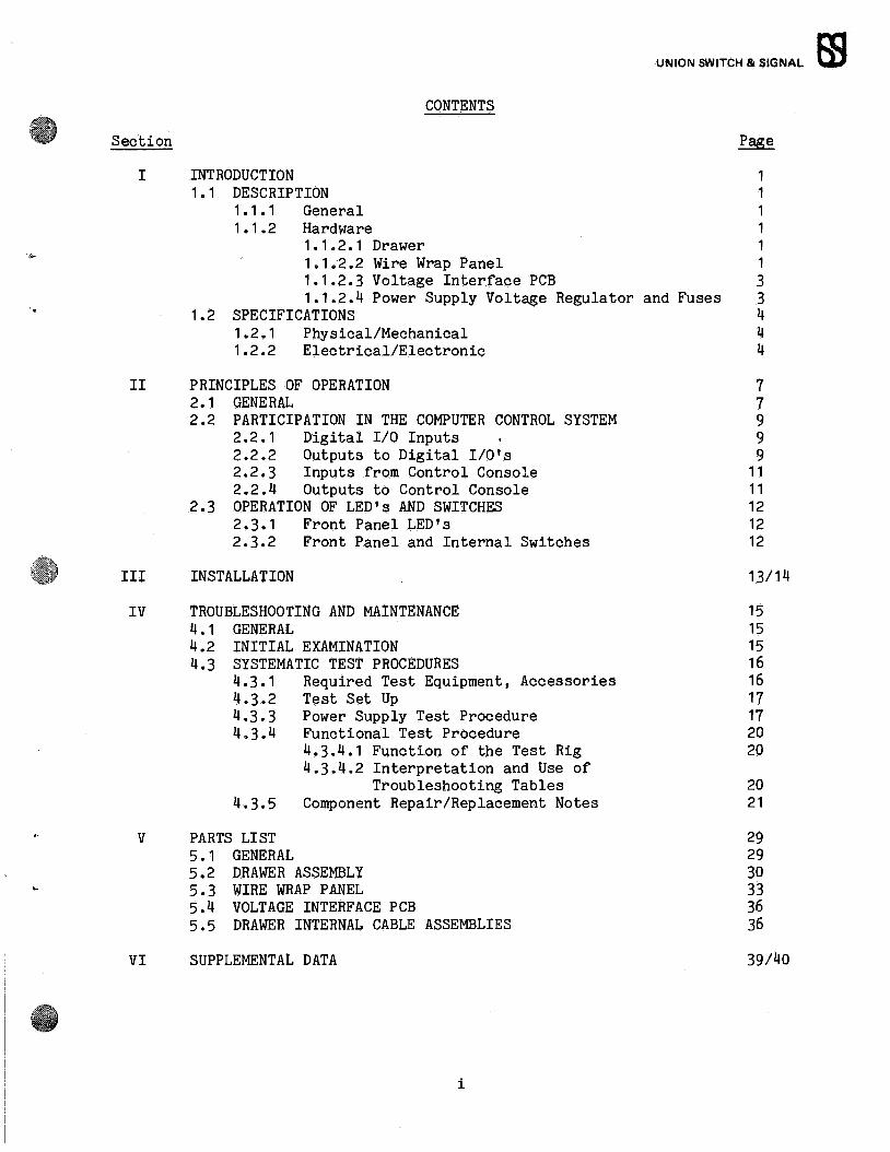
UNION SWITCH & SIGNAL m CONTENTS
INTRODUCTION 1.1 DESCRIPTION
1 • 1 • 1 General 1.1.2 Hardware
1.1.2.1 Drawer 1.1.2.2 Wire Wrap Panel 1.1.2.3 Voltage Interface PCB 1.1.2.4 Power Supply Voltage Regulator and Fuses
1.2 SPECIFICATIONS 1.2.1 Physical/Mechanical 1.2.2 Electrical/Electronic
PRINCIPLES OF OPERATION 2.1 GENERAL 2.2 PARTICIPATION IN THE COMPUTER CONTROL SYSTEM
2.2.1 Digital I/0 Inputs 2.2.2 Outputs to Digital I/O's 2.2.3 Inputs from Control Console 2.2.4 Outputs to Control Console
2.3 OPERATION OF LED's AND SWITCHES 2.3.1 Front Panel LED's 2.3.2 Front Panel and Internal Switches
INSTALLATION
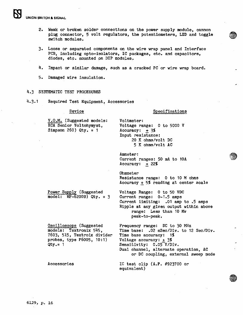
TROUBLESHOOTING AND MAINTENANCE 4.1 GENERAL 4.2 INITIAL EXAMINATION 4.3 SYSTEMATIC TEST PROCEDURES
4.3.1 Required Test Equipment, Accessories 4.3.2 Test Set Up 4.3.3 Power Supply Test Procedure 4.3.4 Functional Test Procedure
4.3.4.1 Function of the Test Rig 4.3.4.2 Interpretation and Use of
Troubleshooting Tables 4.3.5 Component Repair/Replacement Notes
PARTS LIST 5.1 GENERAL 5.2 DRAWER ASSEMBLY 5.3 WIRE WRAP PANEL 5.4 VOLTAGE INTERFACE PCB 5.5 DRAWER INTERNAL CABLE ASSEMBLIES
SUPPLEMENTAL DATA
i
1 1 1 1 1 1 3 3 4 4 4
7 7 9 9 9
11 11 12 12 12
13/14
15 15 15 16 16 17 17 20 20
20 21
29 29 30 33 36 36
39/40
m UNION SWITCH & SIGNAL
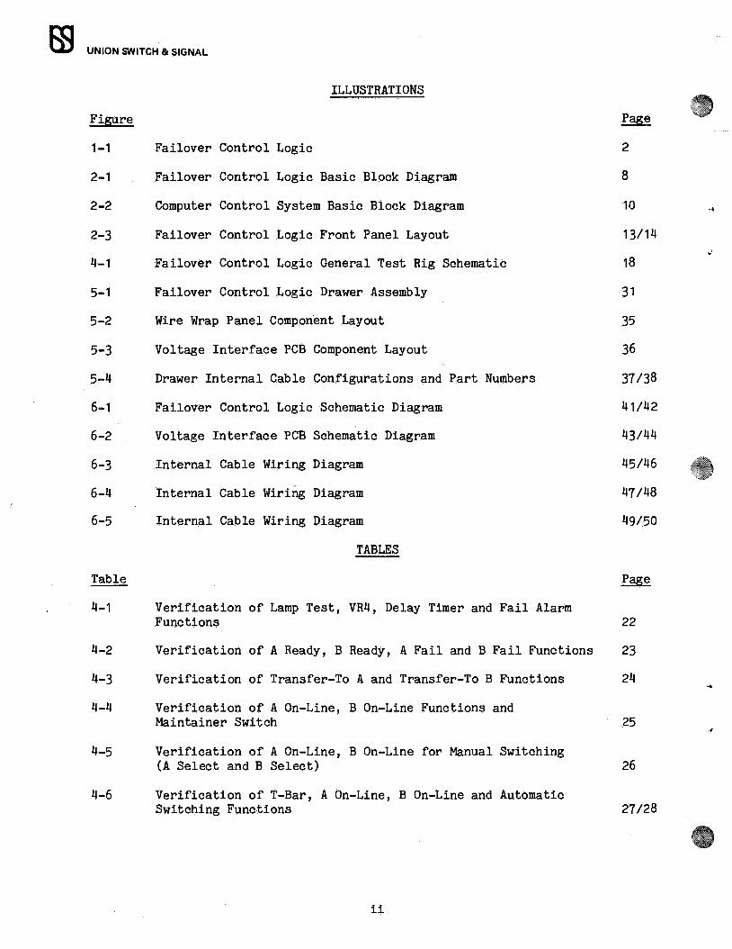
Figure
1-1
2-1
2-2
2-3
4-1
5-1
5-2
5-3
5-4
6-1
6-2
6-3
6-4
6-5
Table
4-1
4-2
4-3
4-4
4-5
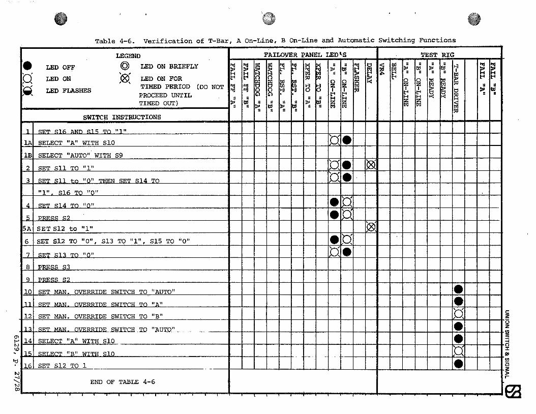
4-6
ILLUSTRATIONS
Failover Control Logic
Failover Control Logic Basic Block Diagram
Computer Control System Basic Block Diagram
Failover Control Logic Front Panel Layout
Failover Control Logic General Test Rig Schematic
Failover Control Logic Drawer Assembly
Wire Wrap Panel Component Layout
Voltage Interface PCB Component Layout
Drawer Internal Cable Configurations and Part Numbers
Failover Control Logic Schematic Diagram
Voltage Interface PCB Schematic Diagram
Internal Cable Wiring Diagram
Internal Cable Wiring Diagram
Internal Cable Wiring Diagram
TABLES
Verification of Lamp Test, VR4, Delay Timer and Fail Alarm Functions
Verification of A Ready, B Ready, A Fail and B Fail Functions
Verification of Transfer-To A and Transfer-To B Functions
Verification of A On-Line, B On-Line Functions and Maintainer Switch
Verification of A On-Line, B On-Line for Manual Switching (A Select and B Select)
Verification of T-Bar, A On-Line, B On-Line and Automatic Switching Functions
ii
2
8
10
13/14
18
31
35
36
37/38
41/42
43/44
45/46
47/48
49/50
22
23
24
25
26
27/28
1.1 DESCRIPTION
1 • 1 • 1 General
SECTION I INTRODUCTION
UNION SWITCH & SIGNAL ffi
The Failover Control Logic (Figure 1-1) is a solid-state device which manages the switching of control responsibilities between a main computer and a standby computer. The Failover monitors the Watchdog circuits of both computers for a failure indication, and provides warnings to the computer operator when a failure has occurred. The computers and the control console are tied together with the Failover such that all elements of the system are constantly updated as to (a) which computer is on-line, (b) which computer has failed, (c) whether the alternate computer is ready to go on-line, (d) when the alternate computer is ready to go on-line, (e) when the. switchover takes place and (f) when the alternate·computer goes on-line. Various switches on the Failover allow for fully automatic monitoring and switchovers, or manual switchovers when failures occur or for routine maintenance.
1.1.2 Hardware
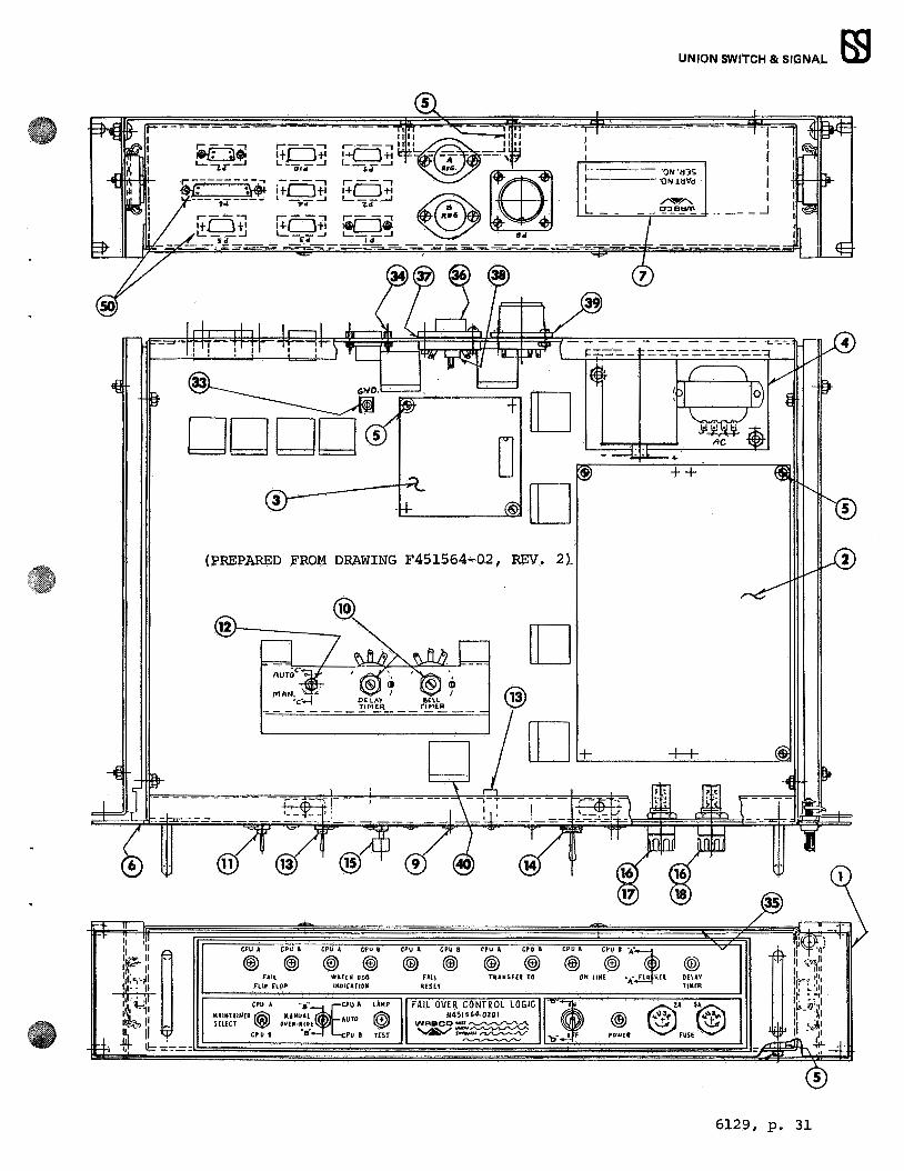
1.1.2.1 Drawer (N451564-0102)
The Failover Control Logic is packaged in a standard 19" equipment rack drawer which, in turn, is mounted on a sliding assembly for routine access. Subassemblies are bolted to the base and side panels. These assemblies include (Figure 5-1) the Failover Logic Wire Wrap Panel, a power supply, the Voltage Interface PCB, 2 IC voltage regulators, 20 LED indicators, 2 fuses, 4 toggle control switches, 3 fuses, 10 external connector plugs and 5 internal ribbon cable assemblies. A central mounting bracket is also attached to the drawer base; it contains the auto/manual mode selection switch and two 1-megaohm potentiometers (DELAY TIMER and BELL TIMER).
The voltage regulators and external cable connectors are attached to the back panel of the unit. The connectors include 9 industry standard "D" multi-pin (9 or 25 contacts) for external computer equipment and a cannon plug connector for application of operating power. Wiring between the various assemblies in the drawer consists of color-coded, prefabricated ribbon cables which are equipped with DIP sockets and/or the "D" connector plugs, discreet leads and some spares. (Refer to Figure 5-4 for complete configuration.)
1.1.2.2 Wire Wrap Panel (N451412-0501, Figure 5-2)
The Wire Wrap Panel contains the components which control the monitoring and switching functions of the Failover. The assembly consists of a raised fiberglas epoxy board containing 60, 16-pin dual in-line package (DIP) sockets. Each socket receptacle has a corresponding terminal pin on the opposite side of the panel; electrical connections between these DIP pins is accomplished with discreet insulated wiring, rather than PCB copper tracks.
The Wire Wrap Panel mounts a variety of plug-in relays, integrated circuits and support components in two groups designated "A" and "B". The "A" and "B" designations are only given for component location purposes and do not relate to the operation of the Failover.
6129, p. 1

ffi UNION SWITCH & SIGNAL
...
Figure 1-1. Failover Control Logic
6129, p. 2
UNION SWITCH & SIGNAL
Seven electro-optical couplers are provided for electrical isolation of the Failover decision-making logic components from TTL input signals. Ten reed relays serve as output ports for indications sent to the computer system control console; the relays act as buffers or isolation devices against any transients in the console power supply. Twenty-one positive digital logic ICs (including various gates and a timing circuit) comprise the decision-making components of the system. Reverse-polarity diodes are installed on one package to protect 5 volt component power sources entering the wire wrap panel. Capacitors are also installed at this and other panel locations to filter transients and line noise. Resistors are incorporated on the panel via several varieties of resistors networks (resnets); each network is mounted on its own DIP socket.
External connections to the Wire Wrap Panel are made on 16-pin DIP's sharing one column of panel sockets and two sockets of an adjacent column. The female connector pins designated J1 and J2 at one end and several DIP sockets are not used in the present Failover configuration. For a complete schematic representation of the Wire Wrap Panel, refer to Figure 6-2. (The schematic shows a "stop hump" input. This is included for special classification yard applications. For information on other possible applications of this input, consult US&S Systems Marketing and Engineering.)
1.1.2.3 Voltage Interface PCB (N451422-4301, Figure 5-3)
The Interface PCB is designed to interface commercial VAC power with the Failover power supply converter, then interface regulated power with the control components on the Wire Wrap Panel. This assembly is a raised fiberglas epoxy board which incorporates PCB copper tracks, faston connectors and voltage regulating components. The principal component of the PCB is a metal-oxide varistor (MOV) which suppresses AC line transient voltages which could otherwise damage the power supply. Two 10 MFD and two .001 MFD electolytic capacitors are used for decoupling of the 5 VDC voltage regulators (see Section 1.1.2.4 following). A diode is also present for reverse polarity protection. The Voltage Interface PCB also contains one set of test points for measurement of the 5 VDC voltage sources and another set to measure the 12 VDC, unregulated source. A single ribbon wire connector is installed on the PCB to supply regulated power to the IC's etc. on the Wire Wrap Panel.
1.1.2.4 Power Supply, Voltage Regulators and Fuses
The power supply module in the corner of the drawer contains a transformer coil and an electrolytic capacitor. The power supply's function is to convert 117 VAC, 60 Hz commercial power into unregulated 12 VDC, at up to 1.2 amps. This voltage is then translated into 5 VDC by the two voltage regulator components on the back panel. These components absorb unregulated supply voltage up to 30 VDC before automatically opening; the output holds at 5 VDC, with foldback current limiting at 3 amps. The 5 VDC regulators provide current acceptable to the Failover Logic components. The "A" regulator supplies the relays and "B" the TTL components (these designations are not related to the A and B divisions of the Wire Wrap Panel).
The power supply module is also equipped with a 2 amp fuse which is installed in series with the 2 amp fuse on the front panel of the drawer. The 5 amp fuse, also on the front panel, provides protection on the 24 volt lamp circuit
6129, p. 3
UNION SWITCH & SIGNAL
coming from the CPU control panel to the CPU A and Bon-line circuits (refer to Figure 6-1). For complete electrical specifications of the power supply and other components, refer to Section 1.2 following.
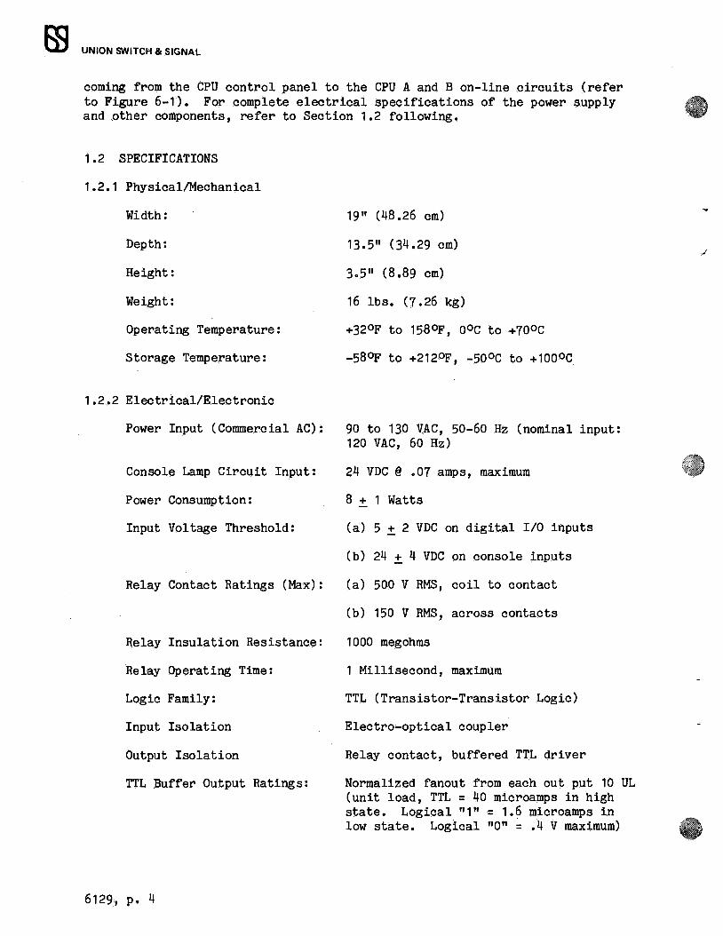
1.2 SPECIFICATIONS
1.2.1 Physical/Mechanical
Width:
Depth:
Height:
Weight:
Operating Temperature:
Storage Temperature:
1.2.2 Electrical/Electronic
Power Input (Commercial AC):
Console Lamp Circuit Input:
Power Consumption:
Input Voltage Threshold:
Relay Contact Ratings (Max):
Relay Insulation Resistance:
Relay Operating Time:
Logic Family:
Input Isolation
Output Isolation
TTL auffer Output Ratings:
6129, p. 4
19 11 (48.26 cm)
13 • 5" ( 34 • 29 cm)
3.5" (8.89 cm)
16 lbs. (7 .26 kg)
+32°F to 1580F, ooc to +7ooc
-580F to +212oF, -500C to +1000C
90 to 130 VAC, 50-60 Hz (nominal input: 120 VAC, 60 Hz)
24 VDC@ .07 amps, maximum
8 ± 1 Watts
(a) 5 ± 2 VDC on digital I/0 inputs
(b) 24 + 4 VDC on console inputs
(a) 500 V RMS, coil to contact
(b) 150 V RMS, across contacts
1000 megohms
1 Millisecond, maximum
TTL (Transistor-Transistor Logic)
Electro-optical coupler
Relay contact, buffered TTL driver
Normalized fanout from each out put 10 UL (unit load, TTL= 40 microamps in high state. Logical "1" = 1.6 microamps in low state. Logical "0" = .4 V maximum)
...
UNION SWITCH & SIGNAL
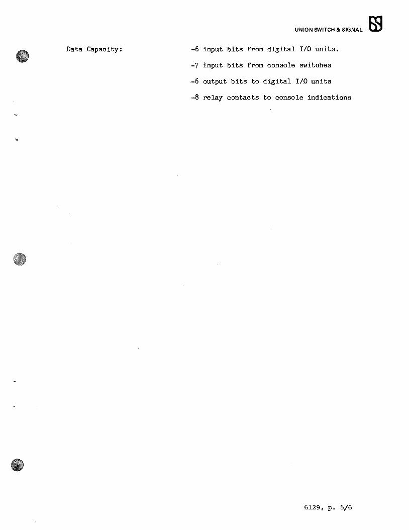
Data Capacity: -6 input bits from digital I/0 units.
-7 input bits from console switches
-6 output bits to digital I/0 units
-8 relay contacts to console indications
6129, p. 5/6

2.1 GENERAL
SECTION II PRINCIPLES OF OPERATION
UNION SWITCH & SIGNAL m
The Failover Control Logic is used with a main or "hot" computer and a standby computer, each having a digital input/output (I/0) unit capable of monitoring the status of the other computer; the computers use special software which manage transfers when failures occur. The Failover operates in three possible modes: Automatic, Manual or Override.
In the event of a failure of the on-line CPU, the Failover can be programmed to transmit automatic switching commands to transfer controls from the failed CPU to the standby CPU. The Failover contains decision-making logic which determines if the standby is capable of assuming on-line responsibilities. Should the standby fail, the Failover will transfer control back to the main CPU, provided the original fault has been elevated and computer reset functions enabled.
These operations can also be accomplished manually on the Failover. When the system is placed in the manual mode and a switchover is later required, an indicator tells the operator to carry out the actual transfer. A switch within the drawer assembly programs the Failover for manual or automatic operation. One or the other mode is selected according to external system requirements and application.
A manual override switch on the Failover allows direct switching between the CPU's should the Failover itself develop a fault. The Failover can also provide manual switchover of CPU's when the CPU's are working properly. This is accomplished with a maintainer switch on the front of the unit and is done for routine maintenance purposes.
As shown in Figure 2-1, the Failover Control Logic accepts TTL level inputs from both CPU's and contact-sense inputs from the control console. The basic function of the TTL inputs is to inform the Failover (and, through the Failover, the other elements of the system) when a given computer has made or is about to make some kind of operational change. The basic function of the console inputs is to allow the operator to manually transfer control (Failover in the manual mode) from one CPU to the other and then cancel failure indications fom either CPU. (Functioning of the Failover within the computer control system as a whole is discussed further in Section 2.2).
All Failover inputs are aligned and conducted through the optical couplers to TTL buffers which, in turn, drive certain Failover LED's, the decision-making logic and a timing circuit. The timing circuit is included to pace the actions of the logic with those of the computers and control equipment in the system.
The decision-making logic provides outputs to the CPU digital I/O's through a separate array of buffer/drivers. The basic function of these outputs is to relay the CPU failure and on-line indications from the Failover to both CPU digital I/O's. A separate TTL output from the decision-making logic goes to the transfer or T-Bar module (relay equipment which executes the transfer of controls from one CPU to the other) and represents the switching signals the Failover sends after all failure and ready indications have been processed.
6129, p. 7

O'I I-'
"' \0 ... tc, . (X)
LAMP TEST
CPU "A" INPUTS
(TTL)
CPU "B" INPUTS (TTL)
CONSOLE INPUTS
(CONTACT SENSE)
_,..
120VAC -+
-·-·-
FAILOVER LOGIC LOCAL INDICATIONS (L. E. D.'S, -
L. E. 0. DRIVERS (7404) ~
ELECTRO· OPTICAL
-
ISOLATOR . TTL.
DECISION BUFFERS
MAKING LOGIC
TTL ELECTRO· BUFFERS OPTICAL -
ISOLATOR
r t ELECTRO· CIRCUIT LOCAL OPTICAL TIMING SWITCH
ISOLATOR CONTROL
REG 5V.D.C.
POWER - TO ALL INTERNAL SUPPLY CIRCUIT REQUIREMENTS
Figure 2-1. Failover Control Logic Basic Block Diagram
CPU "A" OUTPUTS
(TTL.}
CPU "B" OUTPUTS
(TTL.)
I _ "T"BAR DRIVER •
CONSOLE - INDICATION
(RELAY CONTACT)
~
EE c z 0 z i ~ :t: ~ Cl)
i5 z )> r
UNION SWITCH & SIGNAL
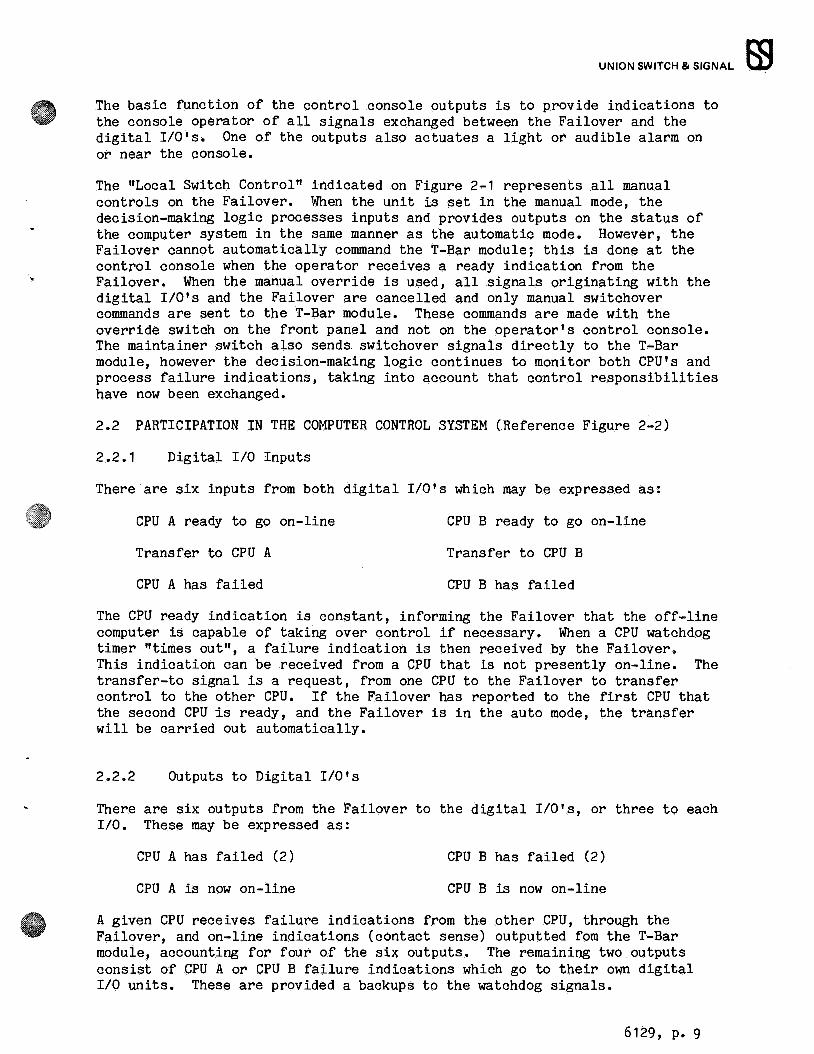
The basic function of the control console outputs is to provide indications to the console operator of all signals exchanged between the Failover and the digital I/O's. One of the outputs also actuates a light or audible alarm on or near the console.
The "Local Switch Control" indicated on Figure 2-1 represents all manual controls on the Failover. When the unit is set in the manual mode, the decision-making logic processes inputs and provides outputs on the status of the computer system in the same manner as the automatic mode. However, the Failover cannot automatically command the T-Bar module; this is done at the control console when the operator receives a ready indication from the Failover. When the manual override is used, all signals originating with the digital I/O's and the Failover are cancelled and only manual switchover commands are sent to the T-Bar module. These commands are made with the override switch on the front panel and not on the operator's control console. The maintainer switch also sends switchover signals directly to the T-Bar module, however the decision-making logic continues to monitor both CPU's and process failure indications, taking into account that control responsibilities have now been exchanged.
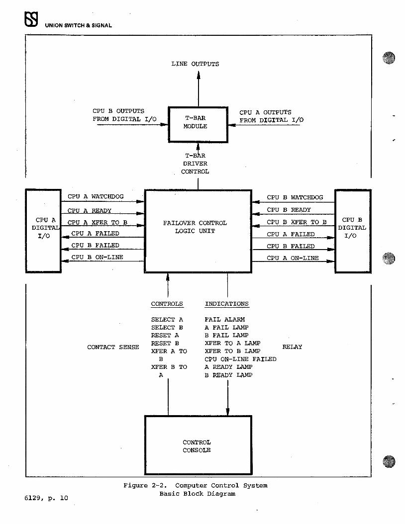
2.2 PARTICIPATION IN THE COMPUTER CONTROL SYSTEM (Reference Figure 2-2)
2.2.1 Digital I/0 Inputs
There are six inputs from both digital I/O's which may be expressed as:
CPU A ready to go on-line CPU Bready to go on-line
Transfer to CPU A Transfer to CPU B
CPU A has failed CPU B has failed
The CPU ready indication is constant, informing the Failover that the off-line computer is capable of taking over control if necessary. When a CPU watchdog timer "times out", a failure indication is then received by the Failover. This indication can be received from a CPU that ls not presently on-line. The transfer-to signal is a request, from one CPU to the Failover to transfer control to the other CPU. If the Failover has reported to the first CPU that the second CPU is ready, and the Failover is in the auto mode, the transfer will be carried out automatically.
2.2.2 Outputs to Digital I/O's
There are six outputs from the Failover to the digital I/O's, or three to each I/0. These may be expressed as:
CPU A has failed (2) CPU B has failed (2)
CPU A is now on-line CPU Bis now on-line
A given CPU receives failure indications from the other CPU, through the Failover, and on-line indications (contact sense) outputted fom the T-Bar moduie, accounting for four of the six outputs. The remaining two outputs consist of CPU A or CPU B failure indications which go to their own digital I/0 units. These are provided a backups to the watchdog signals.
6129, p. 9
ffi UNION SWITCH & SIGNAL
LINE OUTPUTS
CPU B OUTPUTS CPU A OUTPUTS FROM DIGITAL I/0 T-BAR FROM DIGITAL I/0
CPU A WATCHDOG
CPU A READY
CPU A CPU A XFER TO B DIGITAL1-~.:::.....;~::::.:::.:.:.-=-:::.....:::..-...,~ I/O CPU A FAILED
CPU B FAILED
CPU BON-LINE
CONTACT SENSE
- MODULE -
T-Bl DRIVER
CONTROL
CPU B WATCHDOG
CPU BREADY
FAILOVER CONTROL LOGIC UNIT
CPU B XFER TO B CPU B .... 1-...::.::...:;_.;:;_;:;;;;;...:;;;.;;;,.;_;;;_.;;...;;;_~DIGITAL CPU A FAILED I/0
CPU B FAILED
CPU A ON-LINE
CONTROLS INDICATIONS
SELECT A FAIL ALARM SELECT B A FAIL LAMP RESET A B FAIL LAMP RESET B XFER TO A LAMP RELAY XFER A TO XFER TO B LAMP
B CPU ON-LINE FAILED XFER B
A TO A READY LAMP
BREADY LAMP
CONTROL CONSOLE
6129, p. 10
Figure 2-2. Computer Control System Basic Block Diagram
UNION SWITCH & SIGNAL
2.2.3 Inputs From Control Console
There are six possible inputs from the computer system control console to the Failover. These may be expressed as:
Place CPU A on-line Place CPU Bon-line
Transfer control from CPU B to CPU A Transfer control from CPU A to CPU B
Remove CPU B fail indication Remove CPU A fail indication
,.., Either CPU may be placed on-line manually from the control console, or from a field location through the control console. These indications are sent through the maintainer switch circuit on the Failover and execute the same kind of control changes as the maintainer switch.
The transfer-to input is sent manually only when the Failover is in the manual mode. This input will not result in a transfer unless the Failover observes that the alterntate CPU is ready to go on-line. The presently on-line CPU must also show a watchdog failure indication.
The operator removes the CPU fail indication from both digital I/0 units via inputs to the Failover. The manual reset is required whether or not the Failover is in the manual mode, and is done after the computer problem has been corrected. A-Fail Reset represents removal of the A-fail indication; B-Fail Reset represents removal of the B-fail indication.
2.2.4 Outputs to Control Console
There are eight possible outputs from the Failover to the computer system control console. These may be expressed as:
Indicate that A has failed
Indicate that control is transferring to A
Indicate that A is ready to go on-line
Trip fail alarm
Indicate that B has failed
Indicate that control is transferring to B
Indicate that Bis ready to go on-line
Indicate that on-line CPU has failed
The status indications from the failover to the control console allow the operator to coordinate actions from the control room. Should a failure occur in the on-line computer, the failover will trigger a visible or audible alarm to attract the attention of the operator. Only a visible indicator will show that the failure has occurred with the backup and not the on-line machine.
The Failover will provide ready and transfer-to indications in both the automatic and manual modes.
6129, p. 11
UNION SWITCH & SIGNAL
2.3 OPERATION OF LED'S AND SWITCHES
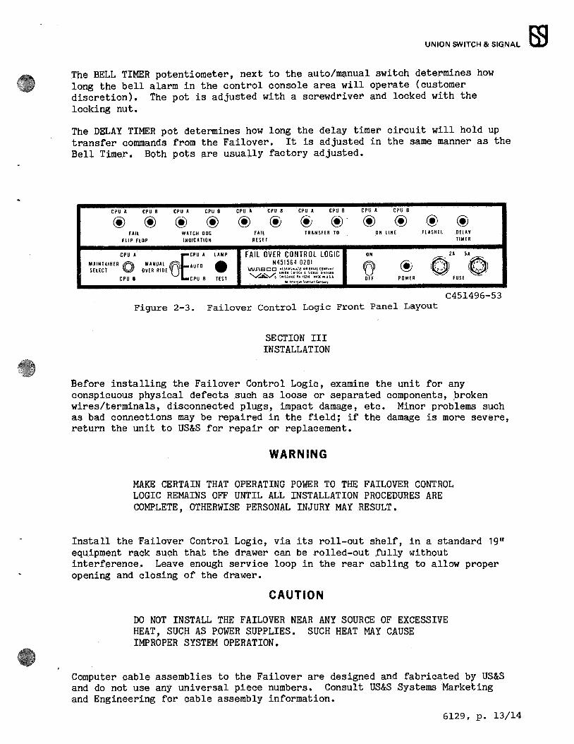
2.3.1 Front Panel LED's (Reference Figure 2-3)
The FAIL FLIP FLOP LED's indicate when the Failover has translated a CPU watchdog fail signal into fail outputs to both digital I/0 units (flip-flop trigger circuits are used for this purpose). When a fail reset signal is received from the control console, the circuit goes back to the original "not failed" indication and the corresponding LED goes out.
The WATCHDOG INDICATION LED's monitor the individual watchdog timer inputs from the CPU's. When a watchdog is reset on its CPU, the corresponding Failover LED goes out.
The FAIL RESET LED's operate in conjunction with the cancelling of the fail flip flop circuits. The associated LED lights only as long as the reset signal is present in the Failover·.
The TRANSFER-TO LED's report when a CPU has issued a request for control to be switched over to the alternate CPU. In the manual mode, a given LED will flash to indicate that computer control is ready to be transferred. In the automatic mode, one of these LED's will flash only very briefly as the request is issued and then immediately carried out.
The On-LINE LED's indicate which CPU is presently on-line. One of these LED's will remain on through a failure sequence until the T-Bar module switches control to the other CPU; then the other LED lights.
The FLASHER LED indicates when the Failover flasher timer is operating and is used for diagonostic purposes.
The DELAY TIMER LED lights when the delay timer in the Failover is actuated. The duration of the delay and LED indication is determined by the DELAY TIMER potentiometer setting (see Section 2.3.2 following).
The POWER LED lights when AC power is applied to the Failover (via the ON switch).
2.3.2 Front Panel and Internal Switches
The MAINTAINER SELECT switch (transfers control from one CPU to the other) is designed not to lock control responsibilities on one or the other CPU (toggle returns to center position) as occurs with the Manual Override.
The MANUAL OVERRIDE switch does lock on one CPU or the other so that all CPU and Failover indications are cut off until the operator returns the system to Auto. This Auto represents normal operation of the Failover in either the Auto or Manual modes.
The LAMP TEST pushbutton applies power from one of the 5 volt regulators simultaneously to all front panel LED's; this is done to determine if the LED's themselves are operating properly.
The ON switch applies the commercial AC power to the Failover.
6129, p. 12
UNION SWITCH & SIGNAL
The BELL TIMER potentiometer, next to the auto/manual switch determines how long the bell alarm in the control console area will operate (customer discretion). The pot is adjusted with a screwdriver and locked with the locking nut.
The DELAY TIMER pot determines how long the delay timer circuit will hold up transfer commands from the Failover. It is adjusted in the same manner as the Bell Timer. Both pots are usually factory adjusted.
CPU A CPU 8 CPU A CPU B CPU A CPU 8 CPU A CPU 8 CPU A CPU B
@ @ @ @ @ @ @ @ @ @ ~I @ fAIL WATCH DOG FAIL TRANSFER TO ON llNE FLASH[!. DELAY
FLIP FLOP INOICA TION RESET TIMER
CPU A LAMP FAIL OVER CONTROL LOGIC ON 2A SA
ECPU A MAINTAINER O MANUAL fj AUTO • N451564 ·0201 {J @ 10 i©) SELECT OVER RIDE WABCO flfl'>ll•i. .. ,,,,'.( Alt !~Ul COUl'Olf ,1~r ~,,
"-"'A.~, ~::~:,~~'~i",:2,;1'~!~0~1i1:: CPU 8 CPU 8 !EST .,.,,....0:..,.,,-. ... tc~"'' Off POWER FUSE
C451496-53 Figure 2-3. Failover Control Logic Front Panel Layout
SECTION III INSTALLATION
Before installing the Failover Control Logic, examine the unit for any conspicuous physical defects such as loose or separated components, proken wires/terminals, disconnected plugs, impact damage, etc. Minor problems such as bad connections may be repaired in the field; if the damage is more severe, return the unit to US&S for repair or replacement.
WARNING
MAKE CERTAIN THAT OPERATING POWER TO THE FAILOVER CONTROL LOGIC REMAINS OFF UNTIL ALL INSTALLATION PROCEDURES ARE COMPLETE, OTHERWISE PERSONAL INJURY MAY RESULT.
Install the Failover Control Logic, via its roll-out shelf, in a standard 19" equipment rack such that the drawer can be rolled-out fully without interference. Leave enough service loop in the rear cabling to allow proper opening and closing of the drawer.
CAUTION
DO NOT INSTALL THE FAILOVER NEAR ANY SOURCE OF EXCESSIVE HEAT, SUCH AS POWER SUPPLIES. SUCH HEAT MAY CAUSE IMPROPER SYSTEM OPERATION.
Computer cable assemblies to the Failover are designed and fabricated by US&S and do not use any universal piece numbers. Consult US&S Systems Marketing and Engineering for cable assembly information.
6129, p. 13/14
UNION SWITCH & SIGNAL m
4.1 GENERAL
SECTION IV TROUBLESHOOTING AND MAINTENANCE
The troubleshooting and maintenance steps given in this section should only be employed by shops with the proper test equipment and personnel qualified to perform such work. If the Failover Control Logic is not repairable in the field, US&S should be contacted for repair or replacement of the faulty unit, either through the nearest district sales representative or through the Sales Manager at:
Union Switch & Signal Division American Standard Inc. 1789 South Braddock Avenue Swissvale, PA. 15218
Attn: Customer Service Department
Telephone: 412/273-4000 TWX: 710-664-2096 Telex 86-6448
Troubleshooting procedures in this section include performance checks on the power supply components and operational tests of the Failover monitoring and processing circuits. The circuit tests only narrow the source of the problem to functional areas such as A Ready, B Ready, A Fail, B Fail, etc. The maintainer must then carry out standard component and circuit continuity tests to pinpoint the source of the problem. Procedures for these types of tests are not given in this manual. Use the Failover Control Logic schematic diagrams (Figure 6-1 and 6-2) for in-depth component troubleshooting.
CAUTION
WHEN TESTING FAILOVER CONTROL LOGIC SOLID-STATE COMPONENTS, MAKE CERTAIN TO OBSERVE PROPER OPERATING VOLTAGE AND POLARITIES, OTHERWISE THESE COMPONENTS MAY BE DAMAGED WHEN TEST POWER IS APPLIED. ALSO, MAKE CERTAIN TO OBSERVE CORRECT POLARITIES WHEN INSTALLING A NEW COMPONENT OR REINSTALLING AN EXISTING COMPONENT, OTHERWISE THESE MAY BE DAMAGED WHEN FAILOVER OPERATING POWER IS APPLIED.
4.2 INITIAL EXAMINATION
WARNING
MAKE CERTAIN THAT OPERATING POWER TO THE FAILOVER IS TURNED OFF, BEFORE ANY "HANDS ON" MAINTENANCE IS PERFORMED, OTHERWISE PERSONAL INJURY MAY RESULT.
A fault in the Failover Control Logic unit may be traced to an outward physical defect. Before conducting operational tests, check the Failover for:
1. Loose or separated wire/cable connector, including ribbon DIP connector sockets on the Wire Wrap Panel and Fastons attached to the Interface PCB.
6129, p. 15
UNION SWITCH & SIGNAL
2. Weak or broken solder connections on the power supply module, cannon plug connector, 5 volt regulators, the potentiometers, LED and toggle switch modules.
3. Loose or separated components on the wire wrap panel and Interface PCB, including opto-isolators, IC packages, etc. and capacitors, diodes, etc. mounted on DIP modules.
4. Impact or similar damage, such as a cracked PC or wire wrap board.
5. Damaged wire insulation.
4.3 SYSTEMATIC TEST PROCEDURES
4.3.1 Required Test Equipment, Accessories
Device
v.o.M. (Suggested models: RCA Senior Voltohymyst, Simpson 260) Qty.= 1
Power Suppl! (Suggested model: HP-62008) Qty.= 3
Oscilloscope (Suggested models: Textronix 545, 7603, 515, Textroix divider probes, type P6005, 10:1) Qty.= 1
Accessories
6129, p. 16
Specifications
Voltmeter: Voltage range: Oto 5000 V Accuracy : + 3% Input resistance:
20 K ohms/volt DC 5 K ohms/volt AC
Ammeter: Current ranges: 50 mA to 10A Accuracy: + 22%
Ohmmeter Resistance range: 0 to 10 M ohms Accuracy.:!:. 5% reading at center scale
Voltage Range: 0 to 50 VDC Current range: 0-1.5 amps Current limiting: .01 amp to .5 amps Ripple at any given output within above
range: Less than 10 Mv peak-to-peak.
Frequency range: DC to 30 MHz Time base: .02 mSec/Div. to 12 Sec/Div. Time base accuracy: 1% Voltage accuracy:+ 3% Sensitivity: 0.05-V/Div. Dual channel, alternate operation, AC
or DC coupling, external sweep mode
IC test clip (A.P. #923700 or equivalent)

UNION SWITCH & SIGNAL ffi 4.3.2 Test Set Up
To conduct power supply and functional tests of the Failover, a special test rig must be assembled; this rig is shown schematically in Figure 4-1. The following items are required to assemble this rig:
Qty.
9
9
7
6
1
6
35
Item
1.6K ohm, 1/2 watt, 5% tolerance carbon resistors
Light Emitting Diodes
SPST pushbutton switches
SPST toggle switches
25-pin "D" connector plug, crimp wire contact
9-pin "D" connector plug, crimp wire contact
Connector pins for #24-20 AWG
1 Component breadboard
US&S Part Number
J721254*
J726150-0062**
J705727-0106*
J725468*
J709146-0101
J709146-0099
J703211-0012*
* Matching components from sources other than US&S may be used. ** HP5082-4415 LED recommended.
4.3.3 Power Supply Test Procedure
Before conducting this test procedure, check the continuity of the 2. amp fuse mounted on the power supply module. The complete test rig shown in Figure 4-1 is not connected up until Step 21 of the following procedure. Only the 24 VDC power supply is operated continuously in Steps 1 through 20, in conjunction with the V.O.M. and oscilloscope. The following steps must be carried out in the indicated order; do not begin at an intermediate step.
Operation
1. Turn on and adjust power supply to 24 VDC.
2. Turn off power supply.
3. Disconnect ribbon cable connector PL1 from the regulator PCB (N451522-4301) in the drawer.
Verification
1. 24 VDC + .5 VDC
6129, p. 17

m UNION SWITCH & SIGNAL
XFER TO B
READY
A WATCHDOG
,.;:i;.. STOP HUMP
S8 ,..:C.... FIELD B O.L.* ..;r::,_ S7 FIELD A O.L.*
S6 ,::C.... FIELD B SELECT
,..:C.... SS FIELD A SELECT _!...::c....
3 ;:c..-
B F.R.I.**
A F.R.I.**
B
A READY
BREADY
FAIL-BELL
VR-4
T-BAR DRIVE
*oN-LINE ** FAIL RESET INPUT
R
PL UG-PIN NO. P2-3
P2-8
Pl-3
Pl-8
P2-2
P2-7
Pl-2
Pl-7
Pl0-1
Pl0-6
P9-l
P9-6
P6-20
P6-7
P6-19
P6-6
P6-18
P6-5
P6-17
P6-21
P6-9
P6-22
P6-10
P6-23
P6-ll
P6-25
P7-l
PS-1
P6-l
l. ....................... __ Figure 4-1.
6129, p. 18
r-1
LO Pi
0 e
G
0 .....,,
0
~ • CJ U)
0 E-1
E-1 0 5
r-1 Pi
I.O f:Q .,x: I I I I (' I.O co Pi Pi Pi Pi
co Pi
~ Pi
-.:JI r-1
e a e
• • • • • • • • • • • • • •
e
0
(!) I
Pi
+
I LO
e
e 0
(:)
0 e
G 0
°' Pi
• • 0 0
0
G 0
24 VDC POWER SUPPLY
'c F 'lover Control Logi ai . General Test Rig
0 0 0 0 0 0
0 © 0
. !°'I O U)
0 ~
0 I.O
i 0 ~ ~ ~ .'O
@O
I I I 0 @ 0
~I@ 0 . z .
H..:l
~ ffi
CJ CJ
~ !;: O O N N rt, r-1 r-1 v
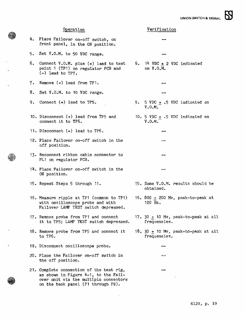
Operation
4. Place Failover on-off switch, on front panel, in the ON position.
5. Set V.O.M. to 50 VDC range.
6. Connect V.O.M. plus(+) lead to test point 1 (TP1) on regulator PCB and (-) lead to TP7.
7. Remove(+) lead from TP1.
8. Set V.O.M. to 10 VDC range.
9. Connect(+) lead to TP5.
10. Disconnect(+) lead from TP5 and connect it to TP6.
11. Disconnect(+) lead to TP6.
12. Place Failover on-off switch in the off position.
13. Reconnect ribbon cable connector to PL1 on regulator PCB.
14. Place Failover on-off switch in the ON position.
15. Repeat Steps 5 through 11.
16. Measure ripple at TP1 (common to TP1) with oscilloscope probe and with Failover LAMP TEST switch depressed.
17. Remove probe from TP1 and connect it to TP5; LAMP TEST switch depressed.
18. Remove probe from TP5 and connect it to TP6.
19. Disconnect oscilloscope probe.
20. Place the Failover on-off switch in the off position.
21. Complete connection of the test rig, as shown in Figure 4-1, to the Failover unit via the multipin connectors on the back panel (P1 through P9).
UNION SWITCH & SIGNAL m Verification
6. 14 VDC + 2 VDC indicated on V.O.M.
9. 5 VDC + .5 VDC indicated on v.o.M.
10. 5 VDC + .5 voe indicated on v.o.M.
15. Same V.O.M. results should be obtained.
16. Boo+ 200 Mv, peak-to-peak at 120 Hz.
17. 30 ± 10 Mv, peak-to-peak at all frequencies.
18. 30 ± 10 Mv, peak-to-peak at all frequencie'3.
6129, p. 19
UNION SWITCH & SIGNAL
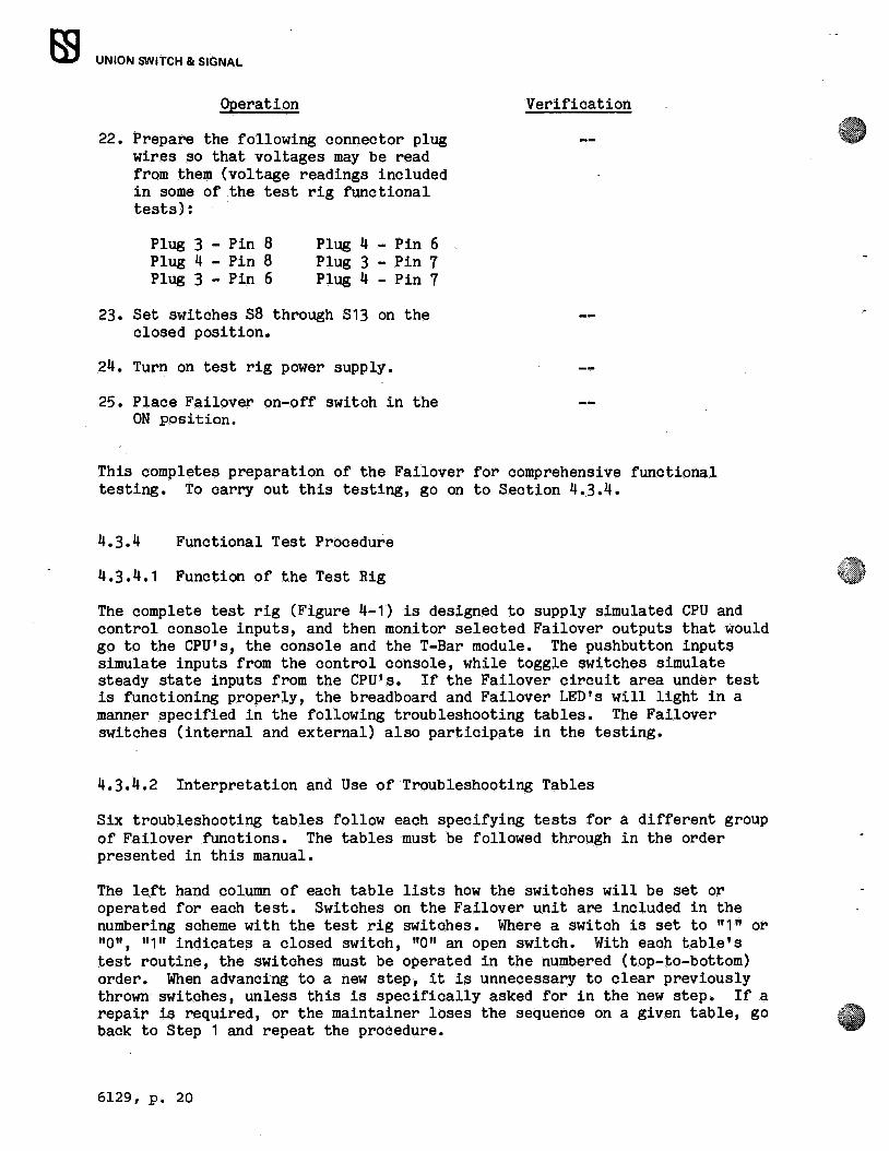
Operation
22. Prepare the following connector plug wires so that voltages may be read from them (voltage readings included in some of the test rig functional tests):
Plug 3 - Pin 8 Plug 4 - Pin 8 Plug 3 - Pin 6
Plug 4 - Pin 6 Plug 3 - Pin 7 Plug 4 - Pin 7
23. Set switches S8 through S13 on the closed position.
24. Turn on test rig power supply.
25. Place Failover on-off switch in the ON position.
Verification
This completes preparation of the Failover for comprehensive functional testing. To carry out this testing, go on to Section 4.3.4.
4.3.4 Functional Test Procedure
4.3.4.1 Function of the Test Rig
The complete test rig (Figure 4-1) is designed to supply simulated CPU and control console inputs, and then monitor selected Failover outputs that would go to the CPU's, the console and the T-Bar module. The pushbutton inputs simulate inputs from the control console, while toggle switches simulate steady state inputs from the CPU's. If the Failover circuit area under test is functioning properly, the breadboard and Failover LED's will light in a manner specified in the following troubleshooting tables. The Failover switches (internal and external) also participate in the testing.
4.3.4.2 Interpretation and Use of Troubleshooting Tables
Six troubleshooting tables follow each specifying tests for a different group of Failover functions. The tables must be followed through in the order presented in this manual.
The left hand column of each table lists how the switches will be set or operated for each test. Switches on the Failover unit are included in the numbering scheme with the test rig switches. Where a switch is set to "1" or 11011 , "1" indicates a closed switch, 11011 an open switch. With each table's test routine, the switches must be operated in the numbered (top-to-bottom) order. When advancing to a new step, it is unnecessary to clear previously thrown switches, unless this is specifically asked for in the new step. If a repair is required, or the maintainer loses the sequence on a given table, go back to Step 1 and repeat the procedure.
6129, p. 20
UNION SWITCH & SIGNAL
The middle columns indicate how the Failover front panel LED's should respond when the test switches are operated. The maintainer should be familiar with the operation of these LED's when the Failover is in normal service.
The right hand columns provide test rig LED responses to the switch operations and, on a limited number of tests, high/low voltage state readings taken on the Failover CPU fail and on-line outputs.
Using Step 3 of Table 1 as a sample procedure: The maintainer would press pushbutton S3 on the test rig. This simulates a B Fail Reset input from the control console. If the respective Failover circuit is functioning properly:
4.3.5
1. The B FAIL RESET LED on the Failover front panel should go on for the duration of the delay timer period.
2. At the same time the above LED lights, the two CPU A fail outputs (from pin 6 on back panel connector plug P3 and pin 6 on plug P4) and the two CPU B fail outputs (pin 7 on plug P3 and pin 7 on plug P4) should show a high voltage state. This indicates that the Failover will send proper fail reset commands to both CPU digital I/0 units.
3. The A and B fail LED's on the test rig should remain off. indicates that the A fail and B fail relay outputs back to control console are not active, therefore the corresponding indications on the console would be cancelled.
Component Repair/Replacement Notes
This the fail
If subsequent troubleshooting indicates an open wire on the underside of the Wire Wrap Panel:
A. It is recommended that this wire be traced and removed, rather than left on with the replacement wire.
B. A wire wrap gun is required to properly apply the ends of the replacement wire. US&S recommends the Gardner-Denver Wire Wrap Gun or equivalent.
c. Use 28-30 gauge solid wire with plastic insulation; Augat brand is recommended. Do not solder wire.
Also, use only an integrated circuit extraction/insertion tool when handling IC's on the panel. The Pull-N-Sert Model #875 or equivalent is recommended.
The power supply module is a purchased unit for the Failover. If either the coil or capacitor is determined to be faulty, the complete module must be replaced. Also, no repairs should be attempted on any of the color coded ribbon cables inside the drawer; these should be replaced with new cables from US&S.
6129, p. 21

O'I I-' N I.O .. to . N N
• b , '
~'-' '
1
2
3
4
5
6
7
B
9
10
11
12
13
14
15
16
17
LB
19
20
.
Table 4-1. Verification of Lamp Test, VR4, Delay Timer and Fail Alarm Functions
LEGEND FAILOYER ~ANEL LEDlS TEST RIG
LED OFF @ LED ON BRIEFLY ~ ~ ! ~ ~ ~ s a ~ l'lj
~ i m 1,:1 1,:1 1,:1 1,:1 1,:1
tJ:I ~ w
""" w
""" w
Q9. H ~ 8 . • : E:!
.. " .. "" '" LED ON LED ON FOR 1:-1 0 0
~ ::ti 00 1,:1 1,:1 1,:1 1,:1 1,:1 , ' 6 6 ~· i i g} TIMED PERIOD(DO NOT l'lj l'lj ~ ~
H H H H H
LED FLASHES l'lj l'lj 0 0 8 I I ~ z z z z z PROCEED UNTIL TIM- (il (il . . 1:-1 1:-1 (X) O'I
~ tJ itJ H H (X) O'I -...!
ED OUT) :
~ ~ ~ Eil Eil : ~ tJ:I
SWITCH INSTRUCTIONS
SET Sll TO 816 TO "O"
SELECT "A" WITH 810 b 'b' , ' ~ • uJ Ii] g;J ILl LI
PRESS 82 @ b Ii] IHl g;J PRESS 83 @ '1u ~ ~ SET 89 TO "MANUAL"
PRESS Sl b: b / ' b
/ ' b. / ' b: b b b , ' b
/ ' :ct b , p PRESS SB ®. 0: SET Sll TO "l" ®. ~ SET Sll TO "O"
SET 812 TO "l" !& SET 812 TO "O"
PRESS 82 b / '
PRESS 83
SELECT "B" WITH 814 b: ~ ~ SET Sll TO "l" ®. SET Sll TO "O"
SET 812 TO "l" ®. • ® SET 812 TO "O"
PRESS 82 " PRESS 83 "a
END OF TABLE 4-1 ~= 3.5 +l VDC = 0.7 +.3 VDC . . . . . . r .
1,:1 e """ ... 1,:1 1:-1 H : z 3::1 -...!
:
LI 'b liJ • IHl •
!.,: ~
•
• . .
e 1:-1 :
tJ:I :
0 Id
•
I~
b
•
•
G3 c z 0 z ~ ~ ::i: ll" Cl)
i:5 z > ...

O'I I-' N I.O
to . N w
• b , ' ~ , '
1
2
3
4
5
6
7
8
9
10
Table 4-2. Verification of A Ready, B Ready, A Fail and B Fail Functions
LEGEND FAILOVER r,ANEL LED'-S TEST RIG
LED OFF @ LED ON BRIEFLY ~ ~ ~ ~ ;;l ~ ~ i t,:j t:I i tcl :x,;- :x,;-:i,, tcl ~ tr.l tr.l tx:J tx:J
Q9. H H ~ 1-3 . • = = ~ ~ = = = : LED ON LED ON FOR t-t t-t (')
m ~ l'.ll
, ' 6 6 m ~ g g gj 0 ~ ~ ~ TIMED PERIOD (DO NOT t,:j t,:j
~ z LED FLASHES t,:j t,:j 0 0 1-3 1-3 I I ~ I I E, E, PROCEED UNTIL G') G') . . 1:-1 t-t 1:-1 1:-1
~ H i H H t<: t<:
TIMED OUT) :i,, til
~ ~ ~ ~ fij Eil = = til tel
SWITCH INSTRUCTIONS
+ SET 813, 814 TO "l", SJ,.J:.i Sl2, Sl5 2 816 -- - -· ·--- --- -·~- ·-· -- -
TO "O"i 89 TO MANUAL. SELECT
"A" ON-LINE (SlO)
PRESS 82, 83
SET 813 TO "O" b SET 814 TO "0" b' SET Sll TO "l" Q • SET 812 TO "1" b ., ' • SET Sll TO "O"
SET 812 TO "O"
PRESS 82
PRESS ~3
END OF TABLE 4-2
. . I
r;a ~ e tr.! tr.! ::ti ::ti t-t 1-3 1-3 0 0 ~ :x,;- tx:J = =
--
• ~ , ' ~ ,,
b ,,
b • •
.
e t-t
tD =
-
• • I~
~ ' d
d •
c z 0 z I ~ :c ~ (I)
c5 z ), ...
EB
°' I-' ' !).)
~ .. tel . • b , ' !).) .i:,. -~
1
2
2A
3
4
5
6
6B
7
7A
8
9
10
11
Table 4-3. Verification of Transfer To A and Transier to B Functions
LEGEND FAILOVER PANEL LED"S
LED OFF @ LED ON BRIEFLY ~ ~ ~ ~ t%j ~ ij a
t%j i i gJ :i;' 1:-1 :i,, b:I Ii;! ~
H H ~ . Ii t,;j : :
~ ~ :
LED ON LED ON FOR 1:-1 1:-1 n
~ 1:(:1 tJl
, ' (DO NOT ~ s ~ ~ £ £ gj ~ TIMED PERIOD t%j t%j 8 LED FLASHES t%j t%j 0 8 0 I I 1:(:1 I
PROCEED UNTIL (i'l (i'l . ~ 1:-1 1:-1 1:-1
TIMED OUT) ~ ~ tJ H H H b:I
~ J ~ £ij £ij ~ : ~ :
SWITCH INSTRUCTIONS
SET Sll THROUGH Sl6 TO "O",
SELECT "A" WITH SlO, SET S9
TO "MANUAL"
SET Sll TO "l" ® AFTER.DELAY TIMER GOES OUT: • SET Sl4 TO "l"
!=:E'l' !=:14 'l'O 11 n11
SET Sll TO "O"
PRESS S2
SELECT "B" WITH SlO
SET Sl2 TO "l" ®. AFTER DET.ny 'l'IMl<'R GOE!=: OUT: • I
SET Sl3 TO "l"
SET Sl3 TO "O"
SET Sl2 TO "0"
PRESS S3
END OF TABLE 4-3
. . ' I . I .
TEST RIG
:i;' bi ~ tJj : : : t,;j
~
~ I ~ ~ I
~ 1:-1 H ...::
~ ~
a ' ~ b. ~
•
~ tr::I ~
1-3 0
bi :
..
b. , ~ ,
ti ~
•
.
e ~ 1:-1 1:-1
~ b:I :
EB c z 0 z I ~ :::t:
• Cl)
i5 z )> ....
°' ..... N ~
to . N U1
• b ' ' ~
1
2
3
4
5
6
7
8
9
10
, ,
12
13
hA
15
'
Table 4-4. Verification of A On-Line, B On-Line Functions and Maintainer Switch
LEGEND FAILOVER J;>ANEL LED "S TEST RIG
LED OFF @ LED ON BRIEFLY ~ ~ ~ ~ ~ ~ ~ I ~ tJ t:rJ ~ i 81 ~ ~ ~ ~ ~ tp
QSi H H 1-3 1-3 . ~ : :
~ ~ : : t:i::l LED ON LED ON FOR t"' t"' () ()
~ ~ 00 :x:,
; ' ~ ~ m ~ @ @ gj @ @ e ~ TIMED PERIOD (DO NOT t:rJ t:rJ c3 1-3
LED FLASHES t:rJ t:rJ 0 1-3 I I ~ I I E, 0 PROCEED UNTIL Ci) Ci) . t"' t"' t"' t"'
~ tJ ~ ~ H H H H t<
~-TIMED OUT) ~
:
~ tJ ~ ~ ~ ~ = ~ = SWITCH INSTRUCTIONS
SET Sll THROUGH 816 TO "O" SELECT
"A" WITH SlO SET 89 TO "MANUAL" rJ • SELECT "B" WITH 810 • [a SELECT "A" WITH SlO b • SET 814 TO "1"
SELECT "B" WITH SlO • b SET 813 TO "l"
SELECT "A" WITH 810 'ct • SET S12 TO "1" BEFO'RF. TTMRR ® GOES OUT, ATTEMPT SELECT "B", SlO* 'd • AFTER DELAY TIMER GOES OUT,
SELECT "B" WITH 810 • o • I
~ SET S12 TO "0", Sll TO "l'~ BEFORE
TIMER GOES OUT ATTEMPT SELECT "B". SlO* • :a Zl. l<'TER n,:;,T -'II. v TIMER r.:oFs onrr
SELECT "A" WITH SlO b ,, ' • • SET Sll, Sl3, Sl4 TO "O"
SELECT "B" WITH SlO • b SF.T.F.l"''P "A" WT'PH S1 n 'Q • PRESS S2. S3 (ANY COMRINATION) *NO CHANGE POSSIBLE DURING DELAY
TIMER PERIOD Fl\m OF 'l'Zl. RT.F. 4-4
I . . I • .
i e t"'
c5 ~ :
~
~ t"'
tJ =
c z 0 z ~ ~ ::t Ill> en ci z )> I'""
EE

O'I tis.)
"° .. l'(j . • b , ' "-> O'I :~
1
2
3
4
5
6
7
8
9
10
Ll , ., L3
14
.
Table 4-5. Verification of A On-Line and B On-Line for Manual Switching (A Select, B Select)
LEGEND FAILOYER P,ANEL LEDtS TEST RIG
LED OFF @ LED ON BRIEFLY ~ ~ ~ ~ tJ:j ~ s i :; tJ:j ~ i tD
~ CJ;' ::< 1:-1 tD §;! ti:! O?: tx:! ~
~ H H
i 8 . le = = ~ ~ = =
LED ON LED ON FOR 1:-1 1:-1 ()
~ ::ti [I)
@ @ I ::ti
, ' (DO NOT s ~ ~ @ @ gj ~ TIMED PERIOD tJ:j ~ 8 8
LED FLASHES tJ:j 0 8 0 I I ::ti I I ~ 0 PROCEED UNTIL G') G') . . 1:-1 1:-1 1:-1 1:-1
tJ i H H H i-<: TIMED OUT) ~ tx:!
~ ~ ~ ~ !Z £ij ~ = = tD ~ = t,:j
SWITCH INSTRUCTIONS
SET Sll THROUGH Sl6 TO "0" -- ·---SELECT "A" WITH SlO, SET S9 TO
"MANUAL" b • PRESS SS u • SET S 1 1 • <::: 1 4 'l'O " 1 "
P~R<::<:: .:;:c; b • SET Sl4 TO "O"
PRESS SS
!=:R'l' S11 'l'n 11 0" P~R<::<:: <:::')
PRESS S4 • b SET 812, 813 TO "l"
PRESS 84 • ,0: I
SET Sl3 TO "O"
'P~R!=:C !=:.1 b.' • SET Sl2 TO "O" -
0: PRESS S3 • END OF TABLE 4-5
. ' • I ' I I .
i e 1:-1
3 ~ tJ =
.
~ H 1:-1
tD
EE c z 0 z ~ ~ :c ~ en c5 z )> r
°' I-' N I..O ~
to . N '1
........ N (X)
: i' )
• b , ' ~ , '
1
lA
lB
2
3
4
5
5A
6
7
8
9
10
, 1
12
1<
14
1 i:;.
16
Table 4-6. Verification of T-Bar, A On-Line, B On-Line and Automatic Switching Functions
LEGEND FAILOYER PANEL LED"S TEST RI"G
LED OFF @ LED ON BRIEFLY ::l ::l §;] ~ trJ ~ ~ ~ ~ ~ i ~ ~ ~ ~ ~ 1-3 l:'1 :i:,, tl:1 I
'®. H H ~ i-3 . . = = E ~ ~ LED ON LED ON FOR l:'1 l:'1 n ~ Cf)
@ @ ~ I , ' 6 6 ~ ~ @ @ gj TIMED PERIOD (DO NOT trJ ~ ~ ~ LED FLASHES trJ 0 0 1-3 I I ~ I I
~ PROCEED UNTIL Gl Gl . l:'1 l:'1 l:'1 l:'1 ti
ni = ~ H i
H H i-< ~ TIMED OUT) ~ = ~ tl:1 ~ ~ ~ gj gj gj ~
:,.:, SWITCH INSTRUCTIONS
Cti'ITI c1 e:. '11.l\Tn C1 i:;. l"("I(\ .. , 11
SELECT "A" WITH SlO b • SELECT "AUTO" WITH S9
SET Sll TO "l" b • l?g SET f;l] +-n 11 0 11 THF.N ~RT C14 TO n • 11 111 - C16 IT'f"\ "O"
f;RT f;1.I!. IT'f"\ 11 0 11 • n: pt)ti'CC C? • D SET Sl2 to "l" ®. SET S12 TO "O", Sl3 TO "l", SlS TO "O" • b.
' ~RT ~1 < IT'f"\ "O" ih
' • PRESS S3
P"RR~C C?
SET MAN. OVERRIDE SWITCH TO "AUTO" • ~RT M'l!.r..T ( }\/H ..... U .l,.i' L'IAI 1111-,U '1'1('\ lln_ll • SET MAN. OVERRIDE SWITCH TO "B" b.
' Cti'ITI M7\l\T \I t-t: L.I IJ
M •• ..SNIT.CH . .TO "AUTO" • SELECT "A" WITH SlO • Cti'T,R('T 11 1=\ 11 WTTH ~l 11 D
••<- -SET Sl2 TO 1 • - ...
END OF TABLE 4-6
. . I .
e e t;-4 t;-4
~ ~
c z 0 z I ~ :c ~ rn c5 z )> ,-
EE

5.1 GENERAL
SECTION V PARTS LIST
UNION SWITCH & SIGNAL m
This section provides a listing of Failover Control Logic parts, not including standard fastener hardware. Replacements for all parts may be obtained through US&S field offices. However, certain of the standard electronic components may be obtained from outside sources.
CAUTION BEFORE REPLACING ANY STANDARD ELECTRONIC COMPONENTS ON THE FAILOVER CONTROL LOGIC WITH ONES FROM SUPPLIERS OTHER THAN US&S, CHECK THE PARTS LIST TO OBTAIN THE CORRECT VALUE, TOLERANCE, RATING AND DESCRIPTION FOR THE COMPONENT. ALL REPLACEMENTS SHOULD BE EXACT REPLACEMENTS UNLESS IT IS CLEARLY KNOWN THAT A DIFFERENT COMPONENT WILL NOT ADVERSELY AFFECT SYSTEM PERFORMANCE. THE WRONG COMPONENT MAY CAUSE IMPROPER OPERATION OF THE SYSTEM OR RESULT IN EQUIPMENT DAMAGE.
It is important to remember that the physical size and shape of a replacement component must be considered and must be equivalent to the original, otherwise the performance of the replacement may be affected (particularly at high frequencies).
6129, p. 29
UNION SWITCH & SIGNAL
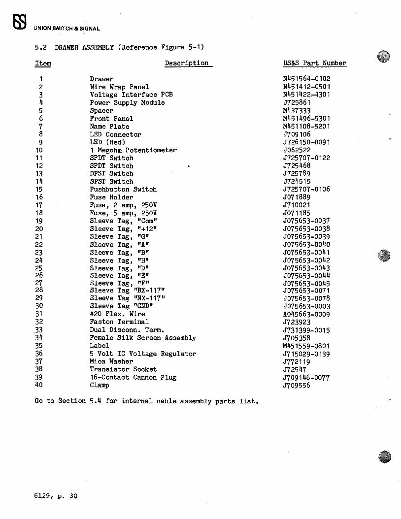
5.2 DRAWER ASSEMBLY (Reference Figure 5-1)
Item
1 2 3 4 5 6 7 8 9
10 11 12 13 14 15 16 17 18 19 20 21 22 23 24 25 26 27 28 29 30 31 32 33 34 35 36 37 38 39 40
Description
Drawer Wire Wrap Panel Voltage Interface PCB Power Supply Module Spacer Front Panel Name Plate LED Connector LED (Red) 1 Megohm Potentiometer SPOT Switch SPOT Switch DPST Switch SPST Switch Pushbutton Switch Fuse Holder Fuse, 2 amp, 250V Fuse, 5 amp, 250V Sleeve Tag, "Com" Sleeve Tag, "+12" Sleeve Tag, "G" Sleeve Tag, "A" Sleeve Tag, "B" Sleeve Tag, "H" Sleeve Tag, "D" Sleeve Tag, "E" Sleeve Tag, "F" Sleeve Tag "BX-117" Sleeve Tag "NX-117" Sleeve Tag "GND" 1120 Flex. Wire Faston Terminal Dual Disconn. Term. Female Silk Screen Assembly Label 5 Volt IC Voltage Regulator Mica Washer Transistor Socket 16-Contact Cannon Plug Clamp
Go to Section 5.4 for internal cable assembly parts list.
6129 I P• 3Q
US&S Part Number
N451564-0102 N451412-0501 N451422-4301 J725861 M437333 M451496-5301 M451108-5201 J709106 J726150-0091 J062522 J725707-0122 J725468 J725789 J724515 J725707-0106 J071889 J710021 J071185 J075653-0037 J075653-0038 J075653-0039 J075653-0040 J075653-0041 J075653-0042 J075653-0043 J075653-0044 J075653-0045 J075653-0071 J075653-0078 J075653-0003 A045663-0009 J723923 J731399-0015 J705358 M451559-0801 J715029-0139 J772119 J72547 J709146-0077 J709556
r+,-1+1 L-,;,;;-.J
----, itc:]+1 I----' .... r- --, H-C)+1 L...:---'
DODD
UNION SWITCH & SIGNAL m
J •• ---- "ON"tl3'i 1-- nNltl~d I I
L_
(PREPARED ;FROM DRAWING ;F451564•02, REV. 2)_
®
c,u • CPU I
® @) FAIL
HIP FLOP
CPU A tPU IS
VIArCH DOG UIDICATIOK
hUINUl~{R tr.\'I KAWUAL AUTO 1$1 CPU A n··iE,u A UJ'(P
SCL£CT ~ 0\IU-ltlDf ~ c, u a ·a" Pu e rrsr
[]
CPU A CPU B CPU A CPU a
@ @) @) fAI\. TltA»SfU TO
JtESET
fAIL OVER CONfROL LOGIC N4~1 564-0201
~~~~ ~
C.PU A CPU S ~A"l (@\. llK~ •,;; FU H£R
@) OEUV TUHR.
POWU @• s® .... ,,,,.
-..:!:.. ruse
6129, p. 31

m UNION SWITCH & s';GNAL
THIS PAGE INTENTIONALLY LEFT BLANK
6129, p. 32
5.3 WIRE WRAP PANEL (Reference Figure 5-2)
Board Location Description Qty.
A1 Optical Isolator 2 A2 Optical Isolator 2 A3 Optical Isolator 2 A4 Multi-Component Module 1
1330 ohm, 1/4 watt resistors: 6 A5 A6 Optical Isolator 2 A7 Optical Isolator 2 A8 Multi-Co onent Module 1
1 MFD. 20V Tantalum Ca acitor 8 A9 Multi-Com onent Module 1
2.4K ohm 1/2 watt resistors: A10 A11 5 volt, 360 ohm coil, Reed Relay 1 A12 5 volt, 360 ohm coil, Reed Relay 1 A13 5 volt, 360 ohm coil, Reed Relay 1 A14 5 volt, 360 ohm coil, Reed Relay 1 A15 A16 5 volt, 360 ohm coil, Reed Relay 1 A17 5 volt, 360 ohm coil, Reed Relay 1 A18 5 Volt, 125 Ohm Coil, Reed Relay 1 A19 5 volt, 360 ohm coil, Reed Relay 1 A20 A21 5 volt, 360 ohm coil, Reed Relay 1 A22 Multi-Com onent Module 1
200 DIV 1 am Diodes 1N4001: A23 Multi-Com anent Module 1
A24 A25
1 MFD. 35V Tantalum Ca acitors: 3
A26 5 volt, 360 ohm coil, Reed Relay 1 A27 5 volt, 360 ohm coil, Reed Relay 1 A28 5 volt, 360 ohm coil, Reed Relay 1 A29 5 volt, 360 ohm coil, Reed Relay 1 A30 5 volt, 360 ohm coil, Reed Relay 1 B1 J-K Master Slave Flip-Flop IC 1 B2 Triple 3-Input NAND Gate IC 1 B3 Hex Inverter IC 1 B4 Resistor Network Module containing 1
eight 2.2K ohm Resistors B5 Optical Isolator 2 B6 Multi-Component Module 1
100 Ohm, 1/4 watt resistors: 4 10,000 PF Ca acitor 4
B7 Quadruple 2-Input Positive AND Gate IC 1 BS Quadruple 2-Input Positive AND Gate IC 1 B9 Resistor Network Module containing 1
eight 2.2K ohm resistors B10 Module:
UNION SWITCH & SIGNAL El:)
US&S Part Number
J731433 J731433 J731433 N451411-1602 J735060j
J731433 J731433 N451411-1605 J709144-0018 N451411-1601 J721255
J726153-0046 J726153-0046 J726153-0046 J726153-0046
J726153-0046 J726153-0046 J726153-0045 J726153-0046
J726153-0046 N451411-1603 J72 555 N451 11-1702 J70 527
J726153-0046 J726153-0046 J726153-0046 J726153-0046 J726153-0046 J715029-0221 J715029-0078 J715029-0069 J735519-0253
J731433 N451411-1604 J735050 J709145-0166 J715029-0219 J715029-0219 J735519-0253
--~~~~~~~~~~~~~~~~~~~~~~--.
Optical Isolator 1 Jumper 1
J731433 J713795
6129, p. 33
UNION SWITCH Ii SIGNAL
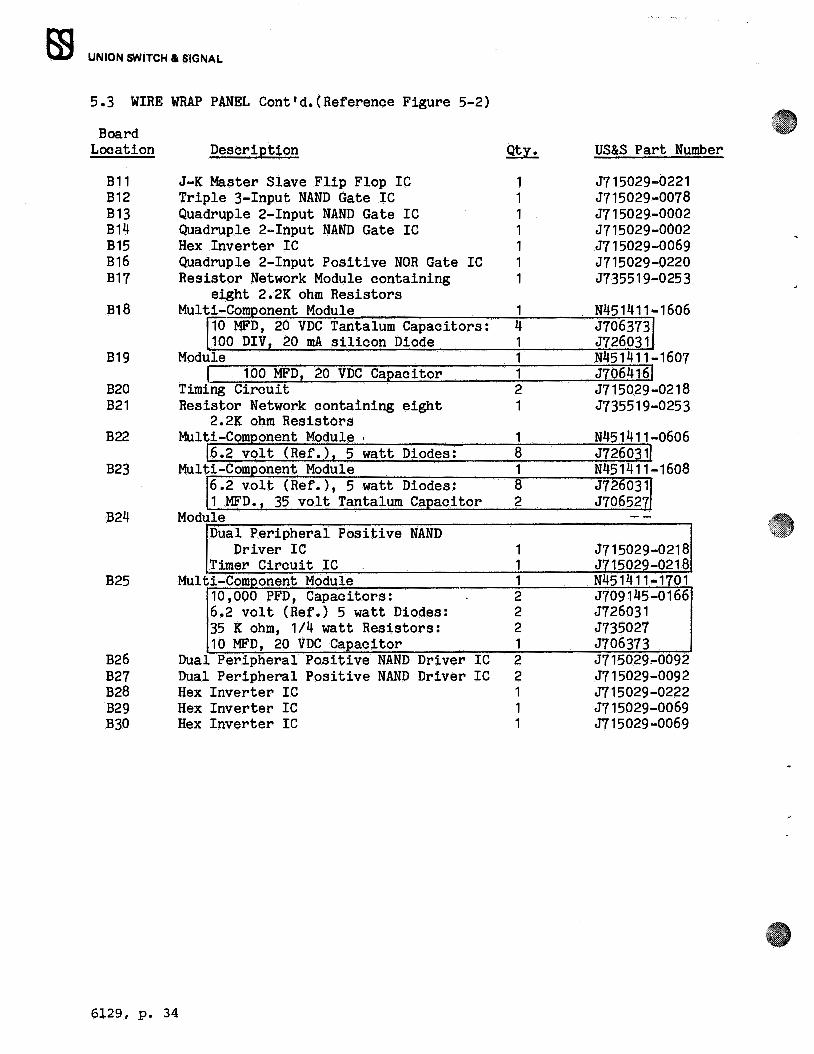
5.3 WIRE WRAP PANEL Cont'd.(Reference Figure 5-2)
Board Location Description Qty.
B11 J-K Master Slave Flip Flop IC 1 B12 Triple 3-Input NAND Gate IC 1 B13 Quadruple 2-Input NAND Gate IC 1 B14 Quadruple 2-Input NAND Gate IC 1 B15 Hex Inverter IC 1 B16 Quadruple 2-Input Positive NOR Gate IC 1 B17 Resistor Network Module containing 1
eight 2.2K ohm Resistors B18 Multi-Com onent Module 1
10 MFD, 20 VDC Tantalum Capacitors: 4 100 DIV 20 mA silicon Diode 1
B19 Module 1 I 100 MFD, 20 VDC Capacitor 1
B20 Timing Circuit 2 B21 Resistor Network containing eight 1
2.2K ohm Resistors B22 Multi-Com onent Module , 1
6.2 volt (Ref.) 5 watt Diodes: 8 B23 Multi-Com onent Module 1
6.2 volt (Ref.), 5 watt Diodes: 1 MFD. 35 volt Tantalum Ca acitor 2
B24 Module Dual Peripheral Positive NAND
Driver IC 1 Timer Circuit IC 1
B25 Mul ti-Comoonent Module 1 10,000 PFD, Capacitors: 2 6.2 volt (Ref.) 5 watt Diodes: 2 35 Kohm, 1/4 watt Resistors: 2 10 MFD, 20 VDC Capacitor 1
Dual Peripheral Positive NAND Driver IC 2 Dual Peripheral Positive NAND Driver IC 2 Hex Inverter IC 1 Hex Inverter IC 1
B26 B27 B28 B29 B30 Hex Inverter IC 1
6129, p. 34
US&S Part Number
J715029-0221 J715029-0078 J715029-0002 J715029-0002 J715029-0069 J715029-0220 J735519-0253
N451411-1606 J706373 J726031 N451411-1607 J706416! J715029-0218 J735519-0253
N451411-0606 J7260 1 N451411-1608 J72 031 J706527
J715029-0218 J715029-0218 N451411-1701 J709145-0166 J726031 J735027 J706373 J715029~0092 J715029-0092 J715029-0222 J715029-0069 J715029-0069
UNION SWITCH & SIGNAL m
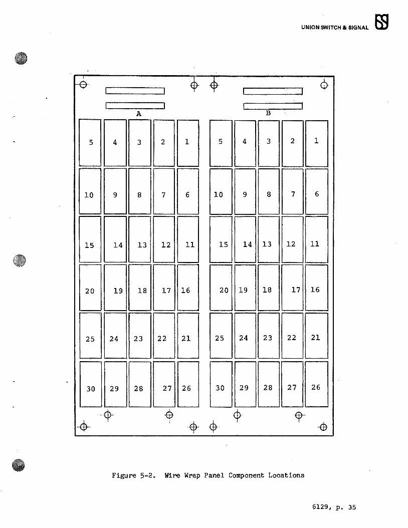
I I I l ¢--
r l I l A B
5 4 3 2 1 5 4 3 2 1
10 9 8 7 6 10 9 8 7 6
15 14 13 12 11 15 14 13 12 11
20 19 18 17 16 20 19 18 17 16
25 24 23 22 21 25 24 23 22 21
30 29 28 27 26 30 29 28 27 26
-$ i -$
Figure 5-2. Wire Wrap Panel Component Locations
6129 f P• 35

UNION SWITCH & SIGNAL
5.4 VOLTAGE INTERFACE PCB (Reference Figure 5-3) Circuit Board - A772087
Board Location
N1 ,N2,BX1 ,NX1, C,B1, E,D
PL1
V1
Cl, C4, C5
C2, C3, C6
D1
TP1 through TP8
Description
Dual Disconnect Terminal
16-Pin IC Socket
130 V RMS Metal Oxide Varistor
10 MFD, 35 WVDC Tantalum Capacitor
.001 MFD., 500 VDC Capacitor
200 PIV, 1 Amp Diode
Turret Lugs
5.5 DRAWER INTERNAL CABLE ASSEMBLIES
US&S Part Number
J731399-0015
J725840
J735524
J706625
J706242
J723555
J731396
Refer to Figure 5-4 following for internal ribbon cable configurations and part numbers.
6129, p. 36
r Nl Nl N24 N24 n ~ F=iF9F9F=i I:: :::I l:: ::I I::: ::::H::: ::I
csC :) QrP8 rr llBXl
[ I TP20 lJ~~ __j + Vl NXl
C5 WRBCC TP30b ::I 01
C :Il "-.,('"&'V«, T P4orr 11
[
C4 J C2 C + c:) lLJJ
Cl F 9 c:) [ 1+ bdB1
CJ O TP7 _J TPl Pll • 0 rr 11 TPsQ [ ) OTP5 lL JJB1
L EF =i 1 F =io :.:..I I:: ::::! b ::I
N-451522-4301
Figure 5-3. Voltage Interface PCB Component Layout
4 WIRES (SPARES)
A20
___ _____,\DO!] ON WIRE WRAP Ptj
6 WIRES 58-1901
ON WIRE WRAP PANEL7
j\._____~~ Al5
7 WIRES-
P6
PS
P7
TO FASTON N2 r VOLTAGE INTE
8 1j
"---1 WIRE
·~--2 WIRES N45145S
151458-1902 Refer to figures 6-3 through 6-5 for cable wiring diagrams
pg
Ji~ ___ m A29
PANEL~ ON WIRE WRAP Pl
L458-1903
PlO IBS
ON WIRE W'RAP PANE/ ~( m A30 P2 4 WIRES
- 4 WIRES (SPARES) N451458-
.904 I
F .j 11
I

SECTION VI SUPPLEMENTAL DATA
UNION SWITCH & SIGNAL m This edition of the service manual contains the following information, which is intended to assist in the understanding and maintenance of the Failover Control Logic:
Schematic Diagrams:
Figure 6-1. Failover Control Logic Schematic Diagram (Complete).
Figure 6-2. Voltage Interface PCB Schematic Diagram (Expanded from Figure 6-1).
Figure 6-3 Internal Cable Wiring Diagram (Including back panel connectors P.1, P2, P3, P4, P9 and Wire Wrap Panel sockets A5, A20).
Figure 6-4 Internal Cable Wiring Diagram (Including back panel connectors P5, P6, P7 and Wire Wrap Panel sockets A24, A25).
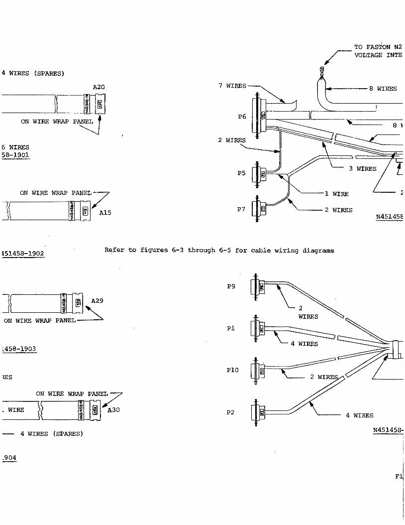
Figure 6-5 Internal Cable Wiring Diagram (Including Wire Wrap Panel sockets A15, A29, A30, socket PL1 on Voltage Interface PCB and discreet wiring to LED's switches and potentiometers).
6129, p. 39/40
1:u t7 r· r · r · f · f=- t~ t': r· r · r· r · , UNION SWITCH & SIGNAL
I I I
EB
·-·,.;:;;~,· .. :~;~t TO:~.·,: TO::.,: -=~~:~L t: •:·.~~Lt: ~~: t: ··:~AOL t: ···:~OL !: FLASHEAt:"ee>< LONE t ..... UNE t: ~~ r ______ xr __ :x: ___ x __ -x ___ :x: ___ -~.- --- --- ___ x ______ x _____ [fl_~---------------, LJ
~S9 Al•-t • Alt-t a Alt-IS I ,u:•-z J 14 """•-•• 4 13 A,is-~ IZ I\C ,-c::i _a -1
I AUTOo I 91f 81lL.__--;l:-,'l~Z~l._ __ ~l~Z~Z+---n,r·~·~·+---:t:n";--+---:b,,--+----t-'---+----t---+----t-=.:-+----t-.C.CCC-+---t--"-'--+---j--='-+-..... _..._
I I I I
~ .... 4 ..
I ~ ••• I
f (l) A.50--1 I +,a 7404
~~ ALL OPTO COUPLERS ( Alo
1-• 111cA2-Jo
'" (~,_, .. \.·~ cl'\I A I ·":~~~ I I
) AWDI J2"
{
.. ;. ··•· t ........ :JJ''"' .,_;,-. ,,.
•ATCHOOII I I INPUT I
•)----) 8WDI ::Jl PtO-t AS-4 +SA
•"' -,.- {~'~' .;~ L Rf:AOY I I lfff"UT '~
cPuY {~·:~: :::~ READY I I INl'\IT ~
- {~·:~: .:;; .... I I --
""----'"------" ..-1.:. ,.;_,
{c:D.~>;;+ ITAi I :
,.,__ ___ ,,, "'iiir ~ .. Jll-1 A5-I
Cl"UA ~ I
,.,.:~~~HT ~-17 AU~
I I I i,.~·· ....... I I
::~~T C>---;!_, AH~.·"'' I ~··-~ ... ,,s I I I '"""' I I
I I cPU·e· I I ,~:..iN:uT ~ ~
sr:u:cT IN~T ,.,_
I I
Cl'U ... ... I I ~N::.~~t·:;:,:C>---;t_, All~
FIE\.D'A OH LINE IHl'\IT
MAINTAINER CONTROL SWITOt
STOP
' .. z.zx .. ... . ..
Z,2K
"
... "" ..
>r--t------;.'-<~) : q,.cuN11tH .... s.(-)~
DRAWING 0451321-0101, REV 3
... . ...
~+SA
CPU A MOTl,AILl:0
CPu ·a· NOT/,.AILIEO
Figure 6-1.
Cl'U 'A" P'AIJ..
(:ll'U 0
8° FAI
Cf'U ... OH LINE
Failrver
)
I I ·~~
AI0-1 PS-t I I I I ·,,--····-----,
AH-4 P4-t
I I
.uo~ ... -:.7 I I
.-:ut2.' • ...~, I I
AFL ,, , Al:4-11 ,.,.....,,
I) o ) .;:;7il I PS-I
I I
I "'j' , ---,
AH-II ,.,,z
""- ,..,:. ... ~ .. I I ''-~-"'
1.1,c .·,-------, AIO-S "1-1
I 9
I .-.zt.?.. .,4 I I I I
... I I .ui~,o---.-, ...
I I
CPU °"' LINE FAILED } I
Control Logic Schematic Diagram
6129, p. 41/42

UNION SWITCH & SIGNAL ffi
&. TP-2
P&-A-tlXI 17 ::! BXI ~ . TO FUSE HOLDER
M.o.v. TP-3 r &. ,r
PB-B-NXI 17 )) fNxil » . TO A.c. ON P.s.
Pa-G-GND ~r----------------------------------------...f ~ TP-4 5V REii (ON CHASSIS) _t----:--._--------~i:>!>-----• TO CHASSIS GROUND
&. FROM -1-12 ON P.s. )) , I
&. .QOIMFO
DISC CER 600V
FROM COMM ON p.s.
)) £ TP-7
tW I &.
TP-8 &.
~' ff16 PS-F
"'
&.
D451321-0301, REV 1
TP-1
I OMFD
r
~6C5r~ 35V OC TANT ALU
Bl
Bl
,---, ~~~~~~~-j--~~~-
~ P - 5
l
+SA TO DRAM!R LED'S
LM309K
I ... ,... 2
CASE I
NI!
SV REG. (ON CHASSIS)
LM309K
+se 2
CASE)
Nlr L (NOT o:::: -~
D
&.
E
&.
DISC. CER. TANTALUM c21--~~:o c,I _L-1-!~~
+1 IOMFD
C4I35VOC TANTALUM DISC. CER.
.001
CJ I- 600V
,& DUAL FASTON TERMINAL ON P.c.q.
Figure 6-2.
tP-6
I I' l> I • } +SA TO WIRE WRAP PANEL
16 PIN DIP CONNECTOR JI
WRAP PANEL
J • COMMON ~O WI PE
+ I'")) I
} +SB TO WI RE WRAP PANEL
'---""F:....;l~~')-.j.1--•
PB-H OUT (NH)
.,------ - A2S-f 6, I, f 5,2, 14 ,3, 13,4
Voltage Interface PCB Schematic Diagram
6129, p. 43/44
© I
'1 ®
®
@ )
I ©
@ I
DRAWER
P9' 9 WAY I --6 -
Pl 9 WAY
2 -7 --3 -8 -
PIO 9 WAY
I -
6 -
P2 9 WAY
2 -7 -
3 -
8 --
. - - ....... I --6 -2 - ' 7 -3 -8 --
P4 9 WAY
I -6 --2 --7 --3 --8 -
(4) SPARE { @ CPU "A" INPUTS FROM DIGITAL I/0
@ CPU "B" INPUTS FROM DIGITAL I/0
© CPU "A" OUTPUTS TO DIGITAL I/0
@ CPU "B" OUTPUTS TO DIGITAL I/0
® c:i?u "A" AND "B" INPUTS
® CPU "A" AND "B" OUTPUTS
(4) SPARE{
UNION SWITCH & SIGNAL m I 6 P I N D I P (A 5)
GND I 6 Awnt I GNO
A RFADY I 5
GND. 2 14
ATBJ GNO
3 i I 3
BWOl i (·1.00?) GND
4
BREADY 12
GNO 5 I I STAI
SPARE i 6 10
®
SPARE" i SPARE
7
SC>AC>s:' i 9 8
i ! PREPARED FROM DRAWING ' : 0451321-0201
' I
I '
GND I I 6 CPU A FAIL i I
(A20)
GNO I 5 CPU B FAIL 2 GND I 4 CPU A ON LINE 3 GNO I 3
4 (-1,01) 11
CPU A FAIL GND I 2 CPU B FA II 5 GND I I CPU BON LINE 6 SPARE I O SPARF' 7 SPARE 9 SPARE 8
i
®
I Figure 6-3. Internal Cable Wiring Diagram
(Inc. Pl, P2, P3, P4, P9, to AS, A20)
6129, p. 45/46

PS 25 WAY I --14 -2 -
I 5 --3 --
16 -4 -
I 7 5
18 --6 --
@ 19 -J 7 -
20 8 --
2·1 -9 -
22 .
IO -23 -I I --24 12
.. -25 -I 3 -
PS 9 WAY
.2 i -6, -
® ) . , ' -
I"
P7 9 WAY
I . -6 -
I G)
(B24 POWER TO CONSOLE) (7) ~8 STANDARD WIRES
~u To· POINT A ON 824 FUSE
l ' ' ~ ' ' ' . '
(e) WIRES TO N24-PCB FASTON (N24 SUPPLY TO WIRE WRAP PANEL)
i j j j II ' I
@ TO CONSOLE
@ TO T-BAR DRIVER
G) TO VR-4, CPU ON-LINE FAIL IND.
0 CONSOLE INPUTS
~ CONSOLE OUTPUTS
(3) SPARE
UNION SWITCH & SIGNAL m
I 16 PIN DIP ( N24 I 6 N24 N24 I
N24 I I 5 2 N24 14 N24
N24 3
N24 I 3
CPU A FAIL RI SET INPUT 4 (-1.001) I 2 .
CPU B FAlL RI SET INPOT FI ELO A SELEC T INPUT 5
FI ELD B SELE.I T INPUT I I 6
FI t: -D A ON-L NE INPUT FIE O B ON-L NE IO INPUT STD HUMP" 51( iNAL
7
GND 9 8
A25)
0
I
i
PREPARED FROM DRAWING ! 0451321-0201
A FAIL LAMP B FAIL IAUP
XFR TO A LAMf XFR TO S I .AMf A RF'.ADY I .AMP , 8 RE'AOV I AUP I
A ON LINE LAMP BON LINE LAMP FAIL BE• I f'AIL BELL T BAR DRIVER CPU ON LINC. f'l\ll CPU ON LINE FA IL SPAR£ SPARE SPARE . .
I
I 6 PIN DIP (, I 6 ARE' I I 5 . 2 14 3 13 4 (•"2001) I 12 5 II 6 10 7 9 8
Figure 6-4. Internal Cable Wiring Diagram (Inc. PS, P6, P7, to A24, A25)
6129, p. 47/48