failure modes and low temperature performance of dc/dc ... modes an… · failure modes and low...
TRANSCRIPT
National Aeronautics and Space Administration
Failure Modes and Low Temperature Performance of DC/DC Converters
Rosa Leon Jet Propulsion Laboratory
Pasadena, California
Jet Propulsion Laboratory California Institute of Technology
Pasadena, California
JPL Publication 09-36 12/09


National Aeronautics and Space Administration
Failure Modes and Low Temperature Performance of DC/DC Converters
NASA Electronic Parts and Packaging (NEPP) Program
Office of Safety and Mission Assurance
Rosa Leon Jet Propulsion Laboratory
Pasadena, California
NASA WBS: 724297.40.43 JPL Project Number: 103982
Task Number: 03.02.05
Jet Propulsion Laboratory 4800 Oak Grove Drive
Pasadena, California 91109
http://nepp.nasa.gov
ii
This research was carried out at the Jet Propulsion Laboratory, California Institute of
Technology, and was sponsored by the National Aeronautics and Space Administration
Electronic Parts and Packaging (NEPP) Program.
Reference herein to any specific commercial product, process, or service by trade name,
trademark, manufacturer, or otherwise, does not constitute or imply its endorsement by the
United States Government or the Jet Propulsion Laboratory, California Institute of Technology.
Copyright 2009. California Institute of Technology. Government sponsorship acknowledged.

iii
TABLE OF CONTENTS ABSTRACT ........................................................................................................................ 1 I. INTRODUCTION ....................................................................................................... 2 II. EXPERIMENTAL DETAILS ..................................................................................... 2
A. Efficiency, Regulation, Cross-regulation, Regulation with Capacitive Loads, and Power Consumption with Inhibit and No Load ............................................ 6
B. Load Transient Response ..................................................................................... 6 C. Synchronization ................................................................................................... 8 D. Turn-on ................................................................................................................ 9
III. RESULTS DISCUSSION ......................................................................................... 10 A. Efficiency and Regulation as a Function of Temperature ................................. 10 B. Turn-on Below -55°C ........................................................................................ 11 C. Load Transient Response Below -55°C ............................................................ 18 C. Synchronization Below -55°C ........................................................................... 25 D. Output Current vs. Input Voltage and Efficiency .............................................. 30
IV. SUMMARY .............................................................................................................. 33 V. REFERENCES .......................................................................................................... 34 VI. APPENDIX A ........................................................................................................... 35

1
ABSTRACT Several standard tests to evaluate key (direct current) DC/DC converter parameters were performed on different models of hybrid radiation-hard DC/DC converters. These tests were done to assess both performance and reliability during space applications that operate the converters at temperatures below the lower military range of -55°C. One of the converters failed near -110°C, but another DC/DC converter model started normally at temperatures as low as -140°C. The latter showed acceptable performance during turn-on, load transient, and synchronization tests even though, some minor anomalies were observed. These results show good promise for its use in applications where the DC/DC converters will be operated at lower temperatures.
An application circuit was also built and preliminary tests were performed on a commercial (low drop out) LDO type of DC to DC converter with adjustable output voltage. These can be used in point of load (POL) applications. This latter device functioned properly on the few tests that were performed; however, more testing is needed to identify potential issues with space use of this and similar devices.

2
I. INTRODUCTION The work described in this report is a result of tests performed under the FY09 NEPP task “Failure modes, reliability and performance of DC to DC converters.” This task is the continuation of the FY08 NEPP task with the same title. Several of these tests were designed during the performance of a large inter-center task sponsored by the NASA Engineering and Safety Center (NESC) in FY06 and FY07 to develop recommendations for specifying parameters and test methods for DC to DC converters. A comprehensive test matrix was generated by the NESC converter team, encompassing needs identified at various NASA centers [1].
This present task aimed to evaluate reliability of some commercial models of DC/DC converters since failures due to low temperature operation were observed in the FY08 task. One of these failures looked very similar to a failure that was seen during testing in a recent flight application [2, 3]. Furthermore, significant differences in the low temperature performance of these devices were also observed, and these observations warranted further work concerning their reliability at low temperatures.
The experimental set up needed to evaluate the reliability of the newer point of load (POL) converters was also established during performance of this task.
II. EXPERIMENTAL DETAILS
DC/DC Converters Tested Tests were performed on radiation hard DC/DC converters that have been used in multiple flight applications and are still being used in flight hardware. Regulators were selected to span a broad range of powers and applications in digital and analog signals as well as mixed signal applications. Three devices from two different manufacturers were used. JPL does not intend to endorse one manufacturer over other vendors; the selection shown here does reflect a range in applications, and it is an attempt to address potential reliability concerns on some of the DC/DC hybrid converters and POL regulators that are used in multiple flight applications. Due to our limited time/resources, products from only two manufacturers were tested in this report. However, future test efforts will include products from other manufacturers as well.
Converter E (part name: ARH2812S) is a 30-watt output, positive 12V single output hybrid DC/DC converter, manufactured by International Rectifiers Inc. and used in analog applications. One hundred percent load was set for 2.5 amps for the 12V output.
Converter or regulator H (part name: MSK5810RH) is a radiation-hard (to 450K rad) drop out adjustable linear regulator that will take from 2V to 7.5V input voltage and can provide output voltages ranging from 1.5V to 7V; it is manufactured by M. S. Kennedy. Typical applications include field programmable gate arrays (FPGAs).
Another converter, DC/DC converter B (Part name: ART2815T also from IR), was also examined. Uses of this converter include mixed signal, redundancy, and special applications. To give a short summary, this would have continued work from FY08 where this converter failed upon seeing operating temperatures below -110°C [3]. The failure was due to voltage overstress on the output capacitor as the pulse width modulator (PWM) circuit malfunctioned and the output voltage (48V) exceeded the rated voltage of the output capacitor (35V). The output capacitors were replaced with the same value/footprint capacitor but rated for 50V. Converter B

3
was tested but found to be open; therefore, more work should be done to implement this strategy. This could enable work to make certain models of commercially, available radiation-hard converters capable of withstanding extremely low temperatures, and it is one of the approaches that will be pursued in future work. Tests Performed The following tests were performed on converter E at temperatures below -55 C:
• Load regulation • Efficiency • Transient load response • Synchronization • Turn-on
The following tests were performed on converter H (POL converter) at room temperature:
• Output current vs. input voltage
• Efficiency vs. input voltage and output currents
Temperature Control and Monitoring Hybrid DC/DC converters were tested at room temperature using a finned heat sink. A small fan was also used to lower the temperature when the converters were fully powered up. Thermocouples were T-type. They were mounted on thermal tape between the heat sink and the converters with a plate bolted on the converters to make good thermal contact.
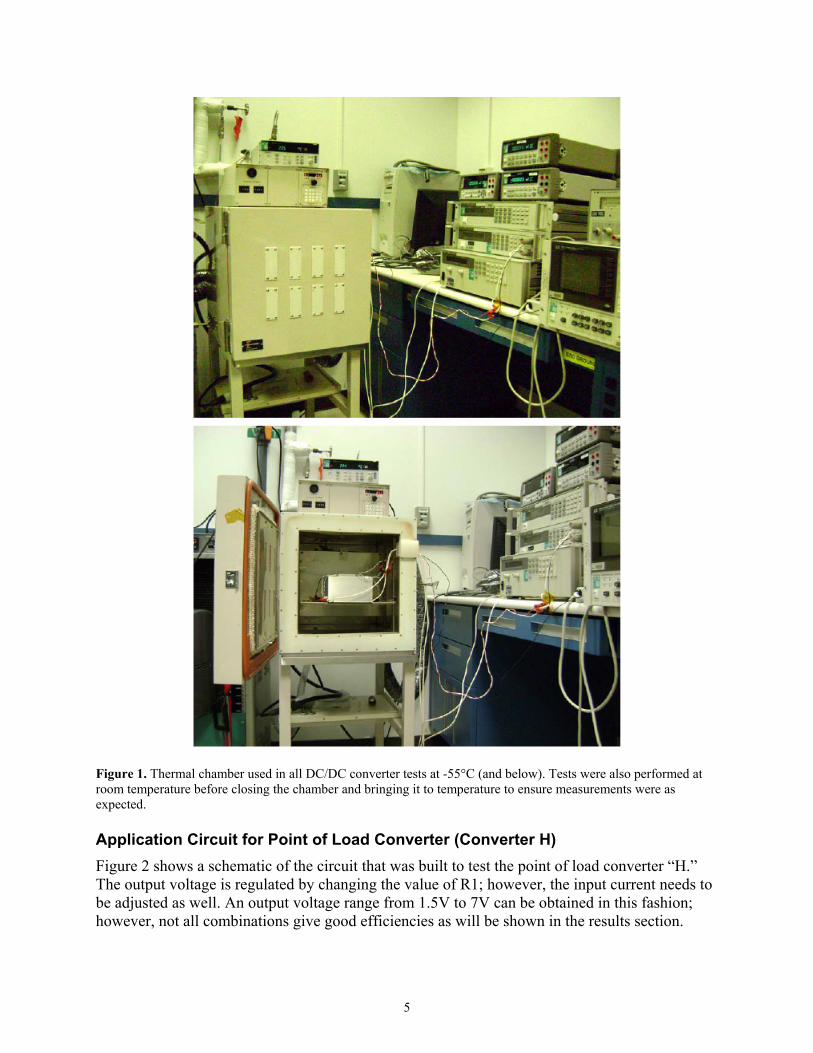
When tests were performed at and below -55°C, a Sigma Systems M30 computer controllable thermal chamber was used. The system’s testing capabilities include both cycling and static temperature testing at extreme temperatures from -175°C to 250°C. With small thermal masses, the chamber achieved a ramp rate between temperatures above 10°C/min. Inert atmosphere testing was achieved through a built-in gas purge (using nitrogen). Adjustable, fail-safe, over-temperature and under-temperature protection was built into the system and is active in both manual operation and remote operation. Secondary redundant, fail-safe apparatuses were installed for flight parts testing. The test chamber is 33cm (L) x 25cm (W) x 33cm (H) and has eight 7.6cm x 1.3cm door feed troughs and one 5cm side port. Figure 1 shows the chamber both closed and with a converter inside ready for tests. Manual control was used in these tests since the device thermocouple temperature was used (rather than the chamber thermocouple reading). At full load there was sometimes a small discrepancy, so the chamber temperature was adjusted accordingly.
Temperatures were recorded for the DC measurements, and other measurements were performed only when the real temperature (as read by the thermocouple) was within positive or negative 2°C of the nominal temperatures. The thermal chamber can achieve closer temperature control (easily within one-half of a degree), but the thermal margins stated were used to perform the tests in a more timely manner.
Safety Precautions • Wear electrostatic discharge (ESD) straps and ESD coat.

4
• Disable output from power supply when not using.
• Do not turn converter on without some load (at least 10%).
• Make sure input wires are rated to take input current (important for higher power converters).
• To prevent the converter from going into oscillation mode, make sure that enough voltage and current are supplied as the power supply is turned on. Do not gradually turn on power supply (except when explicitly required by the stated test condition, as in one type of turn-on test) but, rather, set to minimum (or higher) voltage stated in specification sheet and use the converter’s inhibit function or an input switch so the converter is instantly turned on rather than gradually turned on.
Test Equipment Used
• HP 6060B 3-60V and 0-60A-300W electronic loads (as many as converter outputs)
• HP 6654A DC power supply (stable and provides enough power for the 96-watt converters)
• Temperature controller (data acquisition switch unit) Agilent 34970A
• FLUKE 77 Series II multimeter (only for monitoring)
• Agilent 34401A digital multimeter (for measurements)
• Switch (field effect transistor [FET] or mercury) and small power supplies as needed for switch (only for start-up tests)
• Pulse generator: HP 8112A (only for synchronization tests)
• Oscilloscope: Tektronix TDS 3014B (for start up, synchronization, and load transient response tests)
• Precision resistors (one for each output and one for the input current measurements) Dale 0.1 ohm (50 watts) for testing this converter
• Capacitor boards (101 uFarad chip capacitors) and electrolytic capacitors
• Heat sinks and thermocouple (to regulate and monitor temperature)
• Agilent 4395A network/spectrum/impedance analyzer and Ridley frequency analyzer (for stability margins tests)
• Thermal chamber to perform measurements at -55°C and at 125°C
• Current probe: Tektronix (AM 503 current probe amplifier)
5
Figure 1. Thermal chamber used in all DC/DC converter tests at -55°C (and below). Tests were also performed at room temperature before closing the chamber and bringing it to temperature to ensure measurements were as expected. Application Circuit for Point of Load Converter (Converter H) Figure 2 shows a schematic of the circuit that was built to test the point of load converter “H.” The output voltage is regulated by changing the value of R1; however, the input current needs to be adjusted as well. An output voltage range from 1.5V to 7V can be obtained in this fashion; however, not all combinations give good efficiencies as will be shown in the results section.

6
Figure 2. Application circuit built to test point of load converter (provided in the manufacturer’s data sheet). The output voltage is controlled by replacing R1 with different value resistors while leaving R2 fixed. The output current is also adjusted to obtain the desired output voltage for a given input voltage.
A. Efficiency, Regulation, Cross-regulation, Regulation with Capacitive Loads, and Power Consumption with Inhibit and No Load
Efficiency of a converter is defined as: % efficiency = 100 * (Power out/Power in). Regulation is defined as: % regulation = 100 * (Vout any load - Vout nominal)/(Vout nominal). A slightly different definition for voltage regulation is used in datasheets. To avoid confusion, the voltage regulation is given as a straight voltage value in the figures presented in this report. The set-up for these measurements is illustrated in Figure 3.
All measurements were done for the three values of input voltage: minimum, nominal, and maximum (set by the vendor’s datasheet). For converter E, they are 18V, 28V, and 50V.
B. Load Transient Response This test determines the relative performance of the converter’s feedback circuitry. This test also gives a qualitative indication of the adequacy of stability design margins with respect to the converter’s feedback loop design. The test set-up diagram to evaluate the converter’s response to a transient load is shown in Figure 4.
Slew rates between the two loads should be as fast as possible and need to be faster than 1A per 1µS. The electronic load’s fastest slew rate should be fast enough to handle this (as an example, agilent loads can switch up to 5A per µS; other manufactures’ loads may be used).
With the intent to simulate some flight applications that use DC/DC converters with very small loads, this test was changed to also include low load step transient response. In this case, the

7
fixed output was kept at 50%, but the pulsed output was pulsed from 5% to 50% in the single output hybrid converter that was tested. Results from this test at low temperature are also shown in this report.
Figure 3. Set-up diagram for efficiency, voltage regulation, and cross-regulation measurements. Wire lengths were 2–3 feet; gauges were 18 or 22 feet for smaller signals.
Figure 4. For the load transient response measurements. For a single output converter, the single load is pulsed from 25% to 50%. For dual output converters, one load is pulsed and the other load is kept constant. Both outputs are monitored on oscilloscope, and voltage overshoot and recovery times are measured. For dual output converters, loads are as follows: regular load—one side 50%, the other side pulsed from 25% to 50%; low load—one side 50%, the other side pulsed from 2.5% to 25%. For a triple output converter, two loads are kept constant at 33%, while the output being tested is pulsed from 10% to 33%. If capacitors are included they are in parallel with the output that is being pulsed.
8
The input voltages tested were low, nominal, and high per vendor datasheets.
The test was configured by connecting the output to an oscilloscope. Even if only one output is pulsed, in dual output converters, both outputs will have a small voltage overshoot. The tests were done at the different resistance loads described previously.
The electronic load (we are using HP 6060B) was programmed so that loads can be pulsed. The scope traces were collected at a couple different time scales. Measurements of voltage overshoot and recovery times are evident from these scope traces.
When any anomaly was seen performing this test, collecting information on the actual current transients (we used the Tektronix AM 503 current probe amplifier) brought valuable insight. Depending on the nature of the irregularity, current waveforms should be collected at the input and both outputs (or at minimum the pulsed output). This was done with this converter for low load transient response tests since some anomalies were observed. Figure 4 shows a diagram for this test set-up.
C. Synchronization This test verifies that the output voltage is synchronized with a pulse of a certain frequency (per vendor datasheet) when the unit locks to an external synchronization signal.
For converter E, the synchronization range is between 225 and 310 KHz (per vendor datasheet). A diagram of this test set-up is shown in Figure 5.
To perform the test, the output of a pulse generator (square wave, 50% duty cycle, 4.5 ns rise and fall times) is connected to the synch signal input pin. The outputs are monitored on an oscilloscope, and the pulse generator waveform and the converter’s output waveform are measured. Traces from the pulse generator waveform and both outputs are collected at a couple of representative time scales for each voltage input, load, frequency, and signal amplitude tested. Low and high signal amplitude are 3.5V and 10V , respectively.
Scope traces were collected only for the following conditions: 28V input, 100% loads, lowest and highest allowed (per datasheet) signal pulse, and minimum and maximum frequencies per each converter.

9
Figure 5. This test verifies that the output voltage is synchronized with an external pulse of a certain frequency. Synchronization for converter D is 500 to 700 KHz; for converter B it is 225 to 275 KHz; and for converter C it is 500 to 600 KHz (per vendor datasheets).
D. Turn-on A diagram for these tests is shown in Figure 6. Turn-on comprises four different tests:
1. The first test has the power source on with the converter first inhibited and then uninhibited. This was done for minimum, nominal, and maximum input voltages.
2. The second test applies the input voltage to the converter using a switch. Either an FET or a mercury switch may be used. Since Hg switches are permitted at the Jet Propulsion Laboratory (JPL), Hg switches were used when bounceless switches were required. Input power (voltage) and the converter output(s) are recorded on an oscilloscope simultaneously. This measures the delay time to achieve full regulation as well as any voltage overshoots. This test was performed for all three input voltages.
3. The third test is similar to the second test but uses an input switch circuit that has a few milliseconds delay ramp. Two of these circuits were designed, and tests were repeated using large capacitors in parallel with the input power. However, these oscillations still persisted for some conditions, probably due to the inherent resistance of the switch. A recent meeting and information exchange with the vendors indicated that these tests were expected to be performed using the inhibit release function after the converter was fully powered up. Vendor datasheets do not specify this test condition, and reconciling test methods/flight applications/vendor datasheets is still in progress [1].

10
4. The fourth test is to determine at what voltage the converter starts to regulate. A voltage ramp is required and needs to be slow enough to determine when the converter starts. This particular test was done manually, since the turn-on is too slow to be captured on an oscilloscope. After ramp-up and turn-on, the input voltage to the converter is ramped down and the voltage at which the converter turns off is noted. This test, by its nature, can only be done near the minimum voltage, and it is done at both full load and minimum load. Minimum load was arbitrarily chosen as 10% for the tests shown here.
Due to limited testing time, only the second test (rapid or bounceless switch turn-on) were performed in this task and are presented in this report.
Figure 6. Set-up diagram for turn-on tests.
III. RESULTS DISCUSSION
A. Efficiency and Regulation as a Function of Temperature Figure 7 shows the results of testing both efficiency and regulation as a function of temperature for converter E. The efficiency was tested using 28V input and at 50% load, which is the most “benign” condition. Performing the same test with a wider variety of loads and the minimum and maximum input voltages would be a valuable test and might uncover additional problems that would not surface under the benign test conditions used here.

11
The efficiency peaks at 0°C and maintains over 80% down to -55°C. It drops to 76% at the point right above the lowest operating temperature of this converter; however, most applications can probably tolerate this relatively small drop in efficiency.
Regulation values are plotted as voltage values to avoid confusion over the different definitions used by different vendors on voltage regulation formulas. The value of regulation drops slightly down to -100°C and rises again, reaching the maximum value at the lowest temperature where the converter will still function (turn-on). This particular converter initially had a higher voltage value than stated in the data sheet. Extensive tests on this converter showed that this is not a problem as far as regulator performance in other areas and for its sustained reliable operation.
70
72
74
76
78
80
82
12
12.5
13
13.5
14
-150 -100 -50 0 50
Efficiency and voltage regulationat 50% load and 28V input
efficiency at 50% load and 28V input
regulation
effic
ienc
y (in
%) regulation (V
olts)
temperature Figure 7. Efficiency and regulation at 50% load for converter E as a function of temperature. Measurements spanned the thermal range -150°C (fails to turn-on) to 35°C, but results up to 125°C were obtained and are shown in previous reports.
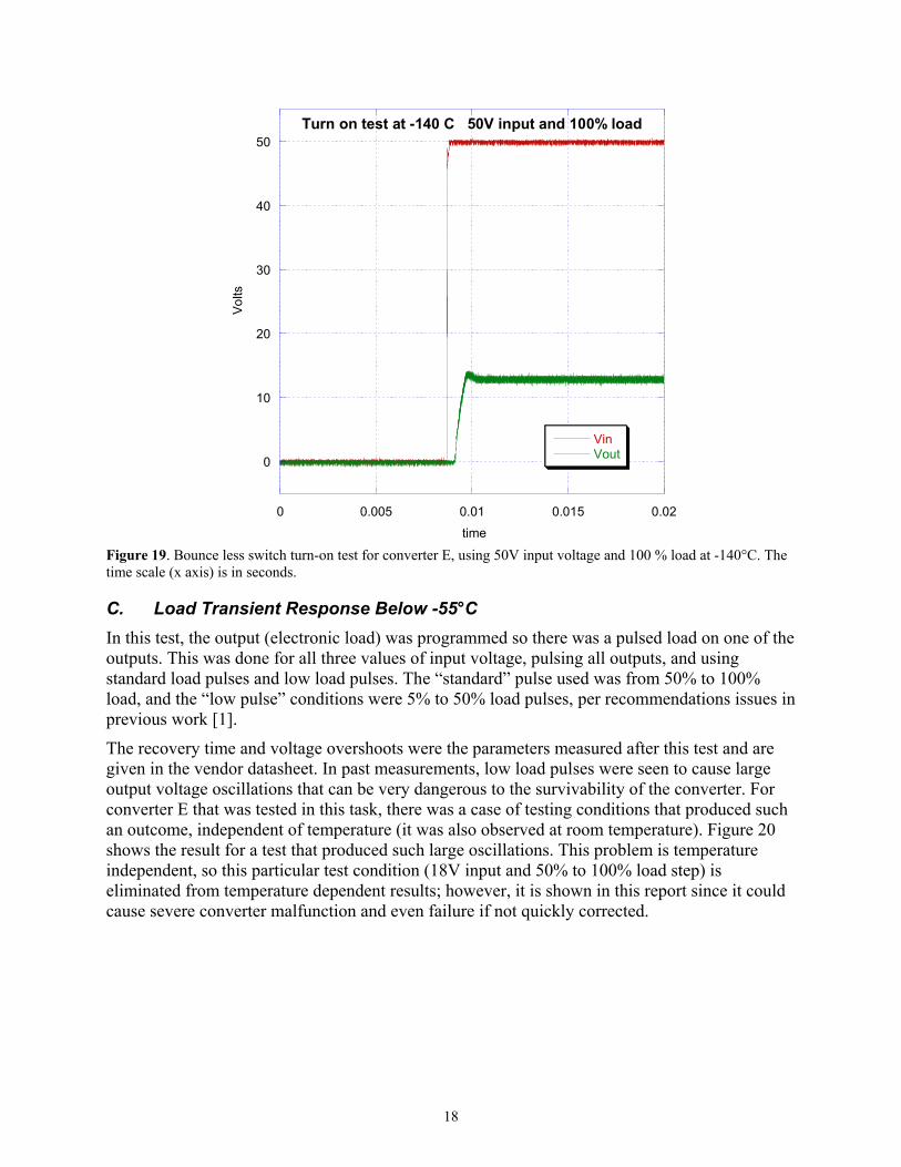
B. Turn-on Below -55°C Turn-on tests on converter E showed that the converter can turn on normally below -140°C but fails to turn on at -150°C. The measurements were made with the converter in the thermal chamber as described previously in Section II. The recommended EMI filter for this converter was used; the filter was also in the thermal chamber and kept at the same temperature as the converter. Scope traces were collected for two values of load (10% and 100%) and three values of input voltage (19V, 28V [nominal], and the maximum of 50V). Data was taken at 15°C and

12
20°C temperature interval, giving scope traces from -55°C, 70°C, 85°C, 100°C, 120°C, and 140°C.
Figures 8–13 show all cases of input voltages and loads tested at the next to highest test temperature (-70°C), and Figures 14–19 show the same tests performed at the lowest end of the thermal scale that gave good turn-on test results, -140°C. Scope traces taken between -85°C and -120°C do not show significant difference and are shown in Appendix A.
As described in Section II, a complete turn-on test for a DC/DC converter includes other more complete types of tests that were omitted due to time constraints. Evaluating turn-on with a slow switch ramp would be valuable in this case, as it is the condition most prone to turn-on anomalies. These include ‘false starts’ seen in previous measurements [3, 4]. However, the results shown here indicating normal turn-on as low as -140°C are very promising for use of this particular converter model in high reliability, low temperature applications. Further testing for turn-on characteristics of this converter below -55°C would be very valuable in order to ensure reliable operation of this unit at the low temperatures often encountered in space flight and testing.
0
10
20
30
40
50
0 0.005 0.01 0.015 0.02
Turn on test at -70°C18 V input and 10% load
VinVout
Volts
time
Figure 8. Bounceless switch turn-on test for converter E, using minimum input voltage and 10 % load at -70°C. The time scale (x axis) is in seconds.

13
0
10
20
30
40
50
0 0.005 0.01 0.015 0.02
Turn on test at -70°C18 V input and 100% load
VinVout
Vol
ts
time
Figure 9. Bounceless switch turn-on test for converter E, using minimum input voltage and 100% load at -70°C. The time scale (x axis) is in seconds.
0
10
20
30
40
50
0 0.005 0.01 0.015 0.02
Turn on test at -70°C28 V input and 10% load
VinVout
Vol
ts
time Figure 10. Bounceless switch turn-on test for converter E, using nominal (28V ) input voltage and 10% load at -70°C. The time scale (x axis) is in seconds.

14
0
10
20
30
40
50
0 0.005 0.01 0.015 0.02
Turn on test at -70°C28 V input and 100% load
VinVout
Vol
ts
time Figure 11. Bounceless switch turn-on test for converter E, using 28V input voltage and 100% load at -70°C. The time scale (x axis) is in seconds.
0
10
20
30
40
50
0 0.005 0.01 0.015 0.02
Turn on test at -70°C50 V input and 10% load
VinVout
Volts
time Figure 12. Bounceless switch turn-on test for converter E, using 50V input voltage and 10% load at -70°C. The time scale (x axis) is in seconds.

15
0
10
20
30
40
50
0 0.005 0.01 0.015 0.02
Turn on test at -70°C50 V input and 100% load
VinVout
Vin
time Figure 13. Bounceless switch turn-on test for converter E, using 50V input voltage and 100% load at -70°C. The time scale (x axis) is in seconds.
0
10
20
30
40
50
0 0.005 0.01 0.015 0.02
Turn on test at -140°C18 V input and 10% load
VinVout
Vol
ts
time Figure 14. Bounceless switch turn-on test for converter E, using 18V input voltage and 10% load at -140°C. The time scale (x axis) is in seconds.

16
-10
0
10
20
30
40
50
0 0.005 0.01 0.015 0.02
Turn on test at -140°C18 V input and 100% load
VinVout
Volts
time Figure 15. Bounceless switch turn-on test for converter E, using 18V input voltage and 100% load at -140°C. The time scale (x axis) is in seconds.
0
10
20
30
40
50
0 0.005 0.01 0.015 0.02
Turn on test at -140°C28 V input and 10% load
VinVout
Volts
time Figure 16. Bounceless switch turn-on test for converter E, using 28V input voltage and 10% load at -140°C. The time scale (x axis) is in seconds.

17
0
10
20
30
40
50
0 0.005 0.01 0.015 0.02
Turn on test at -140°C28 V input and 100% load
VinVout
Vol
ts
time (seconds) Figure 17. Bounceless switch turn-on test for converter E, using 28V input voltage and 100% load at -140°C. The time scale (x axis) is in seconds.
0
10
20
30
40
50
0 0.005 0.01 0.015 0.02
Turn on test at -140 C 50 V input and 10% load
VinVout
Vol
ts
time Figure 18. Bounceless switch turn-on test for converter E, using 50V input voltage and 10% load at -140°C. The time scale (x axis) is in seconds.
18
0
10
20
30
40
50
0 0.005 0.01 0.015 0.02
Turn on test at -140 C 50V input and 100% load
VinVout
Volts
time Figure 19. Bounce less switch turn-on test for converter E, using 50V input voltage and 100 % load at -140°C. The time scale (x axis) is in seconds.
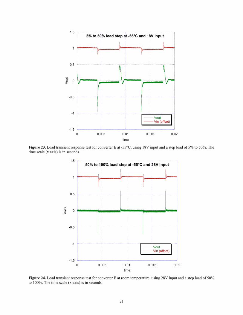
C. Load Transient Response Below -55°C In this test, the output (electronic load) was programmed so there was a pulsed load on one of the outputs. This was done for all three values of input voltage, pulsing all outputs, and using standard load pulses and low load pulses. The “standard” pulse used was from 50% to 100% load, and the “low pulse” conditions were 5% to 50% load pulses, per recommendations issues in previous work [1].
The recovery time and voltage overshoots were the parameters measured after this test and are given in the vendor datasheet. In past measurements, low load pulses were seen to cause large output voltage oscillations that can be very dangerous to the survivability of the converter. For converter E that was tested in this task, there was a case of testing conditions that produced such an outcome, independent of temperature (it was also observed at room temperature). Figure 20 shows the result for a test that produced such large oscillations. This problem is temperature independent, so this particular test condition (18V input and 50% to 100% load step) is eliminated from temperature dependent results; however, it is shown in this report since it could cause severe converter malfunction and even failure if not quickly corrected.

19
-12
-10
-8
-6
-4
-2
0
2
4
0 0.005 0.01 0.015 0.02
50% to 100% load step at -55C and 18V input
Vin (offset)Vout
Volts
time Figure 20. Load transient response test that gave anomalous results, shown here as large output voltage oscillations. These were seen at all temperatures (including room temperature) and are not related to temperature but, rather, are due to these particular conditions making the converter unstable. These are shown for converter E, using 18V input and a step load of 50% to 100%. These conditions result in oscillations regardless of temperature, so only this plot is shown. The time scale (x axis) is in seconds.
Measurements of load transient response were performed for room temperature and below -55C down to -145C in increments of 10, 15, and 20 degrees. Two load conditions were used, from 50% to 100% and from 5% to 50%. Input voltages used were 18V, 28V and 50V.
Figures 21 and 22 show the two types of step load transient response curves at room temperature and 28V input voltages. These are useful for comparison with the low temperature scope traces. Figure 23 shows results for the test performed at -55°C for a 5% to 50% load step and 18V input voltage, and Figure 24 shows the test results for a “normal” load step of 50% to 100% load also at -55°C and 28V input. The low load test is shown for 28V input at the same temperature in Figure 25, while Figures 26 and 27 show the same information for -55°C and 50V input voltage.
The datasheet for this converter states a maximum voltage overshoot of 200mV and a maximum recovery time of 200 µs. When the low load transients are applied, both voltage overshoot values and recovery times are larger and longer. However, even though this converter does not quite meet performance specifications under these conditions, it continues to operate normally and does not go into an abnormal large output voltage oscillation mode (except in the case of 18V input and 50% to 100% step load).

20
-1.5
-1
-0.5
0
0.5
1
1.5
0 0.005 0.01 0.015 0.02
50% to 100% load step at 20C and 28V input
Vin (offset)Vout
Vin
time Figure 21. Load transient response test for converter E at room temperature, using 28V input and a step load of 50% to 100%. The time scale (x axis) is in seconds.
-1.5
-1
-0.5
0
0.5
1
1.5
0 0.005 0.01 0.015 0.02
5% to 50% load step at 20°C and 28V input
VoutVin (offset)
Volts
time Figure 22. Load transient response test for converter E at room temperature, using 28V input and a step load of 5% to 50%. The time scale (x axis) is in seconds.
21
-1.5
-1
-0.5
0
0.5
1
1.5
0 0.005 0.01 0.015 0.02
5% to 50% load step at -55°C and 18V input
VoutVin (offset)
Vou
t
time Figure 23. Load transient response test for converter E at -55°C, using 18V input and a step load of 5% to 50%. The time scale (x axis) is in seconds.
-1.5
-1
-0.5
0
0.5
1
1.5
0 0.005 0.01 0.015 0.02
50% to 100% load step at -55°C and 28V input
VoutVin (offset)
Volts
time Figure 24. Load transient response test for converter E at room temperature, using 28V input and a step load of 50% to 100%. The time scale (x axis) is in seconds.

22
-1.5
-1
-0.5
0
0.5
1
1.5
0 0.005 0.01 0.015 0.02
5% to 50% load step at -55°C and 28V input
VoutVin (offset)
Volts
time
Figure 25. Load transient response test for converter E at - 55°C, using 28V input and a step load of 5% to 50%. The time scale (x axis) is in seconds.
-1.5
-1
-0.5
0
0.5
1
1.5
0 0.005 0.01 0.015 0.02
50% to 100% load step at -55°C and 50V input
VoutV in (offset)
Vou
t
time Figure 26. Load transient response test for converter E at - 55°C, using 50V input and a step load of 50% to 100%. The time scale (x axis) is in seconds.

23
-1.5
-1
-0.5
0
0.5
1
1.5
0 0.005 0.01 0.015 0.02
5% to 50% load step at -55°C and 50V input
VoutVin (offset)
Vout
time Figure 27. Load transient response test for converter E at room temperature, using 28V input and a step load of 5% to 50%. The time scale (x axis) is in seconds.
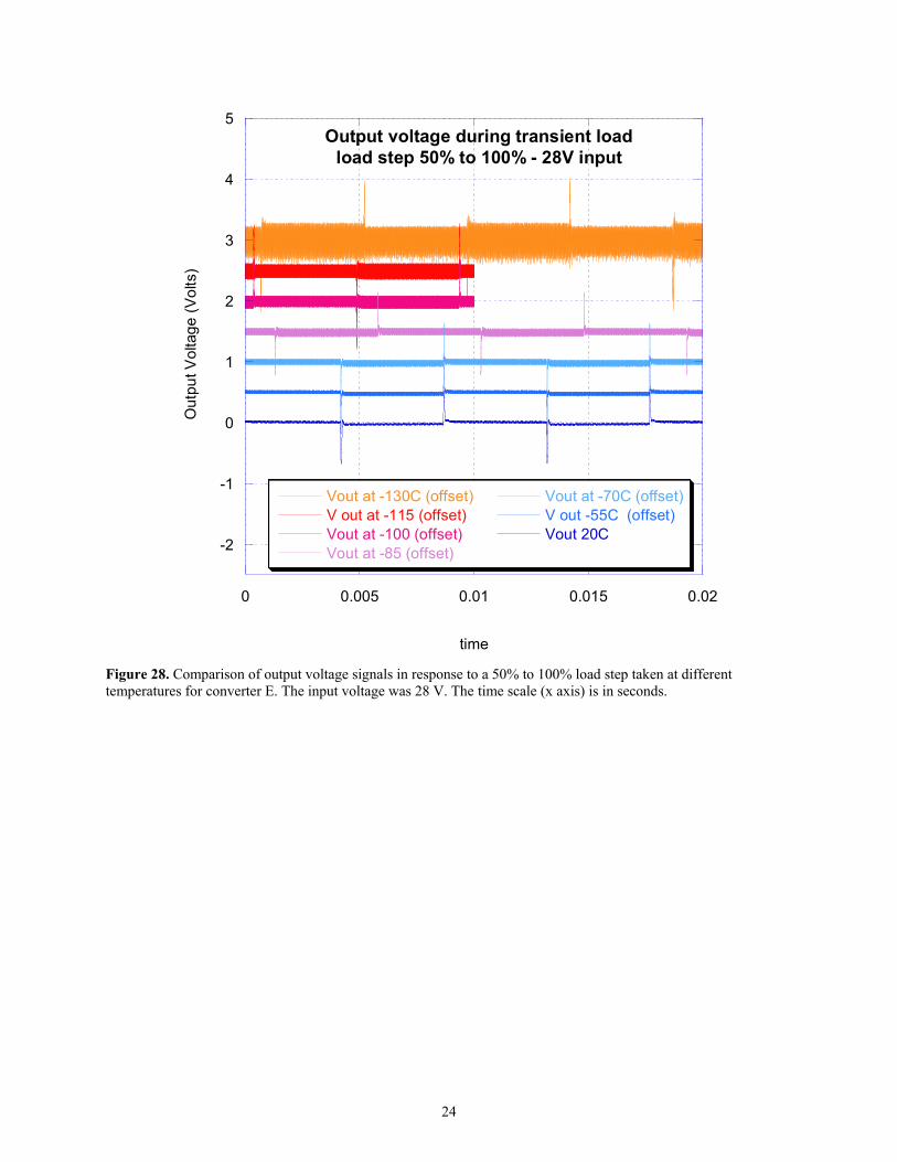
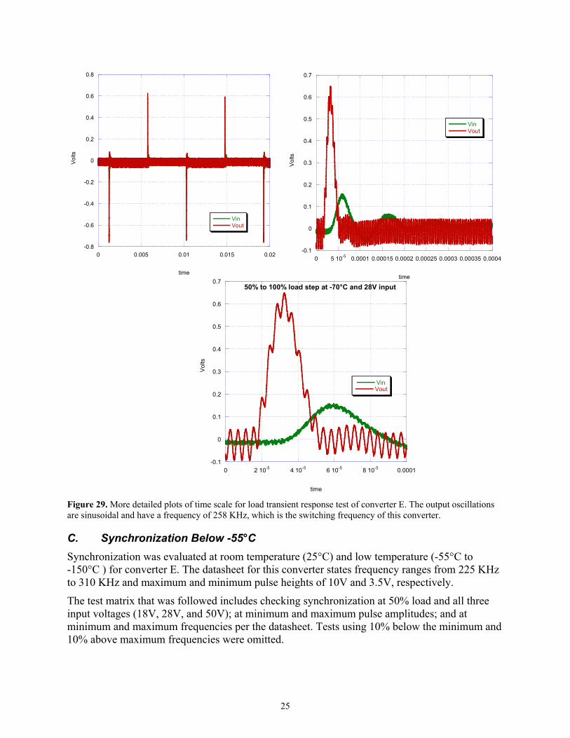
Comparisons of these test results show that at lower temperatures we see an apparent “noise” in the output signal. This is even more apparent as the temperature is lowered, as shown in Figure 28, which shows a segment of the output voltage from room temperature down to -130°C. As can be seen, the noise-like signal progressively increases with decreasing temperature. Further analysis shows that these fluctuations or “fuzziness” in the output voltage are not really noise. Figure 29 shows progressively more detail on the time axis for a load transient response plot for a 50% to 100% load step and 50V input taken at -70°C. Rather, the signal that increases with decreasing temperature is sinusoidal. The frequency of this signal is 258 KHz, which is the switching frequency of this converter. Since the effective resistance of the output capacitor is known to increase with decreasing temperature, the voltage drop (IR) for a given current signal will become increasingly larger as the temperature is reduced. This hypothesis needs further experimental and modeling verification; however, it qualitatively explains the results quite well.
These test results show that converter E responds to a transient load as low as -145°C and, despite the increase in the output sinusoidal signal at 258 KHz, the converter performs well.
24
-2
-1
0
1
2
3
4
5
0 0.005 0.01 0.015 0.02
Output voltage during transient loadload step 50% to 100% - 28V input
Vout at -130C (offset)V out at -115 (offset)Vout at -100 (offset)Vout at -85 (offset)
Vout at -70C (offset)V out -55C (offset)Vout 20C
Out
put V
olta
ge (V
olts
)
time Figure 28. Comparison of output voltage signals in response to a 50% to 100% load step taken at different temperatures for converter E. The input voltage was 28 V. The time scale (x axis) is in seconds.
25
-0.8
-0.6
-0.4
-0.2
0
0.2
0.4
0.6
0.8
0 0.005 0.01 0.015 0.02
VinVout
Volts
time
-0.1
0
0.1
0.2
0.3
0.4
0.5
0.6
0.7
0 5 10-5 0.0001 0.00015 0.0002 0.00025 0.0003 0.00035 0.0004
VinVout
Vol
ts
time
-0.1
0
0.1
0.2
0.3
0.4
0.5
0.6
0.7
0 2 10-5 4 10-5 6 10-5 8 10-5 0.0001
50% to 100% load step at -70°C and 28V input
VinVout
Vol
ts
time Figure 29. More detailed plots of time scale for load transient response test of converter E. The output oscillations are sinusoidal and have a frequency of 258 KHz, which is the switching frequency of this converter.
C. Synchronization Below -55°C Synchronization was evaluated at room temperature (25°C) and low temperature (-55°C to -150°C ) for converter E. The datasheet for this converter states frequency ranges from 225 KHz to 310 KHz and maximum and minimum pulse heights of 10V and 3.5V, respectively.
The test matrix that was followed includes checking synchronization at 50% load and all three input voltages (18V, 28V, and 50V); at minimum and maximum pulse amplitudes; and at minimum and maximum frequencies per the datasheet. Tests using 10% below the minimum and 10% above maximum frequencies were omitted.

26
A good performing synchronization function will show good correlation between the pulse wave (incoming) and the synchronization glitch in the voltage output signal. Examples of conditions that gave good synchronization performance are shown at room temperature in Figure 30 and at -143°C in Figure 31. As these indicate, good synchronization can be achieved below -140°C for some cases. The larger sinusoidal signal from the output voltage is related to what was described in the load transient response discussion and it is caused by the increase in effective series resistance of the output capacitor with decreasing temperature.
-0.8
-0.6
-0.4
-0.2
0
0.2
0.4
0.6
-6
-4
-2
0
2
4
6
0 5 10-6 1 10-5 1.5 10-5 2 10-5
Synch test at 225KHz and high pulse50% load, 50V input at 23°C
Vout Pulse
Vol
tsP
ulse Voltage
time Figure 30. Synchronization at room temperature using high pulse and 225 KHz frequency in converter E. The input voltage was 50 V. The measurement in the oscilloscope was set for AC.

27
-0.8
-0.6
-0.4
-0.2
0
0.2
0.4
0.6
-6
-4
-2
0
2
4
6
0 1 10-5 2 10-5
Synch test at 225KHz and high pulse50% load, 50V input at -143°C
Vout Pulse
Volts
Pulse Voltage
time Figure 31. Synchronization at -143°C using high pulse and 225 KHz frequency in converter E. The input voltage was 50 V. The measurement was made with the AC (alternating current) setting in the oscilloscope.
While the plots on Figures 30 and 31 show good performance, and converter E synchronized under all conditions all the way down to -143°C, some anomalies were observed, even at room temperature. The test results showed that even though synchronization is successful, larger scale oscillations are also present. Sometimes these larger oscillations are severe and the converter shows some instabilities. Figure 32 shows a case of this anomaly at room temperature. At low temperatures, this malfunction was more common and, if it was observed, it was usually more severe. Converter E can still be synchronized at temperatures as low as -143°C under some conditions, but it is a narrower set of conditions as the converter’s operating temperature drops. Figure 33 shows an example of this malfunction or anomaly for a test performed at -143°C. Notice the y scale on the right (the output voltage scales) indicating the larger voltage oscillations at low temperature. In Table 1, a summary is presented of all conditions tested at room temperature (23°C), -55°C, -100°C, and -143°C.
As seen in Table 1, some conditions do not cause voltage instability at any of the measured temperatures. These are 18V input at 225 KHz and high pulse; 28V input, 225 KHz and high pulse; 50V input, 225 KHz and high pulse; and, most likely, 28V input, 225 KHz and low pulse (measurement still needed for room temperature to confirm the latter). Some cases of faulty

28
synchronization seemed to synch normally at lower temperatures under the same conditions of pulse, frequency and input voltage, so it is very difficult to make predictions on the other conditions; more work is needed to accurately predict and provide a good understanding of synch as a function of temperature. As stated above, tests performed in the past [3, 4] that included 10% below the minimum recommended frequency and 10% above the maximum recommended frequency were not done in this task, since these give faulty results even at room temperature, at least for this model converter.
-0.4
-0.2
0
0.2
0.4
-6
-4
-2
0
2
4
6
0 5 10-6 1 10-5 1.5 10-5 2 10-5
Synch test at 310KHz and low pulse50% load, 18V input at 23°C
Vout
Pulse
Vol
tsP
ulse
time Figure 32. Synchronization test at -23°C (room temperature) using low pulse and 225 KHz frequency in converter E. The input voltage was 18 V. The measurement was made with the AC (alternating current) setting in the oscilloscope.

29
-0.8
-0.6
-0.4
-0.2
0
0.2
0.4
0.6
0.8
-6
-4
-2
0
2
4
6
0 5 10-6 1 10-5 1.5 10-5 2 10-5 2.5 10-5 3 10-5 3.5 10-5 4 10-5
Synch test at 225KHz and low pulse50% load, 50V input at -143°C
Vout Pulse
Vol
tsP
ulse
time Figure 33. Synchronization at -143°C using low pulse and 225 KHz frequency in converter E. The input voltage was 50 V. The measurement was made with the AC (alternating current) setting in the oscilloscope. Table 1. Results for synchronization in converter E at various temperatures. Faulty synchronization does not indicate failure to synchronize, since synch was good for all conditions at all temperatures tested. Rather, it indicates that the test resulted in large output voltage fluctuations that could result in unstable conditions, as shown in Figures 30 and 31.
Temperature Test conditions Room (23°C) -55°C -100°C -143°V 18V input 225KHz Low pulse
Good synchronization
Faulty synchronization
Good synchronization
Faulty synchronization
18V input 225KHz High pulse
Good synchronization
Good synchronization
Good synchronization
Good synchronization
18V input 310KHz Low pulse
Faulty synchronization
Faulty synchronization
Faulty synchronization
Good synchronization

30
Temperature Test conditions Room (23°C) -55°C -100°C -143°V 18V input 310KHz High pulse
Good synchronization
Good synchronization
Good synchronization
Faulty synchronization
28V input 225KHz Low pulse
Not measured Good synchronization
Good synchronization
Good synchronization
28V input 225KHz High pulse
Good synchronization
Good synchronization
Good synchronization
Good synchronization
28V input 310KHz Low pulse
Not measured Faulty synchronization
Faulty synchronization
Faulty synchronization
28V input 310KHz High pulse
Good synchronization
Good synchronization
Faulty synchronization
Faulty synchronization
50V input 225KHz Low pulse
Good synchronization
Good synchronization
Faulty synchronization
Faulty synchronization
50V input 225KHz High pulse
Good synchronization
Good synchronization
Good synchronization
Good synchronization
50V input 310KHz Low pulse
Good synchronization
Good synchronization
Faulty synchronization
Faulty synchronization
50V input 310KHz High pulse
Good synchronization
Good synchronization
Faulty synchronization
Faulty synchronization
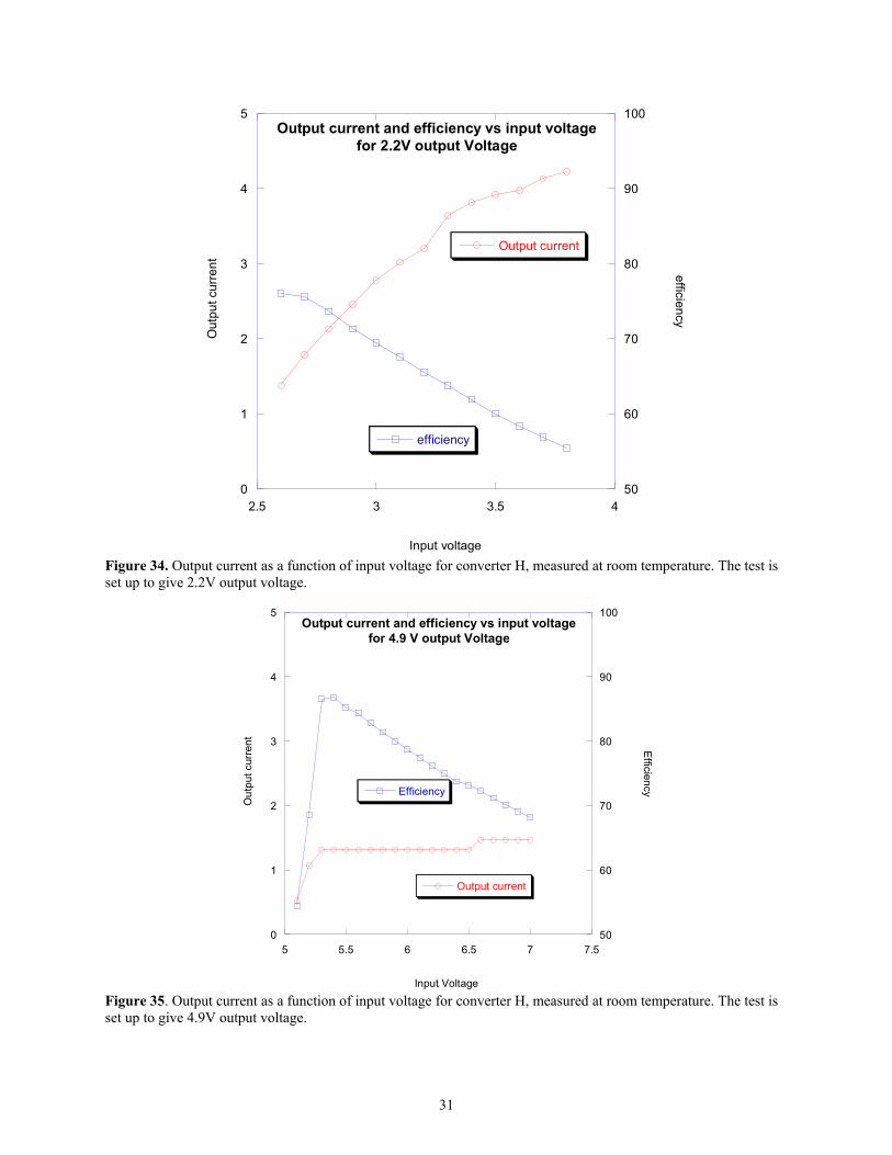
D. Output Current vs. Input Voltage and Efficiency
These tests pertain to the LDO regulator, converter H. An application circuit was built (shown in Figure 2). In this device, the output voltage is regulated by changing the value of R1; however, the input current needs to be adjusted as well. An output voltage range from 1.5V to 7V can be obtained in this fashion; however, not all combinations give good efficiencies, as shown in Figures 34–36. Measurements were made for input voltage combinations that give 2.2V output, 4.9V output, and 1.35V output. These were obtained with output resistor values (R2) of 976 ohms, 2,940 ohms, and 187 ohms, respectively. Plots of output current and efficiency (second y axis) vs. input voltages are shown in Figures 34, 35, and 36, respectively. These different values in output voltage give flexibility in the input voltage used; however, as seen in this plots, the efficiency drops as the input voltage is raised. Another concern, besides lower efficiency, is higher heating of the POL converter. Heat sinking should be used in this application to maintain device operation near room temperature.
31
0
1
2
3
4
5
50
60
70
80
90
100
2.5 3 3.5 4
Output current and efficiency vs input voltage for 2.2V output Voltage
Output current
efficiency
Out
put c
urre
nt efficiency
Input voltage Figure 34. Output current as a function of input voltage for converter H, measured at room temperature. The test is set up to give 2.2V output voltage.
0
1
2
3
4
5
50
60
70
80
90
100
5 5.5 6 6.5 7 7.5
Output current and efficiency vs input voltage for 4.9 V output Voltage
Output current
Efficiency
Out
put c
urre
nt Efficiency
Input Voltage Figure 35. Output current as a function of input voltage for converter H, measured at room temperature. The test is set up to give 4.9V output voltage.

32
0
1
2
3
4
5
20
30
40
50
60
70
80
90
100
1.5 2 2.5 3 3.5 4
Output current and efficiency vs input voltage for 1.45 V output Voltage
Output Current
Efficiency
Out
put C
urre
nt Efficiency
Input Voltage
Figure 36. Output current as a function of input voltage for converter H, measured at room temperature. The test is set up to give 1.45V output voltage.

33
IV. SUMMARY Converters have failed at low temperature in flight applications even when the mission temperature requirements were relatively benign [5]. In this work, such failures were reproduced [3], but other models have found to survive lower temperatures and even perform most basic functions under cryogenic conditions. This indicates important underlying differences in the reliability of such hybrid converters at low temperatures. Testing below -55°C indicates that some models of DC/DC hybrid converters can withstand temperatures below -140°C, thus facilitating insertion of these commercial devices into flight systems that will require lower thermal bounds. Measurements on a chosen converter model indicate that its efficiency is still 94% of its maximum value (at 0°C) and the regulation is not negatively affected by the cryogenic environment. Other findings from these tests results include the observation of a sinusoidal component to the output voltage from the hybrid DC/DC converter tested that increased as the temperature was reduced. This sinusoidal component has the switching frequency of the converter and is most likely related to the increase in effective resistance from the output capacitor that occurs at low temperature. This increased sinusoidal output voltage component might contribute to some of the anomalies seen during synchronization testing; however, it was also observed that both load transient response and synchronization can work at temperatures as low as -143°C even though specs from the datasheet are not met under these conditions. Testing of a commercial linear low drop out point of load (POL) converter was set up, and performance tests were started. Measurements of output current and efficiency vs. input voltage were made, showing that this device has a good amount of flexibility but the efficiency drops considerably as the input voltage drops. Care must be taken to heat sink the device, due to the large heat dissipated when low input voltages are low. Further testing is needed to uncover potential reliability concerns that could surface with space applications of this and other models of POL converters.
34
V. REFERENCES [1] Barr, Cunningham, Facto, Nieraeth, Plante, Rutledge, Sharma, Shue, and Vorperian,
NASA Guidelines for Selection and Applications of DC/DC Converters, May 2008. [2] Nguyen, T., MSL Interpoint converter application WCA guidelines and user’s guidelines,
Rev. A, 2 May 2007. [3] R. Leon, final report for FY09 NEPP task: “DC to DC Converter Testing for Space
Applications: Use of EMI Filters and Thermal Range of Operation,” October 2008. [4] Leon, R., JPL Inter Office Memorandum 5145-08-002. [5] Plante, J., DC/DC Converters User Database, NEPP site (http://nepp.nasa.gov).

35
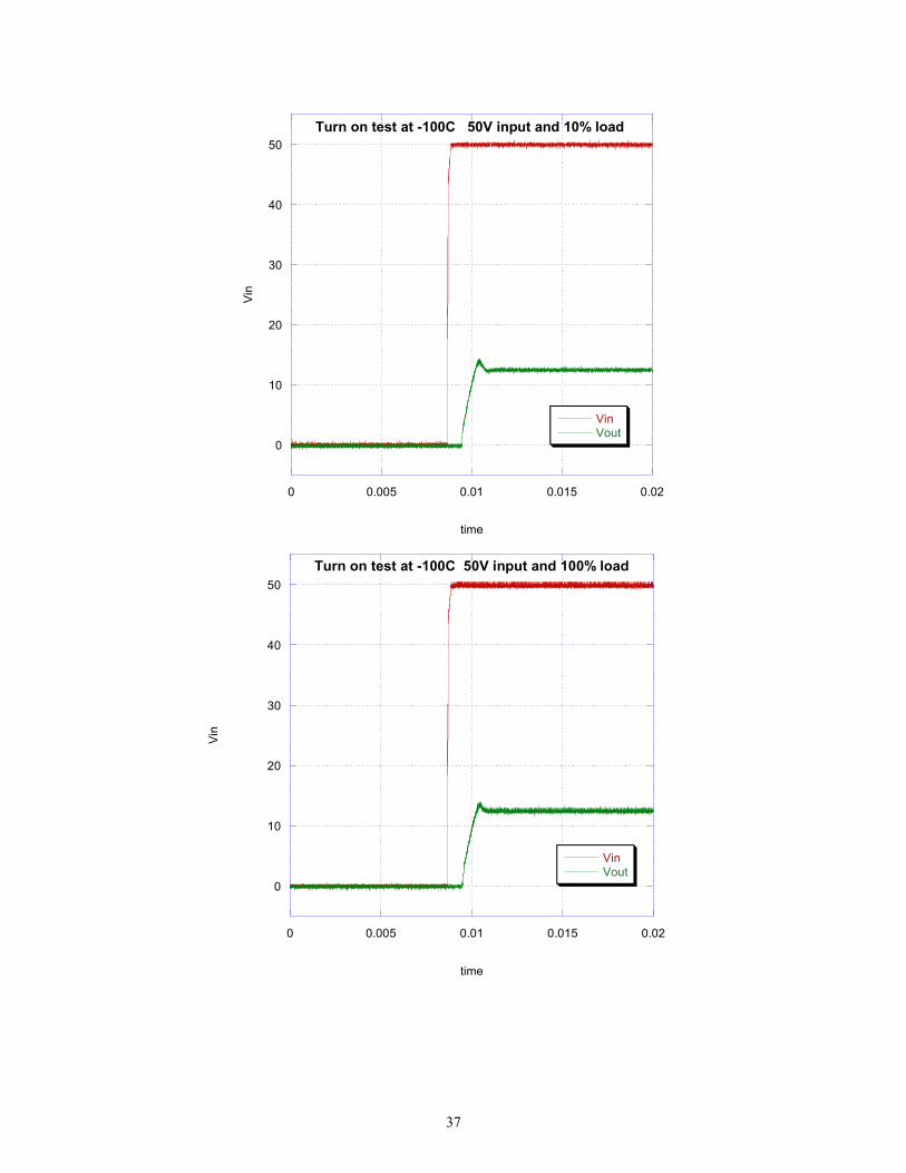
VI. APPENDIX A Turn-on test data for converter E at temperatures -85 C to -120 C. Input voltages and load conditions are specified on the top of each curve.
0
10
20
30
40
50
0 0.005 0.01 0.015 0.02
Turn on test at -85 C18V input and 10% load
VinVout
Vol
ts
time
0
10
20
30
40
50
0 0.005 0.01 0.015 0.02
Turn on test at -85 C18V input and 100% load
VinVout
Vol
ts
time

36
0
10
20
30
40
50
0 0.005 0.01 0.015 0.02
Turn on test at -85C - 50V input and 10% load
VinVout
Volts
time
0
10
20
30
40
50
0 0.005 0.01 0.015 0.02
Turn on test at -100 C28V input and 100% load
VinVout
Vol
ts
time
37
0
10
20
30
40
50
0 0.005 0.01 0.015 0.02
Turn on test at -100C 50V input and 10% load
VinVout
Vin
time
0
10
20
30
40
50
0 0.005 0.01 0.015 0.02
Turn on test at -100C 50V input and 100% load
VinVout
Vin
time

38
0
10
20
30
40
50
0 0.005 0.01 0.015 0.02
Turn on test at -120 C18V input and 10% load
VinVout
Vin
time
0
10
20
30
40
50
0 0.005 0.01 0.015 0.02
Turn on test at -120 C18V input and 100% load
VinVout
Vol
ts
time

39
0
10
20
30
40
50
0 0.005 0.01 0.015 0.02
Turn on test at -120C 50V input and 10% load
VinVout
Volts
time
0
10
20
30
40
50
0 0.005 0.01 0.015 0.02
Turn on test at -120C 50V input and 100% load
VinVout
Vol
ts
time