faux vector processor design using fpga-based …bailey/tm16.pdf · faux vector processor design...
TRANSCRIPT
Faux Vector Processor Design
Using FPGA-Based Cores
by
Diwas Timilsina
A thesis submitted in partial fulfillment
of the requirements for the
Degree of Bachelor of Arts with Honors
in Computer Science
Williams College
Williamstown, Massachusetts
May 22, 2016
Contents
1 Introduction 1
2 Previous Work 42.1 E�ciency Comparison Between GPPs, FPGAs, and ASICs . . . . . . . . . 4
2.2 The Return of the Vector Processor . . . . . . . . . . . . . . . . . . . . . . 6
2.3 Performance- and Power-Improving Designs . . . . . . . . . . . . . . . . . . 12
2.4 GPP-FPGA Communication . . . . . . . . . . . . . . . . . . . . . . . . . . 14
2.5 Power Consumption Analysis on FPGA . . . . . . . . . . . . . . . . . . . . 17
2.6 Summary . . . . . . . . . . . . . . . . . . . . . . . . . . . . . . . . . . . . . 18
3 The FPGA Work Flow 203.1 Field Programmable Gate Array Architecture . . . . . . . . . . . . . . . . . 21
3.2 Architecture Supporting Partnered Communication . . . . . . . . . . . . . . 23
3.3 FPGA reconfiguration workflow . . . . . . . . . . . . . . . . . . . . . . . . . 24
3.3.1 Typical Application: Dot Product of Vectors . . . . . . . . . . . . . 24
3.3.2 Describing the Circuit . . . . . . . . . . . . . . . . . . . . . . . . . . 24
3.3.3 Simulation . . . . . . . . . . . . . . . . . . . . . . . . . . . . . . . . 26
3.3.4 Synthesis and Implementation . . . . . . . . . . . . . . . . . . . . . 27
3.4 Summary . . . . . . . . . . . . . . . . . . . . . . . . . . . . . . . . . . . . . 27
4 Faux-Vector Processor 284.1 FVP Architectural Overview . . . . . . . . . . . . . . . . . . . . . . . . . . 29
4.1.1 Interface . . . . . . . . . . . . . . . . . . . . . . . . . . . . . . . . . . 29
4.1.2 Instruction Set Architecture . . . . . . . . . . . . . . . . . . . . . . . 31
4.1.3 FPGA Implementation . . . . . . . . . . . . . . . . . . . . . . . . . 35
4.2 Programming the FVP from Processing System . . . . . . . . . . . . . . . . 37
4.2.1 Design Examples . . . . . . . . . . . . . . . . . . . . . . . . . . . . . 37
4.3 Summary . . . . . . . . . . . . . . . . . . . . . . . . . . . . . . . . . . . . . 43
5 Faux-Vector Processor Performance Estimation 455.1 Methodology . . . . . . . . . . . . . . . . . . . . . . . . . . . . . . . . . . . 45
5.2 Hardware Utilization . . . . . . . . . . . . . . . . . . . . . . . . . . . . . . . 45
5.3 Vector Performance . . . . . . . . . . . . . . . . . . . . . . . . . . . . . . . . 46
5.4 Benchmark Performance . . . . . . . . . . . . . . . . . . . . . . . . . . . . . 53
5.5 Power Analysis . . . . . . . . . . . . . . . . . . . . . . . . . . . . . . . . . . 60
i
CONTENTS ii
5.6 Summary . . . . . . . . . . . . . . . . . . . . . . . . . . . . . . . . . . . . . 62
6 Future Work 636.1 Improving Faux-Vector Processor Design . . . . . . . . . . . . . . . . . . . . 63
6.1.1 Upgrading Memory Interface Unit . . . . . . . . . . . . . . . . . . . 63
6.1.2 Broadening the Functionality . . . . . . . . . . . . . . . . . . . . . . 64
6.1.3 Multiple Lane Extension . . . . . . . . . . . . . . . . . . . . . . . . . 64
6.1.4 Integration with a Vector Compiler . . . . . . . . . . . . . . . . . . . 64
6.1.5 Automating Circuit Design and Synthesis . . . . . . . . . . . . . . . 65
6.2 Improving Performance Estimation . . . . . . . . . . . . . . . . . . . . . . . 65
6.2.1 Improved Power Analysis and Optimization . . . . . . . . . . . . . . 65
6.3 Open Challenges . . . . . . . . . . . . . . . . . . . . . . . . . . . . . . . . . 66
7 Conclusions 67
Acronyms 68
Bibliography 70
List of Figures
1.1 40 Years of trend in microprocessor data . . . . . . . . . . . . . . . . . . . . 2
2.1 GPP datapath energy breakdown . . . . . . . . . . . . . . . . . . . . . . . . 5
2.2 Di↵erence between scalar and vector Processor . . . . . . . . . . . . . . . . 7
2.3 The block diagram of VIRAM . . . . . . . . . . . . . . . . . . . . . . . . . . 8
2.4 The block diagram of CODE . . . . . . . . . . . . . . . . . . . . . . . . . . 8
2.5 The block diagram of Soft Core Processor . . . . . . . . . . . . . . . . . . . 10
2.6 VESPA architecture with two lanes . . . . . . . . . . . . . . . . . . . . . . . 11
2.7 The RSVP architecture . . . . . . . . . . . . . . . . . . . . . . . . . . . . . 12
2.8 Diagram of a c-core chip . . . . . . . . . . . . . . . . . . . . . . . . . . . . . 13
2.9 The block diagram of LegUp design . . . . . . . . . . . . . . . . . . . . . . 14
2.10 The block diagram of RIFFA architecture. . . . . . . . . . . . . . . . . . . . 15
2.11 Diagram of PuspPush Architecture . . . . . . . . . . . . . . . . . . . . . . . 16
3.1 Picture of Zedboard . . . . . . . . . . . . . . . . . . . . . . . . . . . . . . . 20
3.2 Picture of FPGA . . . . . . . . . . . . . . . . . . . . . . . . . . . . . . . . . 22
3.3 Xillybus overview . . . . . . . . . . . . . . . . . . . . . . . . . . . . . . . . . 23
3.4 Implemented circuit diagram . . . . . . . . . . . . . . . . . . . . . . . . . . 26
4.1 Block diagram of FVP architecture . . . . . . . . . . . . . . . . . . . . . . . 35
4.2 Memory Interface Unit . . . . . . . . . . . . . . . . . . . . . . . . . . . . . . 36
5.1 Resource utilization of hardware implementation with and without FVP . . 46
5.2 Performance of VLD instruction . . . . . . . . . . . . . . . . . . . . . . . . 48
5.3 Performance of VST instruction . . . . . . . . . . . . . . . . . . . . . . . . . 48
5.4 Performance of VADD instruction . . . . . . . . . . . . . . . . . . . . . . . 49
5.5 Performance of VMUL instruction . . . . . . . . . . . . . . . . . . . . . . . 49
5.6 Performance of VESHIFT instruction . . . . . . . . . . . . . . . . . . . . . 50
5.7 Performance of VMAC instruction . . . . . . . . . . . . . . . . . . . . . . . 51
5.8 Performance of VFAND operation . . . . . . . . . . . . . . . . . . . . . . . 52
5.9 Performance of matrix multiplication on hardware-software and pure software 55
5.10 Performance of SAXPY on hardware-software and pure software . . . . . . 55
5.11 Performance of FIR filter on hardware-software and pure software . . . . . 56
5.12 Performance of compare and exchange on hardware-software and pure software 56
5.13 Performance of string compare on hardware-software and pure software . . 57
iii
LIST OF FIGURES iv
5.14 Add performance on pure hardware vs pure software . . . . . . . . . . . . . 58
5.15 Multiply performance on pure hardware vs pure software . . . . . . . . . . 59
5.16 Multiply accumulate performance on pure hardware vs pure software . . . . 59
5.17 Power consumption on a transistor . . . . . . . . . . . . . . . . . . . . . . . 60
5.18 Power estimation using Vivado’s Power Analysis Tool . . . . . . . . . . . . 61
5.19 Power consumption on the hardware implementation . . . . . . . . . . . . . 61
List of Tables
4.1 List of parameters for the Faux Vector Processor . . . . . . . . . . . . . . . 29
4.2 List of vector flag registers . . . . . . . . . . . . . . . . . . . . . . . . . . . . 30
4.3 List of control registers . . . . . . . . . . . . . . . . . . . . . . . . . . . . . . 30
4.4 Instruction qualifiers for opcode op . . . . . . . . . . . . . . . . . . . . . . 31
4.5 Vector arithmetic instructions . . . . . . . . . . . . . . . . . . . . . . . . . . 32
4.6 Vector logical instructions . . . . . . . . . . . . . . . . . . . . . . . . . . . . 33
4.7 Move instructions . . . . . . . . . . . . . . . . . . . . . . . . . . . . . . . . . 33
4.8 Vector flag processing instructions . . . . . . . . . . . . . . . . . . . . . . . 33
4.9 Memory instructions . . . . . . . . . . . . . . . . . . . . . . . . . . . . . . . 34
4.10 Vector processing instructions . . . . . . . . . . . . . . . . . . . . . . . . . . 34
5.1 Load Store Instructions’ Slope and Y-intercept . . . . . . . . . . . . . . . . 47
5.2 VMUL and VADD instructions’ slope and y-intercept . . . . . . . . . . . . 47
5.3 VESHIFT and VMAC instructions’ slope and y-intercept . . . . . . . . . . 50
5.4 VFAND instructions’ slope and y-intercept . . . . . . . . . . . . . . . . . . 51
5.5 Software vs hardware performance for all instructions . . . . . . . . . . . . 54
5.6 Pure software vs pure hardware performance . . . . . . . . . . . . . . . . . 58
v
Listings
3.1 Software invoking operation on hardware . . . . . . . . . . . . . . . . . . . 25
3.2 Hardware implementation in VHDL . . . . . . . . . . . . . . . . . . . . . . 25
4.1 Few example library calls for FVP . . . . . . . . . . . . . . . . . . . . . . . 37
4.2 Matrix multiplication in C . . . . . . . . . . . . . . . . . . . . . . . . . . . . 38
4.3 Matrix multiplication in Library Calls . . . . . . . . . . . . . . . . . . . . . 38
4.4 SAXPY in C . . . . . . . . . . . . . . . . . . . . . . . . . . . . . . . . . . . 39
4.5 SAXPY in library calls . . . . . . . . . . . . . . . . . . . . . . . . . . . . . . 39
4.6 FIR filter in C . . . . . . . . . . . . . . . . . . . . . . . . . . . . . . . . . . 40
4.7 FIR filter in library Calls . . . . . . . . . . . . . . . . . . . . . . . . . . . . 41
4.8 String comparison in C . . . . . . . . . . . . . . . . . . . . . . . . . . . . . . 42
4.9 String comparison in library calls . . . . . . . . . . . . . . . . . . . . . . . . 42
4.10 Compare and exchange in C . . . . . . . . . . . . . . . . . . . . . . . . . . . 43
4.11 Compare and exchange in library calls . . . . . . . . . . . . . . . . . . . . . 43
vi
Acknowledgement
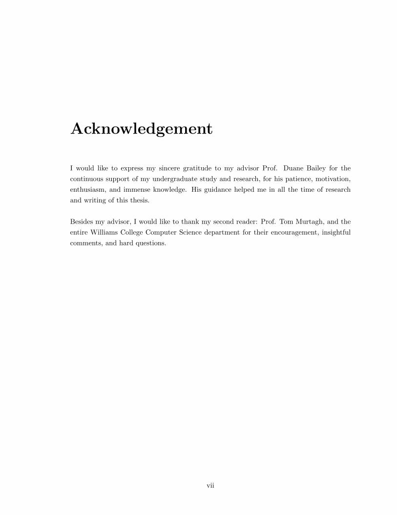
I would like to express my sincere gratitude to my advisor Prof. Duane Bailey for the
continuous support of my undergraduate study and research, for his patience, motivation,
enthusiasm, and immense knowledge. His guidance helped me in all the time of research
and writing of this thesis.
Besides my advisor, I would like to thank my second reader: Prof. Tom Murtagh, and the
entire Williams College Computer Science department for their encouragement, insightful
comments, and hard questions.
vii

Abstract
Roughly a decade ago, computing performance hit a power wall. With this came the power
consumption and heat dissipation concerns that have forced the semiconductor industry
to radically change its course, shifting focus from performance to power e�ciency. We
believe that Field programmable gate arrays (FPGAs) play an important role in this new
era. FPGAs combine the performance and power savings of specialized hardware while
maintaining the flexibility of general purpose processors (GPPs). Most importantly, pairing
an FPGAs with a GPP to support partnered computation can yield performance and energy
e�ciency improvements, and flexibility that neither device can achieve on their own. In this
work, we show that a GPP tightly coupled to a sequential vector processor implemented
on an FPGA, called Faux Vector Processor (FVP), can support e�cient, general purpose,
partnered computation.
viii

1. Introduction
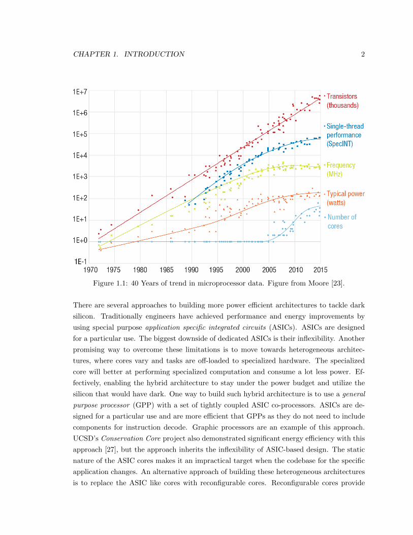
Microprocessor performance has increased dramatically over the past few decades. Until
recently, Gordon E. Moore’s famous observation that the number of transistors on integrated
circuits (IC
1) doubles roughly every 12-18 months (Moore’s law) has continued unabated.
The driving force behind Moore’s law is the continuous improvement of the complemen-
tary metal oxide semiconductor (CMOS) transistor technology, the basic building block of
digital electronic circuits. CMOS scaling has not only led to more transistors but also to
faster devices (shorter delay times and accordingly higher frequencies) that consume less
energy. During this period of growth, every generation of processor supported chips with
twice as many transistors, executing of about 40% faster and consuming roughly the same
total power as the previous generation [23]. The theory behind this technology scaling was
formulated by Dennard et al. [7] and is known as Dennard scaling. There was a time when
Dennard scaling accurately reflected what was happening in the semiconductor industry.
Unfortunately, those times have passed.
As the performance of processors improved due to shrinking transistors, the supply voltage
of the transistors was not dropping at the same rate. As a direct consequence, chip power
consumption grew with increased performance gains until only a decade ago. Higher power
consumption results from current leakage, producing more heat. Power consumption and
heat dissipation concerns have now forced the semiconductor industry to stop pushing clock
frequencies further, e↵ectively placing a tight limit on the total chip power. As a result,
the frequency scaling driven by shrinking transistors has hit the so-called power wall. This
trend is captured in Figure 1.1. In this new era, with each successive processor generation,
the percentage of a chip that can switch at full frequency is dropping exponentially due to
power constraints. Experiments conducted by Venkatesh et al. from UCSD show that we
can switch fewer than 7% of transistors on a chip at full frequency while remaining under a
power budget [27]. This percentage will decrease with each processor generation [27]. This
underutilization of transistors due to power consumption constraints is called dark silicon.
1A table of acronyms can be found beginning on page 68.
1
CHAPTER 1. INTRODUCTION 2
Figure 1.1: 40 Years of trend in microprocessor data. Figure from Moore [23].
There are several approaches to building more power e�cient architectures to tackle dark
silicon. Traditionally engineers have achieved performance and energy improvements by
using special purpose application specific integrated circuits (ASICs). ASICs are designed
for a particular use. The biggest downside of dedicated ASICs is their inflexibility. Another
promising way to overcome these limitations is to move towards heterogeneous architec-
tures, where cores vary and tasks are o↵-loaded to specialized hardware. The specialized
core will better at performing specialized computation and consume a lot less power. Ef-
fectively, enabling the hybrid architecture to stay under the power budget and utilize the
silicon that would have dark. One way to build such hybrid architecture is to use a general
purpose processor (GPP) with a set of tightly coupled ASIC co-processors. ASICs are de-
signed for a particular use and are more e�cient that GPPs as they do not need to include
components for instruction decode. Graphic processors are an example of this approach.
UCSD’s Conservation Core project also demonstrated significant energy e�ciency with this
approach [27], but the approach inherits the inflexibility of ASIC-based design. The static
nature of the ASIC cores makes it an impractical target when the codebase for the specific
application changes. An alternative approach of building these heterogeneous architectures
is to replace the ASIC like cores with reconfigurable cores. Reconfigurable cores provide
CHAPTER 1. INTRODUCTION 3
a compromise between GPPs and ASICs. Field Programmable Gate Arrays (FPGAs) are
ideal candidates for the reconfigurable cores. While FPGAs are generally less computa-
tionally powerful than GPPs, they are more flexible than ASICs. Therefore, FPGA-based
heterogeneous circuits consume moderate power, allow multiple specialized circuits to be
“loaded” whenever they are needed, drastically reduce time-to-market, and also provide
the ability to upgrade already deployed circuits. Of course, there is no free lunch: building
heterogeneous architectures with FPGAs is a di�cult and time-consuming process.
In this work, we explore the trade o↵s in designing a partnered computation pairing a GPP
with a FPGA based vector processor. Unlike a typical vector processor, our vector proces-
sor will be optimized towards power e�ciency rather than performance. Leading hardware
manufactures are also starting to realize the possibility of FPGA based co-processors [11].
Intel, leading chip manufacture, recently announced that it is working to produce a GPP
with a tightly coupled FPGA based processors. While FPGAs have made significant ad-
vances and are now highly capable, the software and documentation supporting them is still
primitive. Therefore, in this work we also use the vector processor as a target architecture
to take step closer towards mitigating the di�culties in programming FPGA to make it
more accessible to programmers.
The rest of the chapters are organized as follows. Chapter 2 goes over the previous work
on energy e�ciency; comparison between GPPs, ASICs, and FPGAs; FPGA-based vector
processors; heterogeneous co-processor systems; and power analysis on FPGA. Chapter 3
describes the traditional FPGA project workflow by walking through an example. In Chap-
ter 4, we present the design and goals of our FPGA-based faux vector processor (FVP),
followed by Chapter 5 that outlines our methodology for evaluating our design and describes
our results. Chapter 6 suggests some options for future exploration. Finally, Chapter 7
briefly summarizes our findings.
2. Previous Work
Previous research related to this work can be grouped into four main categories. First, there
is a large body of research focused on relative e�ciency of computation performed on GPPs,
FPGAs, and ASICs. Second, there has been significant work on improving the performance
of conventional vector processors and also on designs that include vector processors as co-
processors. Third, there have been a number of attempts to design performance enhancing
hardware designs. Finally, there is a small body of research focused on power analysis and
optimization on FPGAs. We consider these contributions in this section.
2.1 E�ciency Comparison Between GPPs, FPGAs, and ASICs
In this section, we’ll look at previous works focused on the e�ciency comparison between
GPPs, FPGAs, and ASICs that informed our research on the benefits of using FPGA based
cores.
Hill and Marty of University of Wisconsin extend Amdahl’s simple software model and
compute performance speedup for symmetric, asymmetric, and dynamic multicore chips
[13]. Amdahl’s software model is used to find the maximum expected improvement to an
overall system when only part of the system is improved. Symmetric processors dedicate the
same resources to each multicore (e.g. 16 identical 4-resource multicores on a 64-resource
chip), asymmetric processors have di↵erently sized cores (e.g. one 16-resource core and
24 2-resource cores), and dynamic processors can be run-time reconfigured to run as one
powerful core for sequential processing or as a set of possibly asymmetric smaller cores for
parallel processing. Even though multicore processors do not have application specific hard-
ware, asymmetric multicores represent a similar approach to that of ASICs: trying to break
up the larger computation into pieces that can be handled by optimally-sized sections of
hardware. Their key conclusion is that in terms of performance, the dynamic multicore de-
signs outperform asymmetric multicores, and asymmetric multicore designs perform better
than symmetric ones. Similar to Hill and Marty’s work, Woo and Lee of Georgia Institute
4
CHAPTER 2. PREVIOUS WORK 5
of Technology extend Amdahl’s law and develop analytcial power models for symmetric,
asymmetric, and dynamic chip design to evaluate energy e�ciency on the basis of power
models [29]. Their analysis demonstrates that symmetric and asymmetric multicore chips
can easily lose their energy e�ciency as the number of cores increases. Their work concludes
that a dynamic multicore processor with many small energy e�cient cores integrated with
a single larger core provides the best energy e�ciency.
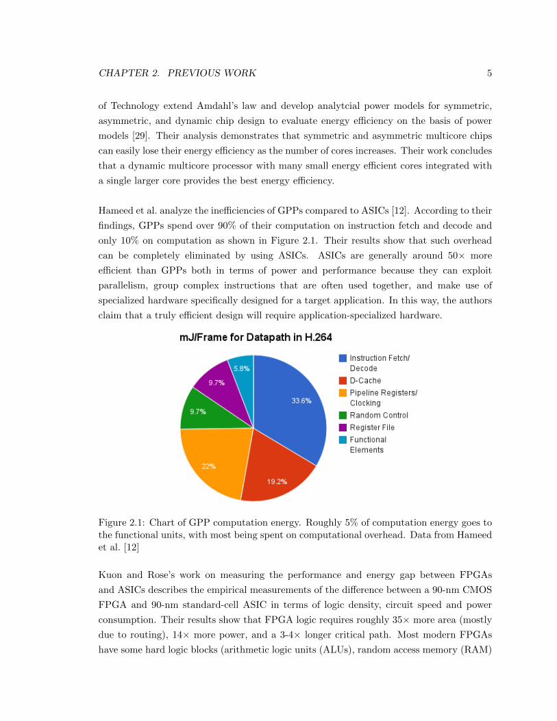
Hameed et al. analyze the ine�ciencies of GPPs compared to ASICs [12]. According to their
findings, GPPs spend over 90% of their computation on instruction fetch and decode and
only 10% on computation as shown in Figure 2.1. Their results show that such overhead
can be completely eliminated by using ASICs. ASICs are generally around 50⇥ more
e�cient than GPPs both in terms of power and performance because they can exploit
parallelism, group complex instructions that are often used together, and make use of
specialized hardware specifically designed for a target application. In this way, the authors
claim that a truly e�cient design will require application-specialized hardware.
Figure 2.1: Chart of GPP computation energy. Roughly 5% of computation energy goes to
the functional units, with most being spent on computational overhead. Data from Hameed
et al. [12]
Kuon and Rose’s work on measuring the performance and energy gap between FPGAs
and ASICs describes the empirical measurements of the di↵erence between a 90-nm CMOS
FPGA and 90-nm standard-cell ASIC in terms of logic density, circuit speed and power
consumption. Their results show that FPGA logic requires roughly 35⇥ more area (mostly
due to routing), 14⇥ more power, and a 3-4⇥ longer critical path. Most modern FPGAs
have some hard logic blocks (arithmetic logic units (ALUs), random access memory (RAM)
CHAPTER 2. PREVIOUS WORK 6
blocks, etc.), which can reduce those gaps to around 18⇥ for area, and 8⇥ for power with
only minor impact on the delay, depending on how much of the application hardware can
be mapped to those hard blocks. The cost of those improvements is the loss of flexibility
on the FPGA, as fabric space must be dedicated to the hard blocks, whether or not they
are used.
Chung et al. raise an interesting question in their work: “Does the future of chip design in-
clude custom logic, FPGAs, and General Purpose Graphic Processor Units (GPGPUs)?”[4].
They weigh the benefits and trade-o↵s associated with integrating unconventional cores (u-
cores) with GPPs to reach their conclusion that future chip design should include custom
logic. Since power consumption and I/O bandwidth are the two main performance bottle-
necks for modern computation, the authors evaluate three di↵erent types of u-cores, namely
ASICs, FPGAs, and GPGPUs, paired with GPPs in terms of energy e�ciency rather than
pure performance. To accurately measure the energy e�ciency, sequential operations are
performed on the GPP and parallel operations are performed on the u-cores. Their results
show that u-cores almost always improve the e�ciency of computation, especially as the
amount of parallelism in the target application increases. Further, the benefits of u-core
use are heavily dependent on o↵-chip bandwidth trends. This is because bandwidth ceilings
quickly become a limiting factor for extremely fast custom logic. Even if I/O and bandwidth
improvements continue to lag behind logic improvements, FPGAs will be able to o↵er per-
formance that is closer to that of ASICs than their relative computational e�ciency would
suggest. The authors conclude that ASICs o↵er both the highest performance and the most
power e�ciency, but that ASICs are expensive to develop and designed around a single set
of target applications. On the other hand, FPGAs can provide significant e�ciency gains
over GPPs alone while o↵ering more flexibility than ASICs.
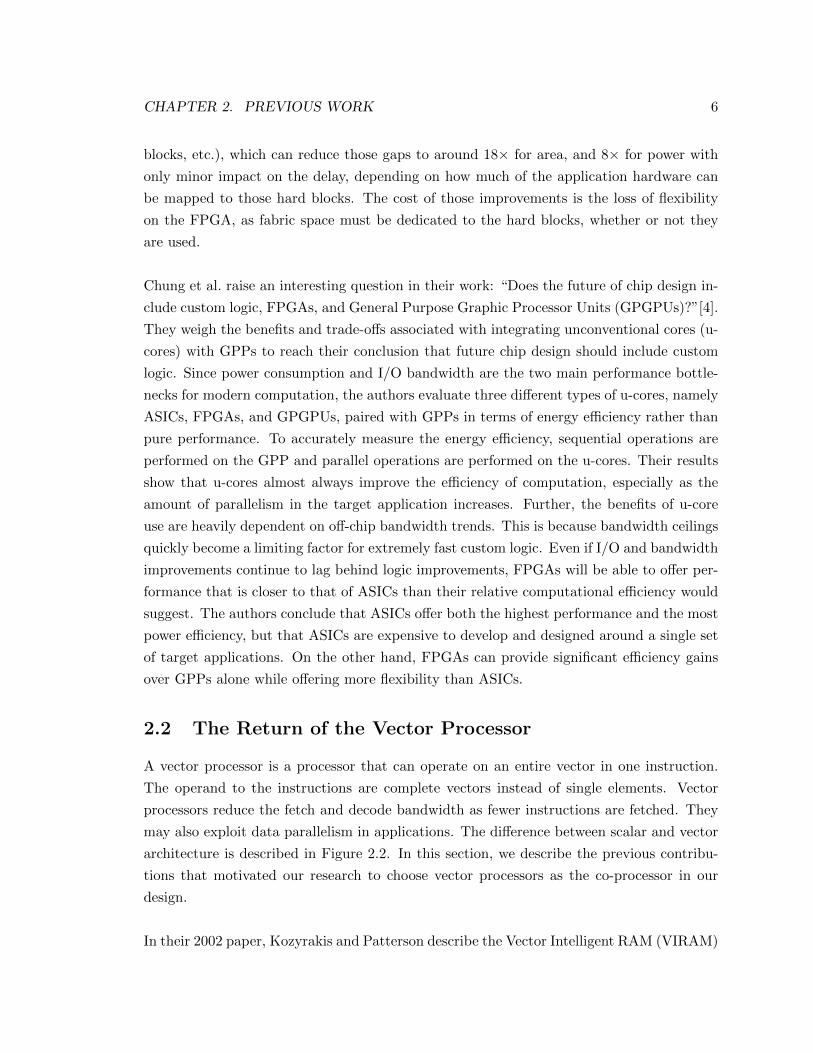
2.2 The Return of the Vector Processor
A vector processor is a processor that can operate on an entire vector in one instruction.
The operand to the instructions are complete vectors instead of single elements. Vector
processors reduce the fetch and decode bandwidth as fewer instructions are fetched. They
may also exploit data parallelism in applications. The di↵erence between scalar and vector
architecture is described in Figure 2.2. In this section, we describe the previous contribu-
tions that motivated our research to choose vector processors as the co-processor in our
design.
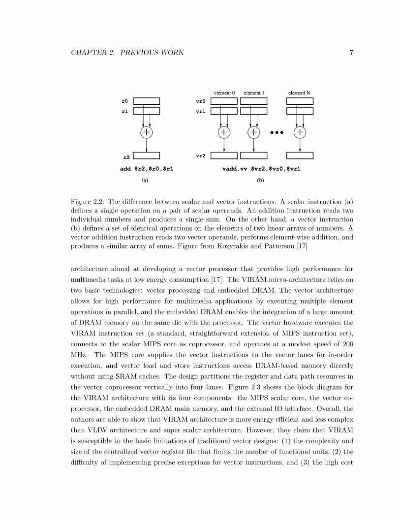
In their 2002 paper, Kozyrakis and Patterson describe the Vector Intelligent RAM (VIRAM)
CHAPTER 2. PREVIOUS WORK 7
Figure 2.2: The di↵erence between scalar and vector instructions. A scalar instruction (a)
defines a single operation on a pair of scalar operands. An addition instruction reads two
individual numbers and produces a single sum. On the other hand, a vector instruction
(b) defines a set of identical operations on the elements of two linear arrays of numbers. A
vector addition instruction reads two vector operands, performs element-wise addition, and
produces a similar array of sums. Figure from Kozyrakis and Patterson [17]
architecture aimed at developing a vector processor that provides high performance for
multimedia tasks at low energy consumption [17]. The VIRAM micro-architecture relies on
two basic technologies: vector processing and embedded DRAM. The vector architecture
allows for high performance for multimedia applications by executing multiple element
operations in parallel, and the embedded DRAM enables the integration of a large amount
of DRAM memory on the same die with the processor. The vector hardware executes the
VIRAM instruction set (a standard, straightforward extension of MIPS instruction set),
connects to the scalar MIPS core as coprocessor, and operates at a modest speed of 200
MHz. The MIPS core supplies the vector instructions to the vector lanes for in-order
execution, and vector load and store instructions access DRAM-based memory directly
without using SRAM caches. The design partitions the register and data path resources in
the vector coprocessor vertically into four lanes. Figure 2.3 shows the block diagram for
the VIRAM architecture with its four components: the MIPS scalar core, the vector co-
processor, the embedded DRAM main memory, and the external IO interface. Overall, the
authors are able to show that VIRAM architecture is more energy e�cient and less complex
than VLIW architecture and super scalar architecture. However, they claim that VIRAM
is susceptible to the basic limitations of traditional vector designs: (1) the complexity and
size of the centralized vector register file that limits the number of functional units, (2) the
di�culty of implementing precise exceptions for vector instructions, and (3) the high cost
CHAPTER 2. PREVIOUS WORK 8
of vector memory systems.
Figure 2.3: Figure showing the block diagram of VIRAM architecture. Figure from
Kozyrakis and Patterson [17]
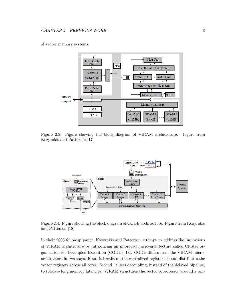
Figure 2.4: Figure showing the block diagram of CODE architecture. Figure from Kozyrakis
and Patterson [18]
In their 2003 followup paper, Kozyrakis and Patterson attempt to address the limitations
of VIRAM architecture by introducing an improved micro-architecture called Cluster or-
ganization for Decoupled Execution (CODE) [18]. CODE di↵ers from the VIRAM micro-
architecture in two ways. First, it breaks up the centralized register file and distributes the
vector registers across all cores. Second, it uses decoupling, instead of the delayed pipeline,
to tolerate long memory latencies. VIRAM structures the vector coprocessor around a cen-
CHAPTER 2. PREVIOUS WORK 9
tralized vector register file that provides operands to all functional units and connects them
to each other. In contrast, the composite approach organizes vector hardware as a collection
of interconnected cores. Each core is a simple vector processor with a set of local vector
registers and one functional unit. Each core can execute only a subset of the instruction
set. For example, one vector core may be able to execute all integer arithmetic instructions,
while another core handles vector load and store operations. The composite organization
breaks up the centralized vector register file into a distributed structure, and uses renam-
ing logic to map the vector registers defined in the VIRAM architecture to the distributed
register file. The composite organization uses a communication network for communication
and data exchange between vector cores, as there is no centralized register file to provide
the functionality of an all-to-all crossbar for vector operands. The block diagram of CODE
is shown in Figure 2.4. Their results show that CODE is 26% faster than a VIRAM with a
centralized vector register file that occupies approximately the same die area. They are also
able to show that CODE only su↵ers less than 5% performance loss due to precise excep-
tion support. Most importantly, CODE is able to scale the vector coprocessor in a flexible
manner by mixing the proper number and type of vector cores. If the typical workload for
a specific implementation includes a large number of integer operations, more vector cores
for integer instruction execution could be allocated. Similarly, if floating-point operations
are not necessary, all cores for floating-point instructions could be removed. In contrast,
with VIRAM one could only increase performance by allocating extra lanes, which evenly
scales integer and floating-point capabilities, regardless of the specific needs of applications.
Yu et al. demonstrate the potential for vector processing as a simple-to-use and salable ac-
celerator for soft processors [34]. Their architecture consists of a scalar core (single threaded
version of 32-bit Nios II), a vector processing unit, and a memory unit. The scalar core and
the vector unit share the same instruction memory and the same instruction fetch logic.
The scalar and vector units can execute instructions in parallel and also can coordinate via
a FIFO queue for instructions requiring both cores. The vector unit is a VIRAM based
vector architecture extended to take advantage of on chip memory blocks and hardware
multiply accumulate (MAC) units common in FPGAs. The vector unit is composed of
a specified number of vector lanes, each with complete copies of a functional unit, parti-
tion of the vector register file and vector flag registers, load store unit, and local memory.
Through performance modeling the authors are able to show that a vector processor can
potentially accelerate data parallel benchmarks with performance scaling better than Al-
tera’s behavioral synthesis tool even after manual code restructuring. Further, they are also
able to show how FPGA architectural features can be exploited to provide e�cient support
for some vector operations. For example, the multiply-accumulate blocks internally sum
multiple partial products from narrow multiplier circuits to implement wider multiplication
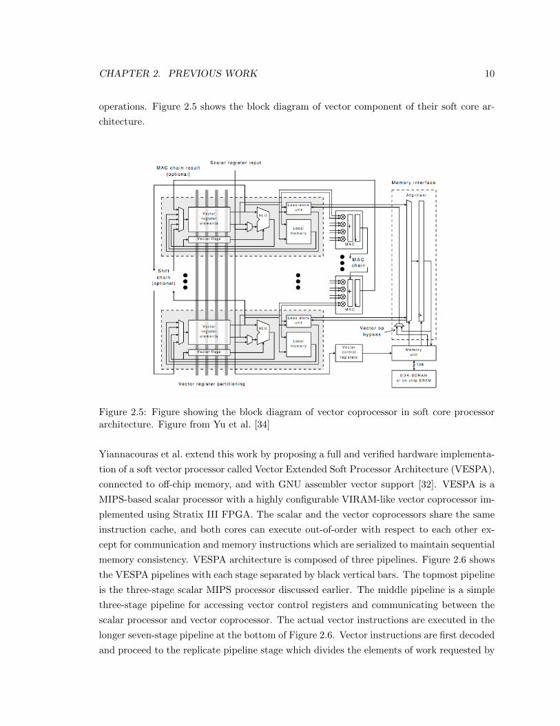
CHAPTER 2. PREVIOUS WORK 10
operations. Figure 2.5 shows the block diagram of vector component of their soft core ar-
chitecture.
Figure 2.5: Figure showing the block diagram of vector coprocessor in soft core processor
architecture. Figure from Yu et al. [34]
Yiannacouras et al. extend this work by proposing a full and verified hardware implementa-
tion of a soft vector processor called Vector Extended Soft Processor Architecture (VESPA),
connected to o↵-chip memory, and with GNU assembler vector support [32]. VESPA is a
MIPS-based scalar processor with a highly configurable VIRAM-like vector coprocessor im-
plemented using Stratix III FPGA. The scalar and the vector coprocessors share the same
instruction cache, and both cores can execute out-of-order with respect to each other ex-
cept for communication and memory instructions which are serialized to maintain sequential
memory consistency. VESPA architecture is composed of three pipelines. Figure 2.6 shows
the VESPA pipelines with each stage separated by black vertical bars. The topmost pipeline
is the three-stage scalar MIPS processor discussed earlier. The middle pipeline is a simple
three-stage pipeline for accessing vector control registers and communicating between the
scalar processor and vector coprocessor. The actual vector instructions are executed in the
longer seven-stage pipeline at the bottom of Figure 2.6. Vector instructions are first decoded
and proceed to the replicate pipeline stage which divides the elements of work requested by
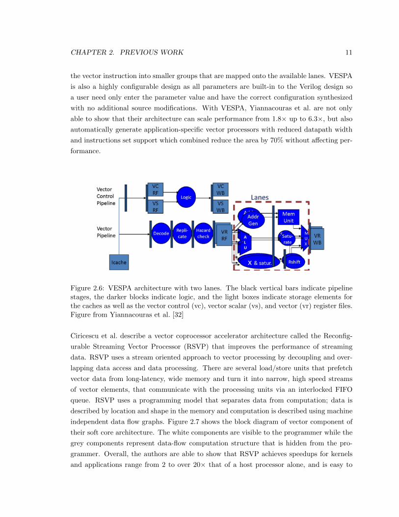
CHAPTER 2. PREVIOUS WORK 11
the vector instruction into smaller groups that are mapped onto the available lanes. VESPA
is also a highly configurable design as all parameters are built-in to the Verilog design so
a user need only enter the parameter value and have the correct configuration synthesized
with no additional source modifications. With VESPA, Yiannacouras et al. are not only
able to show that their architecture can scale performance from 1.8⇥ up to 6.3⇥, but alsoautomatically generate application-specific vector processors with reduced datapath width
and instructions set support which combined reduce the area by 70% without a↵ecting per-
formance.
Figure 2.6: VESPA architecture with two lanes. The black vertical bars indicate pipeline
stages, the darker blocks indicate logic, and the light boxes indicate storage elements for
the caches as well as the vector control (vc), vector scalar (vs), and vector (vr) register files.
Figure from Yiannacouras et al. [32]
Ciricescu et al. describe a vector coprocessor accelerator architecture called the Reconfig-
urable Streaming Vector Processor (RSVP) that improves the performance of streaming
data. RSVP uses a stream oriented approach to vector processing by decoupling and over-
lapping data access and data processing. There are several load/store units that prefetch
vector data from long-latency, wide memory and turn it into narrow, high speed streams
of vector elements, that communicate with the processing units via an interlocked FIFO
queue. RSVP uses a programming model that separates data from computation; data is
described by location and shape in the memory and computation is described using machine
independent data flow graphs. Figure 2.7 shows the block diagram of vector component of
their soft core architecture. The white components are visible to the programmer while the
grey components represent data-flow computation structure that is hidden from the pro-
grammer. Overall, the authors are able to show that RSVP achieves speedups for kernels
and applications range from 2 to over 20⇥ that of a host processor alone, and is easy to
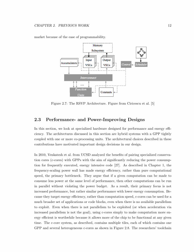
CHAPTER 2. PREVIOUS WORK 12
market because of the ease of programmability.
Figure 2.7: The RSVP Architecture. Figure from Ciricescu et al. [5]
2.3 Performance- and Power-Improving Designs
In this section, we look at specialized hardware designed for performance and energy e�-
ciency. The architectures discussed in this section are hybrid systems with a GPP tightly
coupled with one or more co-processing units. The architectural choices described in these
contributions have motivated important design decisions in our design.
In 2010, Venkatesh et al. from UCSD analyzed the benefits of pairing specialized conserva-
tion cores (c-cores) with GPPs with the aim of significantly reducing the power consump-
tion for frequently executed, energy intensive code [27]. As described in Chapter 1, the
frequency-scaling power wall has made energy e�ciency, rather than pure computational
speed, the primary bottleneck. They argue that if a given computation can be made to
consume less power at the same level of performance, then other computations can be run
in parallel without violating the power budget. As a result, their primary focus is not
increased performance, but rather similar performance with lower energy consumption. Be-
cause they target energy e�ciency, rather than computation speed, c-cores can be used for a
much broader set of applications or code blocks, even when there is no available parallelism
to exploit. Even when there is not parallelism to be exploited (or when acceleration via
increased parallelism is not the goal), using c-cores simply to make computation more en-
ergy e�cient is worthwhile because it allows more of the chip to be functional at any given
time. The c-core system, as described, contains multiple tiles, each of which contains one
GPP and several heterogeneous c-cores as shown in Figure 2.8. The researchers’ toolchain
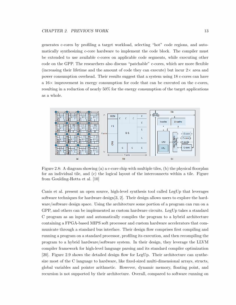
CHAPTER 2. PREVIOUS WORK 13
generates c-cores by profiling a target workload, selecting “hot” code regions, and auto-
matically synthesizing c-core hardware to implement the code block. The compiler must
be extended to use available c-cores on applicable code segments, while executing other
code on the GPP. The researchers also discuss “patchable” c-cores, which are more flexible
(increasing their lifetime and the amount of code they can execute) but incur 2⇥ area and
power consumption overhead. Their results suggest that a system using 18 c-cores can have
a 16⇥ improvement in energy consumption for code that can be executed on the c-cores,
resulting in a reduction of nearly 50% for the energy consumption of the target applications
as a whole.
Figure 2.8: A diagram showing (a) a c-core chip with multiple tiles, (b) the physical floorplan
for an individual tile, and (c) the logical layout of the interconnects within a tile. Figure
from Goulding-Hotta et al. [10]
Canis et al. present an open source, high-level synthesis tool called LegUp that leverages
software techniques for hardware design[3, 2]. Their design allows users to explore the hard-
ware/software design space. Using the architecture some portion of a program can run on a
GPP, and others can be implemented as custom hardware circuits. LegUp takes a standard
C program as an input and automatically compiles the program to a hybrid architecture
containing a FPGA-based MIPS soft processor and custom hardware accelerators that com-
municate through a standard bus interface. Their design flow comprises first compiling and
running a program on a standard processor, profiling its execution, and then recompiling the
program to a hybrid hardware/software system. In their design, they leverage the LLVM
compiler framework for high-level language parsing and its standard compiler optimization
[20]. Figure 2.9 shows the detailed design flow for LegUp. Their architecture can synthe-
size most of the C language to hardware, like fixed-sized multi-dimensional arrays, structs,
global variables and pointer arithmetic. However, dynamic memory, floating point, and
recursion is not supported by their architecture. Overall, compared to software running on
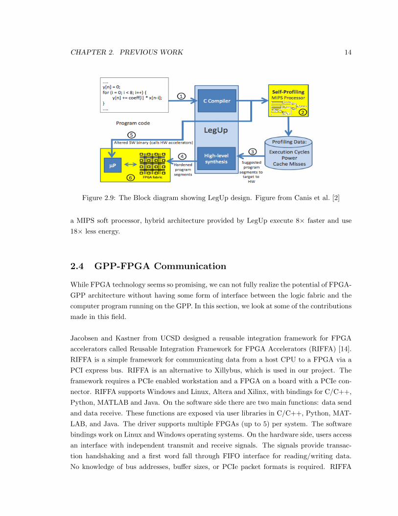
CHAPTER 2. PREVIOUS WORK 14
Figure 2.9: The Block diagram showing LegUp design. Figure from Canis et al. [2]
a MIPS soft processor, hybrid architecture provided by LegUp execute 8⇥ faster and use
18⇥ less energy.
2.4 GPP-FPGA Communication
While FPGA technology seems so promising, we can not fully realize the potential of FPGA-
GPP architecture without having some form of interface between the logic fabric and the
computer program running on the GPP. In this section, we look at some of the contributions
made in this field.
Jacobsen and Kastner from UCSD designed a reusable integration framework for FPGA
accelerators called Reusable Integration Framework for FPGA Accelerators (RIFFA) [14].
RIFFA is a simple framework for communicating data from a host CPU to a FPGA via a
PCI express bus. RIFFA is an alternative to Xillybus, which is used in our project. The
framework requires a PCIe enabled workstation and a FPGA on a board with a PCIe con-
nector. RIFFA supports Windows and Linux, Altera and Xilinx, with bindings for C/C++,
Python, MATLAB and Java. On the software side there are two main functions: data send
and data receive. These functions are exposed via user libraries in C/C++, Python, MAT-
LAB, and Java. The driver supports multiple FPGAs (up to 5) per system. The software
bindings work on Linux and Windows operating systems. On the hardware side, users access
an interface with independent transmit and receive signals. The signals provide transac-
tion handshaking and a first word fall through FIFO interface for reading/writing data.
No knowledge of bus addresses, bu↵er sizes, or PCIe packet formats is required. RIFFA
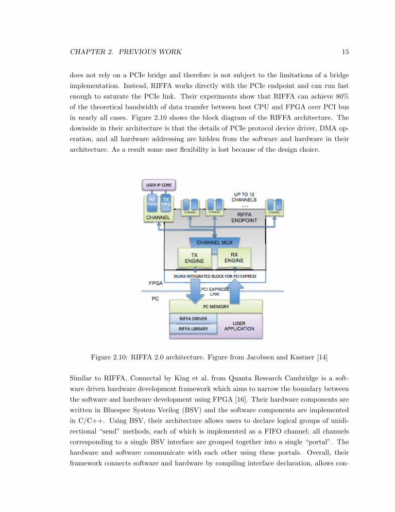
CHAPTER 2. PREVIOUS WORK 15
does not rely on a PCIe bridge and therefore is not subject to the limitations of a bridge
implementation. Instead, RIFFA works directly with the PCIe endpoint and can run fast
enough to saturate the PCIe link. Their experiments show that RIFFA can achieve 80%
of the theoretical bandwidth of data transfer between host CPU and FPGA over PCI bus
in nearly all cases. Figure 2.10 shows the block diagram of the RIFFA architecture. The
downside in their architecture is that the details of PCIe protocol device driver, DMA op-
eration, and all hardware addressing are hidden from the software and hardware in their
architecture. As a result some user flexibility is lost because of the design choice.
Figure 2.10: RIFFA 2.0 architecture. Figure from Jacobsen and Kastner [14]
Similar to RIFFA, Connectal by King et al. from Quanta Research Cambridge is a soft-
ware driven hardware development framework which aims to narrow the boundary between
the software and hardware development using FPGA [16]. Their hardware components are
written in Bluespec System Verilog (BSV) and the software components are implemented
in C/C++. Using BSV, their architecture allows users to declare logical groups of unidi-
rectional “send” methods, each of which is implemented as a FIFO channel; all channels
corresponding to a single BSV interface are grouped together into a single “portal”. The
hardware and software communicate with each other using these portals. Overall, their
framework connects software and hardware by compiling interface declaration, allows con-
CHAPTER 2. PREVIOUS WORK 16
current access to hardware accelerators from software, allows high-bandwidth sharing of
system memory with the hardware accelerators, and also provides portability across di↵er-
ent platforms.
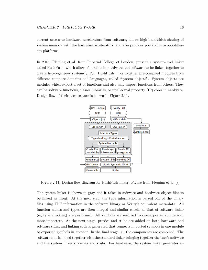
In 2015, Fleming et al. from Imperial College of London, present a system-level linker
called PushPush, which allows functions in hardware and software to be linked together to
create heterogeneous systems[8, 25]. PushPush links together pre-compiled modules from
di↵erent compute domains and languages, called “system objects”. System objects are
modules which export a set of functions and also may import functions from others. They
can be software functions, classes, libraries, or intellectual property (IP) cores in hardware.
Design flow of their architecture is shown in Figure 2.11.
Figure 2.11: Design flow diagram for PushPush linker. Figure from Fleming et al. [8]
The system linker is shown in gray and it takes in software and hardware object files to
be linked as input. At the next step, the type information is parsed out of the binary
files using ELF information in the software binary or Verity’s equivalent meta-data. All
function names and types are then merged and similar checks as that of software linker
(eg type checking) are performed. All symbols are resolved to one exporter and zero or
more importers. At the next stage, proxies and stubs are added on both hardware and
software sides, and linking code is generated that connects imported symbols in one module
to exported symbols in another. In the final stage, all the components are combined. The
software side is linked together with the standard linker bringing together the user’s software
and the system linker’s proxies and stubs. For hardware, the system linker generates an
CHAPTER 2. PREVIOUS WORK 17
IP block incorporating the CPU, user’s hardware, and the Advanced eXtensible Interface
(AXI) proxies and stubs. The final result is a single executable containing both software
and hardware. The researchers also built a fully functional and automated prototype on
the Zynq platform and are able to show that this type of linking enables a more equal
partnership between hardware and software, with hardware not just acting like a “dumb
accelerator” but also being able to initiate execution across the system.
2.5 Power Consumption Analysis on FPGA
Analysis and estimation for power dissipation of FPGAs has received little attention com-
pared to that of standard cell ASIC. Most of this limited research on FPGA power con-
sumption have focused primarily on dynamic power consumption. There has been very
little work to estimate and analyze static power consumption of FPGAs. In this section,
we discuss some of the work done towards analyzing both dynamic and static power con-
sumption on an FPGA. These contributions will serve as a reference for power analysis of
our design in later chapters.
Tuan and Lai from Xilinx Research Lab and UCLA analyze the leakage power of a low-cost
90nm FPGA using detailed device-level simulation. There simulations are performed using
DC operating point analysis in SPICE. DC operating point analysis calculates the behavior
of a circuit when a DC voltage or current is applied to it. The result of this analysis is
generally referred as the bias point, quiescent point or Q-point. The author’s measurement
methodology is based on measuring the power consumption by configurable logic blocks
(CLBs), building block of the FPGA circuit. The authors first divide the CLBs into smaller
circuit blocks. Next, each block is simulated individually to identify its leakage power con-
sumption. As the FPGA architecture is highly regular, iterating over all the circuit blocks
is quite manageable. The total leakage power of the CLB array is then computed by tak-
ing the sum of each block’s leakage power. Finally, this total power consumed by CLB
array is multiplied by the number of CLBs in the array to get the total leakage power.
To model the e↵ect of input variation, the simulation is performed under all possible in-
put states of circuit blocks. Using this methodology, they found that their FPGA consumes
4.2µW static power per CLB under normal conditions and more than 26µW per CLB in the
worst case. The authors conclude that there is a potential for substantial leakage reduction
through optimization of basic circuits and power management based on resource utilization.
Shang et al. from Princeton University and Xilinx Research Lab analyze the dynamic power
consumption in an FPGA by taking advantage of both simulation and measurement. The
CHAPTER 2. PREVIOUS WORK 18
target device for this project is a Xilinx Virtex-II. According to the authors, the total power
dissipation is a function of three factors. First is the e↵ective capacitance, which is defined
as the “parasitic” e↵ect due to interconnection wires and transistors, and the emulated
capacitance because of short-circuit current. The e↵ective capicatance of each resource
is computed using direct measurement and SPICE simulation. The second factor is the
resource utilization, i.e the proportion of look up tables (LUTs), block RAMs (BRAMs) etc
used in circuit design. Finally, the most important factor determining the power dissipation
is the switching activity. Switching activity is defined as the number of signal transitions
in a clock period. Resource utilization and switching activity is computed using software
called Modelsim. The authors model these factors as follows
P =
1
2
V
2f
X
i
CiUiSi
where V is the supply voltage, f is the operating frequency, and Ci, Ui, Si are the e↵ective
capacitance, utilization, and switching activity of each resource, respectively. Using this
equation, the authors compute the power dissipation of few benchmark circuits. According
to their results most of the power dissipation occurs in the interconnection resources. The
authors also conclude that for the xilinx Vertex-II FPGA operating at 100MHz with input
voltage of 1.5V, each CLB would consume 5.9µW per MHz.
There has been considerable work on dynamic power analysis on FPGAs. Degalahal and
Tuan model dynamic power consumption of FPGA based on clock power, switching activity,
and dominant interconnect capacitance. Similarly, Jevtic and Carreras present a measure-
ment model that separately measures clock, interconnect, and logic power to compute the
total dynamic power consumed by the FPGA. These are some direct ways of measuring
power consumption on an FPGA. An alternative to this approach is to rely on power anal-
ysis software to measure the power consumption. For the purpose of this project, we relied
on Vivado’s power analysis tool to measure the power consumption of our design, and are
aware that better estimates are possible.
2.6 Summary
The computational performance of a chip has hit a power wall [27]. As a result, it is
becoming increasingly di�cult to improve energy e�ciency while maintaining computa-
tional performance. A lot of work has been done to evaluate the performance and energy
e�ciency of ASICs, FPGAs, and GPPs to determine the right architecture for the job.
The past works comparing di↵erent kinds of heterogeneous processors have shown that
CHAPTER 2. PREVIOUS WORK 19
even though ASICs have a considerable performance advantage compared to FPGAs, FP-
GAs can be significantly more e�cient than general purpose processors while maintaining
enough flexibility to be used for a wide variety of applications. Furthermore, designs that
combine heterogeneous accelerators with GPPs make it clear that such a design can o↵er
significant flexiblity with performance and e�ciency gains compared to a GPP, ASIC, or
FPGA alone. The c-core and QS-core research [27, 28] suggests that a system integrat-
ing automatically generated ASICs with a modified compiler and runtime controller can
significantly reduce power consumption. Similarly, the RIFFA, PushPush, and Connectal
research [3, 8, 16] have shown that a system integrating FPGA with a modified runtime
controller can significantly improve power and performance e�ciency. These e↵orts have
focused on trading execution of instruction for hardware, and mostly neglect the possibility
to harness the power of parallelism. Previous works on vector processors have shown the
possibility to solve the problem through parallelism. The projects like VIRAM, VESPA,
CODE, RSVP [17, 18, 32, 5] have made it clear that vectors processors can be very e�cient
co-processors and can provide significant performance and energy boost. Works described
in this section suggests that a heterogeneous design with a GPP tightly coupled with one
or many reconfigurable co-processors would yield significant energy e�ciency gains while
maintaining flexibility.
3. The FPGA Work Flow
Since FPGAs provide a compromise between the performance of ASICs and the flexibility
of GPPs, the FPGA seems an ideal partner for a GPP. The Xilinx Zynq-7000 is one such
heterogeneous computing platform used in this project. It integrates a dual-core Cortex
A9 ARM processor and an FPGA inside one chip. Moreover, because of its tightly-coupled
processing system (PS) and programmable logic (PL), the Xilinx’s Zynq seems to be an
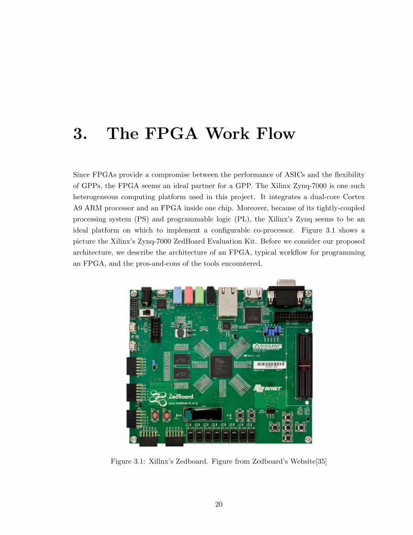
ideal platform on which to implement a configurable co-processor. Figure 3.1 shows a
picture the Xilinx’s Zynq-7000 ZedBoard Evaluation Kit. Before we consider our proposed
architecture, we describe the architecture of an FPGA, typical workflow for programming
an FPGA, and the pros-and-cons of the tools encountered.
Figure 3.1: Xillnx’s Zedboard. Figure from Zedboard’s Website[35]
20
CHAPTER 3. THE FPGA WORK FLOW 21
3.1 Field Programmable Gate Array Architecture
In this section, we give an overview of the technology behind field programmable gate arrays
(FPGAs). FPGAs arose from programmable logic devices (PLDs), which first appeared in
early 1970s. However, these early FPGAs were very limited as programmable logic was
hardwired between logic gates. In 1985, the first commercially available FPGA (the Xilinx
XC2064) hosted arrays of configurable logic blocks (CLBs) that contained programmable
gates as well as programmable interconnect between the CLBs. Since then FPGAs have
rapidly evolved.
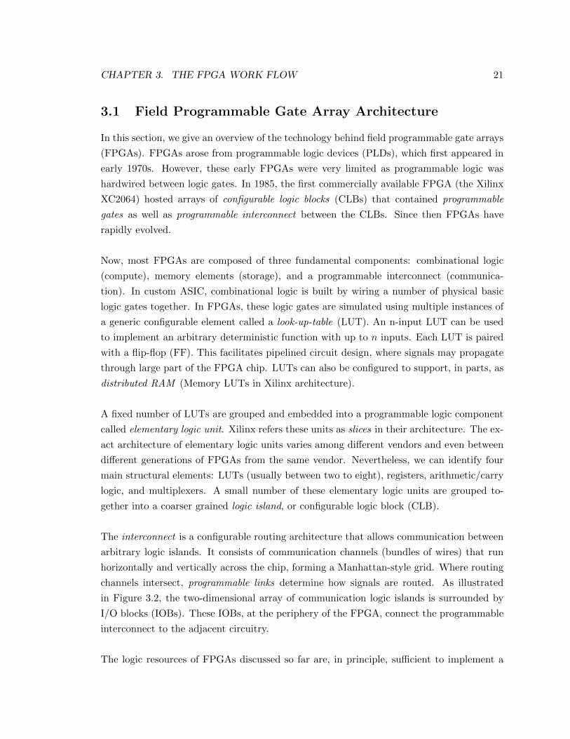
Now, most FPGAs are composed of three fundamental components: combinational logic
(compute), memory elements (storage), and a programmable interconnect (communica-
tion). In custom ASIC, combinational logic is built by wiring a number of physical basic
logic gates together. In FPGAs, these logic gates are simulated using multiple instances of
a generic configurable element called a look-up-table (LUT). An n-input LUT can be used
to implement an arbitrary deterministic function with up to n inputs. Each LUT is paired
with a flip-flop (FF). This facilitates pipelined circuit design, where signals may propagate
through large part of the FPGA chip. LUTs can also be configured to support, in parts, as
distributed RAM (Memory LUTs in Xilinx architecture).
A fixed number of LUTs are grouped and embedded into a programmable logic component
called elementary logic unit. Xilinx refers these units as slices in their architecture. The ex-
act architecture of elementary logic units varies among di↵erent vendors and even between
di↵erent generations of FPGAs from the same vendor. Nevertheless, we can identify four
main structural elements: LUTs (usually between two to eight), registers, arithmetic/carry
logic, and multiplexers. A small number of these elementary logic units are grouped to-
gether into a coarser grained logic island, or configurable logic block (CLB).
The interconnect is a configurable routing architecture that allows communication between
arbitrary logic islands. It consists of communication channels (bundles of wires) that run
horizontally and vertically across the chip, forming a Manhattan-style grid. Where routing
channels intersect, programmable links determine how signals are routed. As illustrated
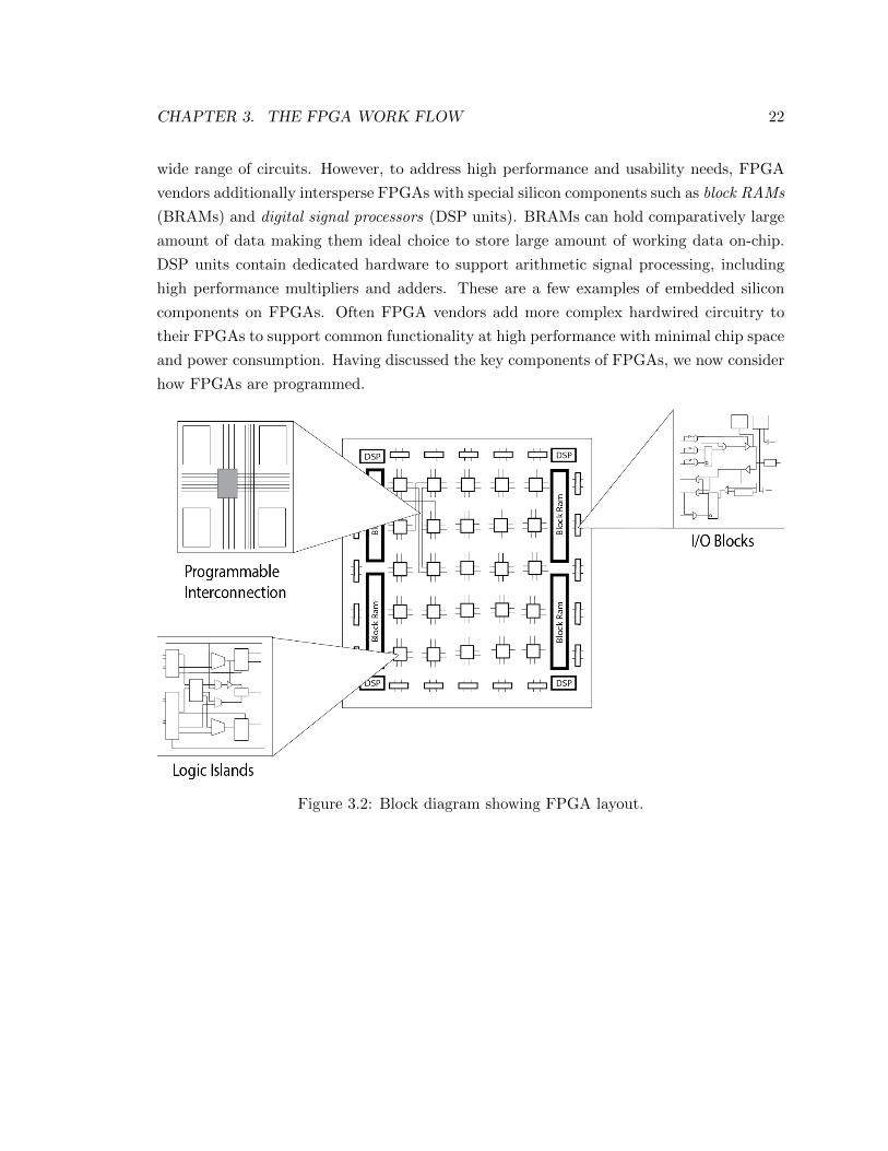
in Figure 3.2, the two-dimensional array of communication logic islands is surrounded by
I/O blocks (IOBs). These IOBs, at the periphery of the FPGA, connect the programmable
interconnect to the adjacent circuitry.
The logic resources of FPGAs discussed so far are, in principle, su�cient to implement a
CHAPTER 3. THE FPGA WORK FLOW 22
wide range of circuits. However, to address high performance and usability needs, FPGA
vendors additionally intersperse FPGAs with special silicon components such as block RAMs
(BRAMs) and digital signal processors (DSP units). BRAMs can hold comparatively large
amount of data making them ideal choice to store large amount of working data on-chip.
DSP units contain dedicated hardware to support arithmetic signal processing, including
high performance multipliers and adders. These are a few examples of embedded silicon
components on FPGAs. Often FPGA vendors add more complex hardwired circuitry to
their FPGAs to support common functionality at high performance with minimal chip space
and power consumption. Having discussed the key components of FPGAs, we now consider
how FPGAs are programmed.
Figure 3.2: Block diagram showing FPGA layout.
CHAPTER 3. THE FPGA WORK FLOW 23
3.2 Architecture Supporting Partnered Communication
One of the daunting tasks in FPGA design is e↵ectively communicate with adjacent pro-
cessors. Implementing the low-level bus protocols is a project in itself. In this work, we
used a pre-packaged communication solution, Xillybus, to allow us to focus our e↵orts on
co-processor design.
Xillybus consists of an IP core and a Linux driver. IP cores are the FPGA equivalent of
library functions. IP cores may implement certain mathematical functions, a functional
unit (example, a USB interface), an entire processor (e.g. ARM). They promote hardware
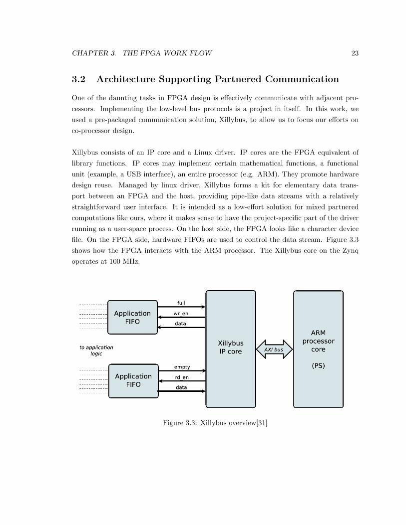
design reuse. Managed by linux driver, Xillybus forms a kit for elementary data trans-
port between an FPGA and the host, providing pipe-like data streams with a relatively
straightforward user interface. It is intended as a low-e↵ort solution for mixed partnered
computations like ours, where it makes sense to have the project-specific part of the driver
running as a user-space process. On the host side, the FPGA looks like a character device
file. On the FPGA side, hardware FIFOs are used to control the data stream. Figure 3.3
shows how the FPGA interacts with the ARM processor. The Xillybus core on the Zynq
operates at 100 MHz.
Figure 3.3: Xillybus overview[31]
CHAPTER 3. THE FPGA WORK FLOW 24
3.3 FPGA reconfiguration workflow
To demonstrate the considerations encountered in the typical FPGA workflow, we walk
through the implementation of a typical application: computation of the dot product of
two vectors.
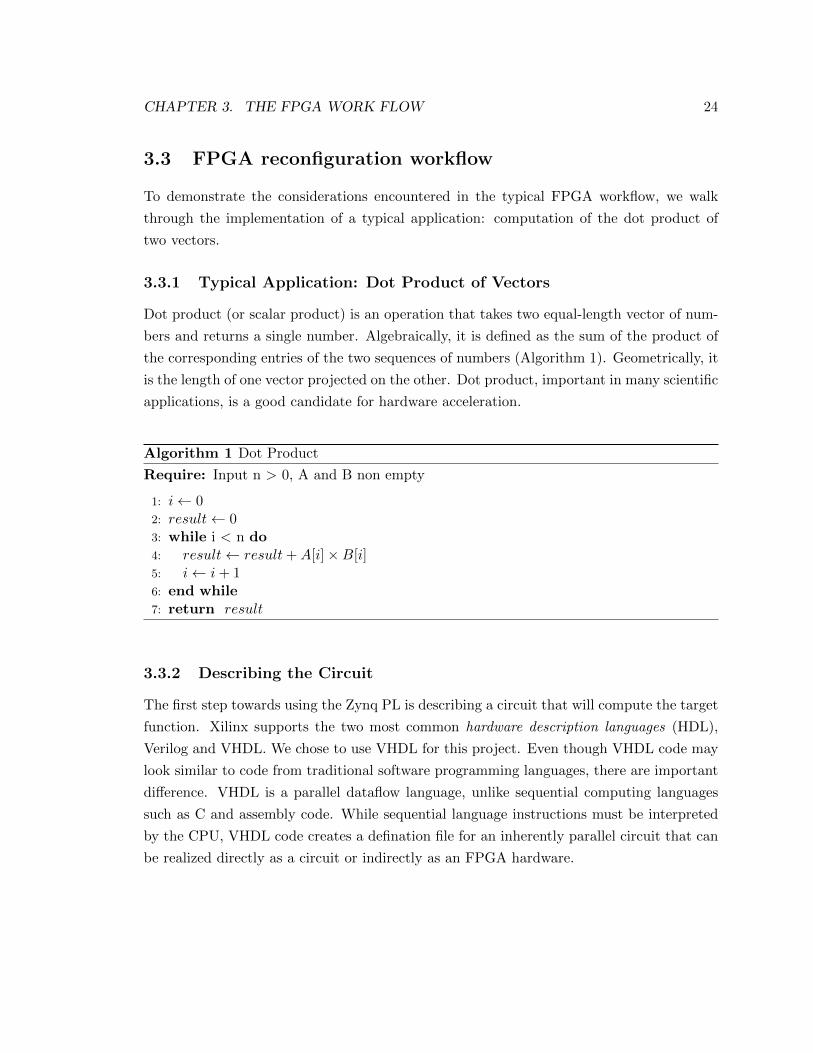
3.3.1 Typical Application: Dot Product of Vectors
Dot product (or scalar product) is an operation that takes two equal-length vector of num-
bers and returns a single number. Algebraically, it is defined as the sum of the product of
the corresponding entries of the two sequences of numbers (Algorithm 1). Geometrically, it
is the length of one vector projected on the other. Dot product, important in many scientific
applications, is a good candidate for hardware acceleration.
Algorithm 1 Dot Product
Require: Input n > 0, A and B non empty
1: i 0
2: result 0
3: while i < n do4: result result+A[i]⇥B[i]
5: i i+ 1
6: end while7: return result
3.3.2 Describing the Circuit
The first step towards using the Zynq PL is describing a circuit that will compute the target
function. Xilinx supports the two most common hardware description languages (HDL),
Verilog and VHDL. We chose to use VHDL for this project. Even though VHDL code may
look similar to code from traditional software programming languages, there are important
di↵erence. VHDL is a parallel dataflow language, unlike sequential computing languages
such as C and assembly code. While sequential language instructions must be interpreted
by the CPU, VHDL code creates a defination file for an inherently parallel circuit that can
be realized directly as a circuit or indirectly as an FPGA hardware.
CHAPTER 3. THE FPGA WORK FLOW 25
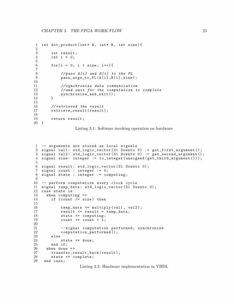
1 int dot_product(int* A, int* B, int size){2
3 int result;4 int i = 0;5
6 for(i = 0; i < size; i++){7
8 //pass A[i] and B[i] to the PL
9 pass_args_to_PL(A[i],B[i],size);10
11 // synchronize data communication
12 //and wait for the computation to complete
13 synchronize_and_wait ();14 }15
16 // retrieved the result
17 retrieve_result(result);18
19 return result;20 }
Listing 3.1: Software invoking operation on hardware
1 -- arguments are stored as local signals2 signal val1: std_logic_vector (31 Downto 0) := get_first_argument ();3 signal val2: std_logic_vector (31 Downto 0) := get_second_argument ();4 signal size: integer := to_integer(unsigned(get_third_argument ()));5
6 signal result: std_logic_vector (31 Downto 0);7 signal count : integer := 0;8 signal state : integer := computing;9
10 -- perform computation every clock cycle11 signal temp_data: std_logic_vector (31 Downto 0);12 case state is13 when computing =>14 if (count /= size) then15
16 temp_data <= multiply(val1 , val2);17 result <= result + temp_data;18 state <= computing;19 count <= count + 1;20
21 --signal computation performed; synchronize22 computation_performed ();23 else24 state <= done;25 end if;26 when done =>27 transfer_result_back(result);28 state <= complete;29 end case;
Listing 3.2: Hardware implementation in VHDL
CHAPTER 3. THE FPGA WORK FLOW 26
To show how to perform dot product of vectors using this software-hardware hybrid ar-
chitecture, we implemented Algorithm 1 in C and VHDL. These two implementations are
shown in Listings 3.1 and 3.2, respectively.
The computation is initiated in the processing system (PS), with software passing required
values to the hardware. The software then waits. Once the programmable logic (PL) gets
the required values, the computation starts. Computation happens every clock cycle. Since
the clocks are running at di↵erent speed on PS and PL, two computing partners must be
synchronized. This process repeats until all the entries of the vectors have been consumed.
The PL then sends the result back to the software, and the computation is complete.
3.3.3 Simulation
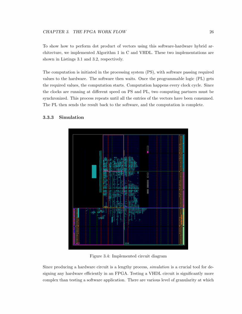
Figure 3.4: Implemented circuit diagram
Since producing a hardware circuit is a lengthy process, simulation is a crucial tool for de-
signing any hardware e�ciently in an FPGA. Testing a VHDL circuit is significantly more
complex than testing a software application. There are various level of granularity at which
CHAPTER 3. THE FPGA WORK FLOW 27
a circuit can be simulated (eg, high level behavioral correctness to estimating propagation
delays) and a VHDL testbench created for simulation must accurately mimic the hardware
environment. Instead of simply calling a function with few di↵erent test inputs, a designer
must define and provide a clocking mechanism and interfaces between the circuit being
tested and the testing unit.
The next step is inserting any new intellectual property (IP) blocks. To use the newly cre-
ated IP core, it must be interconnected with other hardware, which e↵ectively lays out a
floor plan. This involves importing other Xilinx IPs, including the IP for the ARM PS, and
connecting the di↵erent pieces of IP correctly.
3.3.4 Synthesis and Implementation
Once the block diagram is complete and all interconnects have been managed correctly, it
is synthesized and implemented. Unlike software compilation, which usually takes a few
seconds, Vivado’s synthesis generally take a few minutes to run. This makes turnaround
time to updating an IP core extremely time consuming, as even minor changes require
a significant amount of time to implement. Synthesis and implementation output many
reports, some of which detail the resource utilization of the IP cores, and predicted power
consumption by the implemented circuit. A picture of hardware implementation of the
design is shown in Figure 3.4. Finally, bitstream is generated for the implemented design.
The bitstream file augments the system boot file and is loaded by the first stage boot loader
to initialize the FPGA before the processor is booted. Once installed, the hardware is
available through Xillybus device file.
3.4 Summary
Even though Zynq is a great system to build a tightly-coupled coprocessor for a GPP, the
process of programing the system is very much involved. We believe that complexity of this
process represents a significant “barrier-to-entry” for new applications. This is unfortunate,
given the great potential of these systems. In the next chapter, we describe an IP core that,
at a high level, can be reconfigured or reprogrammed very easily. We believe this approach
of targeting a reconfigurable one-time-programmed co-processor represents a happy medium
between dedicated ASIC design and user-driven FPGA design as it combines the flexibility
and e�ciency of both.
4. Faux-Vector Processor
In-spite of the complex programming model, the concept and benefits of an FPGA-based
co-processor is very promising as it combines favourable characteristics of GPP and ASIC
designs. In this section, we propose a FPGA-based vector reconfigurable co-processor.
Along with the design and implementation details of the co-processor, we also provide some
example applications that make use of the co-processor.
Previous research suggests that FPGA-based co-processors can provide significant perfor-
mance improvement over a GPP alone. However, FPGA flexibility and e�ciency comes at
a significant workflow-cost. The devices are complex (Zynq’s 1863 page manual [30]); the
learning curve for VHDL is steep; and the configuration tool is buggy and poorly docu-
mented. Still, FPGAs remain popular devices supporting soft processors used in embedded
systems. Soft processors are HDL-specified processors that can be configured in various
ways supporting varying performance and resource utilization. The key benefit of using
FPGAs for soft processors is that they can achieve high performance with reduced devel-
opment e↵ort to the user once they are designed. As a primary goal to this work, we have
designed a soft vector processor called the Faux-Vector Processor (FVP).
In this new power-conscious era, e↵orts like the Conservation Core project from UCSD [27]
have demonstrated a new way of designing power-e�cient chips by configuring the excess
transistors on the chip as power e�cient hardware for specific application. In this work,
we replace ASIC-like static core with a FPGA-based reconfigurable core, the FVP. This
vector processor is optimized for power e�ciency rather than speed. In a traditional GPP,
a significant percent of power consumption comes from interpreting instructions. Vector
processors perform entire loops as a single instruction so they can significantly reduce the
power associated with instruction interpretation. We leverage this aspect of vector processor
design to implement a single lane vector processor to realize the potential of performing
computation with less overall power. The single lane vector processor executes operations
sequentially rather than in parallel, hence the name Faux Vector Processor.
28
CHAPTER 4. FAUX-VECTOR PROCESSOR 29
4.1 FVP Architectural Overview
The FVP is a single-instruction-multiple-data (SIMD) array of virtual processors (VPs) em-
bedded on a Zynq processor. The number of VPs is the same as the vector length (VL). All
VPs execute the same operation specified by a single vector instruction. The instruction set
in this architecture borrows heavily from the VIRAM instruction set [21], which is designed
as a vector extension to the MIPS-IV instruction set. A few instructions are borrowed from
VESPA’s ISA [33]. Operations however are performed sequentially rather than in parallel;
the processor’s focus is the development of power-e�ciency without reduction of perfor-
mance.
4.1.1 Interface
NLane and MVL are fixed for the processor. They control the number of parallel vector lanes
and functional units that are logically available in the processor, and the maximum length
of the vectors that can be stored in the processor’s vector register file, respectively. VPW
and MemMinWidth control the data width of the VPs, and the minimum data width that
can be accessed by vector memory instructions, respectively. Table 4.1 shows the list of
parameters for the processor, their descriptions, and possible values.
Table 4.1: List of parameters for the Faux Vector Processor
Parameter Description Range of values Type
NLane Number of lanes 1 Fixed
MVL Maxumum vector length 64 Fixed
VPW Processor data width (in bits) 8,16,32 Variable
VL Vector Length 1-64 Variable
MemWidth Memory interface width (bits) 32,64 Variable
MemMinWidth Minimum accessible data width in memory 8,16,32 Variable
The architecture defines sixty-four vector registers, and thirty-two 32-bit scalar registers.
Vector-scalar instructions and certain memory operations require vector register and scalar
register operands. Scalar register values can be transferred to and from vector registers or
vector control registers using the vext, vins, vmstc, vmcts instructions.
Further, the architecture defines thirty-two vector flag registers. The flag registers are writ-
ten to by comparison instructions and are operated on by flag logical instructions. The
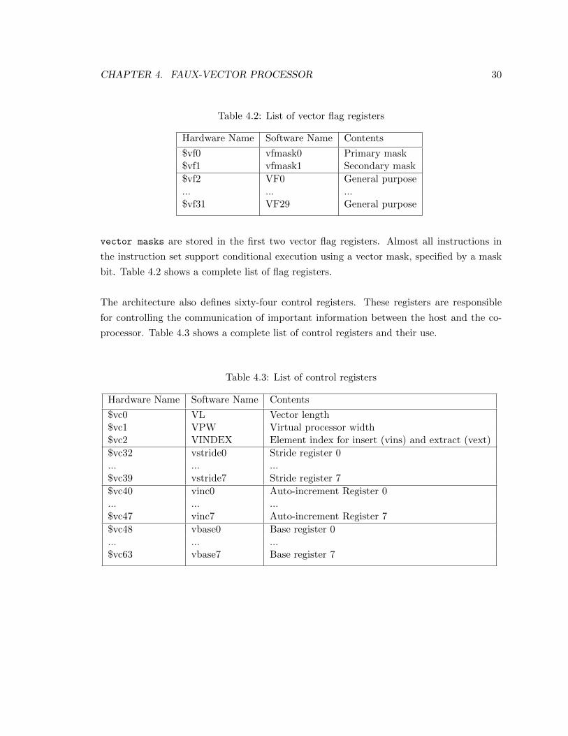
CHAPTER 4. FAUX-VECTOR PROCESSOR 30
Table 4.2: List of vector flag registers
Hardware Name Software Name Contents
$vf0 vfmask0 Primary mask
$vf1 vfmask1 Secondary mask
$vf2 VF0 General purpose
... ... ...
$vf31 VF29 General purpose
vector masks are stored in the first two vector flag registers. Almost all instructions in
the instruction set support conditional execution using a vector mask, specified by a mask
bit. Table 4.2 shows a complete list of flag registers.
The architecture also defines sixty-four control registers. These registers are responsible
for controlling the communication of important information between the host and the co-
processor. Table 4.3 shows a complete list of control registers and their use.
Table 4.3: List of control registers
Hardware Name Software Name Contents
$vc0 VL Vector length
$vc1 VPW Virtual processor width
$vc2 VINDEX Element index for insert (vins) and extract (vext)
$vc32 vstride0 Stride register 0
... ... ...
$vc39 vstride7 Stride register 7
$vc40 vinc0 Auto-increment Register 0
... ... ...
$vc47 vinc7 Auto-increment Register 7
$vc48 vbase0 Base register 0
... ... ...
$vc63 vbase7 Base register 7
CHAPTER 4. FAUX-VECTOR PROCESSOR 31
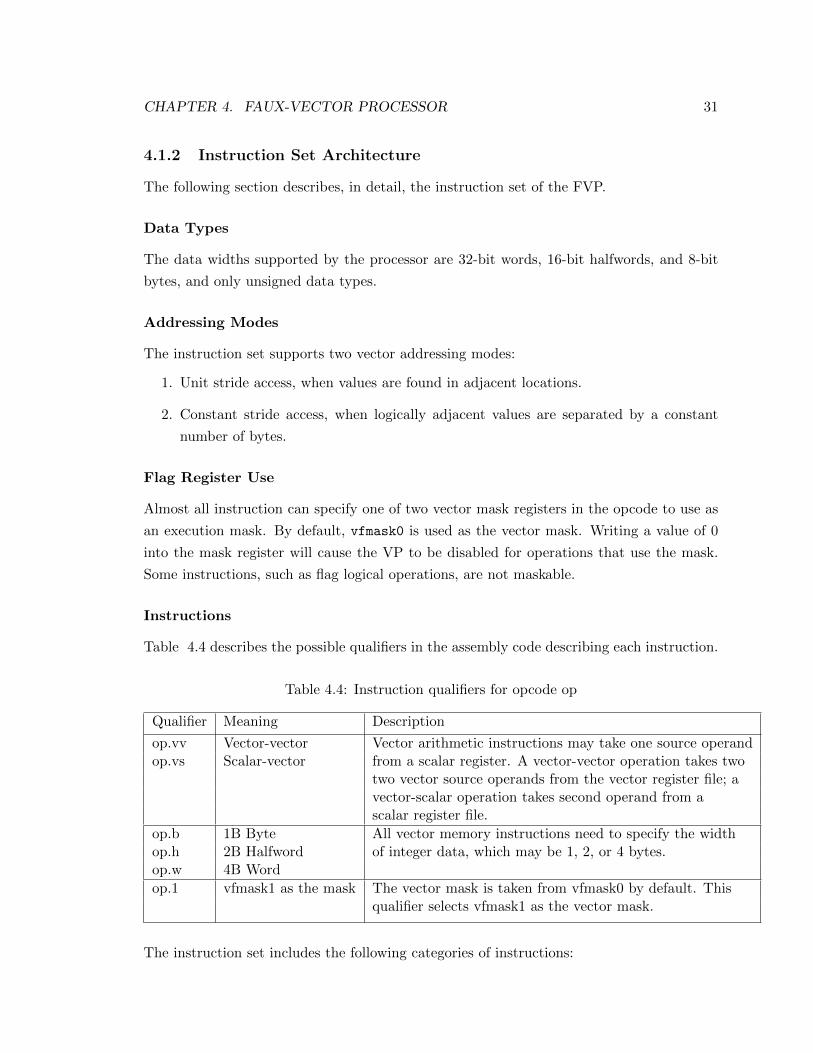
4.1.2 Instruction Set Architecture
The following section describes, in detail, the instruction set of the FVP.
Data Types
The data widths supported by the processor are 32-bit words, 16-bit halfwords, and 8-bit
bytes, and only unsigned data types.
Addressing Modes
The instruction set supports two vector addressing modes:
1. Unit stride access, when values are found in adjacent locations.
2. Constant stride access, when logically adjacent values are separated by a constant
number of bytes.
Flag Register Use
Almost all instruction can specify one of two vector mask registers in the opcode to use as
an execution mask. By default, vfmask0 is used as the vector mask. Writing a value of 0
into the mask register will cause the VP to be disabled for operations that use the mask.
Some instructions, such as flag logical operations, are not maskable.
Instructions
Table 4.4 describes the possible qualifiers in the assembly code describing each instruction.
Table 4.4: Instruction qualifiers for opcode op
Qualifier Meaning Description
op.vv Vector-vector Vector arithmetic instructions may take one source operand
op.vs Scalar-vector from a scalar register. A vector-vector operation takes two
two vector source operands from the vector register file; a
vector-scalar operation takes second operand from a
scalar register file.
op.b 1B Byte All vector memory instructions need to specify the width
op.h 2B Halfword of integer data, which may be 1, 2, or 4 bytes.
op.w 4B Word
op.1 vfmask1 as the mask The vector mask is taken from vfmask0 by default. This
qualifier selects vfmask1 as the vector mask.
The instruction set includes the following categories of instructions:
CHAPTER 4. FAUX-VECTOR PROCESSOR 32
1. Vector Arithmetic Instructions, for arithmetic operations on vectors.
2. Vector Logical Instructions, for comparison of vectors.
3. Vector Flag Processing Instructions, for explicitly loading and storing mask values.
4. Vector Processing Instructions
5. Memory instructions, for loading and storing vectors.
Table 4.5: Vector arithmetic instructions
Name Mnemonic Syntax Summary
Absolute Value vabs .vv[.1] vD, vA Each unmasked VP writes into vD the
absolute value of vA.
Add vadd .vv[.1] vD, vA, vB Each unmasked VP writes into vD the
.vs[.1] vD, vA, rS unsigned integer sum of vA and vB or rS.
Subtract vsub .vv[.1] vD, vA, vB Each unmasked VP writes into vD the
.vs[.1] vD, vA, rS unsigned integer result of vA minus vB or rS.
Multiply Low mult .vv[.1] vD, vA, vB Each unmasked VP writes into vD the
.vs[.1] vD, vA, rS lower half of unsigned integer result of
vA times vB or rS.
Shift vsra .vv[.1] vD, vA, vB Each unmasked VP writes into vD the
Right .vs[.1] vD, vA, rS result of logical right shifting
Logical vA by vB or rS.
Shift vsrl .vv[.1] vD, vA, vB Each unmasked VP writes into vD the
Left .vs[.1] vD, vA, rS result of logical left shifting
Logical vA by vB or rS.
Minimum vmin .vv[.1] vD, vA, vB Each unmasked VP writes into vD the
.vs[.1] vD, vA, rS minimum of vA and vB or rS.
Maximum vmax .vv[.1] vD, vA, vB Each unmasked VP writes into vD the
.vs[.1] vD, vA, rS maximum of vA and vB or rS.
Compare Less Than vcmplt .vv[.1] vF, vA, vB Each unmasked VP writes into vF the
Compare Less than Equal vcmplte .vs[.1] vF, vA, rS boolean result of comparing vA and vB or rS.
Compare Equal vcmpe .vv[.1] vF, vA, vB Each unmasked VP writes into vF the
Compare Not Equal vcmpne .vs[.1] vF, vA, rS boolean result of comparing vA and vB/rS.
Multiply Accumulate vmac .vv[.1] vD, vA, vB Each unmasked VP calculates the product
.vs[.1] vD, vA, rS of vA and vB or rS. The products of the
vector elements are added, and the sum
is written to an internal accumulator register.
Copy from Accumulator vccacc vD The internal accumulator register is
written to the first VP of vD,
and zeroed.
CHAPTER 4. FAUX-VECTOR PROCESSOR 33
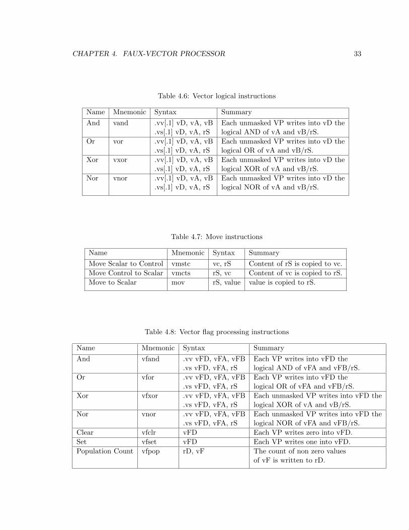
Table 4.6: Vector logical instructions
Name Mnemonic Syntax Summary
And vand .vv[.1] vD, vA, vB Each unmasked VP writes into vD the
.vs[.1] vD, vA, rS logical AND of vA and vB/rS.
Or vor .vv[.1] vD, vA, vB Each unmasked VP writes into vD the
.vs[.1] vD, vA, rS logical OR of vA and vB/rS.
Xor vxor .vv[.1] vD, vA, vB Each unmasked VP writes into vD the
.vs[.1] vD, vA, rS logical XOR of vA and vB/rS.
Nor vnor .vv[.1] vD, vA, vB Each unmasked VP writes into vD the
.vs[.1] vD, vA, rS logical NOR of vA and vB/rS.
Table 4.7: Move instructions
Name Mnemonic Syntax Summary
Move Scalar to Control vmstc vc, rS Content of rS is copied to vc.
Move Control to Scalar vmcts rS, vc Content of vc is copied to rS.
Move to Scalar mov rS, value value is copied to rS.
Table 4.8: Vector flag processing instructions
Name Mnemonic Syntax Summary
And vfand .vv vFD, vFA, vFB Each VP writes into vFD the
.vs vFD, vFA, rS logical AND of vFA and vFB/rS.
Or vfor .vv vFD, vFA, vFB Each VP writes into vFD the
.vs vFD, vFA, rS logical OR of vFA and vFB/rS.
Xor vfxor .vv vFD, vFA, vFB Each unmasked VP writes into vFD the
.vs vFD, vFA, rS logical XOR of vA and vB/rS.
Nor vnor .vv vFD, vFA, vFB Each unmasked VP writes into vFD the
.vs vFD, vFA, rS logical NOR of vFA and vFB/rS.
Clear vfclr vFD Each VP writes zero into vFD.
Set vfset vFD Each VP writes one into vFD.
Population Count vfpop rD, vF The count of non zero values
of vF is written to rD.
CHAPTER 4. FAUX-VECTOR PROCESSOR 34
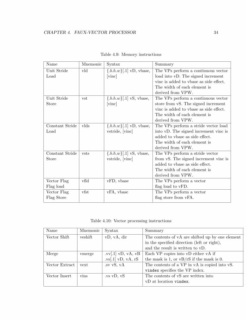
Table 4.9: Memory instructions
Name Mnemonic Syntax Summary
Unit Stride vld {.b.h.w}[.1] vD, vbase, The VPs perform a continuous vector
Load [vinc] load into vD. The signed increment
vinc is added to vbase as side e↵ect.
The width of each element is
derived from VPW.
Unit Stride vst {.b.h.w}[.1] vS, vbase, The VPs perform a continuous vector
Store [vinc] store from vS. The signed increment
vinc is added to vbase as side e↵ect.
The width of each element is
derived from VPW.
Constant Stride vlds {.b.h.w}[.1] vD, vbase, The VPs perform a stride vector load
Load vstride, [vinc] into vD. The signed increment vinc is
added to vbase as side e↵ect.
The width of each element is
derived from VPW.
Constant Stride vsts {.b.h.w}[.1] vS, vbase, The VPs perform a stride vector
Store vstride, [vinc] from vS. The signed increment vinc is
added to vbase as side e↵ect.
The width of each element is
derived from VPW.
Vector Flag vfld vFD, vbase The VPs perform a vector
Flag load flag load to vFD.
Vector Flag vfst vFA, vbase The VPs perform a vector
Flag Store flag store from vFA.
Table 4.10: Vector processing instructions
Name Mnemonic Syntax Summary
Vector Shift veshift vD, vA, dir The contents of vA are shifted up by one element
in the specified direction (left or right),
and the result is written to vD.
Merge vmerge .vv[.1] vD, vA, vB Each VP copies into vD either vA if
.vs[.1] vD, vA, rS the mask is 1, or vB/rS if the mask is 0.
Vector Extract vext .sv vS, vA The contents of a VP in vA is copied into vS.
vindex specifies the VP index.
Vector Insert vins .vs vD, vS The contents of vS are written into
vD at location vindex.
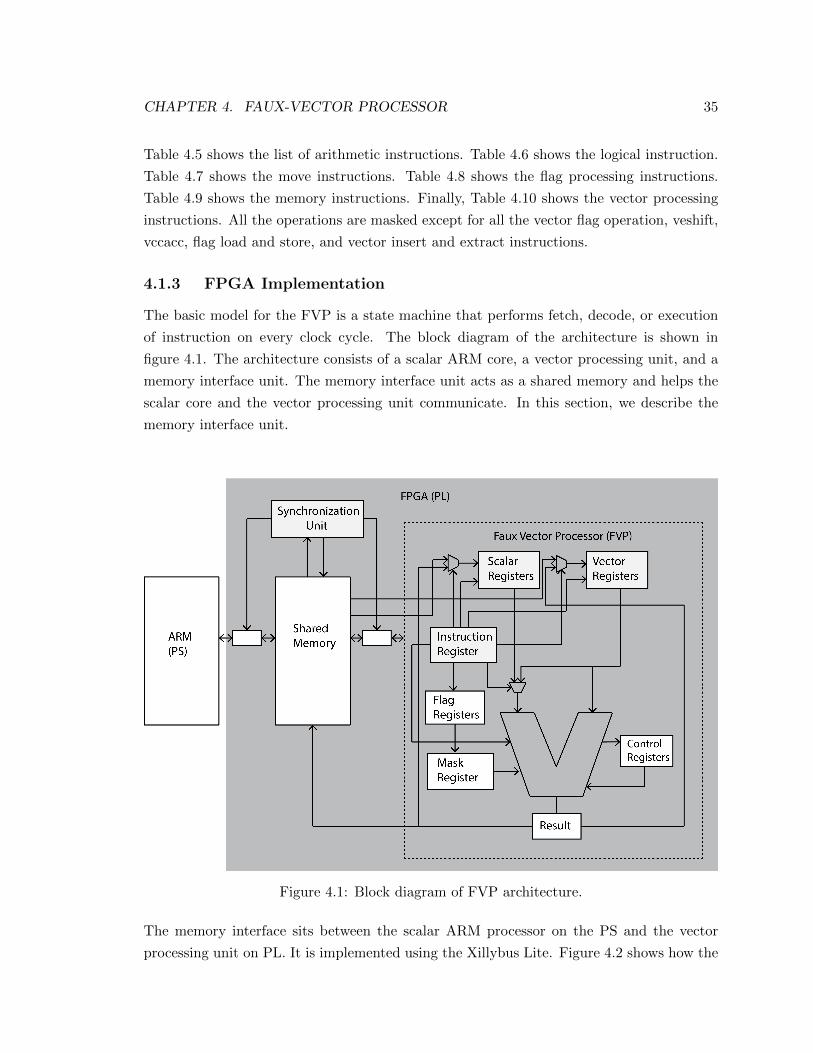
CHAPTER 4. FAUX-VECTOR PROCESSOR 35
Table 4.5 shows the list of arithmetic instructions. Table 4.6 shows the logical instruction.
Table 4.7 shows the move instructions. Table 4.8 shows the flag processing instructions.
Table 4.9 shows the memory instructions. Finally, Table 4.10 shows the vector processing
instructions. All the operations are masked except for all the vector flag operation, veshift,
vccacc, flag load and store, and vector insert and extract instructions.
4.1.3 FPGA Implementation
The basic model for the FVP is a state machine that performs fetch, decode, or execution
of instruction on every clock cycle. The block diagram of the architecture is shown in
figure 4.1. The architecture consists of a scalar ARM core, a vector processing unit, and a
memory interface unit. The memory interface unit acts as a shared memory and helps the
scalar core and the vector processing unit communicate. In this section, we describe the
memory interface unit.
Figure 4.1: Block diagram of FVP architecture.
The memory interface sits between the scalar ARM processor on the PS and the vector
processing unit on PL. It is implemented using the Xillybus Lite. Figure 4.2 shows how the
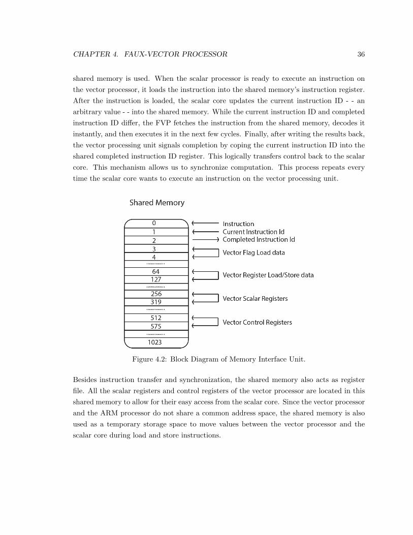
CHAPTER 4. FAUX-VECTOR PROCESSOR 36
shared memory is used. When the scalar processor is ready to execute an instruction on
the vector processor, it loads the instruction into the shared memory’s instruction register.
After the instruction is loaded, the scalar core updates the current instruction ID - - an
arbitrary value - - into the shared memory. While the current instruction ID and completed
instruction ID di↵er, the FVP fetches the instruction from the shared memory, decodes it
instantly, and then executes it in the next few cycles. Finally, after writing the results back,
the vector processing unit signals completion by coping the current instruction ID into the
shared completed instruction ID register. This logically transfers control back to the scalar
core. This mechanism allows us to synchronize computation. This process repeats every
time the scalar core wants to execute an instruction on the vector processing unit.
Figure 4.2: Block Diagram of Memory Interface Unit.
Besides instruction transfer and synchronization, the shared memory also acts as register
file. All the scalar registers and control registers of the vector processor are located in this
shared memory to allow for their easy access from the scalar core. Since the vector processor
and the ARM processor do not share a common address space, the shared memory is also
used as a temporary storage space to move values between the vector processor and the
scalar core during load and store instructions.
CHAPTER 4. FAUX-VECTOR PROCESSOR 37
4.2 Programming the FVP from Processing System
In this section, we will give a basic outline of the interface to interact with the FVP. When
a programmer wants to execute some operation, there are two possible paths: to execute
the operation on the ARM processor, running the Linux operation system, or to make use
of the vector processing unit. To execute an instruction on the vector processing unit, the
user uses library calls written in C. These library calls are like any ordinary procedure calls
and they hide details regarding instruction execution and synchronization. Typical library
calls are shown in listing 4.1. Therefore, to perform any computation, the user simply can
make these library calls in the middle of their program after setting parameters like VL and
VPW.
void vld(int dest , int src1 , int inc , int mask);void vlds(int dest , int src1 , int stride , int inc , int mask);void vst(int src , int base , int inc , int mask);void vsts(int src , int base , int stride ,int inc , int mask);void vadd(int dest , int src1 , int src2 ,int mask);void vabs(int dest , int src1 , int mask);void vmul(int dest , int src1 , int src2 , int mask);void vand(int dest , int src1 , int src2 , int mask);void vor(int dest , int src1 , int src2 , int mask);void vnor(int dest , int src1 , int src2 , int mask);void vmac(int src1 , int src2 , int mask);void vccacc(int dest);void veshift(int dest , int dir);void vfld(int dest ,int64_t value);void vfand(int dest , int src1 , int src2);void vfor(int dest , int src1 , int src2);void vfxor(int dest , int src1 , int src2);void vfnor(int dest , int src1 , int src2);void vfclr(int dest);void vfset(int dest);void vmin(int dest ,int src1 , int src2 , int mask);void vmax(int dest ,int src1 , int src2 , int mask);
Listing 4.1: Few example library calls for FVP
Rather than using the library calls, a vectorizing compiler could be used to target our FVP.
Even though our tools currently do not include a vectorizing compiler, we are confident
that this support could be added later. We discuss this possibility in Chapter 6.
4.2.1 Design Examples
In this section, five benchmarks, representative of common applications are chosen to
demonstrate the ease of use and advantages of the FVP. For each of the examples below,
we present the representation in C, and equivalent code using our library calls.

CHAPTER 4. FAUX-VECTOR PROCESSOR 38
Matrix Multiplication
Matrix Multiplication is a very popular operation in mathematics with wide range of ap-
plications. The code in Listing 4.2 shows matrix multiplication code in C, and the code in
Listing 4.3 shows the library call equivalent of the same C code. In the library call version,
one of the dimensions is handled by vectoring (removing) the inner loop.
1 void matrix_mul_c(int ib[n][n], int ic[n][n], int result[n][n], intn){
2 int i,j,k,sum;3 for(i = 0; i < n; i++){4 for (j = 0; j < n; j++){5 sum = 0;6 for (k = 0; k < n; k++) {7 sum += ib[i][k]*ic[k][j];8 }9 result[i][j] = sum;10 }11 }12 }
Listing 4.2: Matrix multiplication in C
1 void matrix_mul_lib(int ib[n][n], int ic[n][n], int result[n][n],int n){
2
3 vmstc(VL ,n);4 vmstc(VPW ,4); // width of the data in bytes
5
6 vmstc(STRIDE1 ,n); // row width
7 vmstc(STRIDE2 ,1);8 vmstc(INC1 ,1);9 vmstc(INC2 ,n);10
11 vmstc(BASE0 ,result);12 vmstc(BASE1 ,ib);13 vmstc(BASE2 ,ic);14
15 int i,j;16 for(i=0;i<n;i++){17 vld(VR2 ,BASE1 ,INC2 ,vfmask0);18 vmstc(BASE2 , &ic);19 for(j=0; j<n;j++){20 vlds(VR1 ,BASE2 ,STRIDE1 ,INC1 ,vfmask0);21 vmac(VR2 ,VR1 ,vfmask0);22 vccacc(VR3);23 veshift(VR3 ,LEFT);24 }25 vsts(VR3 ,BASE0 ,STRIDE2 ,INC2 ,vfmask0);26 }27 }
Listing 4.3: Matrix multiplication in Library Calls
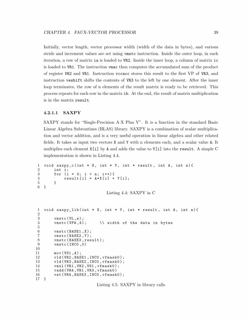
CHAPTER 4. FAUX-VECTOR PROCESSOR 39
Initially, vector length, vector processor width (width of the data in bytes), and various
stride and increment values are set using vmstc instruction. Inside the outer loop, in each
iteration, a row of matrix ia is loaded to VR2. Inside the inner loop, a column of matrix ic
is loaded to VR1. The instruction vmac then computes the accumulated sum of the product
of register VR2 and VR1. Instruction vccacc stores this result to the first VP of VR3, and
instruction veshift shifts the contents of VR3 to the left by one element. After the inner
loop terminates, the row of n elements of the result matrix is ready to be retrieved. This
process repeats for each row in the matrix ib. At the end, the result of matrix multiplication
is in the matrix result.
4.2.1.1 SAXPY
SAXPY stands for “Single-Precision A·X Plus Y”. It is a function in the standard Basic
Linear Algebra Subroutines (BLAS) library. SAXPY is a combination of scalar multiplica-
tion and vector addition, and is a very useful operation in linear algebra and other related
fields. It takes as input two vectors X and Y with n elements each, and a scalar value A. It
multiplies each element X[i] by A and adds the value to Y[i] into the result. A simple C
implementation is shown in Listing 4.4.
1 void saxpy_c(int * X, int * Y, int * result , int A, int n){2 int i;3 for (i = 0; i < n; i++){4 result[i] = A*X[i] + Y[i];5 }6 }
Listing 4.4: SAXPY in C
1 void saxpy_lib(int * X, int * Y, int * result , int A, int n){2
3 vmstc(VL ,n);4 vmstc(VPW ,4); \\ width of the data in bytes5
6 vmstc(BASE1 ,X);7 vmstc(BASE2 ,Y);8 vmstc(BASE3 ,result);9 vmstc(INC0 ,0)10
11 mov(VS1 ,A);12 vld(VR2 ,BASE1 ,INC0 ,vfmask0);13 vld(VR3 ,BASE2 ,INC0 ,vfmask0);14 vmul(VR1 ,VR2 ,VS1 ,vfmask0);15 vadd(VR4 ,VR1 ,VR3 ,vfmask0)16 vst(VR4 ,BASE3 ,INC0 ,vfmask0);17 }
Listing 4.5: SAXPY in library calls
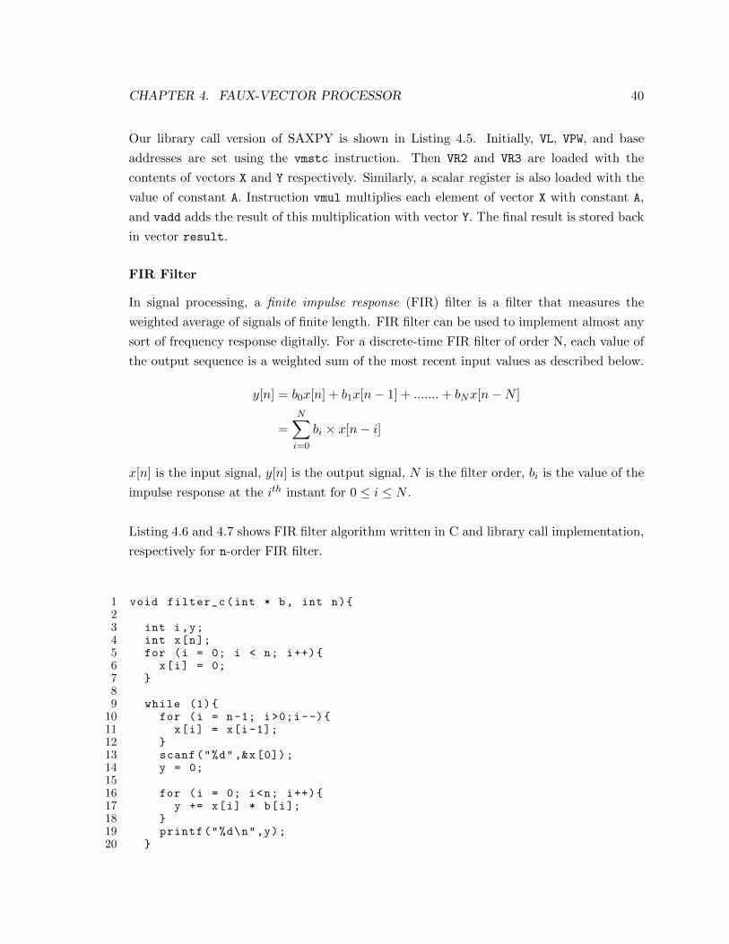
CHAPTER 4. FAUX-VECTOR PROCESSOR 40
Our library call version of SAXPY is shown in Listing 4.5. Initially, VL, VPW, and base
addresses are set using the vmstc instruction. Then VR2 and VR3 are loaded with the
contents of vectors X and Y respectively. Similarly, a scalar register is also loaded with the
value of constant A. Instruction vmul multiplies each element of vector X with constant A,
and vadd adds the result of this multiplication with vector Y. The final result is stored back
in vector result.
FIR Filter
In signal processing, a finite impulse response (FIR) filter is a filter that measures the
weighted average of signals of finite length. FIR filter can be used to implement almost any
sort of frequency response digitally. For a discrete-time FIR filter of order N, each value of
the output sequence is a weighted sum of the most recent input values as described below.
y[n] = b0x[n] + b1x[n� 1] + .......+ bNx[n�N ]
=
NX
i=0
bi ⇥ x[n� i]
x[n] is the input signal, y[n] is the output signal, N is the filter order, bi is the value of the
impulse response at the i
thinstant for 0 i N .
Listing 4.6 and 4.7 shows FIR filter algorithm written in C and library call implementation,
respectively for n-order FIR filter.
1 void filter_c(int * b, int n){2
3 int i,y;4 int x[n];5 for (i = 0; i < n; i++){6 x[i] = 0;7 }8
9 while (1){10 for (i = n-1; i>0;i--){11 x[i] = x[i-1];12 }13 scanf("%d",&x[0]);14 y = 0;15
16 for (i = 0; i<n; i++){17 y += x[i] * b[i];18 }19 printf("%d\n",y);20 }
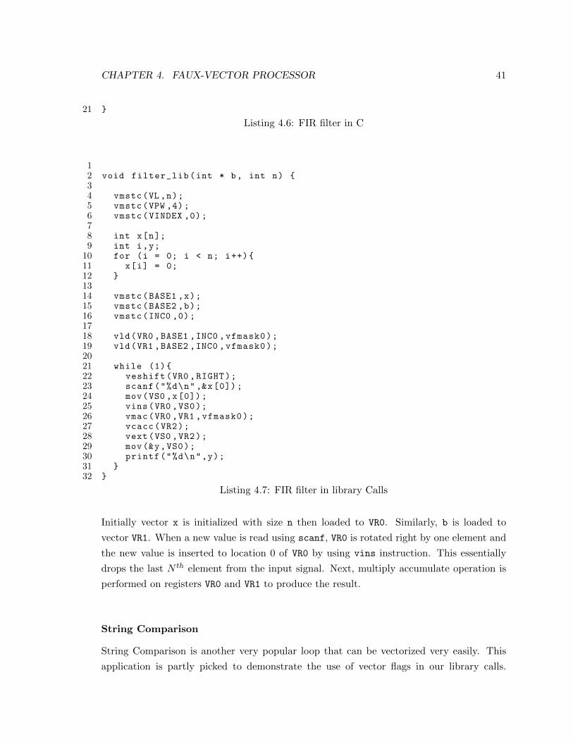
CHAPTER 4. FAUX-VECTOR PROCESSOR 41
21 }
Listing 4.6: FIR filter in C
1
2 void filter_lib(int * b, int n) {3
4 vmstc(VL ,n);5 vmstc(VPW ,4);6 vmstc(VINDEX ,0);7
8 int x[n];9 int i,y;10 for (i = 0; i < n; i++){11 x[i] = 0;12 }13
14 vmstc(BASE1 ,x);15 vmstc(BASE2 ,b);16 vmstc(INC0 ,0);17
18 vld(VR0 ,BASE1 ,INC0 ,vfmask0);19 vld(VR1 ,BASE2 ,INC0 ,vfmask0);20
21 while (1){22 veshift(VR0 ,RIGHT);23 scanf("%d\n",&x[0]);24 mov(VS0 ,x[0]);25 vins(VR0 ,VS0);26 vmac(VR0 ,VR1 ,vfmask0);27 vcacc(VR2);28 vext(VS0 ,VR2);29 mov(&y,VS0);30 printf("%d\n",y);31 }32 }
Listing 4.7: FIR filter in library Calls
Initially vector x is initialized with size n then loaded to VR0. Similarly, b is loaded to
vector VR1. When a new value is read using scanf, VR0 is rotated right by one element and
the new value is inserted to location 0 of VR0 by using vins instruction. This essentially
drops the last N
thelement from the input signal. Next, multiply accumulate operation is
performed on registers VR0 and VR1 to produce the result.
String Comparison
String Comparison is another very popular loop that can be vectorized very easily. This
application is partly picked to demonstrate the use of vector flags in our library calls.
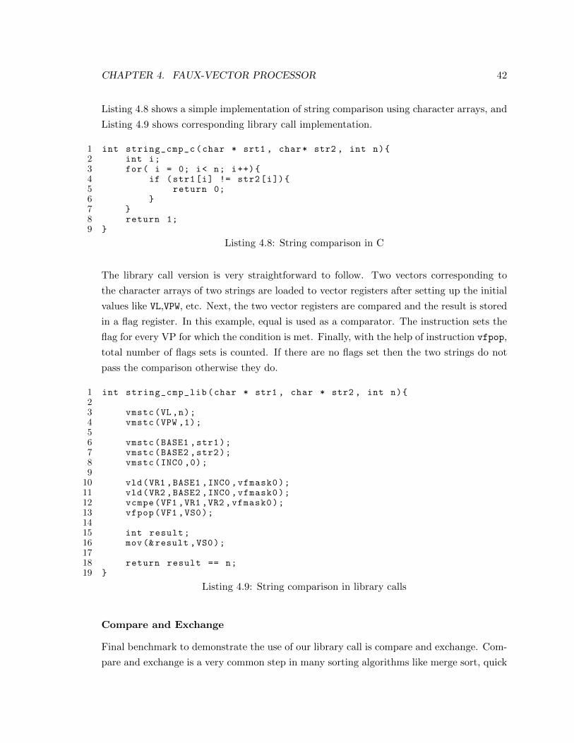
CHAPTER 4. FAUX-VECTOR PROCESSOR 42
Listing 4.8 shows a simple implementation of string comparison using character arrays, and
Listing 4.9 shows corresponding library call implementation.
1 int string_cmp_c(char * srt1 , char* str2 , int n){2 int i;3 for( i = 0; i< n; i++){4 if (str1[i] != str2[i]){5 return 0;6 }7 }8 return 1;9 }
Listing 4.8: String comparison in C
The library call version is very straightforward to follow. Two vectors corresponding to
the character arrays of two strings are loaded to vector registers after setting up the initial
values like VL,VPW, etc. Next, the two vector registers are compared and the result is stored
in a flag register. In this example, equal is used as a comparator. The instruction sets the
flag for every VP for which the condition is met. Finally, with the help of instruction vfpop,
total number of flags sets is counted. If there are no flags set then the two strings do not
pass the comparison otherwise they do.
1 int string_cmp_lib(char * str1 , char * str2 , int n){2
3 vmstc(VL ,n);4 vmstc(VPW ,1);5
6 vmstc(BASE1 ,str1);7 vmstc(BASE2 ,str2);8 vmstc(INC0 ,0);9
10 vld(VR1 ,BASE1 ,INC0 ,vfmask0);11 vld(VR2 ,BASE2 ,INC0 ,vfmask0);12 vcmpe(VF1 ,VR1 ,VR2 ,vfmask0);13 vfpop(VF1 ,VS0);14
15 int result;16 mov(&result ,VS0);17
18 return result == n;19 }
Listing 4.9: String comparison in library calls
Compare and Exchange
Final benchmark to demonstrate the use of our library call is compare and exchange. Com-
pare and exchange is a very common step in many sorting algorithms like merge sort, quick

CHAPTER 4. FAUX-VECTOR PROCESSOR 43
sort, etc. The application also demostrates the use of flag registers. Listing 4.10 shows a
simple compare and exchange algorithm written in C.
1 void cmp_exc_c(int * a, int * b, int n){2 int i;3 for(i = 0;i< n; i++){4 if (compare(a[i],b[i]) >0){5 swap(&a[i],&b[i]);6 }7 }8 }
Listing 4.10: Compare and exchange in C
1 void cmp_exc_lib(int * a, int * b, int n){2
3 vmstc(VL ,n);4 vmstc(VPW ,4); // size of the data in bytes
5
6 vmstc(BASE1 ,a);7 vmstc(BASE2 ,b);8 vmstc(INC0 ,0);9
10 vld(VR2 ,BASE1 ,INC0 ,vfmask0);11 vld(VR3 ,BASE2 ,INC0 ,vfmask0);12 cmplt(vfmask1 ,VR2 ,VR3 ,vfmask0);13
14 //swap based on flag
15 vadd(VR2 ,VR2 ,VR3 ,vfmask1);16 vsub(VR3 ,VR2 ,VR3 ,vfmask1);17 vsub(VR2 ,VR2 ,VR3 ,vfmask1);18
19 vst(VR2 ,BASE1 ,INC0 ,vfmask0);20 vst(VR3 ,BASE2 ,INC0 ,vfmask0);21 }
Listing 4.11: Compare and exchange in library calls
Listing 4.11 shows the same algorithm written in terms of our library calls. After setting
up necessary control registers, the data is loaded to vector registers. Next, a comparison
operation is performed, less than in our example. Like in string comparison, a vector flag
is not set for every comparison that passes. Based on this vector flag, a simple swap is
performed using masked vadd and vsub as described in Algorithm 2. Finally, the results
are stored back after the swap.
4.3 Summary
The FVP and its support library as described in this section represents a first successful step
towards large scale FPGA-based reconfigurable co-processor. With the help of library calls,

CHAPTER 4. FAUX-VECTOR PROCESSOR 44
Algorithm 2 Swap using add and subtract
Require: Input a and b
1: a a+ b
2: b a� b
3: a a� b
the architecture provides a level of abstraction which makes it possible for software engineers
to make use of custom co-processors without having to deal with hardware directly. In the
near future, system like ours will reduce the complexity of using hardware for software
development so that it can reach the degree of convenience that software developers have
long become used to. More importantly, the FPGA’s reconfigurability gives this architecture
the flexibility to modify and improve the design without any significant financial or technical
ramifications. FPGA-based co-processor avoids the need to decide on a set of specialized
units at chip design time. Rather, new or improved specialized units could be added to the
chip at any time. At the same time, no chip resources are wasted for specialized functionality
that a particular system installation may never actually need.

5. Faux-Vector Processor
Performance Estimation
The current implementation of the FVP described in Chapter 4 is a first step towards
creating a configurable co-processor tightly couple with a GPP. In this Chapter, we describe
the e�ciency, both in terms of performance and energy, of the design described in Chapter 4.
Specifically, we describe the components of our infrastructure necessary to execute, verify,
and evaluate instructions for the FVP.
5.1 Methodology
Along with our hardware implementation of FVP, we also implemented a software simula-
tion of the the co-processor written in the C programming language. The reason behind the
software simulation is to accurately compare the performance between implementing the
same exact logic on hardware and software. All of the instructions for the vector processor
were tested and verified both on hardware and software implementations of the FVP. Fur-
thermore, we also compare the performance of implementing all of our benchmark programs
described in Section 4.2.1 purely on the ARM processor and on the ARM processor with
FVP as a tightly coupled co-processor. Finally, we begin analysis of the power consumed
by the hardware implementation of the FVP.
5.2 Hardware Utilization
Figure 5.1 shows the estimated hardware resource utilization with and without the current
implementation of the FVP on the Zynq device. A functional Zynq system without FVP
core includes a VGA core to support VGA interface, two AXI buses, and Xillybus-lite core
to help aid the communication between ARM (PS) and FVP (PL). We can see from the
resource utilization table that the vector processor mainly consumes logic slices. As a result,
45

CHAPTER 5. FAUX-VECTOR PROCESSOR PERFORMANCE ESTIMATION 46
0 10 20 30 40 50 60 70 80 90 100
FF
LUT
Memory LUT
I/O
BRAM
BUFG
PLL
4
14
17
34
1
1
25
3
5
1
34
1
1
25
Utilization
Without Faux Vector Processor
With Faux Vector Processor
Figure 5.1: Resource utilization of hardware implementation with and without FVP.
the logic overhead is about 4% of FF, 14% of LUT, and 17% of Memory LUT. FF are flip-
flops, registers that store machine state. LUT are lookup tables, hardware that supports
implementation of custom logic. The co-processor design also utilizes a small percent of
digital signal processing unit called DSP48 slice to support e�cient multiplication.
As we can see from the graph, FVP is only responsible for a small fraction of the Zynq’s
resources. Hardware resources like PLL, BUFG, BRAM and IO are not utilized by the FVP
and are mainly consumed by Xillybus architecture. We believe that the overall resource
utilization can be further reduced if we replace Xillybus with our synchronization core.
5.3 Vector Performance
In this section, we measure the performance of executing instructions on the software versus
the hardware implementation of the FVP. We wanted to measure the performance of imple-
menting the same circuit on software and hardware as this would allow us to measure the
relative e�ciency of running the same program on hardware and software. To measure the
execution time, each of the instruction is performed 10000 times and the best average time
of these runs over 100 repetitions is recorded. The process is repeated for varying vector
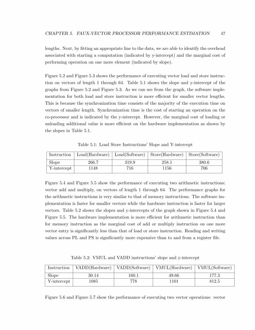
CHAPTER 5. FAUX-VECTOR PROCESSOR PERFORMANCE ESTIMATION 47
lengths. Next, by fitting an appropriate line to the data, we are able to identify the overhead
associated with starting a computation (indicated by y-intercept) and the marginal cost of
performing operation on one more element (indicated by slope).
Figure 5.2 and Figure 5.3 shows the performance of executing vector load and store instruc-
tion on vectors of length 1 through 64. Table 5.1 shows the slope and y-intercept of the
graphs from Figure 5.2 and Figure 5.3. As we can see from the graph, the software imple-
mentation for both load and store instruction is more e�cient for smaller vector lengths.
This is because the synchronization time consists of the majority of the execution time on
vectors of smaller length. Synchronization time is the cost of starting an operation on the
co-processor and is indicated by the y-intercept. However, the marginal cost of loading or
unloading additional value is more e�cient on the hardware implementation as shown by
the slopes in Table 5.1.
Table 5.1: Load Store Instructions’ Slope and Y-intercept
Instruction Load(Hardware) Load(Software) Store(Hardware) Store(Software)
Slope 266.7 319.9 258.1 380.6
Y-intercept 1148 716 1156 706
Figure 5.4 and Figure 5.5 show the performance of executing two arithmetic instructions:
vector add and multiply, on vectors of length 1 through 64. The performance graphs for
the arithmetic instructions is very similar to that of memory instructions. The software im-
plementation is faster for smaller vectors while the hardware instruction is faster for larger
vectors. Table 5.2 shows the slopes and y-intercepts of the graph shown in Figure 5.4 and
Figure 5.5. The hardware implementation is more e�cient for arithmetic instruction than
for memory instruction as the marginal cost of add or multiply instruction on one more
vector entry is significantly less than that of load or store instruction. Reading and writing
values across PL and PS is significantly more expensive than to and from a register file.
Table 5.2: VMUL and VADD instructions’ slope and y-intercept
Instruction VADD(Hardware) VADD(Software) VMUL(Hardware) VMUL(Software)
Slope 30.14 160.1 49.66 177.3
Y-intercept 1085 778 1101 812.5
Figure 5.6 and Figure 5.7 show the performance of executing two vector operations: vector
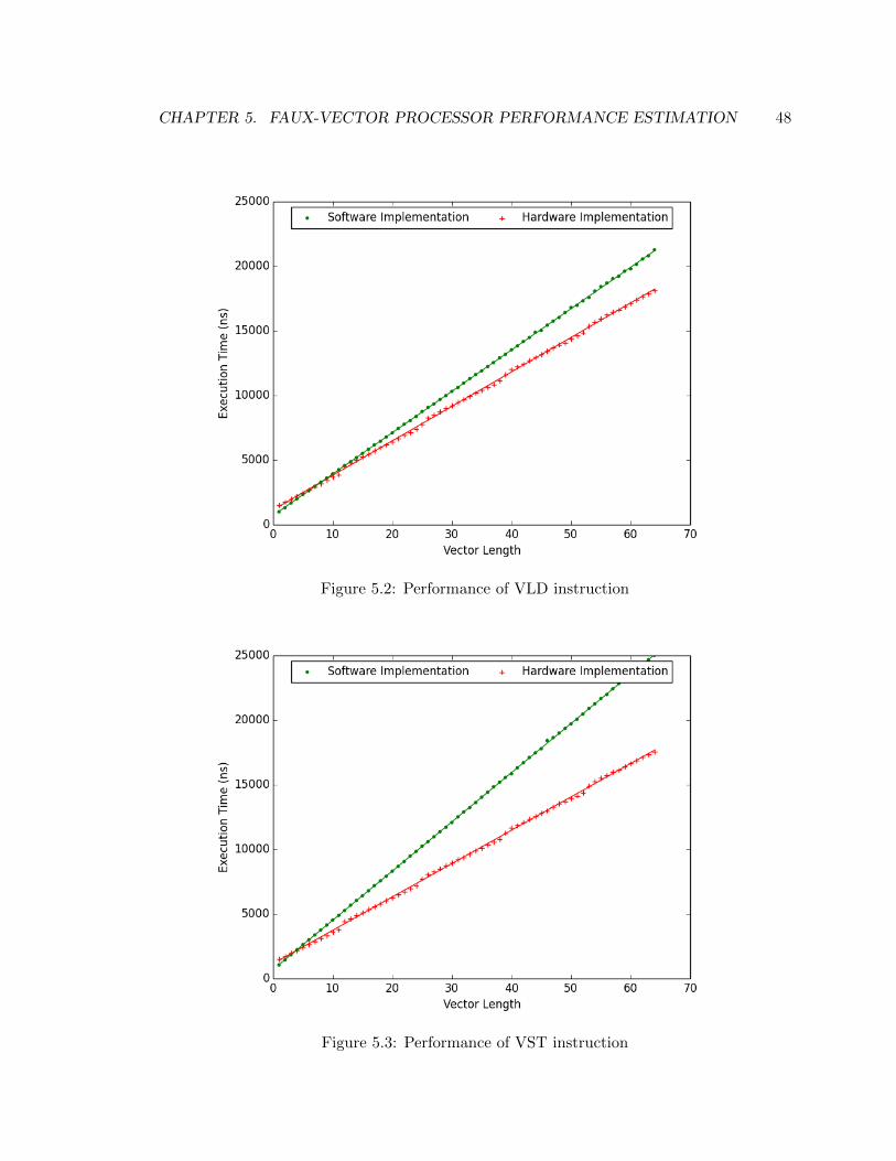
CHAPTER 5. FAUX-VECTOR PROCESSOR PERFORMANCE ESTIMATION 48
Figure 5.2: Performance of VLD instruction
Figure 5.3: Performance of VST instruction
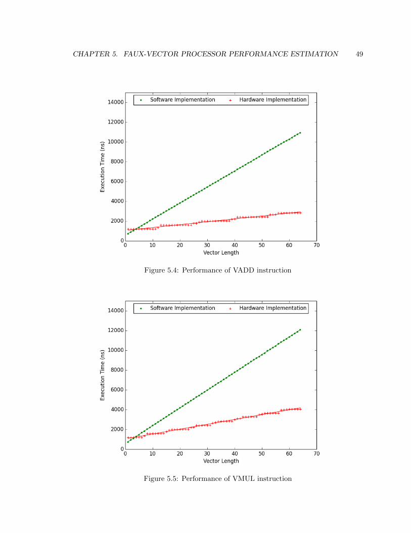
CHAPTER 5. FAUX-VECTOR PROCESSOR PERFORMANCE ESTIMATION 49
Figure 5.4: Performance of VADD instruction
Figure 5.5: Performance of VMUL instruction
CHAPTER 5. FAUX-VECTOR PROCESSOR PERFORMANCE ESTIMATION 50
shift and multiply accumulate on vectors of length 1 through 64. The execution of the
vector instructions is also faster on the hardware compared to the software version of the
FVP. Like memory and arithmetic instructions, the performance gain of hardware imple-
mentation is only realized when the vectors become large as for smaller vectors the overhead
of instruction synchronization is high. Table 5.3 shows the slopes and y-intercepts for the
graphs in Figure 5.6 and Figure 5.7.
Table 5.3: VESHIFT and VMAC instructions’ slope and y-intercept
Instruction VESHIFT(Hardware) VESHIFT(Software) VMAC(Hardware) VMAC(Software)
Slope 19.24 127.5 48.86 152.8
Y-intercept 1066 580.3 1055 568.3
Figure 5.6: Performance of VESHIFT instruction
Figure 5.8 shows the performance of executing a vector flag operation on hardware vs soft-
ware implementation of the FVP. Unlike other operations, the software implementation is
significantly faster than the hardware implementation of the FVP. Flag operations are ba-
sically constant time operations and they do not depend on the vector length. As a result,
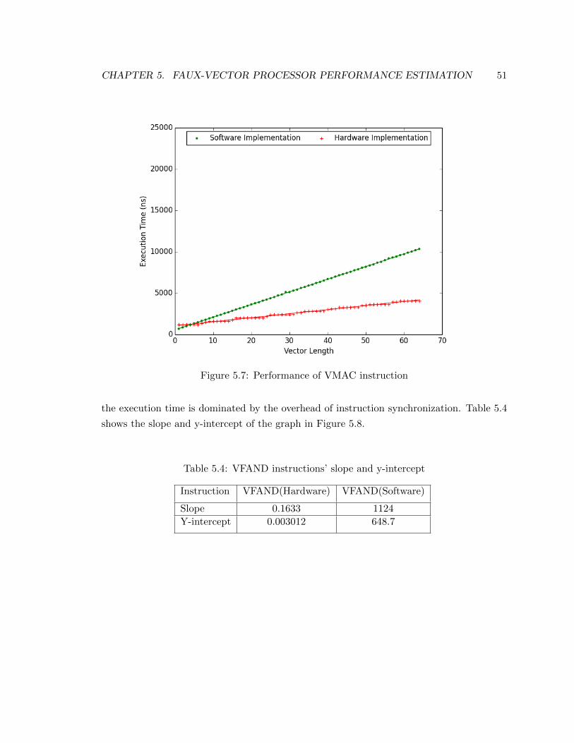
CHAPTER 5. FAUX-VECTOR PROCESSOR PERFORMANCE ESTIMATION 51
Figure 5.7: Performance of VMAC instruction
the execution time is dominated by the overhead of instruction synchronization. Table 5.4
shows the slope and y-intercept of the graph in Figure 5.8.
Table 5.4: VFAND instructions’ slope and y-intercept
Instruction VFAND(Hardware) VFAND(Software)
Slope 0.1633 1124
Y-intercept 0.003012 648.7

CHAPTER 5. FAUX-VECTOR PROCESSOR PERFORMANCE ESTIMATION 52
Figure 5.8: Performance of VFAND operation
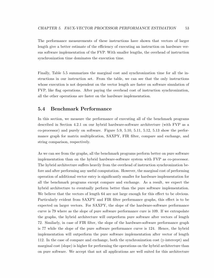
CHAPTER 5. FAUX-VECTOR PROCESSOR PERFORMANCE ESTIMATION 53
The performance measurements of these instructions have shown that vectors of larger
length give a better estimate of the e�ciency of executing an instruction on hardware ver-
sus software implementation of the FVP. With smaller lengths, the overhead of instruction
synchronization time dominates the execution time.
Finally, Table 5.5 summarizes the marginal cost and synchronization time for all the in-
structions in our instruction set. From the table, we can see that the only instructions
whose execution is not dependent on the vector length are faster on software simulation of
FVP, like flag operations. After paying the overhead cost of instruction synchronization,
all the other operations are faster on the hardware implementation.
5.4 Benchmark Performance
In this section, we measure the performance of executing all of the benchmark programs
described in Section 4.2.1 on our hybrid hardware-software architecture (with FVP as a
co-processor) and purely on software. Figure 5.9, 5.10, 5.11, 5.12, 5.13 show the perfor-
mance graph for matrix multiplication, SAXPY, FIR filter, compare and exchange, and
string comparison, respectively.
As we can see from the graphs, all the benchmark programs perform better on pure software
implementation than on the hybrid hardware-software system with FVP as co-processor.
The hybrid architecture su↵ers heavily from the overhead of instruction synchronization be-
fore and after performing any useful computation. However, the marginal cost of performing
operation of additional vector entry is significantly smaller for hardware implementation for
all the benchmark programs except compare and exchange. As a result, we expect the
hybrid architecture to eventually perform better than the pure software implementation.
We believe that the vectors of length 64 are not large enough for this e↵ect to be obvious.
Particularly evident from SAXPY and FIR filter performance graphs, this e↵ect is to be
expected on larger vectors. For SAXPY, the slope of the hardware-software performance
curve is 79 where as the slope of pure software performance cure is 109. If we extrapolate
the graphs, the hybrid architecture will outperform pure software after vectors of length
72. Similarly, in case of FIR filter, the slope of the hardware-software performance graph
is 77 while the slope of the pure software performance curve is 124. Hence, the hybrid
implementation will outperform the pure software implementation after vector of length
112. In the case of compare and exchange, both the synchronization cost (y-intercept) and
marginal cost (slope) is higher for performing the operations on the hybrid architecture than
on pure software. We accept that not all applications are well suited for this architecture
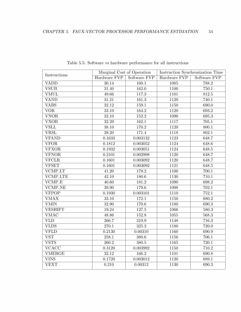
CHAPTER 5. FAUX-VECTOR PROCESSOR PERFORMANCE ESTIMATION 54
Table 5.5: Software vs hardware performance for all instructions
Instructions
Marginal Cost of Operation Instruction Synchronization Time
Hardware FVP Software FVP Hardware FVP Software FVP
VADD 30.14 160.1 1085 788.2
VSUB 31.40 162.0 1100 750.1
VMUL 49.66 117.3 1101 812.5
VAND 31.21 161.3 1120 740.1
VABS 32.12 159.1 1150 690.0
VOR 33.10 164.2 1120 693.2
VNOR 32.10 152.2 1090 695.3
VXOR 32.29 162.1 1117 705.1
VSLL 38.10 170.2 1120 800.1
VRSL 39.20 171.4 1118 802.1
VFAND 0.1633 0.003132 1123 648.7
VFOR 0.1812 0.003052 1124 648.6
VFXOR 0.1932 0.003051 1124 648.5
VFNOR 0.2101 0.002998 1120 648.7
VFCLR 0.1601 0.003092 1120 648.7
VFSET 0.1601 0.003092 1121 648.5
VCMP LT 41.20 178.2 1100 700.1
VCMP LTE 42.10 180.6 1130 710.1
VCMP E 40.60 181.2 1090 698.2
VCMP NE 39.90 179.6 1098 702.1
VFPOP 0.1930 0.003101 1110 752.1
VMAX 33.10 172.1 1150 680.2
VMIN 32.90 170.6 1180 690.3
VESHIFT 19.24 127.5 1066 580.3
VMAC 48.86 152.8 1055 568.3
VLD 266.7 319.9 1148 716.3
VLDS 270.1 325.2 1180 720.0
VFLD 0.2130 0.00310 1160 690.9
VST 258.1 380.6 1156 706.1
VSTS 260.2 380.5 1165 720.1
VCACC 0.3120 0.003992 1150 710.2
VMERGE 32.12 166.2 1101 690.8
VINS 0.1720 0.003012 1120 689.1
VEXT 0.210 0.00312 1130 690.3
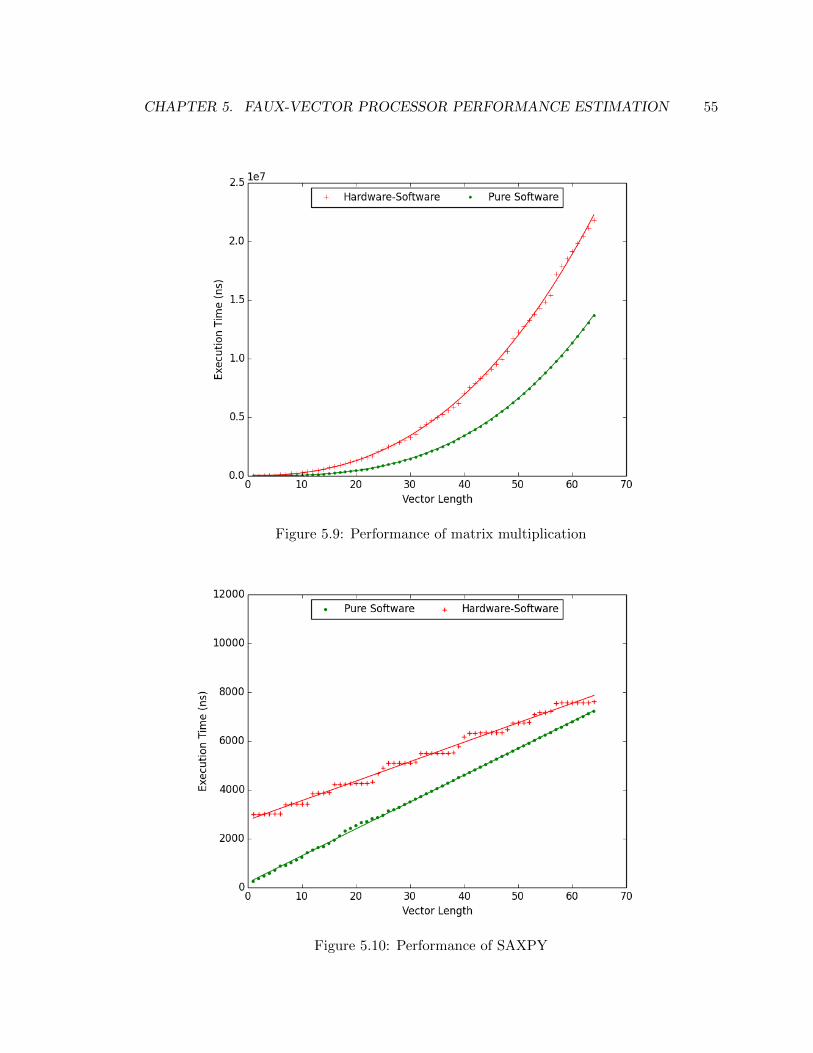
CHAPTER 5. FAUX-VECTOR PROCESSOR PERFORMANCE ESTIMATION 55
Figure 5.9: Performance of matrix multiplication
Figure 5.10: Performance of SAXPY

CHAPTER 5. FAUX-VECTOR PROCESSOR PERFORMANCE ESTIMATION 56
Figure 5.11: Performance of FIR filter
Figure 5.12: Performance of compare and exchange
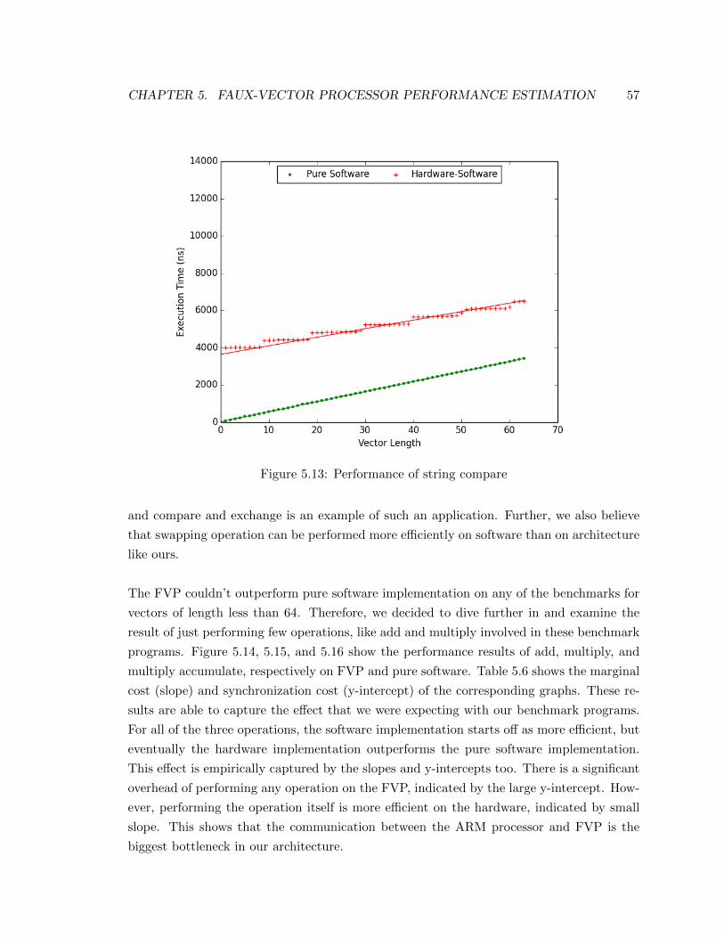
CHAPTER 5. FAUX-VECTOR PROCESSOR PERFORMANCE ESTIMATION 57
Figure 5.13: Performance of string compare
and compare and exchange is an example of such an application. Further, we also believe
that swapping operation can be performed more e�ciently on software than on architecture
like ours.
The FVP couldn’t outperform pure software implementation on any of the benchmarks for
vectors of length less than 64. Therefore, we decided to dive further in and examine the
result of just performing few operations, like add and multiply involved in these benchmark
programs. Figure 5.14, 5.15, and 5.16 show the performance results of add, multiply, and
multiply accumulate, respectively on FVP and pure software. Table 5.6 shows the marginal
cost (slope) and synchronization cost (y-intercept) of the corresponding graphs. These re-
sults are able to capture the e↵ect that we were expecting with our benchmark programs.
For all of the three operations, the software implementation starts o↵ as more e�cient, but
eventually the hardware implementation outperforms the pure software implementation.
This e↵ect is empirically captured by the slopes and y-intercepts too. There is a significant
overhead of performing any operation on the FVP, indicated by the large y-intercept. How-
ever, performing the operation itself is more e�cient on the hardware, indicated by small
slope. This shows that the communication between the ARM processor and FVP is the
biggest bottleneck in our architecture.
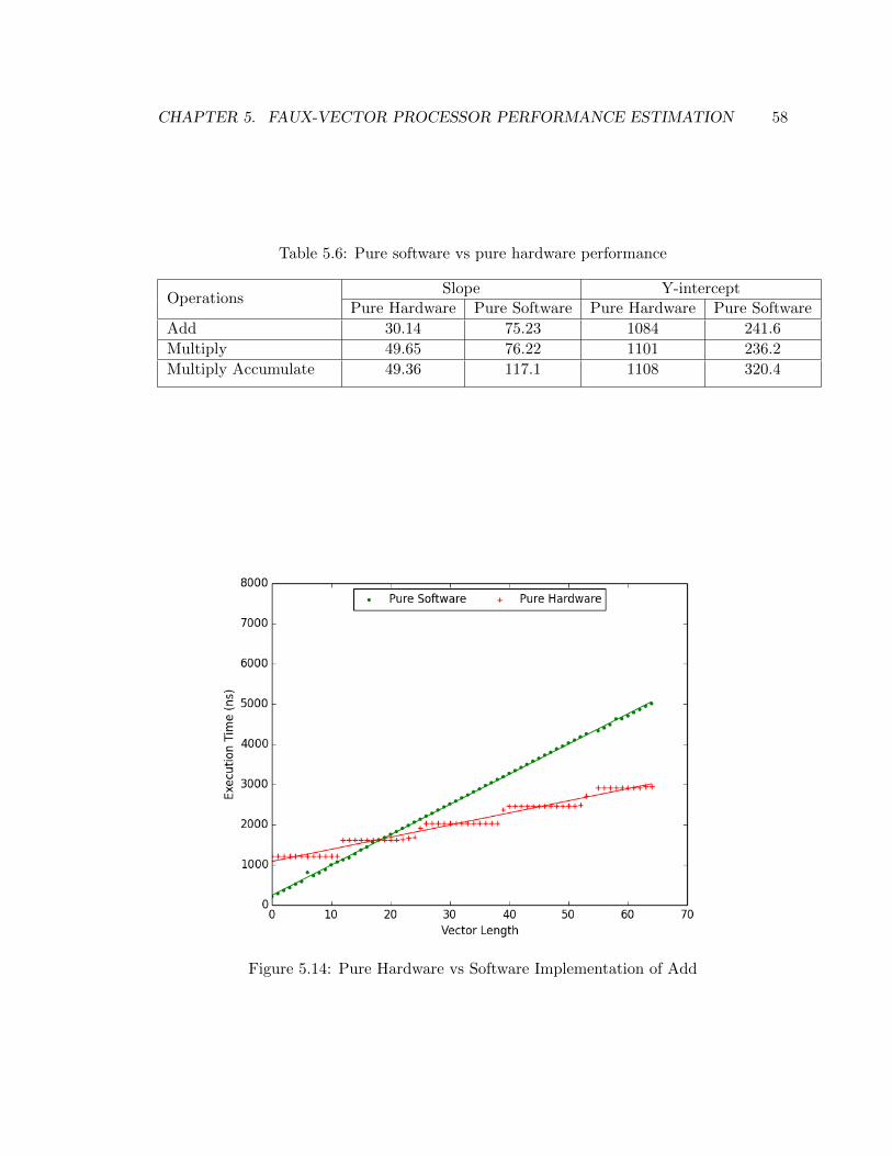
CHAPTER 5. FAUX-VECTOR PROCESSOR PERFORMANCE ESTIMATION 58
Table 5.6: Pure software vs pure hardware performance
Operations
Slope Y-intercept
Pure Hardware Pure Software Pure Hardware Pure Software
Add 30.14 75.23 1084 241.6
Multiply 49.65 76.22 1101 236.2
Multiply Accumulate 49.36 117.1 1108 320.4
Figure 5.14: Pure Hardware vs Software Implementation of Add
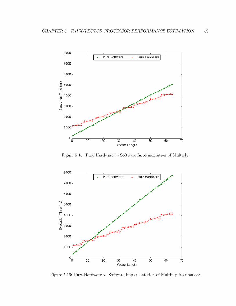
CHAPTER 5. FAUX-VECTOR PROCESSOR PERFORMANCE ESTIMATION 59
Figure 5.15: Pure Hardware vs Software Implementation of Multiply
Figure 5.16: Pure Hardware vs Software Implementation of Multiply Accumulate
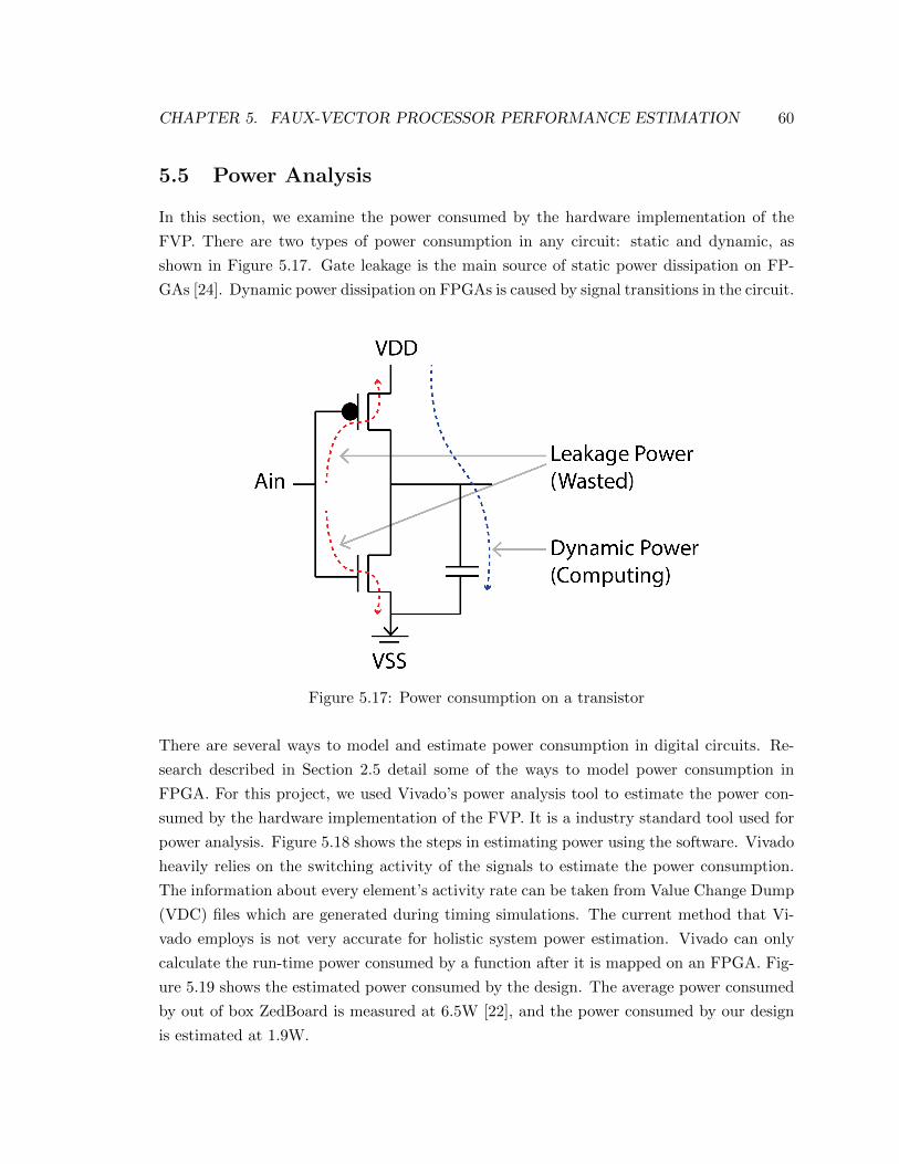
CHAPTER 5. FAUX-VECTOR PROCESSOR PERFORMANCE ESTIMATION 60
5.5 Power Analysis
In this section, we examine the power consumed by the hardware implementation of the
FVP. There are two types of power consumption in any circuit: static and dynamic, as
shown in Figure 5.17. Gate leakage is the main source of static power dissipation on FP-
GAs [24]. Dynamic power dissipation on FPGAs is caused by signal transitions in the circuit.
Figure 5.17: Power consumption on a transistor
There are several ways to model and estimate power consumption in digital circuits. Re-
search described in Section 2.5 detail some of the ways to model power consumption in
FPGA. For this project, we used Vivado’s power analysis tool to estimate the power con-
sumed by the hardware implementation of the FVP. It is a industry standard tool used for
power analysis. Figure 5.18 shows the steps in estimating power using the software. Vivado
heavily relies on the switching activity of the signals to estimate the power consumption.
The information about every element’s activity rate can be taken from Value Change Dump
(VDC) files which are generated during timing simulations. The current method that Vi-
vado employs is not very accurate for holistic system power estimation. Vivado can only
calculate the run-time power consumed by a function after it is mapped on an FPGA. Fig-
ure 5.19 shows the estimated power consumed by the design. The average power consumed
by out of box ZedBoard is measured at 6.5W [22], and the power consumed by our design
is estimated at 1.9W.
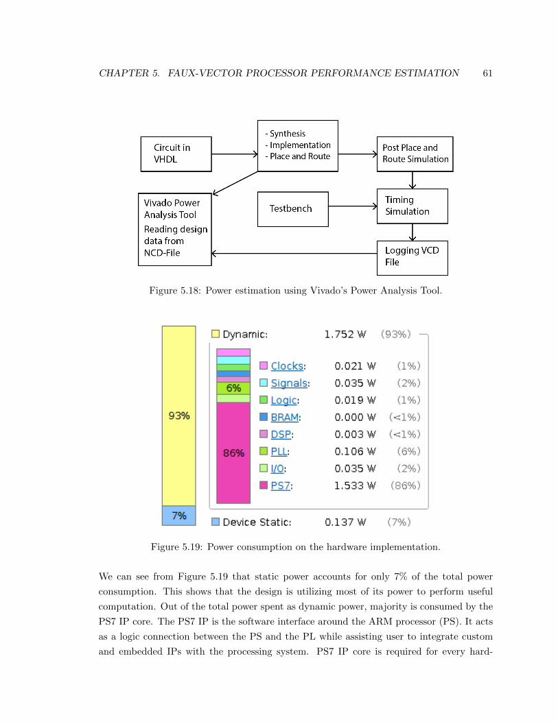
CHAPTER 5. FAUX-VECTOR PROCESSOR PERFORMANCE ESTIMATION 61
Figure 5.18: Power estimation using Vivado’s Power Analysis Tool.
Figure 5.19: Power consumption on the hardware implementation.
We can see from Figure 5.19 that static power accounts for only 7% of the total power
consumption. This shows that the design is utilizing most of its power to perform useful
computation. Out of the total power spent as dynamic power, majority is consumed by the
PS7 IP core. The PS7 IP is the software interface around the ARM processor (PS). It acts
as a logic connection between the PS and the PL while assisting user to integrate custom
and embedded IPs with the processing system. PS7 IP core is required for every hard-
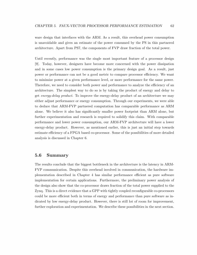
CHAPTER 5. FAUX-VECTOR PROCESSOR PERFORMANCE ESTIMATION 62
ware design that interfaces with the ARM. As a result, this overhead power consumption
is unavoidable and gives an estimate of the power consumed by the PS in this partnered
architecture. Apart from PS7, the components of FVP draw fraction of the total power.
Until recently, performance was the single most important feature of a processor design
[9]. Today, however, designers have become more concerned with the power dissipation
and in some cases low power consumption is the primary design goal. As a result, just
power or performance can not be a good metric to compare processor e�ciency. We want
to minimize power at a given performance level, or more performance for the same power.
Therefore, we need to consider both power and performance to analyze the e�ciency of an
architecture. The simplest way to do so is by taking the product of energy and delay to
get energy-delay product. To improve the energy-delay product of an architecture we may
either adjust performance or energy consumption. Through our experiments, we were able
to deduce that ARM-FVP partnered computation has comparable performance as ARM
alone. We believe it also has significantly smaller power footprint than ARM alone, but
further experimentation and research is required to solidify this claim. With comparable
performance and lower power consumption, our ARM-FVP architecture will have a lower
energy-delay product. However, as mentioned earlier, this is just an initial step towards
estimate e�ciency of a FPGA based co-processor. Some of the possibilities of more detailed
analysis is discussed in Chapter 6.
5.6 Summary
The results conclude that the biggest bottleneck in the architecture is the latency in ARM-
FVP communication. Despite this overhead involved in communication, the hardware im-
plementation described in Chapter 4 has similar performance e�cient as pure software
implementation for certain applications. Furthermore, the preliminary power analysis of
the design also show that the co-processor draws fraction of the total power supplied to the
Zynq. This is a direct evidence that a GPP with tightly coupled reconfigurable co-processors
could be more e�cient both in terms of energy and performance than pure software as in-
dicated by low energy-delay product. However, there is still lot of room for improvement,
further exploration and experimentation. We describe these possibilities in the next section.
6. Future Work
The FVP described in Chapter 4 is a first attempt to show the benefits of using a FPGA-
based co-processor system. In this section, we will discuss some of the ways to further
improve the FVP and techniques to measure its performance.
6.1 Improving Faux-Vector Processor Design
6.1.1 Upgrading Memory Interface Unit
The memory interface unit used for data transferring in our design is the primary bottle-
neck in performing any computation on the co-processor. In our current implementation
the synchronization time for performing any computation on the co-processor is about 1180
ns, which is significantly higher than performing any computation on a GPP itself. This
overhead is the main reason why the pure software implementation of the benchmark pro-
grams described in Section 5.4 is faster than than the hybrid implementation. There are
few ways to overcome this overhead limitation.
One approach is to implement data pipelining. Pipelining the data transfer would allow
computation to begin before all of the data had been read into the FPGA. Pipelining would
mitigate the overhead of data transfer by ensuring that after the first set of data had been
read, useful computation and not just data transfer would be done during all future transfer
cycles. Another approach to reduce the FPGA-host data latency is to make use of Direct
Memory Access (DMA) feature supported by many FPGAs. DMA is a FIFO-based method
of transferring data between FPGA and a host. The biggest advantage of using DMA is
that it doesn’t involve the host processor; therefore, it would free the host processor to
perform other useful computation during data transfer. As a result, it is faster than other
methods of transferring large amount of data. Furthermore, a DMA based approach is
optimized to save FPGA resources, and can also automatically synchronize data transfers
between the host and a FPGA. The Zynq system used in this project supports di↵erent
kind of DMA based data transfers, but the usage and properties of these DMA IP cores are
63
CHAPTER 6. FUTURE WORK 64
poorly documented.
Another alternative to reduce ARM-FVP communication latency is through instruction
pipelining. In the current version of our implementation, the FVP sits idle while the ARM
processor is executing instructions. As a consequence, we are not only wasting computa-
tional resource but also loosing power e�ciency. Therefore, instead of loading one instruc-
tion at a time, we could load multiple instructions at a time and only retrieve the results
after all the instructions are executed. This would hugely improve the e�ciency of our
architecture both in terms of power and performance by reducing power consumption and
latency from instruction synchronization.
6.1.2 Broadening the Functionality
The current implementation of faux vector processor is very limited in its scope. We cur-
rently support operations only on unsigned integers and the operations themselves are lim-
ited. Another way to make the FVP more capable would be to increase its scope. Adding
support for signed and floating point inputs would allow the vector processor to be used for
a much broader set of computation intensive tasks. Unlike other improvements, this would
be a trival extension as the co-processor is highly reconfigurable and our system is designed
in such a way that users can add more functionality very easily.
6.1.3 Multiple Lane Extension
The current version of FVP only supports single vector lane. As a result, all the computation
is performed sequentially. By performing computation sequentially, we are essentially losing
potential performance improvement by harnessing the power of parallelism. For the scope of
this project, we are focused on energy improvement rather than performance improvement.
This leads us to fix the number of lanes of the FVP to single lane. Possible extension to this
work could support multiple vector lanes and analyze both the power and performance of
such architecture. We believe that adding more vector lanes would definitely improve the
performance of the FVP, but it is hard to predict the magnitude of increase in the energy
consumption. Future work could possibly look at this performance-energy trade o↵.
6.1.4 Integration with a Vector Compiler
For a FPGA-based co-processor like FVP to gain widespread use, it must be integrated
into compilers. In the current implementation of our system, we are able to provide some
CHAPTER 6. FUTURE WORK 65
level of abstraction to the user through library calls. However, this still requires the user
to first translate their code into vector assembly motivated library calls. If this process is
automated by using a vector compiler to target our system, then it would not only provide
a higher level or abstraction and ease of use to the users but also increase performance. In
the current implementation, the user has to decide what operations are expensive to run on
the host processor and on the co-processor. After integrating our architecture with a vector
compiler, this process could be automated and compiler can make the decision at runtime
whether or not the co-processor should be invoked for a specific instance of a computation.
This would maximize e�ciency of both programmer and the co-processor.
6.1.5 Automating Circuit Design and Synthesis
As described in Section 3, the process of circuit design, synthesis, and implementation on
FPGA is involved. As a result, circuits for frequently used circuits could be automatically
generated, installed, and controlled by partial reconfigurable manager. In fact, the processor
could evaluate the performance of these circuits, improve their designs, and recompile them
into libraries. Over time, such an architecture would specialize each co-processor to its end
user without explicit inputs from the user. However, there is still a long way to go before we
could build such an architecture as the current state of art software used to program FPGAs
are very primitive. Improving these software to program FPGAs is crucial to reaching the
ultimate goal of automated circuit design and synthesis.
6.2 Improving Performance Estimation
6.2.1 Improved Power Analysis and Optimization
Power estimation is crucial in hardware devices as it is required to determine weather the
device will meet the targeted power specifications. Power analysis of the IP-based system
like Zynq is a particularly challenging task at the architecture level because the designers
need to compute accurate power estimates without direct knowledge of the IP design details.
Dynamic power consumption depends heavily on the design activity when in operation, but
many power estimation softwares, like Vivado’s power estimation tool, use simulation to
estimate the design activity. The problem with this approach is that simulation can mimic
the logic of the circuit, but cannot test how the logic will be implemented in the hard-
ware. In this project, we heavily relied on Vivado’s power analysis tool to estimate power
consumed by our co-processor. However, more detailed power analysis could be performed
by using both Vivado’s power analysis tool and the techniques from research described in
Chapter 2.
CHAPTER 6. FUTURE WORK 66
Furthermore, there are various power optimizations that could be performed in our faux
vector processor design. The current implementation of our design uses the memory inter-
face unit which is not optimized for power as both the FPGA and host has read line to the
shared memory constantly high. The architecture could be made more power e�cient by
switching to an interrupt-based system where FPGA and host communicate via interrupts
rather than by comparing instruction IDs.
6.3 Open Challenges
Because of these promising avenues of exploration, we expect the relevance of FPGAs in
computing systems to increase in the coming years. Leading market processor manufac-
turers like Intel are already moving towards integrated configurable logic with commodity
CPUs [11]. It is thus no longer a question whether or not FPGAs will appear in main-
stream computing systems. Rather, programming community should begin to worry about
how the potential of FPGAs can be leveraged to improve performance and energy e�ciency.
Several decades of research and development work have matured the software world to a
degree that virtually any application field receives a rich set of support by tools, program-
ming languages, libraries, design patterns and good practices. Hardware development, on
the other hand, is significantly more complex and has not yet reached the degree of con-
venience that software developers have long been used to. This is unfortunate not only
because potential of hardware technologies like FPGA hasn’t been fully realized, but also
because hardware-software co-design has, so far, been mostly ignored. Finding a system
architecture that brings together the potential of hardware and ease of software develop-
ment will require a fair amount of experimentation, design, and evaluation. The results
from our work are promising, but there is still lot of work to be done to improve the field
of hardware-software co-design before it can be attractive for practical use.
7. Conclusions
GPPs are designed for flexibility, with application performance and energy e�ciency only
as secondary goals. On the other hand, ASIC designs sacrifice flexibility for performance
and energy e�ciency. Designers of FPGA circuits, however, are not bound to this prioriti-
zation. Rather, their circuit typically has to support just one very specific application type
and the circuit can be rebuilt whenever it is no longer needed for the current application.
Given this freedom, the true potential of FPGA lies in the open space in-between flexibility
and e�ciency. Most likely, the sweet spot is when di↵erent processing units, composed
of one or more FPGA units; one or more general-purpose CPUs, operate together in the
some form of a hybrid system design. Our design with a dual core ARM processor tightly
coupled with a faux vector co-processor is a first step towards building such a hybrid system.
The co-processor design described in this work is capable of performing real-world appli-
cations. Our preliminary experiments have shown promising results indicating that such a
hybrid system would provide flexibility as well as performance and energy e�ciency to some
extent. Experiments described in Chapter 5 have shown that the bottleneck for a hybrid
FPGA-host architecture like ours is the data transfer mechanism. In Chapter 6 we provide
some suggestions to improve the data transfer mechanism, and also suggest possible paths
for future exploration. Basic energy analysis described in Chapter 5 using Vivado’s power
analysis tool has estimated that FPGA-based co-processor are e�cient at energy utilization
and consume only a small fraction of the total power supplied.
Our faux vector processor design and the future work discussed in Chapter 6 provides a first
successful attempt in creating a Zynq based FPGA-host hybrid architecture. By further
exploring this hardware-software co-design space, we will be able to design architectures
with GPP-like flexibility with ASIC-like e�ciency.
67

Acronyms
ALU arithmetic logic units (ALUs) are fundamental processor components that perform
arithmetic or bitwise logical functions on binary integer inputs.
ARM advanced RISC machine (ARM) is a set of RISC architectures developed by ARM
Holdings. ARM is currently the dominant RISC architecture, and ARM processors
are used in most mobile devices.
ASIC application specific integrated circuits (ASICs) are integrated circuits designed for
a particular application. They generally cannot be used for other purposes.
AXI Advanced eXtensible Interface (AXI) is a set of micro-controller buses used in the
Zynq SoC to handle data transfer between the PS and IP cores on the PL.
BRAM block RAMs that are placed on an FPGA fabric to provide more e�cient memory
storage for FPGA circuits.
CPU the central processing unit (CPU) performs the instructions of a computer program.
DSP Digital Signal Processor is an IP block in Zynq boards responsible of fast and e�cient
multiplication and addition.
FPGA field programmable gate arrays (FPGAs) are integrated circuits that can be recon-
figured after they have been manufactured.
FVP Faux vector processor is a vector processor that has single lane and executes opera-
tions sequentially rather than in parallel.
GPGPU general purpose computing on graphics processing units (GPGPU) refers to using
a GPU to execute computation normally performed by the CPU. GPGPU can have
better performance than computation on a CPU for applications with large amounts
of data parallelism, such as vector processing.
68
Acronyms 69
GPP general purpose processors (GPPs) are processors that can be used for a wide variety
of programs and applications.
GPU graphics processor units (GPUs) are integrated circuits designed to e�ciently process
images for output to a display. GPUs exploit data parallelism to achieve much higher
performance than CPUs for typical image processing algorithms.
IP intellectual property (IP) cores are how Xilinx defines the individual hardware blocks
that can be implemented on their FPGAs.
LUT look-up tables (LUTs) replace computation with indexing into a stored data array.
Most computation on FPGAs is implemented through select lines that index into
LUTs to encode boolean logic functions.
MIPS microprocessor without interlocked pipeline stages (MIPS) is a RISC instruction set
first introduced by MIPS Technologies in 1981.
PL Programmable Logic (PL) is Xilinx’s term for FPGA in their architecture.
PS Processing System (PS) is Xilinx’s term for ARM processor in their architecture.
RAM random access memory (RAM) is a type of data storage in which read and write
times are independent of order of access.
VHDL VHSIC Hardware Description Language (VHDL) is a hardware description lan-
guage used to define digital systems and integrated circuits. VHDL and Verilog are
the two most widely used hardware description languages.
VIRAM VIRAM is a vector extension of MIPS processor and stands for vector intelligent
RAM.
Bibliography
[1] Osama T Albaharna, Peter YK Cheung, and Thomas J Clarke. On the viability of
fpga-based integrated coprocessors. In FPGAs for Custom Computing Machines, 1996.
Proceedings. IEEE Symposium on, pages 206–215. IEEE, 1996.
[2] Andrew Canis, Jongsok Choi, Mark Aldham, Victor Zhang, Ahmed Kammoona, Ja-
son H Anderson, Stephen Brown, and Tomasz Czajkowski. Legup: high-level synthesis
for fpga-based processor/accelerator systems. In Proceedings of the 19th ACM/SIGDA
international symposium on Field programmable gate arrays, pages 33–36. ACM, 2011.
[3] Andrew Canis, Jongsok Choi, Mark Aldham, Victor Zhang, Ahmed Kammoona,
Tomasz Czajkowski, Stephen D Brown, and Jason H Anderson. Legup: An open-
source high-level synthesis tool for fpga-based processor/accelerator systems. ACM
Transactions on Embedded Computing Systems (TECS), 13(2):24, 2013.
[4] Eric S. Chung, Peter A. Milder, James C. Hoe, and Ken Mai. Single-chip hetero-
geneous computing: Does the future include custom logic, FPGAs, and GPGPUs?
In Proceedings of the 2010 43rd Annual IEEE/ACM International Symposium on
Microarchitecture, MICRO ’43, pages 225–236, Washington, DC, USA, 2010. IEEE
Computer Society. ISBN 978-0-7695-4299-7. doi: 10.1109/MICRO.2010.36. URL
http://dx.doi.org/10.1109/MICRO.2010.36.
[5] Silviu Ciricescu, Ray Essick, Brian Lucas, Phil May, Kent Moat, Jim Norris, Michael
Schuette, and Ali Saidi. The reconfigurable streaming vector processor (rsvptm). In
Proceedings of the 36th annual IEEE/ACM International Symposium on Microarchi-
tecture, page 141. IEEE Computer Society, 2003.
[6] Vijay Degalahal and Tim Tuan. Methodology for high level estimation of fpga power
consumption. In Proceedings of the 2005 Asia and South Pacific Design Automation
Conference, pages 657–660. ACM, 2005.
[7] Robert H Dennard, VL Rideout, E Bassous, and AR LeBlanc. Design of ion-implanted
70
BIBLIOGRAPHY 71
mosfet’s with very small physical dimensions. Solid-State Circuits, IEEE Journal of, 9
(5):256–268, 1974.
[8] Shane T Fleming, Ivan Beretta, David B Thomas, George A Constantinides, and Dan R
Ghica. Pushpush: Seamless integration of hardware and software objects via function
calls over axi. In Field Programmable Logic and Applications (FPL), 2015 25th Inter-
national Conference on, pages 1–8. IEEE, 2015.
[9] Ricardo Gonzalez and Mark Horowitz. Energy dissipation in general purpose micro-
processors. Solid-State Circuits, IEEE Journal of, 31(9):1277–1284, 1996.
[10] N. Goulding-Hotta, J. Sampson, G. Venkatesh, S. Garcia, J. Auricchio, P. Huang,
M. Arora, S. Nath, V. Bhatt, J. Babb, S. Swanson, and M. Taylor. The GreenDroid
mobile application processor: An architecture for silicon’s dark future. Micro, IEEE,
31(2):86–95, March 2011. ISSN 0272-1732. doi: 10.1109/MM.2011.18.
[11] Prabhat K Gupta. Xeon+ fpga platform for the data center. In Fourth Workshop
on the Intersections of Computer Architecture and Reconfigurable Logic, volume 119,
2015.
[12] Rehan Hameed, Wajahat Qadeer, Megan Wachs, Omid Azizi, Alex Solomatnikov, Ben-
jamin C. Lee, Stephen Richardson, Christos Kozyrakis, and Mark Horowitz. Under-
standing sources of ine�ciency in general-purpose chips. SIGARCH Comput. Archit.
News, 38(3):37–47, June 2010. ISSN 0163-5964. doi: 10.1145/1816038.1815968. URL
http://doi.acm.org/10.1145/1816038.1815968.
[13] Mark D Hill and Michael R Marty. Amdahl’s Law in the multicore era. IEEE Computer,
41(7):33–38, 2008.
[14] Matthew Jacobsen and Ryan Kastner. Ri↵a 2.0: A reusable integration framework
for fpga accelerators. In Field Programmable Logic and Applications (FPL), 2013 23rd
International Conference on, pages 1–8. IEEE, 2013.
[15] Ruzica Jevtic and Carlos Carreras. Power measurement methodology for fpga devices.
Instrumentation and Measurement, IEEE Transactions on, 60(1):237–247, 2011.
[16] Myron King, Jamey Hicks, and John Ankcorn. Software-driven hardware develop-
ment. In Proceedings of the 2015 ACM/SIGDA International Symposium on Field-
Programmable Gate Arrays, pages 13–22. ACM, 2015.
[17] Christoforos Kozyrakis and David A Patterson. Scalable vector media-processors for
embedded systems. University of California, Berkeley, 2002.
BIBLIOGRAPHY 72
[18] Christos Kozyrakis and David Patterson. Overcoming the limitations of conventional
vector processors. In ACM SIGARCH Computer Architecture News, volume 31, pages
399–409. ACM, 2003.
[19] Ian Kuon and Jonathan Rose. Measuring the gap between FPGAs and ASICs.
Computer-Aided Design of Integrated Circuits and Systems, IEEE Transactions on,
26(2):203–215, 2007.
[20] Chris Lattner and Vikram Adve. Llvm: A compilation framework for lifelong program
analysis & transformation. In Code Generation and Optimization, 2004. CGO 2004.
International Symposium on, pages 75–86. IEEE, 2004.
[21] David Martin. Vector Extensions to the MIPS-IV Instruction Set Architecture. 2000.
[22] Josh Monson, Michael Wirthlin, and Brad L Hutchings. Implementing high-
performance, low-power fpga-based optical flow accelerators in c. In Application-
Specific Systems, Architectures and Processors (ASAP), 2013 IEEE 24th International
Conference on, pages 363–369. IEEE, 2013.
[23] Chuck Moore. Data processing in exascale-class computer systems. In The Salishan
Conference on High Speed Computing, 2011.
[24] Li Shang, Alireza S Kaviani, and Kusuma Bathala. Dynamic power consumption in
virtex
TM-ii fpga family. In Proceedings of the 2002 ACM/SIGDA tenth international
symposium on Field-programmable gate arrays, pages 157–164. ACM, 2002.
[25] David B Thomas, Shane T Fleming, George A Constantinides, and Dan R Ghica.
Transparent linking of compiled software and synthesized hardware. In Proceedings
of the 2015 Design, Automation & Test in Europe Conference & Exhibition, pages
1084–1089. EDA Consortium, 2015.
[26] Tim Tuan and Bocheng Lai. Leakage power analysis of a 90nm fpga. In Custom In-
tegrated Circuits Conference, 2003. Proceedings of the IEEE 2003, pages 57–60. IEEE,
2003.
[27] Ganesh Venkatesh, Jack Sampson, Nathan Goulding, Saturnino Garcia, Vladyslav
Bryksin, Jose Lugo-Martinez, Steven Swanson, and Michael Bedford Taylor. Conserva-
tion Cores: Reducing the energy of mature computations. SIGARCH Comput. Archit.
News, 38(1):205–218, March 2010. ISSN 0163-5964. doi: 10.1145/1735970.1736044.
URL http://doi.acm.org/10.1145/1735970.1736044.
BIBLIOGRAPHY 73
[28] Ganesh Venkatesh, Jack Sampson, Nathan Goulding-Hotta, Sravanthi Kota Venkata,
Michael Bedford Taylor, and Steven Swanson. QsCores: Trading dark silicon for
scalable energy e�ciency with quasi-specific cores. In Proceedings of the 44th An-
nual IEEE/ACM International Symposium on Microarchitecture, MICRO-44, pages
163–174, New York, NY, USA, 2011. ACM. ISBN 978-1-4503-1053-6. doi:
10.1145/2155620.2155640. URL http://doi.acm.org/10.1145/2155620.2155640.
[29] Dong Hyuk Woo and Hsien-Hsin S Lee. Extending amdahl’s law for energy-e�cient
computing in the many-core era. Computer, (12):24–31, 2008.
[30] UG585. Zynq-7000 All Programmable SoC. Xilinx, v1.8.1 edition, Sept 2014.
[31] Xillybus. URL http://xillybus.com/.
[32] Peter Yiannacouras, J Gregory Ste↵an, and Jonathan Rose. Portable, flexible, and
scalable soft vector processors. Very Large Scale Integration (VLSI) Systems, IEEE
Transactions on, 20(8):1429–1442, 2012.
[33] Jason Yu. Architecture Specification for Vector Extension to Nios II ISA. 2008.
[34] Jason Yu, Guy Lemieux, and Christpher Eagleston. Vector processing as a soft-core
cpu accelerator. In Proceedings of the 16th international ACM/SIGDA symposium on
Field programmable gate arrays, pages 222–232. ACM, 2008.
[35] Zedboard. URL http://zedboard.org/.