features and benefits - maxim integratedfeatures and benefits high-accuracy flow measurement for...
TRANSCRIPT

General DescriptionThe MAX35102 is a time-to-digital converter with built-in amplifier and comparator targeted as a low-cost, analog front-end solution for the ultrasonic heat meter and flow meter markets. It is similar to the MAX35101, but with a reduced feature set and without a real-time clock (RTC). The package size has been reduced to 4mm x 4mm x 0.75mm with 0.4mm pin pitch.With a time measurement accuracy of 20ps and auto-matic differential time-of-flight (ToF) measurement, this device makes for simplified computation of liquid flow.Power consumption is the lowest available with ultra-low 5.5μA ToF measurement and < 125nA duty-cycled tem-perature measurement.
Applications Ultrasonic Heat Meters Ultrasonic Water Meters Ultrasonic Gas Meters
Features and Benefits High-Accuracy Flow Measurement for Billing and
Leak Detection• Time-to-Digital Accuracy Down to 20ps• Measurement Range Up to 8ms• 2 Channels—Single-Stop Channel
High-Accuracy Temperature Measurement for Precise Heat and Flow Calculations• Up to Four 2-Wire Sensors• PT1000 and PT500 RTD Support• 40mK Accuracy
Maximizes Battery Life with Low Device and Overall System Power• Ultra-Low 5.5μA ToF measurement and < 125nA
Duty-Cycled Temperature Measurement• 2.3V to 3.6V Single-Supply Operation
High-Integration Solution Minimizes Parts Count and Reduces BOM Cost• Small, 4mm x 4mm, 32-Pin TQFN Package• -40°C to +85°C OperationOrdering Information appears at end of data sheet.
MICROCONTROLLER
32.768 KHZ4 MHZ
PT 1000
PT 1000
1K (50 PPM) METAL FILM
100 NF COG (NP0) (30 PPM/C)
PIEZOELECTRIC TRANSDUCERS
3.6 V
100 NF LOW ESR
12 PF12 PF12 PF
12 PF
TIME-TO-DIGITAL CONVERTER PROGRAMMABLE ALU
DATA AND STATUS
REGISTERS
CONFIGURATION REGISTERS
STP_UP
STP_DN
STATE MACHINE CONTROLLER
PULSE LAUNCHER
LAUNCH_UP
LAUNCH_DN
T1
TEMPERATURE MEASUREMENTHIGH SPEED AND 32 KHZ OSCILLATORS
X1 X2 32KX1 32KXO 32KOUT
4-WIREINTERFACE
SCK
DIN
DOUT
CEX
INTX
RSTX
CMP_OUT/UP_DN GND
T4T2 T3 TC
ANALOG SWITCHING AND BIAS CONTROL
VCC
BYPASSINTERNAL
LDO
MAX35102 Time-to-Digital Converter Without RTC
19-7442; Rev 0; 11/14
System Block Diagram
EVALUATION KIT AVAILABLE

(Voltages relative to ground.)Voltage Range on VCC Pins.................................-0.5V to +4.0VVoltage Range on All Other Pins
(not to exceed 4.0V) ............................. -0.5V to (VCC + 0.5V)Continuous Power Dissipation (TA = +70°C) TQFN (derate 29.40mW/ºC above +70°C) ...........2352.90mW
Operating Temperature Range ........................... -40°C to +85°CJunction Temperature ......................................................+150°CStorage Temperature Range ............................ -55°C to +125°CLead Temperature (soldering, 10s) .................................+300°CSoldering Temperature (reflow) .......................................+260°CESD Protection (All Pins, Human Body Model) ..................±2kV
TQFN Junction-to-Ambient Thermal Resistance (θJA) ..........34°C/W Junction-to-Case Thermal Resistance (θJC) .....................3°C/W
(Note 1)
(VCC = 2.3V to 3.6V, TA = -40°C to +85°C, unless otherwise noted. Typical values are at VCC = 3.0V and TA = +25°C.) (Notes 2, 3)
(TA = -40°C to +85°C, unless otherwise noted.) (Notes 2, 3)
PARAMETER SYMBOL CONDITIONS MIN TYP MAX UNITS
Supply Voltage VCC 2.3 3.0 3.6 V
Input Logic 1 (RST, SCK, DIN, CE) VIH VCC x 0.7 VCC + 0.3 V
Input Logic 0 (RST, SCK, DIN, CE) VIL -0.3 VCC x 0.3 V
Input Logic 1 (32KX1) VIH32KX1 VCC x 0.85 VCC + 0.3 V
Input Logic 0 (32KX1) VIL32KX1 -0.3 VCC x 0.15 V
PARAMETER SYMBOL CONDITIONS MIN TYP MAX UNITSInput Leakage (RST, SCK, DIN, CE) IL -0.1 +0.1 µA
Output Leakage (INT, T1,T2,T3,T4) OL -0.1 +0.1 µA
Output Voltage Low (32KOUT) VOL32K 2mA 0.2 x VCC V
Output Voltage High (32KOUT) VOH32K -1mA 0.8 x VCC V
Output Voltage High (DOUT, CMP_OUT/UP_DN) VOH -4mA 0.8 x VCC V
Output Voltage High (TC) VOHTC VCC = 3.3V, IOUT = -4mA 2.9 3.1 V
Output Voltage High (Launch_UP, Launch_DN) VOHLAUCH VCC = 3.3V, IOUT = -50mA 2.8 3.0 V
Output Voltage Low (INT, DOUT, CMP_OUT/UP_DN) VOL 4mA 0.2 x VCC V
MAX35102 Time-to-Digital Converter Without RTC
www.maximintegrated.com Maxim Integrated 2
Note 1: Package thermal resistances were obtained using the method described in JEDEC specification JESD51-7, using a four-layer board. For detailed information on package thermal considerations, refer to www.maximintegrated.com/thermal-tutorial.
Absolute Maximum Ratings
Stresses beyond those listed under “Absolute Maximum Ratings” may cause permanent damage to the device. These are stress ratings only, and functional operation of the device at these or any other conditions beyond those indicated in the operational sections of the specifications is not implied. Exposure to absolute maximum rating conditions for extended periods may affect device reliability.
Package Thermal Characteristics
Electrical Characteristics
Recommended Operating Conditions

(VCC = 2.3V to 3.6V, TA = -40°C to +85°C, unless otherwise noted. Typical values are at VCC = 3.0V and TA = +25°C.) (Notes 2, 3)
PARAMETER SYMBOL CONDITIONS MIN TYP MAX UNITS
Pulldown Resistance (TC) RTC 650 1000 1500 Ω
Input Voltage Low (TC) VILTC 0.36 x VCC V
Output Voltage Low (Launch_UP, Launch_DN) VOLLAUCH VCC = 3.3V, IOUT = 50mA 0.2 0.4 V
Resistance (T1, T2, T3, T4) RON 1 Ω
Input Capacitance (CE, SCK, DIN, RST) CIN Not tested 7 pF
RST Low Time tRST 100 ns
CURRENT
Standby Current IDDQ No oscillators running, TA = +25°C 0.1 1 µA
32kHz OSC Current I32KHZ 32kHz oscillator only (Note 4) 0.5 0.9 µA
4MHz OSC Current I4MHZ 4MHz oscillator only (Note 4) 40 85 µA
LDO Bias Current ICCLDO ICCCPU = 0 (Note 4) 15 50 µA
Time Measurement Unit Current ICCTMU (Note 4) 4.5 8 mA
Calculator Current ICCCPU 0.75 1.7 mA
Device Current Drain ICC3TOF_DIFF = 2 per second (3 hits), temperature = 1 per 30s 5.5 µA
ANALOG RECEIVER
Analog Input Voltage(STOP_UP, STOP_DN) VANA 10 700
2 x VCC x (3/8)
mVP-P
Input Offset Step Size VSTEP 1 mV
STOP_UP/STOP_DN Bias Voltage VBIAS VCC x (3/8) V
Receiver Sensitivity VANA Stop hit detect level (Note 5) 10 mVP-P
TIME MEASUREMENT UNIT
Measurement Range tMEAS Time of flight 8 8000 µs
Time Measurement Accuracy tACC Differential time measurement 20 ps
Time Measurement Resolution tRES 3.8 ps
EXECUTION TIMES
Power-On-Reset Time tRESET Reset to POR INT 275 µs
INIT Command Time tINIT Command received when INIT bit set 2.5 ms
CAL Command Time tCAL Command received when CAL bit set 1.25 ms
MAX35102 Time-to-Digital Converter Without RTC
www.maximintegrated.com Maxim Integrated 3
Electrical Characteristics (continued)

Note 2: All voltages are referenced to ground. Current entering the device are specified as positive and currents exiting the device are negative.
Note 3: Limits are 100% production tested at TA = +25°C. Limits over the operating temperature range and relevant supply voltage range are guaranteed by design and characterization.
Note 4: Currents are specified as individual block currents. Total current for a point in time can be calculated by taking the standby current and adding any block currents that are active at that time.
Note 5: Receiver sensitivity includes performance degradation contributed by STOP_UP and STOP_DN device pin input offset volt-age and common mode drift.
PARAMETER SYMBOL CONDITIONS MIN TYP MAX UNITS
32kHz Nominal Frequency f32K 32.768 kHz
32kHz Frequency Tolerance Δf32K/f32K TA = +25°C -20 +20 ppm
32kHz Load Capacitance CL32K 12.5 pF
32kHz Series Resistance RS32K 70 kΩ
4MHz Crystal Nominal Frequency F4M 4.000 MHz
4MHz Crystal Frequency Tolerance Δf4M/f4M TA = +25°C -30 +30 ppm
4MHz Crystal Load Capacitance CL4M 12.0 pF
4MHz Crystal Series Resistance RS4M 120 Ω
4MHz Ceramic Nominal Frequency 4.000 MHz
4MHz Ceramic Frequency Tolerance TA = +25°C -0.5 +0.5 %
4MHz Ceramic Load Capacitance 30 pF
4MHz Ceramic Series Resistance 30 Ω
PARAMETER SYMBOL CONDITIONS MIN TYP MAX UNITS
SERIAL PERIPHERAL INTERFACE
DIN to SCK Setup tDC 20 ns
SCK to DIN Hold tCDH 2 20 ns
SCK to DOUT Delay tCDD 5 20 ns
SCK Low Time tCLVCC ≥ 3.0V 25 4
nsVCC = 2.3V 50 30
SCK High Time tCH 25 4 ns
SCK Frequency tCLKVCC ≥ 3.0V 20
MHzVCC = 2.3V 10
CE to SCK Setup tCC 5 40 ns
SCK to CE Hold tCCH 20 ns
CE Inactive Time tCWH 2 40 ns
CE to DOUT High Impedance tCCZ 5 20 ns
MAX35102 Time-to-Digital Converter Without RTC
www.maximintegrated.com Maxim Integrated 4
Recommended External Crystal Characteristics
(VCC = 2.3V to 3.6V, TA = -40°C to +85°C, unless otherwise noted. Typical values are at VCC = 3.0V and TA = +25°C.) (Notes 2, 3)Electrical Characteristics (continued)

Figure 1. SPI Timing Diagram Read
Figure 2. SPI Timing Diagram Write
DOUTHIGH IMPEDANCE MSB LSB
tCDD tCCZ
CE
SCK
DIN
tCC
tDC
tCDH
tCWH
MSB LSB
Figure 1
CE
SCK
DIN
tCC
tDC
tCDH
tCL
tCHtCCH
tCWH
tR
tF
VIH
VIL
MSB
DOUT HIGH IMPEDANCE
tCLK
LSB
Figure 2
MAX35102 Time-to-Digital Converter Without RTC
www.maximintegrated.com Maxim Integrated 5
Timing Diagrams

(VCC = 3.3V and TA = +25°C, unless otherwise noted.)
22
24
26
28
30
32
34
-10 15 40 65 90ER
ROR
(ns)
TEMPERATURE (ºC)
ABSOLUTE ToF ERRORvs. TEMPERATURE toc02
0
5
10
15
20
25
30
35
40
45
0 5 10 15 20
AVER
AGE
ICC
(µA)
ToF MEASUREMENT RATE (TOFDIFF/s)
3 HITS
AVERAGE ICC vs. ToF RATEtoc03
22
24
26
28
30
32
34
2.20 2.45 2.70 2.95 3.20 3.45 3.70 3.95
ERRO
R (n
s)
VCC (V)
ABSOLUTE ToF ERRORvs. SUPPLY VOLTAGE toc01
VALUE BIT SETTINGSClock Settling Time 488µs CLK_S[2:0] = 000Bias Charge Time 61µs CT[1:0] = 00Pulse Launch Frequency 1MHz DPL[3:0] = 0001Pulse Launcher Size 15 PL[7:0] = 00001111TOF Duty Cycle 19.97ms TOF_CYC[2:0] = 111Stop Hits 3 STOP[1:0] = 010T2 Wave Selector Wave 2 T2WV[5:0] = 000110Temperature Port Number 4 TP[1:0] = 11Preamble Temperature Cycle Number 1 PRECYC[2:0] = 001Port Cycle Time 256µs PORTCYC[1:0] = 01
Notes1. This data is valid for the ceramic resonator.2. Crystal oscillator startup adds ~0.5µA per TOFDiff.3. Since the TOF cycle time is long the 4MHz oscillator powers up twice.
3 HIT SETTINGSCONTOL BIT(S)
Average ICC vs. TOF Rate Configuration Settings
MAX35102 Time-to-Digital Converter Without RTC
www.maximintegrated.com Maxim Integrated 6
Typical Operating Characteristics

PIN NAME FUNCTION
1, 16, 22, 25, 28, 30 GND Device Ground
2 BYPASS Connect this pin to ground with a capacitor (100nF) to provide stability for the on-board low-dropout regulator. The effective series resistance of this capacitor needs to be in the 1Ω to 2Ω range.
3, 6, 29 VCC Main Supply. Typically sourced from a single lithium cell.
4 32KOUT CMOS Output. Repeats the 32kHz crystal oscillator frequency.
5 LAUNCH_DN CMOS Pulse Output Transmission in Downstream Direction of Water Flow
7 LAUNCH _UP CMOS Pulse Output Transmission in Upstream Direction of Water Flow
8 CMP_OUT/UP_DN CMOS Output. Indicates the direction (upstream or downstream) of which the pulse launcher is currently launching pulses OR the comparator output.
9 INT Active-Low Open-Drain Interrupt Output. The pin is driven low when the device requires service from the host microprocessor.
10 CE Active-Low CMOS Digital Input. Serial peripheral interface chip enable input.
MAX35102
TQFN4mm x 4mm
TOP VIEW
BYPA
SS
32KO
UT
LAUN
CH_D
N
V CC
LAUN
CH_U
P
GND
32KX
0
TC T432KX
1
T3 T21 2
GND
4 5 6 7
VCC
GND
RST
DOUT
DIN
SCKV C
CGN
D
3
X2 CE
X1 INT+
STOP_UP
DNCSTOP_DN
GND
CMP_
OUT/
UP_D
NT1
8
GND 16
15
14
13
12
11
10
9
1718192021222324
26
25
27
28
29
30
31
32
MAX35102 Time-to-Digital Converter Without RTC
www.maximintegrated.com Maxim Integrated 7
Pin Description
Pin Configuration

PIN NAME FUNCTION
11 SCK CMOS Digital Input. Serial peripheral interface clock input.
12 DIN CMOS Digital Input. Serial peripheral interface data input.
13 DOUT CMOS Output. Serial peripheral interface data output.
14 RST Active-Low CMOS Digital Reset Input
15 DNC Do Not Connect. This pin must be left unconnected.
17 T1 Open-Drain Probe 1 Temperature Measurement
18 T2 Open-Drain Probe 2 Temperature Measurement
19 T3 Open-Drain Probe 3 Temperature Measurement
20 T4 Open-Drain Probe 4 Temperature Measurement
21 TC Input/Output Temperature Measurement Capacitor Connection
23 32KX0 Connections for 32.768kHz Quartz Crystal. An external CMOS 32.768kHz oscillator can also drive the MAX35102. In this configuration, the 32KX1 pin is connected to the external oscillator signal and the 32KX0 pin is left unconnected.24 32KX1
26 STOP_DN Downstream STOP Analog Input. Used for the signal that is received from the downstream transmission of a time-of-flight measurement.
27 STOP_UP Upstream STOP Analog Input. Used for the signal that is received from the upstream transmission of a time-of-flight measurement.
31 X2Connections for 4MHz Quartz Crystal. A ceramic resonator can also be used.
32 X1
— EP Exposed Pad. Connect to GND.
MAX35102 Time-to-Digital Converter Without RTC
www.maximintegrated.com Maxim Integrated 8
Pin Description (continued)
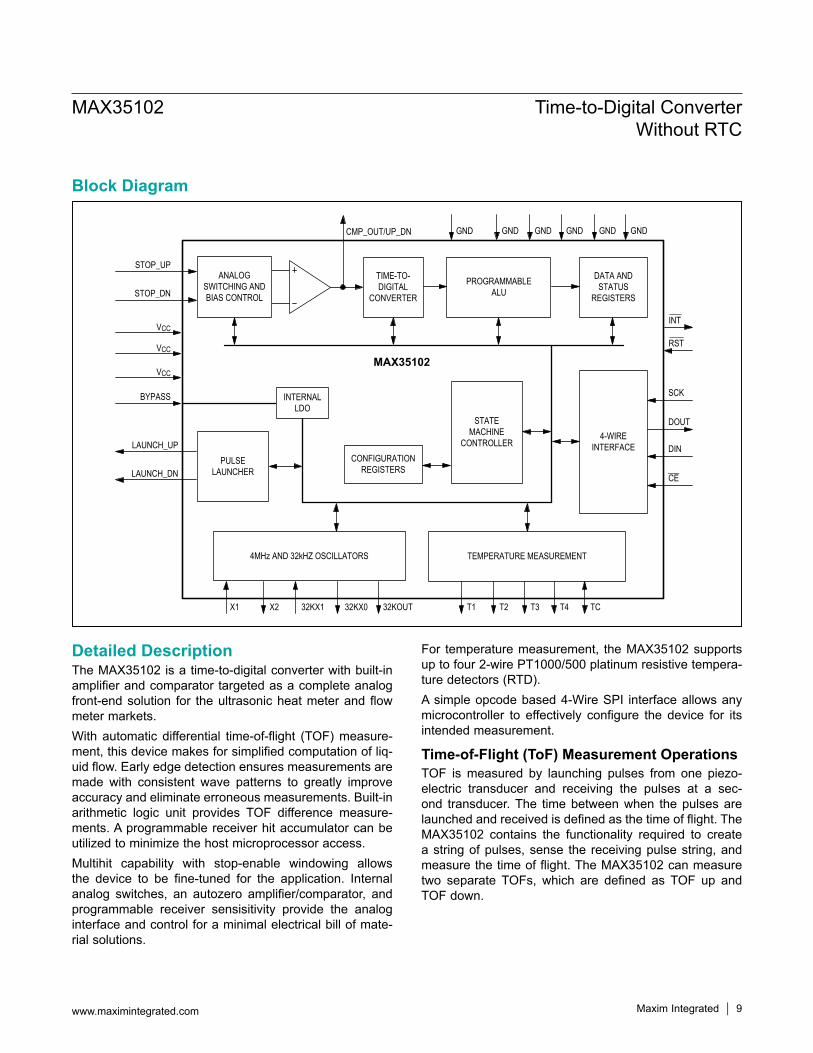
Detailed DescriptionThe MAX35102 is a time-to-digital converter with built-in amplifier and comparator targeted as a complete analog front-end solution for the ultrasonic heat meter and flow meter markets. With automatic differential time-of-flight (TOF) measure-ment, this device makes for simplified computation of liq-uid flow. Early edge detection ensures measurements are made with consistent wave patterns to greatly improve accuracy and eliminate erroneous measurements. Built-in arithmetic logic unit provides TOF difference measure-ments. A programmable receiver hit accumulator can be utilized to minimize the host microprocessor access.Multihit capability with stop-enable windowing allows the device to be fine-tuned for the application. Internal analog switches, an autozero amplifier/comparator, and programmable receiver sensisitivity provide the analog interface and control for a minimal electrical bill of mate-rial solutions.
For temperature measurement, the MAX35102 supports up to four 2-wire PT1000/500 platinum resistive tempera-ture detectors (RTD).A simple opcode based 4-Wire SPI interface allows any microcontroller to effectively configure the device for its intended measurement.
Time-of-Flight (ToF) Measurement OperationsTOF is measured by launching pulses from one piezo-electric transducer and receiving the pulses at a sec-ond transducer. The time between when the pulses are launched and received is defined as the time of flight. The MAX35102 contains the functionality required to create a string of pulses, sense the receiving pulse string, and measure the time of flight. The MAX35102 can measure two separate TOFs, which are defined as TOF up and TOF down.
TIME-TO-DIGITAL
CONVERTER
PROGRAMMABLEALU
DATA AND STATUS
REGISTERS
STATE MACHINE
CONTROLLER
PULSE LAUNCHER
STOP_UP
TEMPERATURE MEASUREMENT4MHz AND 32kHZ OSCILLATORS
X1
4-WIREINTERFACE
CMP_OUT/UP_DN
ANALOG SWITCHING AND BIAS CONTROL
INTERNAL LDO
MAX35102
STOP_DN
VCC
VCC
VCC
BYPASS
LAUNCH_UP
LAUNCH_DN
GND GND GND GND GND
CONFIGURATION REGISTERS
INT
RST
SCK
DOUT
DIN
CE
X2 32KX1 32KOUT32KX0 T1 T2 T3 T4 TC
GND
MAX35102 Time-to-Digital Converter Without RTC
www.maximintegrated.com Maxim Integrated 9
Block Diagram

A TOF up measurement has pulses launched from the LAUNCH_UP pin, which is connected to the downstream transducer. The ultrasonic pulse is received at the upstream transducer, which is connected to the STOP_UP pin. A TOF down measurement has pulses launched from the LAUNCH_DN pin, which is connected to the upstream transducer. The ultrasonic pulse is received at the downstream transducer, which is connected to the STOP_DN pin. TOF measurements can be initiated by sending either the TOF_UP, TOF_DN, or TOF_DIFF commands.The steps involved in a single TOF measurement are described here and shown in Figure 3.1) The 4MHz oscillator and LDO is enabled with a pro-
grammable settling delay time set by the CLK_S[2:0] bits in Calibration and Control register.
2) A common-mode bias is enabled on the STOP pin. This bias charge time is set by the CT[1:0] bits in the TOF1 register.
3) Once the bias charge time has expired, the pulse launcher drives the appropriate LAUNCH pin with a programmable sequence of pulses. The number of pulses launched is set by the PL[7:0] bits in the TOF1 register. The frequency of these 50% duty-cycle pulses is set by the DPL[3:0] bits, also in the TOF1 register. The start of these launch pulses gen-
erates a start signal for the time-to-digital converter (TDC) and is considered to be time zero for the TOF measurement. This is denoted by the start signal in the start/stop TDC timing (Figure 3).
4) After a programmable delay time set in TOF Measurement Delay register, the comparator and hit detector at the appropriate STOP pin are enabled. This delay allows the receiver to start recording hits when the received wave is expected, eliminating possible false hits from noise in the system.
5) Stop hits are detected according to the programmed preferred edge of the acoustic signal sequence received at the STOP pin according to the setting of the STOP_POL bit in the TOF1 register. The first stop hit is detected when a wave received at the STOP pin exceeds the comparator offset voltage, which is set in the TOF6 and TOF7 registers. This first detected wave is wave number 0. The width of the wave’s pulse that exceeds the comparator offset voltage is measured and stored as the t1 time.
6) The offset of the comparator then automatically and immediately switches to 0.
7) The t2 wave is detected and the width of the t2 pulse is measured and stored as the t2 time. The wave number for the measurement of the t2 wave width is set by the T2WV[5:0] bits in the TOF2 register.
Figure 3. Time-of-Flight Sequence
Figure 3
T1 HIT1
(2)BIAS APPLIED TO STOP PIN
(3)LAUNCH PULSES
ToF START
(5)T1 WAVE
(6)COMPARE RETURN
(7)T2
WAVE
HIT2
HIT3
(8)STOP HITS
(9)CALCULATIONS
ToF COMMAND RECEIVED
(1) 4 MHZ
STARTUP
LAUNCH PIN
STOP PIN
COMPARATOR OFFSETCOMPARATOR OFFSET FORCED TO 0
TIME OF FLIGHT MEASUREMENTS
WAVE NUMBER 765431 20
ToF MEASUREMENT SEQUENCE
STOP HITS SELECTED = 3, STOP POLARITY = POSITIVE EDGE
AVG = ∑(HIT[1:3]) ÷ 3
SELECTED WAVES FOR HITS:T2 = 4 HIT1 = 5 HIT2 = 6 HIT3 = 7
(4)ENABLE
RECEIVER
(10) INT
ASSERTED
T2
INT PIN
MAX35102 Time-to-Digital Converter Without RTC
www.maximintegrated.com Maxim Integrated 10

8) Following the t2 wave, 1 to 3 consecutive stop hits are then detected. For each hit, the measured TOF is stored in the appropriate HITxUPINT and HITxUPFrac or HITxDNINT and HITxDNFRAC reg-isters. The number of hits to detect is set by the STOP[1:0] bits in the TOF2 register.
9) After receiving all of the programmed hits, the MAX35102 calculates the average of the recorded hits and stores this to AVGUPINT and AVGUPFrac or AVGDNInt and AVGDNFrac. The ratio of t1/t2 and t2/tideal are calculated and stored in the WVRUP or WVRDN register.
10) Once all of the hit data, wave ratios, and averages become available in the Results registers, the TOF bit in the Interrupt Status register is set and the INT pin is asserted (if enabled) and remains asserted until the Interrupt Status register is accessed by the microprocessor with a Read Register command.
The computation of the total time of flight is performed by counting the number of full and fractional 4MHz clock cycles that elapsed between the launch start and a hit stop as shown in Figure 4.Each TOF measurement result is comprised of an integer portion and a fractional portion. The integer portion is a binary representation of the number of t4MHz periods that contribute to the time results. The fractional portion is a binary representation of one t4MHz period quantized to a 16-bit resolution. The maximum size of the integer is
7FFFh or (215-1) x t4MHz or ~ 8.19 ms. The maximum size of the fraction is:
164MHz16
2 1FFFFh or t . or ~ 249.9961 ns.2
−×
Table 1. Two’s Complement TOF_DIFF Conversion Example
Figure 4.Start/Stop for Time-to-Digital Timing
REGISTER VALUE CONVERTER VALUE
TOF_DIFFInt (hex)
TOF_DIFFFrac (hex)
TOF DIFF VALUE (ns)
7FFF FFFF 8,191,999.9962
001C 0403 7,003.9177
0001 00A1 250.6142
0000 0089 0.5226
0000 0001 0.0038
0000 0000 0.0000
FFFF FFFF -0.0038
FFFF FFC0 -0.2441
FFFE 1432 -480.2780
FF1C 8001 -56,874.9962
8000 0000 -8,192,000.0000
2 3 4 N
4 MHz CLOCK
START SIGNAL (INTERNALLY GENERATED WHEN ACOUSTIC SIGNAL
IS TRANSMITTED)
STOP SIGNAL (GENERATED UPON ACOUSTIC SIGNAL RECEPTION)
1
INTEGER TOF RESULTS PORTION1 LSB = T4MHZ
FRACTIONAL TOF RESULTS PORTION1 LSB = T4MHz/(2^16)
TOTAL TIME OF FLIGHT = INTEGER + FRACTIONAL
Figure 4
MAX35102 Time-to-Digital Converter Without RTC
www.maximintegrated.com Maxim Integrated 11

Early Edge DetectThis early edge detect method of measuring the TOF of acoustic waves is used for all of the TOF commands including TOF_UP, TOF_DN, and TOF_DIFF. This meth-od allows the MAX35102 to automatically control the input offset voltage of the receiver comparator so that it can provide advanced measurement accuracy. The input offset of the receiver comparator can be programmed with a range +31 LSBs if triggering on a positive edge and -32 LSBs if triggering on a negative edge, with 1 LSB = VCC/3072. Separate input offset settings are available for the upstream received signal and the downstream received signal. The input offset for the upstream received signal is programmed using the C_OFFSETUP[4:0] bits in the TOF6 register. The input offset for the down-stream received signal is programmed using the C_OFFSETDN[4:0] bits in the TOF7 register. Once the first hit is detected, the time t1 equal to the width of the earliest detectable edge is measured. The input offset voltage is then automatically and immediately returned to 0.The MAX35102 is now ready to measure the successive hits. The next selected wave that is measured is the t2 wave. In the example in Figure 5, this is the 7th wave after
the early edge detect wave. The selection of the t2 wave is made with the T2WV[5:0] bits in the TOF2 register.With reference to Figure 5, the ratio t1/t2 is calculated and registered for the user. This ratio allows determination of abrupt changes in flow rate, received signal strength, par-tially filled tube detection, and empty tube. It also provides noise suppression to prevent erroneous edge detection. Also, the ratio t2/tideal is calculated and registered for the user. For this calculation, tideal is1/2 the period of launched pulse. This ratio adds confirmation that the t2 wave is a strong signal, which provides insight into the common mode offset of the received acoustic wave.
TOF Error HandlingAny of the TOF measurements can result in an error. If an error occurs during the measurement, all of the associ-ated registers report FFFFh. If a TOF_DIFF is being per-formed, the TOF_DIFFInt and TOF_DIF_Frac registers report 7FFFh and FFFFh, respectively. If the measure-ment error is caused by the time measurement exceed-ing the timeout set by the TIMOUT[2:0] bits in the TOF2 register, then the TO bit in the Interrupt Status register is set and the INT pin asserts (if enabled).
Figure 5. Early Edge Detect Received Wave Example
WAVE NUMBER
765431 20 8 9 10 11
PROGRAMMABLE OFFSET DETECT:-32mV TO +31mV IN 1mV STEPS
OFFSET RESETS AUTOMATICALLY TO 0TO DETECT SUBSEQUENT ZERO CROSSINGS
t1
EXAMPLE: MEASURE WIDTH OF 7TH WAVE AFTER EARLY EDGE
DETECT
t2
12 13 14
1 2HIT NO.: 3
Figure 5
MAX35102 Time-to-Digital Converter Without RTC
www.maximintegrated.com Maxim Integrated 12

Temperature Measurement OperationsA temperature measurement is a time measurement of the RC circuit connected to the temperature port device pins T1 through T4 and TC. The TC device pin has a driver to charge the timing capacitor. The ports that are measured and the order in which the measurement is performed is selected with the TP[1:0] bits in the Temperature register. Figure 6 depicts a 1000Ω platinum RTD with a 100nF NPO COG 30ppm/°C capacitor. It shows two dummy cycles with 4 temperature port evaluation measurements and 4 real temperature port measurements. This occurs when setting the TP[1:0] bits in the Temperature register to 11b.The dummy 1 and dummy 2 cycles represent preamble measurements that are intended to eliminate the dielec-tric absorption of the temperature measurement capaci-tor. These dummy cycles are executed using a RTD Emulation resistor of 1000Ω internal to the MAX35102. This dummy path allows the dielectric absorption effects of the capacitor to be eliminated without causing any of the RTDs to be unduly self-heated. The number of dummy measurements to be taken ranges from 0 to 7. This parameter is configured by setting the PRECYC[2:0] bits in the Temperature register.Following the dummy cycles, an evaluation, TXevaluate, is performed. This measurement allows the MAX35102
to maximize power efficiency by evaluating the tempera-ture of the RTDs with a coarse measurement prior to a real measurement. The coarse measurement provides an approximation to the TDC converter. During the real measurement, the TDC can then optimize its measurement parameters to use power efficiently. These evaluate cycles are automatically inserted according to the order of ports selected with the of the Temperature Port bits. The time from the start of one port’s temperature measurement to the next port’s temperature measurement is set using with the PORTCYC[1:0] bits in the Temperature register.Once all the temperature measurements are completed, the times measured for each port are reported in the cor-responding TxInt and TxFrac Results registers. The TE bit in the Interrupt Status register is also set and the INT pin asserts (if enabled). Actual temperature is determined by a ratiometric calcula-tion. If T1 and T2 are connected to platinum RTDs and T3 and T4 are connected to the same reference resistor (as shown in the System Diagram), then the ratio of T1/T3 = RRTD1/RREF and T2/T4 = RRTD2/RREF. The ratios RRTD1/RREF and RRTD2/RREF can be determined by the host microprocessor and the temperature can be derived from a look-up table of Temperature vs. Resistance for each of the RTDs utilizing interpolation of table entries if required.
Figure 6. Temperature Command Execution Cycle Example
DUMMY1 DUMMY2 T1EVALUATE T3EVALUATE T2EVALUATE T4EVALUATE T1 T3 T2 T4
0.5
1.0
1.5
2.0
2.5
3.0
3.5
0128 256 384 512 640 768 896 1,024 1,152 1,280 1,408
PORTCYCLE TIME(PORTCYC1-PORTCYC0)SET TO “00” 128µs
DRIVER TO CHANGETC-CONNECTED CAPACITOR
VTC
VOLTS (V)
VTC
TIME (µs)
Figure 6
MAX35102 Time-to-Digital Converter Without RTC
www.maximintegrated.com Maxim Integrated 13

Temperature Error HandlingThe temperature measurement unit can detect open and/or short-circuit temperature probes. If the resultant tem-perature reading in less than 8µs, then the MAX35102 writes a value of 0000h to the corresponding Results registers to indicate a short-circuit temperature probe. If the measurement process does not discharge the TC pin below the threshold of the internal temperature compara-tor within 2µs of the time set by the PORTCYC[1:0] bits in the Temperature register, then an open circuit tem-perature probe error is declared. The MAX35102 writes a value of FFFFh to the corresponding results registers to indicate an open circuit temperature probe, the TO bit in the Interrupt Status register is set, and the INT pin asserts (if enabled). If the temperature measurement error is caused by any other problems, then the MAX35102 writes a value of FFFFh to each of the temperature port results registers indicating that all of the temperature port mea-surements are invalid.
Calibration OperationFor more accurate results, calibration of the TDC can be performed. Calibration allows the MAX35102 to per-form a calibration measurement that is based upon the 32.768kHz crystal, which is the most accurate clock in the system. This calibration is used when a ceramic oscillator is used in place of an AT-cut crystal for the 4MHz refer-ence. The MAX35102 automatically generates START and STOP signals based upon edges of the 32.768kHz clock. The number of 32.768kHz clock periods that are used and then averaged are selected with the CAL_PERIOD[3:0] bits in the Calibration and Control register. The TDC measures the number of 4MHz clock pulses that occur during the 32.768kHz pulses. The measured time of a 32.768kHz clock pulse is reported in the CalibrationInt and CalibrationFrac Results registers.Following is a description of an example calibration. Each TDC measurement is a 15-bit fixed-point integer value concatenated with a 16-bit fractional value binary represen-tation of the number of t4MHz periods that contribute to the time result, the actual period of t4MHz needs to be known. If the CAL_PERIOD[3:0] bits in the Calibration and Control register are set to 6, then 6 measurements of 32.768kHz periods are measured by the TDC and then averaged. The expected measured value would be 30.5176µs/250ns = 122.0703125 t4MHz periods. Assume that the 4MHz ceram-ic resonator is actually running at 4.02MHz. The TDC mea-surement unit would then measure 30.5176µs/248.7562ns = 122.6806641 t4MHz periods and this result would be
returned in the Calibration Results register. For all TDC measurements, a gain value of 122.0703125/122.6806641 = 0.995024876 would then be applied.Calibration is performed when the Calibration command is sent to the MAX35102. At the completion of this calibra-tion, the CAL bit in the Interrupt Status register and the INT pin asserts (if enabled).
Error Handling During CalibrationAny errors that occur during the Calibrate command stop the CalibrationInt and the CalibrationFrac Results regis-ters from being updated with new calibration coefficients. The results for the previous Calibration data remain in these two registers and are used for scaling measured results. If the calibration error is caused by the internal calibration time measurement exceeding the time set by the TIMOUT[2:0] bits in the TOF2 register, then the TO bit in the Interrupt Status register is set and the INT pin asserts (if enabled).
Device Interrupt OperationsThe MAX35102 is designed to optimize the power effi-ciency of a flow metering application by allowing the host microprocessor to remain in a low-power sleep mode, instead of requiring the microprocessor to keep track of complex real-time events being performed by the MAX35102. Upon completion of any command, the MAX35102 alerts the host microprocessor using the INT pin. The assertion of the INT pin can be used to awaken the host microprocessor from its low power mode. Upon receiving an interrupt on the INT pin, the host micropro-cessor should read the Interrupt Status Register to deter-mine which tasks were completed.
Interrupt Status RegisterThe interrupt status register contains flags for all for all commands and events that occur within the MAX35102. These flags are set when the event occurs or at the completion of the executing command. When the Interrupt Status Register is read, all asserted bits are cleared. If another interrupt source has generated an interrupt dur-ing the read, these new flags assert following the read.
INT PinThe INT pin asserts when any of the bits in the Interrupt Status register are set. The INT pin remains asserted until the Interrupt Status register is read by the user and all bits in this register are clear. In order for the INT pin to oper-ate, it must first be enabled by setting the INT_EN bit in the Calibration and Control register.
MAX35102 Time-to-Digital Converter Without RTC
www.maximintegrated.com Maxim Integrated 14

Serial Peripheral Interface OperationFour pins are used for SPI-compatible communications: DOUT (serial-data out), DIN (serial-data in), CE (chip enable), and SCK (serial clock). DIN and DOUT are the serial data input and output pins for the devices, respectively. The CE input initiates and terminates a data transfer. SCK synchronizes data movement between the master (microcontroller) and the slave (MAX35102). The SCK, which is generated by the microcontroller, is active only when CE is low and during opcode and data transfer to any device on the SPI bus. The inactive clock polarity is logic-low. DIN is latched on the falling edge of SCK. There is one clock for each bit transferred. Opcode bits are transferred in groups of eight, MSB first. Data bits are transferred in groups of sixteen, MSB first. The serial peripheral interface is used to access the fea-tures and memory of the MAX35102 using an opcode/command structure.
Opcode CommandsTable 2 shows the opcode/commands that are supported by the device.
Execution Opcode CommandsThe device supports several single byte opcode com-mands that cause the MAX35102 to execute various routines. All commands have the same SPI protocol sequence as shown in Figure 7. Once all 8 bits of the opcode are received by the MAX35102 and the CE device pin is deasserted, the MAX35102 begins execution of the specified command as described in that Command’s description.
TOF_UP Command (00h)The TOF_UP command generates a single TOF measure-ment in the upstream direction. Pulses launch from the LAUNCH_UP pin and are received by the STOP_UP pin. The measured hit results are reported in the HITxUPInt and HITxUPFrac registers, with the calculated average of all the measured hits being reported in the AVGUPInt and AVGUPFrac register. The t1/t2 and t2/tideal wave ratios are reported in the WVRUP register. Once all these results are stored, then the TOF bit in the Interrupt Status register is set and the INT pin asserts (if enabled).Note: The TOF_UP command yields a result that is only of use when used in conjunction with the TOF_DN com-mand. Absolute TOF measurements include circuit delays and cannot be considered accurate.
Table 2. Opcode Commands
Figure 7. Execution Opcode Command Protocol
GROUP COMMAND OPCODE FIELD (HEX)
Execution Opcode
Commands
TOF_Up 00h
TOF_Down 01h
TOF_Diff 02h
Temperature 03h
Reset 04h
Initialize 05h
Calibrate 0Eh
Register Opcode Commands
Read Register
B0h thru FFh.Each hex value represents the location of a single 16-bit register
Write Register
30h thru 43h.Each hex value represents the location of a single 16-bit register
CE
SCK
DIN
DOUT
O O
OPCODE
MSB LSB8 BITS
HIGH IMPEDANCE
EXECUTION OPCODE COMMANDS
0 1 2 3 4 5 76
Figure 7
MAX35102 Time-to-Digital Converter Without RTC
www.maximintegrated.com Maxim Integrated 15

TOF_Down Command (01h)The TOF_DOWN command generates a single TOF measurement in the downstream direction. Pulses launch from the LAUNCH_DN pin and are received by the STOP_DN pin. The measured hit results are reported in the HITxDnInt and HITxDnFrac registers, with the calcu-lated average of all the measured hits being reported in the AVGDNInt and AVGDNFrac register. The t1/t2 and t2/tideal wave ratios are reported in the WVRDN register. Once all these results are stored, then the TOF bit in the Interrupt Status register is set and the INT pin asserts (if enabled).Note: The TOF_Down command yields a result that is only of use when used in conjunction with the TOF_UP command. Absolute TOF measurements include circuit delays and cannot be considered accurate.
TOF_DIFF Command (02h)The TOF_DIFF command performs back-to-back TOF_UP and TOF_DN measurements as required for a meter-ing application. The TOF_UP sequence is followed by the TOF_DN sequence. The time between the start of the TOF_UP measurement and the start of the TOF_DN mea-surement is set by the TOF_CYC[2:0] bits in the TOF2 register. Upon completion of the TOF_DN measurement, the results of AVGUP minus AVGDN is computed and stored at the TOF_DIFFInt and TOF_DIFFFrac Results register locations. Once these results are stored, then the TOF bit in the Interrupt Status register is set and the INT pin asserts (if enabled).
Temperature Command (03h)The temperature command initiates a temperature mea-surement sequence as described in the Temperature Measurement Operations section. The characteristics the temperature measurement sequence depends upon the settings in the Temperature register. Once all the mea-surements are completed, the times measured for each port are reported in the corresponding TxInt and TxFrac Results registers. The TE bit in the Interrupt Status regis-ter also is set and the INT pin asserts (if enabled).
Reset Command (04h)The reset command essentially performs the same func-tion as a power-on reset (POR), and causes all of the Configuration registers to be set to their power-on reset values and all of the Results registers and the Interrupt Status register to be cleared and set to zero.
Initialize Command (05h)The initialize command must be executed before any con-figuration of the device is done. This initializes the time-to-digital converter so that TOF and temperature commands can be executed. The MAX35102 sets the INIT bit in the Interrupt Status register and asserts the INT device pin (if enabled) to tell the host microprocessor that the initialize command has completed and the next desired command can be sent to the MAX35102.
Calibrate Command (0Eh)The calibrate command performs the calibration routine as described in the calibration operation section. When the calibrate command has completed the measurement, the Calibration Results register contains the measured 32kHz period measurement value, the MAX35102 sets the calibration bit in the Interrupt Status register and then asserts the INT device pin (if enabled). The host micro-processor reads the Interrupt Status register to determine the interrupt source and then read the Calibration Results register to be able to calculate the 4MHz ceramic oscilla-tor gain factor.
Register Opcode CommandsTo manipulate the register memory, there are two com-mands supported by the device: Read Register and Write register. Each register accessed with these commands is 16 bits in length. These commands are used to access all sections of the memory map including the Configuration registers, Conversion Results registers, and Status regis-ters. The Conversion Results registers and the Interrupt Status register of the Status registers are all read only.
Read Register CommandThe opcode must be clocked into the DIN device pin before the DOUT device pin produces the register data. The SPI protocol sequence is shown in Figure 8.The read register command can also be used to read consecutive addresses. In this case, the data bits are continuously delivered in sequence starting with the MSB of the data register that is addressed in the opcode, and continues with each SCK rising edge until the CE device pin is deasserted as shown in Figure 9. The address counter automatically increments.
MAX35102 Time-to-Digital Converter Without RTC
www.maximintegrated.com Maxim Integrated 16

Figure 8. Read Register Opcode Command Protocol
Figure 9. Continuous Read Register Opcode Command Protocol
CE
SCK
DIN
DOUT
O O
OPCODE
D D D
MSB LSB8 BITS
D D D D D D
LSBMSB
HIGH IMPEDANCE HIGH IMPEDANCE
READ REGISTER COMMAND
DATA 16 BITS
0 1 2 3 4 5 109876 20 23222119
CE
SCK
DIN
DOUT
O O
OPCODE
D D D
MSB LSB8 BITS
D D D D D D
LSBMSBHIGH IMPEDANCE
CONTINUOUS READ REGISTER COMMAND
DATA 16 BITS
0 1 2 3 4 5 109876 20 23222119
D D D D D D D
LSBMSB
HIGH IMPEDANCE
DATA 16 BITS
25 2624 39 41 43424027
Figure 8
Figure 9
MAX35102 Time-to-Digital Converter Without RTC
www.maximintegrated.com Maxim Integrated 17
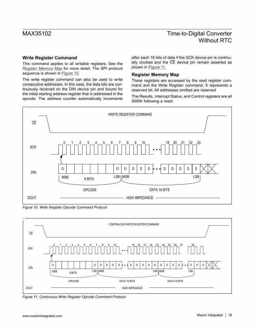
Write Register CommandThis command applies to all writable registers. See the Register Memory Map for more detail. The SPI protocol sequence is shown in Figure 10.The write register command can also be used to write consecutive addresses. In this case, the data bits are con-tinuously received on the DIN device pin and bound for the initial starting address register that is addressed in the opcode. The address counter automatically increments
after each 16 bits of data if the SCK device pin is continu-ally clocked and the CE device pin remain asserted as shown in Figure 11.
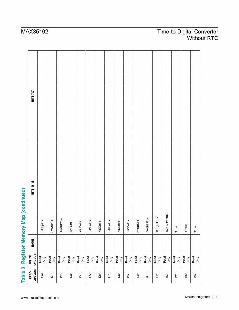
Register Memory MapThese registers are accessed by the read register com-mand and the Write Register command: X represents a reserved bit. All addresses omitted are reservedThe Results, Interrupt Status, and Control registers are all 0000h following a reset.
Figure 10. Write Register Opcode Command Protocol
Figure 11. Continuous Write Register Opcode Command Protocol
CE
SCK
DIN
DOUT
O O
OPCODE
D D D
MSB LSB8 BITS
D D D D D D
LSBMSB
HIGH IMPEDANCE
WRITE REGISTER COMMAND
DATA 16 BITS
0 1 2 3 4 5 109876 20 23222119
Figure 10
CE
SCK
DIN
DOUT
O O
OPCODE
D D D
MSB LSB8 BITS
D D D D D D
LSBMSB
HIGH IMPEDANCE
CONTINUOUS WRITE REGISTER COMMAND
DATA 16 BITS
0 1 2 3 4 5 109876 20 23222119 25 39272624
D D D D D D D
LSBMSB
DATA 16 BITS
Figure 11
MAX35102 Time-to-Digital Converter Without RTC
www.maximintegrated.com Maxim Integrated 18

Tabl
e 3.
Reg
iste
r Mem
ory
Map
REA
D
OPC
OD
EW
RIT
E O
PCO
DE
NA
ME
BIT
S[15
:8]
BIT
S[7:
0]
CO
NFI
GU
RAT
ION
REG
ISTE
RS
B6h
36h
Res
erve
d
B7h
37h
Res
erve
d
B8h
38h
TOF1
PL7
PL6
PL5
PL4
PL3
PL2
PL1
PL0
DP
L3D
PL2
DP
L1D
PL0
STO
P _P
OL
XC
T1C
T0
B9h
39h
TOF2
STO
P 2
STO
P 1
STO
P 0
T2W
V
5T2
WV
4
T2W
V
3T2
WV
2
T2W
V
1T2
WV
0TO
F_
CY
C2
TOF_
CY
C1
TOF_
C
YC
0E
N_U
P
_DN
TIM
O
UT2
TIM
O
UT1
TIM
O
UT0
BD
h3D
hTO
F6C
_OF
FSE
T R
UP
7
C_O
F FS
ET
RU
P6
C_O
F FS
ET
RU
P5
C_O
F FS
ET
RU
P4
C_O
F FS
ET
RU
P3
C_O
F FS
ET
RU
P2
C_O
F FS
ET
RU
P1
C_O
F FS
ET
RU
P0
C_O
F FS
ET
UP
7
C_O
F FS
ET
UP
6
C_O
F FS
ET
UP
5
C_O
F FS
ET
UP
4
C_O
F FS
ET
UP
3
C_O
F FS
ET
UP
2
C_O
F FS
ET
UP
1
C_O
F FS
ET
UP
0
BE
h3E
hTO
F7C
_OF
FSE
T R
DN
7
C_O
F FS
ET
RD
N6
C_O
F FS
ET
RD
N5
C_O
F FS
ET
RD
N4
C_O
F FS
ET
RD
N3
C_O
F FS
ET
RD
N2
C_O
F FS
ET
RD
N1
C_O
F FS
ET
RD
N0
C_O
F FS
ET
DN
7
C_O
F FS
ET
DN
6
C_O
F FS
ET
DN
5
C_O
F FS
ET
DN
4
C_O
F FS
ET
DN
3
C_O
F FS
ET
DN
2
C_O
F FS
ET
DN
1
C_O
F FS
ET
DN
0
C0h
40h
Tem
pera
ture
XX
XX
XX
XX
XTP
1TP
0P
RE
C
YC
2P
RE
C
YC
1P
RE
C
YC
0P
OR
T C
YC
1P
OR
T C
YC
0
C1h
41h
TOF
M
easu
re-
men
t Del
ayD
LY15
DLY
14LY
13D
LY12
DLY
11D
LY10
DLY
9D
LY8
DLY
7D
LY6
DLY
5D
LY4
DLY
3D
LY2
DLY
1D
LY0
C2h
42h
Cal
ibra
tion
and
Con
trol
XX
XX
CM
P_
EN
CM
P_
SE
LIN
T_
EN
ET_
C
ON
TC
ON
T _I
NT
CLK
_ S
2C
LK_
S1
CLK
_ S
0C
al_P
er
iod3
Cal
_P
erio
d2C
al_P
er
iod1
Cal
_P
erio
d0
C3h
43h
Osc
illat
orX
XX
XX
XX
XX
32K
_ B
P32
K_
EN
XX
XX
X
CO
NVE
RSI
ON
RES
ULT
S R
EGIS
TER
S
C4h
Rea
d O
nly
WV
RU
P
C5h
Rea
d O
nly
Hit1
UpI
nt
C6h
Rea
d O
nly
Hit1
UpF
rac
C7h
Rea
d O
nly
Hit2
UpI
nt
C8h
Rea
d O
nly
Hit2
UpF
rac
C9h
Rea
d O
nly
Hit3
UpI
nt
MAX35102 Time-to-Digital Converter Without RTC
www.maximintegrated.com Maxim Integrated 19
Tabl
e 3.
Reg
iste
r Mem
ory
Map
(con
tinue
d)R
EAD
O
PCO
DE
WR
ITE
OPC
OD
EN
AM
EB
ITS[
15:8
]B
ITS[
7:0]
CA
hR
ead
Onl
yH
it3U
pFra
c
D1h
Rea
d O
nly
AVG
UP
Int
D2h
Rea
d O
nly
AVG
UP
Frac
D3h
Rea
d O
nly
WV
RD
N
D4h
Rea
d O
nly
Hit1
DnI
nt
D5h
Rea
d O
nly
Hit1
DnF
rac
D6h
Rea
d O
nly
Hit2
DnI
nt
D7h
Rea
d O
nly
Hit2
DnF
rac
D8h
Rea
d O
nly
Hit3
DnI
nt
D9h
Rea
d O
nly
Hit3
DnF
rac
E0h
Rea
d O
nly
AVG
DN
Int
E1h
Rea
d O
nly
AVG
DN
Frac
E2h
Rea
d O
nly
TOF_
DIF
FInt
E3h
Rea
d O
nly
TOF_
DIF
FFra
c
E7h
Rea
d O
nly
T1In
t
E8h
Rea
d O
nly
T1Fr
ac
E9h
Rea
d O
nly
T2In
t
MAX35102 Time-to-Digital Converter Without RTC
www.maximintegrated.com Maxim Integrated 20

Tabl
e 3.
Reg
iste
r Mem
ory
Map
(con
tinue
d)
EA
hR
ead
Onl
yT2
Frac
REA
D
OPC
OD
EW
RIT
E O
PCO
DE
NA
ME
BIT
S[15
:8]
BIT
S[7:
0]
EB
hR
ead
Onl
yT3
Int
EC
hR
ead
Onl
yT3
Frac
ED
hR
ead
Onl
yT4
Int
EE
hR
ead
Onl
yT4
Frac
F8h
Rea
d O
nly
Cal
ibra
tionI
nt
F9h
Rea
d O
nly
Cal
ibra
tionF
rac
FAh
Rea
d O
nly
Res
erve
d
FBh
Rea
d O
nly
Res
erve
d
FCh
Rea
d O
nly
Res
erve
d
FDh
Rea
d O
nly
Res
erve
d
STAT
US
REG
ISTE
RS
FEh
Rea
d O
nly
Inte
rrup
t S
tatu
sTO
XX
TOF
TELD
OX
XX
CA
LX
XIN
ITP
OR
XX
MAX35102 Time-to-Digital Converter Without RTC
www.maximintegrated.com Maxim Integrated 21

Table 4. TOF1 RegisterConfiguration Register Descriptions
WRITE OPCODE38h
READ OPCODEB8h
POWER-ON RESET VALUE0010h
Bit 15 14 13 12 11 10 9 8
Name PL7 PL6 PL5 PL4 PL3 PL2 PL1 PL0
Bit 7 6 5 4 3 2 1 0
Name DPL3 DPL2 DPL1 DPL0 STOP_POL X CT1 CT0
BIT NAME DESCRIPTION
15:8 PL[7:0]
Pulse Launcher Size: This is a hex value that defines the number of pulses that will be launched from the pulse launcher during transmission. The range of this hex value is 00h to FFh. When PL[7:0] is set to 00h, the Pulse Launcher is disabled. Up to 127 pulses can be launched. When PL7 is set, the pulse count is clamped at 127.
7:4 DPL[3:0]
Pulse Launch Divider: This is a hex value that defines the divider ratio of the internal clock signal used to drive the Pulse Launch signal. The 4MHz external reference oscillator is used as the source for the internal clock reference. The internal reference clock is first divided by 2 to produce a 2MHz clock. The range of this hex value is 1h to Fh, resulting in a range of division from ÷2 to ÷16 of the 2MHz clock. A value of 0h is not supported and should not be programmedPulse Launch Frequency = 2MHz/(1+DPL[3:0])
DPL[3:0] PULSE LAUNCH FREQUENCY
0000b RESERVED
0001b 1MHz
0002b 666kHz
…. ….
1110b 133.33kHz
1111b 125kHz
3 STOP_POL
Stop Polarity: This bit defines the edge sensitivity of the STOP_UP and STOP_DN channel. The signal received on the STOP_UP and STOP_DN device pins will generate a stop condition for the internal TDC time count on the rising slope of this signal if this bit is set to 0. The signal received on the STOP_UP and STOP_DN device pins will generate a stop condition for the internal TDC time count on the falling slope of this signal if this bit is set to 1.
2 X Reserved
MAX35102 Time-to-Digital Converter Without RTC
www.maximintegrated.com Maxim Integrated 22

Table 4. TOF1 Register (continued)
Table 5. TOF2 Register
BIT NAME DESCRIPTION
1:0 CT[1:0]
Bias Charge Time: This is the time allotted for charging the external bias network on the STOP pins to produce common mode biasing for the analog receiver/comparator. It is based upon the 32.768 KHz crystal:
CT1 CT2
DESCRIPTION
32kHz CLOCK CYCLES (decimal) TYPICAL TIME (µs)
0 0 2 61
0 1 4 122
1 0 8 244
1 1 16 488
WRITE OPCODE39h
READ OPCODEB9h
POWER-ON RESET VALUE0000h
Bit 15 14 13 12 11 10 9 8
Name X STOP1 STOP0 T2WV5 T2WV4 T2WV3 T2WV2 T2WV1
Bit 7 6 5 4 3 2 1 0
Name T2WV0 TOF_CYC2 TOF_CYC1 TOF_CYC0 X TIMOUT2 TIMOUT1 TIMOUT0
BIT NAME DESCRIPTION
15 X Reserved
14:13 STOP[1:0]
Stop Hits: These bits set the number of stop hits to be expected and measured.
STOP1 STOP0 DESCRIPTION
0 0 1 Hit
0 1 2 Hits
1 0 3 Hits
1 1 3 Hits
12:7 T2WV[5:0]
Wave Selector for t2: These bits determine the wave number for which t2 is measured. To ensure measurement accuracy, the first wave measurable after the early edge detect is wave 2. Waves are numbered as depicted in Figure 5.
T2WV[5:0] (decimal) DESCRIPTION
0 through 2 Wave 2
3 Wave 3
4 Wave 4
MAX35102 Time-to-Digital Converter Without RTC
www.maximintegrated.com Maxim Integrated 23

Table 5. TOF2 Register (continued)BIT NAME DESCRIPTION
6:4 TOF_CYC[2:0]
TOF Duty Cycle: These bits determine the time delay between successive executions of TOF measurements. It is the start-to-start time of automatic execution of the TOF_UP and the TOF_DN and is applicable only for the TOF_DIFF command. It is based upon the 32.768kHz crystal. If the actual TOF of the acoustic path exceeds the programmed start-to-start time in this setting, then the TOF duty cycle performs as if the bit setting is 000b.
TOF_CYC[2:0]
DESCRIPTION
32kHz CLOCK CYCLES (decimal)
TYPICAL TIME 4MHz ON BETWEEN TOF_UP and TOF_DOWN
000b 0 0µs Yes
001b 4 122µs Yes
010b 8 244µs Yes
011b 16 488µs Yes
100b 24 732µs Yes
101b 32 976µs Yes
110b 546 16.65ms No
111b 655 19.97ms No
3 X Reserved
2:0 TIMOUT[2:0]
Timeout: These bits force a timeout in the time-to-digital measurement block. If the hit required to measure t1, t2, or Hit1 through Hit3 of the received signal does not occur in this time, the TO bit in the Interrupt Status register is set and the INT pin is asserted (if enabled). Additionally, any of the Conversion Results registers read FFFFh if the data for that register is invalid.
TIMOUT2 TIMOUT1 TIMOUT0 DESCRIPTION (µs)
0 0 0 128
0 0 1 256
0 1 0 512
0 1 1 1024
1 0 0 2048
1 0 1 4096
1 1 0 8192
1 1 1 16384
MAX35102 Time-to-Digital Converter Without RTC
www.maximintegrated.com Maxim Integrated 24

Table 6. TOF6 RegisterWRITE OPCODE
3DhREAD OPCODE
BDhPOWER-ON RESET VALUE
0000h
Bit 15 14 13 12 11 10 9 8
Name X X X X X X X X
Bit 7 6 5 4 3 2 1 0
Name X X X C_OFFSET UP4
C_OFFSET UP3
C_OFFSET UP2
C_OFFSET UP1
C_OFFSET UP0
BIT NAME DESCRIPTION
15:5 X Reserved
4:0 C_OFFSETUP [4:0]
Comparator Offset Upstream: These bits define an initial selected receive comparator offset voltage for the analog receiver comparator front-end. This comparator offset is used to detect the early edge wave, t1. The actual common-mode voltage is dependent upon and scales with the voltage present at the VCC pins.When the STOP_POL bit in the TOF1 register is set to zero indicating a rising edge detection of the zero crossing of the received acoustic wave, then the comparator offset is a positive value. When the STOP_POL bit in the TOF1 register is set to one indicating a falling edge detection of the zero crossing of the received acoustic wave, then the comparator offset is a negative value.The following formulas define the comparator offset voltage setting
OFFSETUPCC
OFFSETUPCC
CC
CSTOP_POL 0 Comparator Offset Voltage V3072
CSTOP_POL
(1152 + )
(111 Comparato 51- )r Offset Voltage V3072
Vwhere 1 LSB 3072
= = ×
= = ×
=
C_OFFSETUP[4:0] OFFSET (LSBs)
00h through 1Fh 0 through 31
MAX35102 Time-to-Digital Converter Without RTC
www.maximintegrated.com Maxim Integrated 25
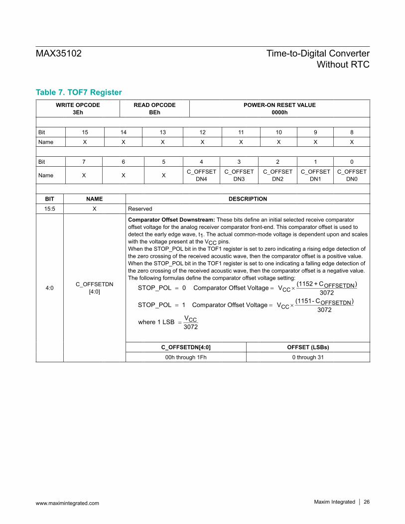
Table 7. TOF7 RegisterWRITE OPCODE
3EhREAD OPCODE
BEhPOWER-ON RESET VALUE
0000h
Bit 15 14 13 12 11 10 9 8
Name X X X X X X X X
Bit 7 6 5 4 3 2 1 0
Name X X X C_OFFSET DN4
C_OFFSET DN3
C_OFFSET DN2
C_OFFSET DN1
C_OFFSET DN0
BIT NAME DESCRIPTION
15:5 X Reserved
4:0 C_OFFSETDN [4:0]
Comparator Offset Downstream: These bits define an initial selected receive comparator offset voltage for the analog receiver comparator front-end. This comparator offset is used to detect the early edge wave, t1. The actual common-mode voltage is dependent upon and scales with the voltage present at the VCC pins. When the STOP_POL bit in the TOF1 register is set to zero indicating a rising edge detection of the zero crossing of the received acoustic wave, then the comparator offset is a positive value. When the STOP_POL bit in the TOF1 register is set to one indicating a falling edge detection of the zero crossing of the received acoustic wave, then the comparator offset is a negative value. The following formulas define the comparator offset voltage setting:
OFFSETDNCC
OFFSETDNCC
CC
CSTOP_POL 0 Comparator Offset Voltage V3072
CSTOP_POL
(1152 + )
(111 Comparato 51- )r Offset Voltage V3072
Vwhere 1 LSB 3072
= = ×
= = ×
=
C_OFFSETDN[4:0] OFFSET (LSBs)
00h through 1Fh 0 through 31
MAX35102 Time-to-Digital Converter Without RTC
www.maximintegrated.com Maxim Integrated 26
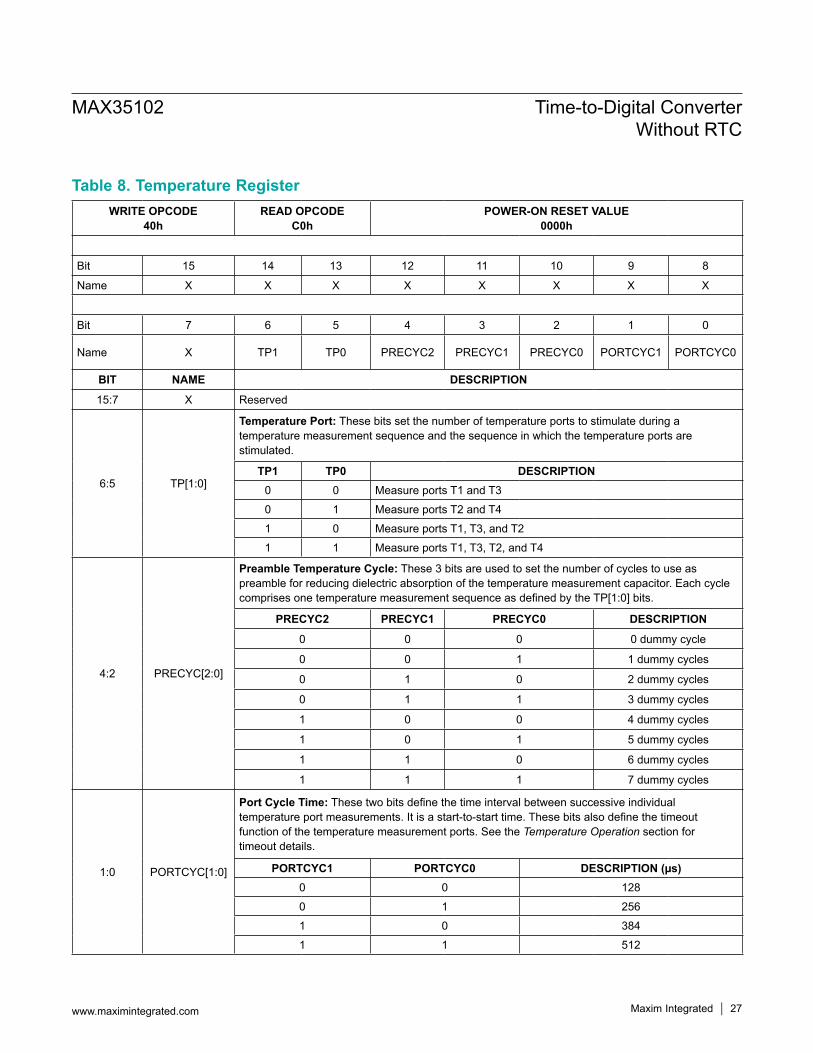
Table 8. Temperature RegisterWRITE OPCODE
40hREAD OPCODE
C0hPOWER-ON RESET VALUE
0000h
Bit 15 14 13 12 11 10 9 8
Name X X X X X X X X
Bit 7 6 5 4 3 2 1 0
Name X TP1 TP0 PRECYC2 PRECYC1 PRECYC0 PORTCYC1 PORTCYC0
BIT NAME DESCRIPTION
15:7 X Reserved
6:5 TP[1:0]
Temperature Port: These bits set the number of temperature ports to stimulate during a temperature measurement sequence and the sequence in which the temperature ports are stimulated.
TP1 TP0 DESCRIPTION0 0 Measure ports T1 and T3
0 1 Measure ports T2 and T4
1 0 Measure ports T1, T3, and T2
1 1 Measure ports T1, T3, T2, and T4
4:2 PRECYC[2:0]
Preamble Temperature Cycle: These 3 bits are used to set the number of cycles to use as preamble for reducing dielectric absorption of the temperature measurement capacitor. Each cycle comprises one temperature measurement sequence as defined by the TP[1:0] bits.
PRECYC2 PRECYC1 PRECYC0 DESCRIPTION
0 0 0 0 dummy cycle
0 0 1 1 dummy cycles
0 1 0 2 dummy cycles
0 1 1 3 dummy cycles
1 0 0 4 dummy cycles
1 0 1 5 dummy cycles
1 1 0 6 dummy cycles
1 1 1 7 dummy cycles
1:0 PORTCYC[1:0]
Port Cycle Time: These two bits define the time interval between successive individual temperature port measurements. It is a start-to-start time. These bits also define the timeout function of the temperature measurement ports. See the Temperature Operation section for timeout details.
PORTCYC1 PORTCYC0 DESCRIPTION (µs)0 0 128
0 1 256
1 0 384
1 1 512
MAX35102 Time-to-Digital Converter Without RTC
www.maximintegrated.com Maxim Integrated 27

Table 9. ToF Measurement Delay Register
Table 10. Calibration and Control Register
WRITE OPCODE41h
READ OPCODEC1h
POWER-ON RESET VALUE0000h
Bit 15 14 13 12 11 10 9 8
Name DLY15 DLY14 DLY13 DLY12 DLY11 DLY10 DLY9 DLY8
Bit 7 6 5 4 3 2 1 0
Name DLY7 DLY6 DLY5 DLY4 DLY3 DLY2 DLY1 DLY0
BIT NAME DESCRIPTION
15:0 DLY[15:0]
This is hexadecimal value ranging from 0000h to FFFFh (decimal 0 to 65535). It is a multiple of the 4MHz crystal period (250ns). Settings less than 0012h are reserved and should not be used. The analog comparator driven by the STOP_UP and STOP_DN device pins does not generate a stop condition until this delay, counted from the internally generated start pulse for the acoustic wave, has expired. This delay applies to early edge detect wave. Care must be taken to set the TIMOUT bits in the TOF2 register so that a timeout interrupt does not occur before this delay expires.
WRITE OPCODE42h
READ OPCODEC2h
POWER-ON RESET VALUE0000h
Bit 15 14 13 12 11 10 9 8
Name X X X X CMP_EN CMP_SEL INT_EN X
Bit 7 6 5 4 3 2 1 0
Name X CLK_S2 CLK_S1 CLK_S0 CAL_ PERIOD3
CAL_ PERIOD2
CAL_ PERIOD1
CAL_ PERIOD0
BIT NAME DESCRIPTION15:12 X Reserved
11 CMP_ENComparator/UP_DN Output Enable:1 = CMP_OUT/UP_DN output device pin is enabled.0 = CMP_OUT/UP_DN output device pin is driven low.
MAX35102 Time-to-Digital Converter Without RTC
www.maximintegrated.com Maxim Integrated 28

Table 10. Calibration and Control Register (continued)BIT NAME DESCRIPTION
10 CMP_SEL
Comparator/UP_DN Output Select: This bit selects the output function of the CMP_OUT/UP_DN pin and is only used when CMP_EN = 1.1 = CMP_EN: The output monitors the receiver front end comparator output.0 = UP_DN: The output monitors the launch direction of the pulse launcher. High Output: Upstream measurement (Launch_UP to STOP_UP) Low Output: Downstream measurement (Launch_DN to STOP_DN)
9 INT_EN Interrupt Enable: This bit, when set, enables the INT pin. All interrupt sources are wire-ORed to the INT pin.
8 X Reserved
7 X Reserved
6:4 CLK_S[2:0]
Clock Settling Time: These bits define the time interval that the MAX35102 waits after enabling the 4MHz clock for it to stabilize before making any measurements of time or temperature.
CLK_S2 CLK_S1 CLK_S0DESCRIPTION
32kHz CLOCK CYCLES TYPICAL TIME
0 0 0 16 488µs
0 0 1 48 1.46ms
0 1 0 96 2.93ms
0 1 1 128 3.9ms
1 0 0 168 5.13ms
1 0 1 4MHz oscillator on continuously
1 1 0 4MHz oscillator on continuously
1 1 1 4MHz oscillator on continuously
3:0 CAL_PERIOD[3:0]
4MHz Ceramic Oscillator Calibration Period: These bits define the number of 32.768kHz oscillator periods to measure for determination of the 4MHz ceramic oscillator period.32kHz clock cycles = 1+ CAL_PERIOD[3:0]
CAL_PERIOD[3:0] (decimal)DESCRIPTION
32kHz CLOCK CYCLES (decimal)
32kHz CLOCK CYCLES (µs)
0 1 30.5
1 2 61
…. …. ….
14 15 457.7
15 16 488.0
MAX35102 Time-to-Digital Converter Without RTC
www.maximintegrated.com Maxim Integrated 29

Table 11. Oscillator Register
Table 12. Interrupt Status Register
Status Register Descriptions
WRITE OPCODE43h
READ OPCODEC3h
POWER-ON RESET VALUE0000h
Bit 15 14 13 12 11 10 9 8
Name X X X X X X X X
Bit 7 6 5 4 3 2 1 0
Name X 32K_BP 32K_EN EOSC X X X X
BIT NAME DESCRIPTION15:7 X Reserved
6 32K_BP32kHz Bypass: This bit, when set, allows an external CMOS-level 32.768kHz signal to be applied to the 32KX1 device pin. The internal 32.768kHz oscillator is bypassed and the external signal is driven into the MAX35102 core.
5 32K_EN 32kHz Clock Output Enable: This bit enables the 32KOUT device pin to drive a CMOS-level square wave representation of the 32kHz crystal.
4 EOSC Enable Oscillator: This active-low bit when set to logic 0 starts the 32kHz oscillator. When this bit is set to logic 1, the oscillator is stopped.
3:0 X Reserved
WRITE OPCODERead Only
READ OPCODEFEh
POWER-ON RESET VALUE0000h
Bit 15 14 13 12 11 10 9 8
Name TO X X TOF TE X X X
Bit 7 6 5 4 3 2 1 0
Name X CAL X X INIT POR X X
Note: This register is read only and bits are self-clearing upon a read to this register. See the Device Interrupt Operations section for more information.
BIT NAME DESCRIPTION
15 TO Timeout: The TO bit is set if any one of the t1, t2, Hit1 through Hit3, or temperature measure-ments do not occur within the associated timeout window.
14:13 X Reserved
MAX35102 Time-to-Digital Converter Without RTC
www.maximintegrated.com Maxim Integrated 30

Conversion Results Register DescriptionsThe devices conversion results registers are all read-only volatile SRAM. The POR value for all registers is 0000h.
Table 12. Interrupt Status Register (continued)
Table 13. Conversion Results Registers Description
BIT NAME DESCRIPTION12 TOF Time of Flight: Set when the TOF_UP, TOF_DN, or TOF_DIFF command has completed.
11 TE Temperature: Set when the temperature command has completed.
10:7 X Reserved
6 CAL Calibrate: Set after completion of the Calibrate command when the command is manually sent by the host microprocessor.
5 X Reserved
4 X Reserved
3 INIT Initialize: Set when the Initialize command has completed.
2 POR Power-On-Reset: Set when the MAX35102 has been successfully powered by application of VCC. Upon application of power, the SPI port becomes inactive until this bit has been set.
1:0 X Reserved
READ ONLY ADDRESS NAME DESCRIPTION
C4h WVRUP
Bit 15 through Bit 8 holds the 8-bit value of the pulse width ratio (t1 ÷ t2).for the upstream measurement. Each bit is weighted as follows:
BIT 15 BIT 14 BIT 13 BIT 12 BIT 11 BIT 10 BIT 9 BIT 81 0.5 0.25 0.125 0.0625 0.03125 0.015625 0.0078125
Bit 7 thru bit 0 holds the 8-bit value of the pulse width ratio (t2 ÷ tideal) where tideal is equal to half the period of the Pulse Launch Frequency for the upstream measurement. Each bit is weighted as follows:
BIT 7 BIT 6 BIT 5 BIT 4 BIT 3 BIT 2 BIT 1 BIT 0
1 0.5 0.25 0.125 0.0625 0.03125 0.015625 0.0078125
The maximum value of each of these ratios is 1.9921875.
C5h Hit1UPInt15-bit fixed-point integer value of the first hit in the upstream direction. This integer portion is a binary representation of the number of t4MHz periods that contribute to the time results. The maximum size of the integer is 7FFFh or (215 - 1) x t4MHz.
C6h Hit1UPFrac16-bit fractional value of the first hit in the upstream direction. This fractional portion is a binary representation of one t4MHz period quantized to a 16-bit resolution. The maximum size of the fraction is FFFFh or (216 - 1)/216 x t4MHz.
MAX35102 Time-to-Digital Converter Without RTC
www.maximintegrated.com Maxim Integrated 31

Table 13. Conversion Results Registers Description (continued)READ ONLY ADDRESS NAME DESCRIPTION
C7h Hit2UPInt15-bit fixed-point integer value of the second hit in the upstream direction. This integer portion is a binary representation of the number of t4MHz periods that contribute to the time results. The maximum size of the integer is 7FFFh or (215 - 1) x t4MHz.
C8h Hit2UPFrac16-bit fractional value of the second hit in the upstream direction. This fractional portion is a binary representation of one t4MHz period quantized to a 16-bit resolution. The maximum size of the fraction is FFFFh or (216 - 1)/216 x t4MHz.
C9h Hit3UPInt15-bit fixed-point integer value of the third hit in the upstream direction. This integer portion is a binary representation of the number of t4MHz periods that contribute to the time results. The maximum size of the integer is 7FFFh or (215 - 1) x t4MHz.
CAh Hit3UPFrac16-bit fractional value of the third hit in the upstream direction. This fractional portion is a binary representation of one t4MHz period quantized to a 16-bit resolution. The maximum size of the fraction is FFFFh or (216 - 1)/216 x t4MHz.
D1h AVGUPInt15-bit fixed-point integer value of the average of the hits recorded in the upstream direction This integer portion is a binary representation of the number of t4MHz periods that contribute to the time results. The maximum size of the integer is 7FFFh or (215 - 1) x t4MHz.
D2h AVGUPFrac16-bit fractional value of the average of the hits recorded in the upstream direction. This fractional portion is a binary representation of one t4MHz period quantized to a 16-bit resolution. The maximum size of the fraction is FFFFh or (216 - 1)/216 x t4MHz.
D3h WVRDN
Bit 15 through Bit 8 holds the 8 bit value of the pulse width ratio (t1/t2).for the downstream measurement. Each bit is weighted as follows:
BIT 15 BIT 14 BIT 13 BIT 12 BIT 11 BIT 10 BIT 9 BIT 8
1 0.5 0.25 0.125 0.0625 0.03125 0.015625 0.0078125
Bit 7 thru bit 0 holds the 8 bit value of the pulse width ratio (t2/tideal) where tideal is equal to half the period of the pulse launch frequency for the downstream measurement. Each bit is weighted as follows:
BIT 7 BIT 6 BIT 5 BIT 4 BIT 3 BIT 2 BIT 1 BIT 0
1 0.5 0.25 0.125 0.0625 0.03125 0.015625 0.0078125
The maximum value of each of these ratios is 1.9921875.
D4h Hit1DNInt15-bit fixed-point integer value of the first hit in the downstream direction. This integer portion is a binary representation of the number of t4MHz periods that contribute to the time results. The maximum size of the integer is 7FFFh or (215 - 1) x t4MHz.
D5h Hit1DNFrac16-bit fractional value of the first hit in the downstream direction. This fractional portion is a binary representation of one t4MHz period quantized to a 16-bit resolution. The maximum size of the fraction is FFFFh or (216 - 1)/216 x t4MHz.
D6h Hit2DNInt15-bit fixed-point integer value of the second hit in the downstream direction. This integer portion is a binary representation of the number of t4MHz periods that contribute to the time results. The maximum size of the integer is 7FFFh or (215 - 1) x t4MHz.
MAX35102 Time-to-Digital Converter Without RTC
www.maximintegrated.com Maxim Integrated 32

Table 13. Conversion Results Registers Description (continued)READ ONLY ADDRESS NAME DESCRIPTION
D7h Hit2DNFrac16-bit fractional value of the second hit in the downstream direction. This fractional portion is a binary representation of one t4MHz period quantized to a 16-bit resolution. The maximum size of the fraction is FFFFh or (216 - 1)/216 x t4MHz.
D8h Hit3DNInt15-bit fixed-point integer value of the third hit in the downstream direction. This integer portion is a binary representation of the number of t4MHz periods that contribute to the time results. The maximum size of the integer is 7FFFh or (215 - 1) x t4MHz.
D9h Hit3DNFrac16-bit fractional value of the third hit in the downstream direction. This fractional portion is a binary representation of one t4MHz period quantized to a 16-bit resolution. The maximum size of the fraction is FFFFh or (216 - 1)/216 x t4MHz.
E0h AVGDNInt15-bit fixed-point integer value of the average of the hit times recorded in the downstream direction. This integer portion is a binary representation of the number of t4MHz periods that contribute to the time results. The maximum size of the integer is 7FFFh or (215 – 1) x t4MHz.
E1h AVGDNFrac16-bit fractional value of the average of the hit times recorded in the downstream direction. This fractional portion is a binary representation of one period quantized to a 16-bit resolution. The maximum size of the fraction is FFFFh or (216 – 1)/216 x t4MHz.
E2h TOF_DIFFInt
16-bit fixed-point two’s-complement integer portion of the difference of the averages for the hits recorded in both the upstream and downstream directions. It is computed as:
AVGUP – AVGDNThis integer represents the number of t4MHz periods that contribute to computation. The maximum size of the integer is 7FFFh or (215 – 1) x t4MHz. The minimum size of this integer is 8000h or -215 x t4MHz.
E3h TOF_ DIFFFrac
16-bit fractional portion of the two’s complement difference of the averages for the hits recorded in both the upstream and downstream directions. This fractional portion is a binary representation of one t4MHz period quantized to a 16-bit resolution. The maximum size of the fraction is FFFFh or (216 - 1)/216 x t4MHz.
E7h T1Int
15-bit fixed-point integer value of the time taken to discharge the timing capacitor through the RTD connected to the T1 device pin. This integer portion is a binary representation of the number of t4MHz periods that contribute to the time results. The maximum size of the integer is 7FFFh or (215 - 1) x t4MHz.
E8h T1Frac
16-bit fractional value of the time taken to charge the timing capacitor through the RTD connected to the T1 device pin. This fractional portion is a binary representation of one t4MHz period quantized to a 16-bit resolution. The maximum size of the fraction is FFFFh or (216 - 1)/216 x t4MHz.
E9h T2Int
15-bit fixed-point integer value of the time taken to charge the timing capacitor through the RTD connected to the T2 device pin. This integer portion is a binary representation of the number of periods that contribute to the time results. The maximum size of the integer is 7FFFh or (215 - 1) x t4MHz.
EAh T2Frac
16-bit fractional value of the time taken to charge the timing capacitor through the RTD connected to the T2 device pin. This fractional portion is a binary representation of one t4MHz period quantized to a 16-bit resolution. The maximum size of the fraction is FFFFh or (216 - 1)/216 x t4MHz.
MAX35102 Time-to-Digital Converter Without RTC
www.maximintegrated.com Maxim Integrated 33

Table 19. Conversion Results Registers Description (continued)READ ONLY ADDRESS NAME DESCRIPTION
EBh T3Int
15-bit fixed-point integer value of the time taken to charge the timing capacitor through the RTD connected to the T3 device pin. This integer portion is a binary representation of the number of t4MHz periods that contribute to the time results. The maximum size of the integer is 7FFFh or (215 - 1) x t4MHz.
ECh T3Frac
16-bit fractional value of the time taken to charge the timing capacitor through the RTD connected to the T3 device pin. This fractional portion is a binary representation of one t4MHz period quantized to a 16-bit resolution. The maximum size of the fraction is FFFFh or (216 - 1)/216 x t4MHz.
EDh T4Int
15-bit fixed-point integer value of the time taken to charge the timing capacitor through the RTD connected to the T4 device pin. This integer portion is a binary representation of the number of t4MHz periods that contribute to the time results. The maximum size of the integer is 7FFFh or (215 - 1) x t4MHz.
EEh T4Frac
16-bit fractional value of the time taken to charge the timing capacitor through the RTD connected to the T4 device pin. This fractional portion is a binary representation of one t4MHz period quantized to a 16-bit resolution. The maximum size of the fraction is FFFFh or (216 - 1)/216 x t4MHz.
F8h Calibration Int
15-bit fixed-point integer value of the time taken to measure the period of the 32.768kHz crystal oscillator during execution of the calibrate command. This integer portion is a binary representation of the number of t4MHz periods that contribute to the time results. The maximum size of the integer is 7FFFh or (215 - 1) x t4MHz.
F9h Calibration Frac
16-bit fractional value of the time taken to measure the period of the 32.768kHz crystal oscillator during execution of the calibrate command. This fractional portion is a binary representation of one t4MHz period quantized to a 16-bit resolution. The maximum size of the fraction is FFFFh or (216 - 1)/216 x t4MHz.
FAh Reserved
FBh Reserved
FCh Reserved
FDh Reserved
MAX35102 Time-to-Digital Converter Without RTC
www.maximintegrated.com Maxim Integrated 34

4-WIREINTERFACE
ANALOG SWITCHING AND BIAS CONTROL
TIME-TO-DIGITAL CONVERTER
PROGRAMMABLE ALU
DATA AND STATUS
REGISTERS
STATE MACHINE CONTROLLER
CONFIGURATION REGISTERS
INTERNAL LDO
PULSE LAUNCHER
X1
12pF
X2
32.768kHz
32KX1
12pF
32KX0
12pF
4MHz
12pF
32KOUT
MICROCONTROLLER
T1 T2 T3 T4 TC
PT 1
000
1k (50ppm) METAL FILM
100 nF COG (NP0) (30ppm/C)
DIN
CE
DOUT
SCK
RST
INT
STOP_UP
LAUNCH_UP
LAUNCH_DN
STOP_DN
VCC
BYPASS100nFLOW ESR
PIEZOELECTRIC TRANSDUCERS
CMP_OUT/UP_DN
VCCVCC
3.6V
HIGH-SPEED AND 32kHz OSCILLATORS TEMPERATURE MEASUREMENT
MAX35102
GNDGNDGNDGNDGND
PT 1
000
3.6V
GND
Typical Application Circuit
MAX35102 Time-to-Digital Converter Without RTC
www.maximintegrated.com Maxim Integrated 35
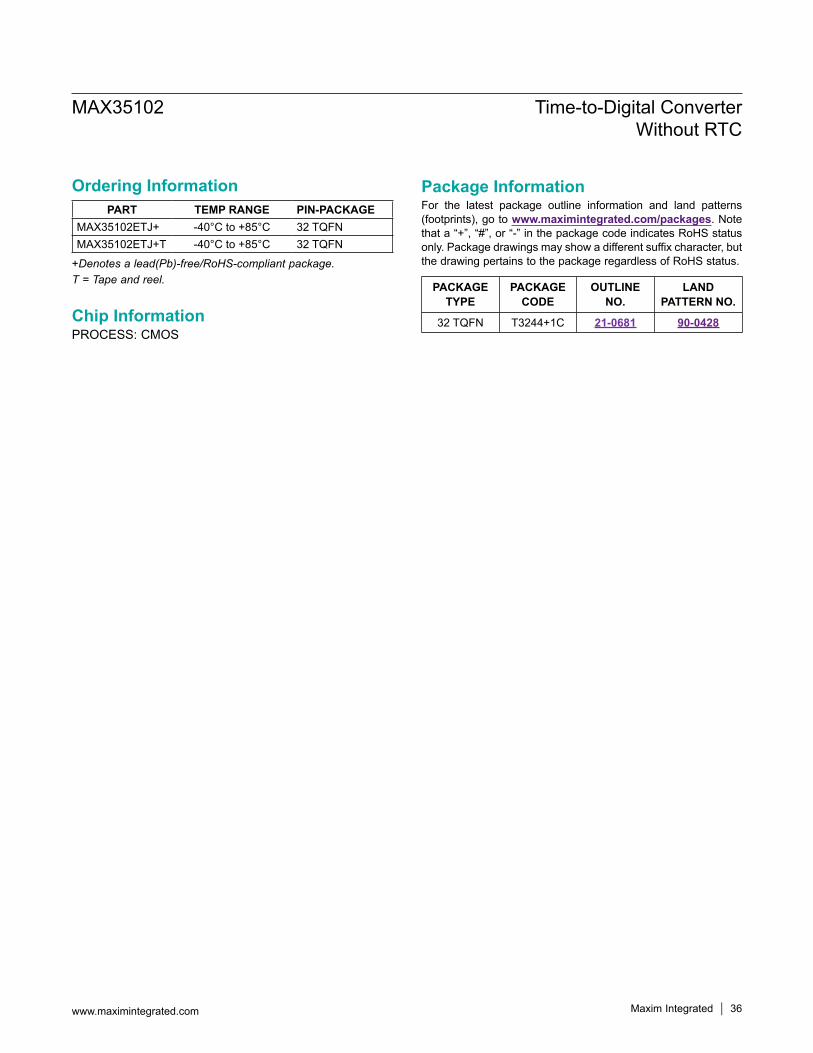
+Denotes a lead(Pb)-free/RoHS-compliant package. T = Tape and reel.
PART TEMP RANGE PIN-PACKAGEMAX35102ETJ+ -40°C to +85°C 32 TQFNMAX35102ETJ+T -40°C to +85°C 32 TQFN
PACKAGE TYPE
PACKAGE CODE
OUTLINE NO.
LAND PATTERN NO.
32 TQFN T3244+1C 21-0681 90-0428
MAX35102 Time-to-Digital Converter Without RTC
www.maximintegrated.com Maxim Integrated 36
Package InformationFor the latest package outline information and land patterns (footprints), go to www.maximintegrated.com/packages. Note that a “+”, “#”, or “-” in the package code indicates RoHS status only. Package drawings may show a different suffix character, but the drawing pertains to the package regardless of RoHS status.
Chip InformationPROCESS: CMOS
Ordering Information

REVISION NUMBER
REVISION DATE DESCRIPTION PAGES
CHANGED0 11/14 Initial release —
Maxim Integrated cannot assume responsibility for use of any circuitry other than circuitry entirely embodied in a Maxim Integrated product. No circuit patent licenses are implied. Maxim Integrated reserves the right to change the circuitry and specifications without notice at any time. The parametric values (min and max limits) shown in the Electrical Characteristics table are guaranteed. Other parametric values quoted in this data sheet are provided for guidance.
Maxim Integrated and the Maxim Integrated logo are trademarks of Maxim Integrated Products, Inc.
MAX35102 Time-to-Digital Converter Without RTC
© 2014 Maxim Integrated Products, Inc. 37
Revision History
For pricing, delivery, and ordering information, please contact Maxim Direct at 1-888-629-4642, or visit Maxim Integrated’s website at www.maximintegrated.com.