features and operation modes of flextimer module on s32k · eight channels which work either...
TRANSCRIPT

© 2016 NXP B.V.
Preliminary Information, Subject to Change without Notice
Features and Operation Modes of FlexTimer
Module on S32K
1. Introduction
This application note describes the multiple features
and operation modes of the FlexTimer (FTM) module
supported by code examples and oscilloscope
snapshots. The FTM module is used on many Kinetis
and Vybrid MCUs. However, this application note is
primarily focused on the S32K product series of 32-bit
automotive MCUs. The FTM module is an enhanced
version of the Timer/PWM module (TPM) that
provides new features for motor-control, lighting, and
power-conversion applications. The key enhancements
are:
• Signed-up counter
• Hardware dead-time insertion
• Fault-control inputs
• Enhanced triggering functionality
• Initialization and polarity control
The masking, inverting, polarity and fault control, and
hardware dead-time insertion are the main features of
the FTM module dedicated for motor-control
applications. They provide greater flexibility and they
significantly reduce the CPU load. On the other hand,
the FTM module retains standard timer functions (such
as the input capture or output compare modes) if it is
not used for motor control. This makes FTM more
flexible, covering a wide range of applications.
NXP Semiconductors Document Number: AN5303
Application Note Rev. 0 , 06/2016
Contents
1. Introduction ........................................................................ 1 2. FTM Overview ................................................................... 2 3. FTM Operation Modes ....................................................... 3
3.1. Edge-align PWM (EPWM) mode ........................... 3 3.2. Center-align PWM (CPWM) mode ......................... 4 3.3. Complementary mode and dead-time insertion ....... 6 3.4. Combine mode ........................................................ 7 3.5. Single-edge capture mode ....................................... 9 3.6. Dual-edge capture mode ........................................ 11 3.7. Quadrature decoder mode ..................................... 13
4. FTM Features ................................................................... 15 4.1. Masking, inverting, and software-controlling
features .............................................................................. 15 4.2. Fault control feature .............................................. 16 4.3. Updating FTM registers ........................................ 19 4.4. Global Time Base (GTB) ...................................... 28 4.5. ADC triggering by FTM and PDB modules .......... 30
5. Revision History ............................................................... 33

FTM Overview
Features and Operation Modes of FlexTimer Module on S32K, Application Note, Rev. 0, 06/2016
2 Preliminary Information, Subject to Change without Notice NXP Semiconductors
2. FTM Overview
The FTM module has a single 16-bit counter that is used by the FTM channels for either the input or
output modes. There are three possible clock sources that can be selected for the FTM counter: the
system clock, the fixed-frequency clock, and the external clock (see the Clock Distribution chapter in
the S32K family reference manual for a detailed clocking description). The selected counter-clock signal
then passes through a pre-scaler which enables dividing the clock source by up to 128 by setting PS[2:0]
in the FTM_SC register. If the CPWMS bit in the FTM_SC register is disabled, the FTM counter
operates in the up-counting mode. Otherwise, it operates in the up/down-counting mode.
The current implementation of the S32K device is equipped with four FTMs. Each FTM module has
eight channels which work either independently or in pairs (CH0/CH1, CH2/CH3, CH4/CH5, and
CH5/CH6). All channels can be configured for the input capture, output compare, or edge/center-align
PWM modes. In the edge-align PWM mode, the FTM channel pairs can work in the complementary
or/and combine modes. In addition, FTM1 and FTM2 are able to work in the quadrature-decoder mode
that enables processing signals from the incremental rotary position sensor (encoder). This table shows
the channels’ modes selection.
Table 1. Channels’ modes selection
DECAPEN MCOMBINE COMBINE CPWMS MSnB:
MSnA
ELSnB:
ELSnA Mode Configuration
0 0
0
0
00
01
Input capture
Capture on rising edge only
10 Capture on falling edge only
11 Capture on rising or falling edge
01
01 Output
compare
Toggle output on match
10 Clear output on match
11 Set output on match
1X
10 Edge-align
PWM
High-true pulses (clear output on
match)
X1 Low-true pulses (set output on
match)
1 XX
10 Center-align
PWM
High-true pulses (clear output on
match)
X1 Low-true pulses (set output on
match)
1 0 XX
10
Combine
PWM
High-true pulses (set on channel
(n) match, and clear on channel
(n+1) match)
X1
Low-true pulses (clear on channel
(n) match, and set on channel
(n+1) match)
1 0 0 XX
10 Modified
combine
PWM
High-true pulses (set on channel
(n) match, and clear on channel
(n+1) match)
X1
Low-true pulses (clear on channel
(n) match, and set on channel
(n+1) match)
1 0 0 0
X0 See
Table 2
Dual edge
capture
One-shot capture mode
X1 Continuous capture mode
FTM Operation Modes
Features and Operation Modes of FlexTimer Module on S32K, Application Note, Rev. 0, 06/2016
NXP Semiconductors Preliminary Information, Subject to Change without Notice 3
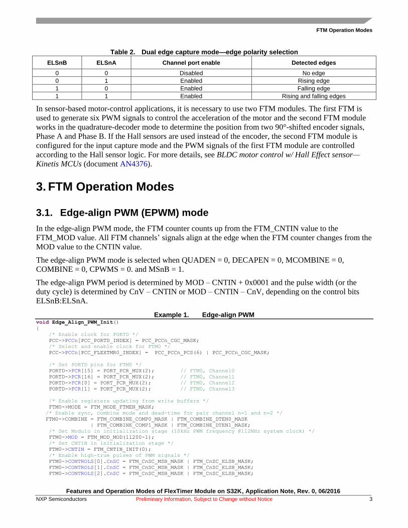
Table 2. Dual edge capture mode—edge polarity selection
ELSnB ELSnA Channel port enable Detected edges
0 0 Disabled No edge
0 1 Enabled Rising edge
1 0 Enabled Falling edge
1 1 Enabled Rising and falling edges
In sensor-based motor-control applications, it is necessary to use two FTM modules. The first FTM is
used to generate six PWM signals to control the acceleration of the motor and the second FTM module
works in the quadrature-decoder mode to determine the position from two 90°-shifted encoder signals,
Phase A and Phase B. If the Hall sensors are used instead of the encoder, the second FTM module is
configured for the input capture mode and the PWM signals of the first FTM module are controlled
according to the Hall sensor logic. For more details, see BLDC motor control w/ Hall Effect sensor—
Kinetis MCUs (document AN4376).
3. FTM Operation Modes
3.1. Edge-align PWM (EPWM) mode
In the edge-align PWM mode, the FTM counter counts up from the FTM_CNTIN value to the
FTM_MOD value. All FTM channels’ signals align at the edge when the FTM counter changes from the
MOD value to the CNTIN value.
The edge-align PWM mode is selected when QUADEN = 0, DECAPEN = 0, MCOMBINE = 0,
COMBINE = 0, CPWMS = 0. and MSnB = 1.
The edge-align PWM period is determined by MOD – CNTIN + 0x0001 and the pulse width (or the
duty cycle) is determined by CnV – CNTIN or MOD – CNTIN – CnV, depending on the control bits
ELSnB:ELSnA.
Example 1. Edge-align PWM void Edge_Align_PWM_Init()
{
/* Enable clock for PORTD */
PCC->PCCn[PCC_PORTD_INDEX] = PCC_PCCn_CGC_MASK;
/* Select and enable clock for FTM0 */
PCC->PCCn[PCC_FLEXTMR0_INDEX] = PCC_PCCn_PCS(6) | PCC_PCCn_CGC_MASK;
/* Set PORTD pins for FTM0 */
PORTD->PCR[15] = PORT_PCR_MUX(2); // FTM0, Channel0
PORTD->PCR[16] = PORT_PCR_MUX(2); // FTM0, Channel1
PORTD->PCR[0] = PORT_PCR_MUX(2); // FTM0, Channel2
PORTD->PCR[1] = PORT_PCR_MUX(2); // FTM0, Channel3
/* Enable registers updating from write buffers */
FTM0->MODE = FTM_MODE_FTMEN_MASK;
/* Enable sync, combine mode and dead-time for pair channel n=1 and n=2 */
FTM0->COMBINE = FTM_COMBINE_COMP0_MASK | FTM_COMBINE_DTEN0_MASK
| FTM_COMBINE_COMP1_MASK | FTM_COMBINE_DTEN1_MASK;
/* Set Modulo in initialization stage (10kHz PWM frequency @112MHz system clock) */
FTM0->MOD = FTM_MOD_MOD(11200-1);
/* Set CNTIN in initialization stage */
FTM0->CNTIN = FTM_CNTIN_INIT(0);
/* Enable high-true pulses of PWM signals */
FTM0->CONTROLS[0].CnSC = FTM_CnSC_MSB_MASK | FTM_CnSC_ELSB_MASK;
FTM0->CONTROLS[1].CnSC = FTM_CnSC_MSB_MASK | FTM_CnSC_ELSB_MASK;
FTM0->CONTROLS[2].CnSC = FTM_CnSC_MSB_MASK | FTM_CnSC_ELSB_MASK;

FTM Operation Modes
Features and Operation Modes of FlexTimer Module on S32K, Application Note, Rev. 0, 06/2016
4 Preliminary Information, Subject to Change without Notice NXP Semiconductors
FTM0->CONTROLS[3].CnSC = FTM_CnSC_MSB_MASK | FTM_CnSC_ELSB_MASK;
/* Set channel value in initialization stage */
FTM0->CONTROLS[0].CnV=FTM_CnV_VAL(5600); // 50% duty cycle
FTM0->CONTROLS[1].CnV=FTM_CnV_VAL(5600); // 50% duty cycle
FTM0->CONTROLS[2].CnV=FTM_CnV_VAL(2800); // 25% duty cycle
FTM0->CONTROLS[3].CnV=FTM_CnV_VAL(2800); // 25% duty cycle
/* Reset FTM counter */
FTM0->CNT = 0;
/* Insert deadtime (1us) */
FTM0->DEADTIME = FTM_DEADTIME_DTPS(3) | FTM_DEADTIME_DTVAL(7);
/* Clock selection and enabling PWM generation */
FTM0->SC = FTM_SC_CLKS(1) | FTM_SC_PWMEN0_MASK | FTM_SC_PWMEN1_MASK | FTM_SC_PWMEN2_MASK |
FTM_SC_PWMEN3_MASK;
}
Up counter period
FTM0_CH0
FTM0_CH1
FTM0_CH2
FTM1_CH3
Figure 1. Edge-align PWM
In Figure 1, the scope channels CH1, CH2, CH3, and CH4 represent FTM_CH0, FTM_CH1,
FTM_CH2, and FTM_CH3 of the FTM module, respectively. The first channel pair
(FTM_CH0/FTM_CH1) and the second channel pair (FTM_CH2/FTM_CH3) work in the
complementary mode with 50 % and 25 % duty cycles, respectively. The second channel pair
(FTM_CH2/FTM_CH3) demonstrates the edge alignment.
3.2. Center-align PWM (CPWM) mode
In the center-align PWM mode, the FTM counter counts up from FTM_CNTIN to FTM_MOD and then
counts down from FTM_MOD to FTM_CTNIN. All FTM channels’ signals align at the point where the
FTM counter reaches the FTM_MOD value. The center-align PWM mode is selected when
QUADEN = 0, DECAPEN = 0, MCOMBINE = 0, COMBINE = 0, and CPWMS = 1.

FTM Operation Modes
Features and Operation Modes of FlexTimer Module on S32K, Application Note, Rev. 0, 06/2016
NXP Semiconductors Preliminary Information, Subject to Change without Notice 5
The duty cycle of the center-align PWM is determined as 2 × (CnV − CNTIN). The period is determined
as 2 × (MOD − CNTIN).
Example 2. Center-align PWM void Center_Align_PWM_Init()
{
/* Enable clock for PORTD */
PCC->PCCn[PCC_PORTD_INDEX] = PCC_PCCn_CGC_MASK;
/* Select and enable clock for FTM0 */
PCC->PCCn[PCC_FLEXTMR0_INDEX] = PCC_PCCn_PCS(6) | PCC_PCCn_CGC_MASK;
/* Set PORTD pins for FTM0 */
PORTD->PCR[15] = PORT_PCR_MUX(2);
PORTD->PCR[16] = PORT_PCR_MUX(2);
PORTD->PCR[0] = PORT_PCR_MUX(2);
PORTD->PCR[1] = PORT_PCR_MUX(2);
/* Select up-down counter for Center-Align PWM */
FTM0->SC = FTM_SC_CPWMS_MASK;
/* Combine mode and dead-time enable for channel0 and channel1 */
FTM0->COMBINE = FTM_COMBINE_COMP0_MASK | FTM_COMBINE_DTEN0_MASK;
/* Combine mode and dead-time enable for channel2 and channel3 */
FTM0->COMBINE |= FTM_COMBINE_COMP1_MASK | FTM_COMBINE_DTEN1_MASK;
/* Set Modulo (10kHz PWM frequency @112MHz system clock) */
FTM0->MOD = FTM_MOD_MOD(5600-1);
/* Set CNTIN */
FTM0->CNTIN = FTM_CNTIN_INIT(0);
/* High-true pulses of PWM signals */
FTM0->CONTROLS[0].CnSC = FTM_CnSC_ELSB_MASK;
FTM0->CONTROLS[1].CnSC = FTM_CnSC_ELSB_MASK;
FTM0->CONTROLS[2].CnSC = FTM_CnSC_ELSB_MASK;
FTM0->CONTROLS[3].CnSC = FTM_CnSC_ELSB_MASK;
/* Set Channel Value */
FTM0->CONTROLS[0].CnV=FTM_CnV_VAL(2800); // 50% duty cycle
FTM0->CONTROLS[1].CnV=FTM_CnV_VAL(2800); // 50% duty cycle
FTM0->CONTROLS[2].CnV=FTM_CnV_VAL(1400); // 25% duty cycle
FTM0->CONTROLS[3].CnV=FTM_CnV_VAL(1400); // 25% duty cycle
/* FTM counter reset */
FTM0->CNT = 0;
/* Insert DeadTime (1us) */
FTM0->DEADTIME = FTM_DEADTIME_DTPS(3) | FTM_DEADTIME_DTVAL(7);
/* Clock selection and enabling PWM generation */
FTM0->SC |= FTM_SC_CLKS(1) | FTM_SC_PWMEN0_MASK | FTM_SC_PWMEN1_MASK | FTM_SC_PWMEN2_MASK |
FTM_SC_PWMEN3_MASK;
}

FTM Operation Modes
Features and Operation Modes of FlexTimer Module on S32K, Application Note, Rev. 0, 06/2016
6 Preliminary Information, Subject to Change without Notice NXP Semiconductors
Up-down counter period
FTM0_CH0
FTM0_CH1
FTM0_CH2
FTM1_CH3
Figure 2. Center-align PWM
In Figure 2, the scope channels CH1, CH2, CH3, and CH4 represent FTM_CH0, FTM_CH1,
FTM_CH2, and FTM_CH3 of the FTM module, respectively. The first channel pair
(FTM_CH0/FTM_CH1) and the second channel pair (FTM_CH2/FTM_CH3) work in the
complementary mode with 50 % and 25 % duty cycles, respectively. The second channel pair
(FTM_CH2/FTM_CH3) demonstrates the center alignment.
NOTE
The up/down-counting mode is dedicated for generating the center-align
PWM. The up-counting mode can be used as well. However, the FTM
channels must be configured to work in the combine mode. For more
information, see Section 3.4, “Combine mode”.
3.3. Complementary mode and dead-time insertion
The FTM module supports the complementary mode. If the complementary mode is enabled by the
COMP bit in the FTM_COMBINE register, the output signal is generated by the even FTM channel
only. The odd output signal is generated by the complementary logic as a complement to the even FTM
channel. The complementary signal generation can be set individually for each pair of the FTM outputs.

FTM Operation Modes
Features and Operation Modes of FlexTimer Module on S32K, Application Note, Rev. 0, 06/2016
NXP Semiconductors Preliminary Information, Subject to Change without Notice 7
FTM_CH0
FTM_CH1
Figure 3. Complementary mode of channel pair FTM_CH0/FTM_CH1 with dead-time insertion
To avoid short-circuit, the dead time must be inserted into the complementary signals. The dead-time
insertion is provided by the dead-time logic, following the complementary logic. This feature can be
enabled by the DTEN bit in the FTMxCOMBINEm register. The dead-time logic delays every rising
edge by a time set in the FTM_DEADTIME register. The dead time consists of two parts. The first two
most significant bits DTPS[1:0] define the pre-scaler of the system clock. The bits DTVAL[5:0] define
the duty-cycle value using the pre-scaled clock.
The complementary mode and dead-time insertion are applied to the edge-align PWM and center-align
PWM modes, described in the previous sections.
3.4. Combine mode
The combine mode provides a higher flexibility because the PWM channel (n) output is generated by
combining the even channel (n) and the adjacent odd channel (n+1). This implies that the even and odd
channels must work in the complementary mode.
The combine mode enables generating the EPWM and CPWM using only the up-counter, the
asymmetrical PWM, or the phase-shifted PWM. The phase-shifted PWM generation is commonly used
in phase-shifted full-bridge converters and motor-control applications, where the 3-phase stator currents
are reconstructed from the current sensed by a single shunt resistor placed in the DC-link and the actual
combination of the power supply inverter switches. For more details, see 3-phase Sensorless BLDC
Motor Control Reference Design Using Kinetis KEA128 (document DRM151).
The combine mode is selected when QUADEN = 0, DECAPEN = 0, MCOMBINE = 0, COMBINE = 1,
and CPWMS = 0.
To generate a phase-shifted PWM with high-true pulses, set the control bits as ELSnB: ELSnA = 1:0.
This code example shows the configuration of the FTM0 module used for the phase-shifted PWM
generation.
Example 3. Phase-shifted PWM void Phase_Shifted_PWM()
{
/* Enable clock for FTM1 */
PCC->PCCn[PCC_FLEXTMR1_INDEX] = PCC_PCCn_PCS(6) | PCC_PCCn_CGC_MASK;
/* Enable clock for PORTB */
PCC->PCCn[PCC_PORTB_INDEX] = PCC_PCCn_CGC_MASK;
/* Enable clock for PORTD */
PCC->PCCn[PCC_PORTD_INDEX] = PCC_PCCn_CGC_MASK;

FTM Operation Modes
Features and Operation Modes of FlexTimer Module on S32K, Application Note, Rev. 0, 06/2016
8 Preliminary Information, Subject to Change without Notice NXP Semiconductors
PORTB->PCR[2] = PORT_PCR_MUX(2); // Set PTB2 for FTM1 – Channel0
PORTB->PCR[3] = PORT_PCR_MUX(2); // Set PTB3 for FTM1 – Channel1
PORTD->PCR[8] = PORT_PCR_MUX(6); // Set PTD8 for FTM1 – Channel4
PORTD->PCR[9] = PORT_PCR_MUX(6); // Set PTd9 for FTM1 – Channel5
/* Enable combine, complementary mode and dead-time for channel pair CH0/CH1 and CH4/CH5 */
FTM1->COMBINE = FTM_COMBINE_COMBINE0_MASK | FTM_COMBINE_COMP0_MASK | FTM_COMBINE_DTEN0_MASK
| FTM_COMBINE_COMBINE2_MASK | FTM_COMBINE_COMP2_MASK | FTM_COMBINE_DTEN2_MASK;
FTM1->CONTROLS[0].CnSC=FTM_CnSC_ELSB_MASK; // Select high-true pulses
FTM1->CONTROLS[1].CnSC=FTM_CnSC_ELSB_MASK; // Select high-true pulses
FTM1->CONTROLS[4].CnSC=FTM_CnSC_ELSB_MASK; // Select high-true pulses
FTM1->CONTROLS[5].CnSC=FTM_CnSC_ELSB_MASK; // Select high-true pulses
/* Set Modulo (10kHz PWM frequency @112MHz system clock) */
FTM1->MOD = FTM_MOD_MOD(11200-1); // Set modulo
FTM1->CONTROLS[0].CnV=FTM_CnV_VAL(2800); // Set channel Value
FTM1->CONTROLS[1].CnV=FTM_CnV_VAL(8400); // Set channel Value
FTM1->CONTROLS[4].CnV=FTM_CnV_VAL(5600); // Set channel Value
FTM1->CONTROLS[5].CnV=FTM_CnV_VAL(11200); // Set channel Value
FTM1->CNT = 0; // Counter reset
/* Insert DeadTime (1us) */
FTM1->DEADTIME = FTM_DEADTIME_DTPS(3) | FTM_DEADTIME_DTVAL(7);
FTM1->SC|=FTM_SC_CLKS(1)|FTM_SC_PWMEN0_MASK|FTM_SC_PWMEN1_MASK|FTM_SC_PWMEN4_MASK
|FTM_SC_PWMEN5_MASK; // Select clock and enable PWM
}
The resulting behavior of the code example is shown in this figure:
FTM1_CH0
FTM1_CH1
FTM1_CH4
FTM1_CH5
90 phase shift Up-counter period
50% duty cycle
50% duty cycle
Figure 4. Phase-shifted PWM
In Figure 4, the scope channels CH1, CH2, CH3, and CH4 represent the FTM1 module channels
FTM1_CH0, FTM1_CH1, FTM_CH4, and FTM_CH5, respectively. The first channel pair
(FTM_CH0/FTM_CH1) and the second channel pair (FTM_CH4/FTM_CH5) both work in the
complementary mode with a 50 % duty cycle. The second channel pair (FTM_CH4/FTM_CH5) is

FTM Operation Modes
Features and Operation Modes of FlexTimer Module on S32K, Application Note, Rev. 0, 06/2016
NXP Semiconductors Preliminary Information, Subject to Change without Notice 9
phase-shifted by 90° to the first channel pair (FTM_CH0/FTM_CH1). Figure 4 also shows the flexibility
of the PWM generation because the 50 % duty cycle can be edge-aligned, center-aligned, or variously
shifted according to the specific application requirements.
3.5. Single-edge capture mode
The FTM capture mode is used mostly to determine the pulse width or the period of the tested signal.
Another option of the FTM capture mode is to detect the rising/falling edge of an external signal and to
generate an interrupt to notify that an external event appeared. The FTM capture mode is also used in
BLDC motor-control applications, where the Hall sensors are used to detect the position of the rotor and
to compute the rotor speed, so that the speed loop can be established. The Hall sensors are connected to
the channels of the independent FTM (FTM_CHx). The FTM can then detect both the falling and rising
edges of the Hall sensor signals and generate a capture interrupt. In the capture-interrupt routine, the
duty cycles of the PWM signals are then modified according to the Hall sensor logic.
The single-edge capture mode is selected when DECAPEN = 0, MCOMBINE = 0, COMBINE = 0,
CPWMS = 0, MSnB:MSnA = 0:0, and ELSnB:ELSnA ≠ 0:0.
To measure either the pulse width or the period of the tested signal, select the input channel of the FTM
module FTM_CHx and select the edge-sensitive input by the control bits ELSnB:ELSnA. When the
selected edge occurs on the channel input, the current value of the FTM counter is captured in the CnV
register and a channel interrupt is generated (if CH(n)IE = 1). In the interrupt routine, save the value of
the CnV register into a variable and make a difference between the current value and the saved value
from the previous interrupt routine. If the selected capture mode is sensitive either on the rising edge
(ELSnB:ELSnA= 0:1) or on the falling edge (ELSnB:ELSnA= 1:0), the difference is equal to the signal
period. If the selected capture mode is sensitive on both edges (ELSnB:ELSnA = 1:1), the difference is
equal to the pulse width of the tested signal.
This example shows the input capture mode of FTM0 that measures the time period of the input signal
through the FTM0_CH0 channel:
Example 4. Single-edge capture mode void FTM0_Single_Edge_Capture_Mode()
{
/* Enable clock for PORTD */
PCC->PCCn[PCC_PORTD_INDEX] = PCC_PCCn_CGC_MASK;
/* Select and enable clock for FTM0 */
PCC->PCCn[PCC_FLEXTMR0_INDEX] = PCC_PCCn_PCS(6) | PCC_PCCn_CGC_MASK;
PORTD->PCR[15] = PORT_PCR_MUX(2); // Set PTD15 for FTM0 - Channel0
FSL_NVIC->ISER[FTM0_IRQn / 32] |= (1 << (FTM0_IRQn % 32)); // Enable FTM0 interrupt
/* Input capture mode sensitive on rising edge to measure period of tested signal */
FTM0->CONTROLS[0].CnSC = FTM_CnSC_ELSA_MASK | FTM_CnSC_CHIE_MASK;
/* Reset counter */
FTM0->CNT = 0;
/* Select clock */
FTM0->SC = FTM_SC_CLKS(1);
}
/* Interrupt routine to determine period of tested signal */
void FTM0_IRQHandler()
{
FTM0_CH0_period = FTM0->CONTROLS[0].CnV - temp; // Period calculation
temp = FTM0->CONTROLS[0].CnV; // Save C0V value into the variable
FTM0->CONTROLS[0].CnSC &= ~FTM_CnSC_CHF_MASK; // clear channel flag

FTM Operation Modes
Features and Operation Modes of FlexTimer Module on S32K, Application Note, Rev. 0, 06/2016
10 Preliminary Information, Subject to Change without Notice NXP Semiconductors
}
Figure 5. FTM0_CH0 input signal
In Figure 5, the scope channel CH0 represents the tested signal that is input to the FTM0_CH0 channel.
Every time a rising edge occurs, the capture interrupt is generated and the period of the signal is
calculated in the interrupt routine, as shown in Example 4. The result is displayed in the S32 design
studio, as shown in this figure:
Figure 6. Period of tested signal displayed in number of cycles
The period of the measured signal is displayed in the number of cycles (FTM0_CH0_period = 11200).
Because FTM0 uses the system clock frequency set to 112 MHz, the period of the tested signal can be
converted into a time quantity (FTM0_CH0_period = 100 µs).

FTM Operation Modes
Features and Operation Modes of FlexTimer Module on S32K, Application Note, Rev. 0, 06/2016
NXP Semiconductors Preliminary Information, Subject to Change without Notice 11
3.6. Dual-edge capture mode
The dual-edge capture mode uses two FTM channels that enable measuring the positive-polarity or
negative-polarity pulse width of the signals. In this mode, the signals must input through the even FTM
channels, while the odd channels are ignored.
The dual-edge capture mode is selected when DECAPEN = 1. The dual-edge capture mode of the FTM
can work either in the one-shot capture mode or the continuous capture mode. The one-shot capture
mode is selected when MS(n)A = 0. The edges are captured if the DECAP bit is enabled. For every new
measurement, CH(n)F and CH(n+1)F must be cleared and the DECAP bit must be set again. The
continuous capture mode is selected when MS(n)A = 1. In this mode, the edges are captured
continuously if the DECAP bit is set. For each new measurement, it is necessary to clear the CH(n)F and
CH(n+1)F bits.
To measure the positive-polarity pulse width of the tested signal (either in the one-shot mode or in the
continuous modes), channel (n) must be configured to capture the rising edge (ELS(n)B:ELS(n)A = 1:0)
and channel (n+1) must be configured to capture the falling edge (ELS(n+1)B:ELS(n+1)A = 0:1). When
a second falling edge of the tested signal is detected, CH(n+1)F is set, the DECAP bit is cleared, and an
interrupt is generated (if CH(n+1)IE=1). In the interrupt routine, make a subtraction of the values saved
in the C(n+1)V and C(n)V registers to determine the positive-polarity pulse width of the tested signal
and clear the CH(n+1)F bit.
If the application requires to measure the negative-polarity pulse width of the tested signal, channel (n)
must be configured to capture the falling edge (ELS(n)B:ELS(n)A = 0:1) and channel (n+1) must be
configured to capture the rising edge (ELS(n+1)B:ELS(n+1)A = 1:0). To determine the period of the
tested signal, channel (n) and channel (n+1) must be sensitive on the same edges.
This example shows the dual-edge capture mode of the FTM0 module that is used to determine the
positive pulse width of two input signals.
Example 5. Dual-edge capture mode void FTM0_Dual_Edge_Capture_Mode()
{
/* Enable clock for PORTD */
PCC->PCCn[PCC_PORTD_INDEX] = PCC_PCCn_CGC_MASK;
/* Select and enable clock for FTM0 */
PCC->PCCn[PCC_FLEXTMR0_INDEX] = PCC_PCCn_PCS(6) | PCC_PCCn_CGC_MASK;
PORTD->PCR[15] = PORT_PCR_MUX(2); // Set PTD15 for FTM0 - Channel0
PORTD->PCR[0] = PORT_PCR_MUX(2); // Set PTD0 for FTM0 - Channel2
FSL_NVIC->ISER[FTM0_IRQn / 32] |= (1 << (FTM0_IRQn % 32)); // Enable FTM0 interrupt
/* Enable dual-edge capture mode */
FTM0->COMBINE = FTM_COMBINE_DECAPEN0_MASK | FTM_COMBINE_DECAP0_MASK
| FTM_COMBINE_DECAPEN1_MASK | FTM_COMBINE_DECAP1_MASK;
/* Select positive polarity pulse width measurement and enable continuous mode for FTM0_CH0/CH2 */
FTM0->CONTROLS[0].CnSC = FTM_CnSC_MSA_MASK | FTM_CnSC_ELSA_MASK;
FTM0->CONTROLS[1].CnSC = FTM_CnSC_ELSB_MASK | FTM_CnSC_CHIE_MASK;
FTM0->CONTROLS[2].CnSC = FTM_CnSC_MSA_MASK | FTM_CnSC_ELSA_MASK;
FTM0->CONTROLS[3].CnSC = FTM_CnSC_ELSB_MASK | FTM_CnSC_CHIE_MASK;
/* Reset counter */
FTM0->CNT = 0;
/* Select clock */
FTM0->SC = FTM_SC_CLKS(1);
}

FTM Operation Modes
Features and Operation Modes of FlexTimer Module on S32K, Application Note, Rev. 0, 06/2016
12 Preliminary Information, Subject to Change without Notice NXP Semiconductors
/* Interrupt routine to measure positive polarity pulse width of tested input signals */
void FTM0_IRQHandler()
{
if(FTM0->CONTROLS[1].CnSC & FTM_CnSC_CHF_MASK) // wait for falling edge of FTM0_CH0 signal
{
CH0_edge1 = FTM0->CONTROLS[0].CnV;
CH0_edge2 = FTM0->CONTROLS[1].CnV;
FTM0_CH0_pulse_width = CH0_edge2 - CH0_edge1; // pulse width calculation of FTM0_CH0 signal
FTM0->CONTROLS[1].CnSC &= ~FTM_CnSC_CHF_MASK; // clear FTM0_CH1 capture flag
}
if(FTM0->CONTROLS[3].CnSC & FTM_CnSC_CHF_MASK) // wait for falling edge of FTM0_CH2 signal
{
CH2_edge1 = FTM0->CONTROLS[2].CnV;
CH2_edge2 = FTM0->CONTROLS[3].CnV;
FTM0_CH2_pulse_width = CH2_edge2 - CH2_edge1; // pulse width calculation of FTM0_CH2 signal
FTM0->CONTROLS[3].CnSC &= ~FTM_CnSC_CHF_MASK; // clear FTM0_CH3 capture flag
}
}
Figure 7. FTM0_CH0 and FTM0_CH2 input signals
Figure 7 shows two measured signals that are put through the FTM0_CH0 and FTM0_CH2 channels
into the FTM0 module. Their positive-polarity pulse widths are 17.8 µs and 50 µs. The results of the
code in Example 5 are displayed in the S32 design studio:

FTM Operation Modes
Features and Operation Modes of FlexTimer Module on S32K, Application Note, Rev. 0, 06/2016
NXP Semiconductors Preliminary Information, Subject to Change without Notice 13
Figure 8. Positive-polarity pulse width of tested signals displayed in number of cycles
Figure 8 shows the pulse widths of the tested signals displayed in the number of cycles
(FTM0_CH0_pulse_width = 2000, FTM0_CH2_pulse_width = 5600). Considering the 112 MHz clock
as the source of the FTM0 module, the positive-polarity pulse widths of the measured signals can be
converted into time quantities (FTM0_CH0_pulse_width = 17.8 µs, FTM0_CH2_pulse_width = 50 µs).
3.7. Quadrature decoder mode
The quadrature decoder mode of the FTM module is used to decode the signals from the incremental
encoder sensor which is commonly used in motor-control applications for the position measurement.
The incremental encoders are usually based on the optical technology. The light emitted by an LED
passes through the slots in the metal discs and it is detected by phototransistors. The output signals of an
encoder with 1024 pulses are shown in this figure:
Figure 9. Encoder output signals
There are three output signals. The Phase A and Phase B signals consist of a series of pulses which are
phase-shifted by 90° (therefore the term “quadrature” is used). The third signal (called “Index”) provides
the absolute position information. In the motion control, it is used to check the pulse-counting
consistency. After each revolution, the value of the counted pulses is captured and compared to the
defined value. If a difference is detected, the control algorithm must perform the position offset
compensation.
The current implementation of the S32K device is equipped with four FTM modules: FTM0, FTM1,
FTM2, and FTM3. While all FTMs can be configured to generate PWM signals to control electric
motors, only the FTM1 and FTM2 modules can work in the quadrature decoder mode to measure the
rotor position. They have dedicated pins for the Phase A and Phase B signals.

FTM Operation Modes
Features and Operation Modes of FlexTimer Module on S32K, Application Note, Rev. 0, 06/2016
14 Preliminary Information, Subject to Change without Notice NXP Semiconductors
The quadrature encoder mode is selected when QUADEN = 1. There are two sub-modes that can be
used in the quadrature encoder mode: the count and direction encoding mode and the Phase A and
Phase B encoding mode. The count and direction encoding mode is enabled when QUADMODE = 1. In
this mode, the Phase B input indicates the counting direction and the Phase A input defines the counting
rate.
To process the Phase A and Phase B signals from the encoder sensor, enable the Phase A and Phase B
encoding mode (QUADMODE = 0). In this mode, the Phase A and Phase B signals indicate the
counting direction as well as the counting rate. If the Phase B signal lags the Phase A signal, the FTM
counter increments after every detected rising/falling edge of both signals. If the Phase B signal leads
the Phase A signal, the FTM counter decrements after every detected rising/falling edge of both signals
and the QUADIR bit in the FTM_QDCTRL register indicates the counting direction.
This code example demonstrates the functionality of the quadrature decoder mode with the activated
Phase A and Phase B encoding sub-mode:
Example 6. Quadrature decoder mode void FTM2_Quadrature_Decoder_Mode()
{
/* Enable clock for PORTD */
PCC->PCCn[PCC_PORTD_INDEX] = PCC_PCCn_CGC_MASK;
/* Select and enable clock for FTM0 */
PCC->PCCn[PCC_FLEXTMR2_INDEX] = PCC_PCCn_PCS(6) | PCC_PCCn_CGC_MASK;
PORTD->PCR[10] = PORT_PCR_MUX(3); // Set PTD10 for FTM2 - Phase B input
PORTD->PCR[11] = PORT_PCR_MUX(3); // Set PTD11 for FTM2 - Phase A input
PORTD->PCR[0] = PORT_PCR_MUX(1);
PTD->PDDR=1<<0;
FSL_NVIC->ISER[FTM2_IRQn / 32] |= (1 << (FTM2_IRQn % 32)); // Enable interrupt
/* Encoder simulation with totally 10 rising/falling edges */
FTM2->MOD = FTM_MOD_MOD(10);
FTM2->CNTIN = FTM_CNTIN_INIT(0);
FTM2->QDCTRL= FTM_QDCTRL_QUADEN_MASK;
FTM2->CNT = 0;
/* Select clock */
FTM2->SC = FTM_SC_CLKS(1) | FTM_SC_TOIE_MASK;
}
/* Timer overflow interrupt routine indicating one mechanical revolution */
void FTM2_IRQHandler()
{
PTD->PTOR|=1<<0;
FTM2->SC &= ~FTM_SC_TOF_MASK;
}

FTM Features
Features and Operation Modes of FlexTimer Module on S32K, Application Note, Rev. 0, 06/2016
NXP Semiconductors Preliminary Information, Subject to Change without Notice 15
Phase A signal
PTD0
Phase B signal
FTM Timer overflowTOF and TOFDIR bits are set
FTM Timer overflowTOF and TOFDIR bits are set
FTM2_MOD = 10 FTM2_MOD = 10
Figure 10. Quadrature decoder mode
In Figure 10, the scope channels CH1 and CH2 display the encoder signals Phase A and Phase B that are
input to the FTM2 module. The scope channel CH3 represents the FTM2 counter overflow interrupt
generated every time the FTM counter reaches the value of the MODULO register (every time 10
rising/falling edges of the Phase A and Phase B signals are detected). When the FTM2 timer overflow
occurs, the TOF bit and TOFDIR are set because the Phase B signal lags the Phase A signal (as shown
in Figure 10).
4. FTM Features
4.1. Masking, inverting, and software-controlling features
The masking and software-controlling features force the FTM channels’ output to the inactive/required
state, keeping a constant logic to the channels’ output. These FTM functions can turn the power devices
on/off via software. The inverting feature swaps the signals between the FTM channel pairs.
The masking feature is used in BLDC motor-control applications. A 3-phase BLDC motor is normally
supplied by a 3-phase power inverter equipped with either six MOSFETs or six IGBTs (Insulated-Gate
Bipolar Transistors). A commonly used control technique for BLDC motors is the 6-step commutation
method. In this control technique, two phases are energized and the third one is disconnected. Therefore,
both power devices of the corresponding inverter branch must be turned off. The masking feature of the
FTM module can be implemented in this application to fulfill such function. Each FTM channel has a
corresponding bit in the FTM_OUTMASK register. Any write to the OUTMASK register just latches
the value in its write buffer. The FTM channels’ output logic can then be updated immediately after

FTM Features
Features and Operation Modes of FlexTimer Module on S32K, Application Note, Rev. 0, 06/2016
16 Preliminary Information, Subject to Change without Notice NXP Semiconductors
writing into the FTM_OUTMASK register while the FTM clock is disabled (at each rising edge of the
FTM input clock when FTM_SYNC[SYNCHOM] = 0) or updated by the software or hardware
synchronization, enabling the SWOM bit or the HWOM bit in the FTM_SYNCONF register (see
Section 4.3, “Updating FTM registers”). When the FTM_CHx channel is masked, its output logic is kept
high/low, according to the bit enabled in the FTM_POL register.
The software-controlling feature forces the FTM channels’ output to the software-defined values by
setting or clearing the CHxOC bits in the FTM_SWOCTRL register. If the CHxOC bits are cleared, the
FTM channels’ output remains driven by the PWM or another source. If the CHxOC bits are set, the
corresponding FTM channel’s output is affected by the software. The CHxOCV bit in the
FTM_SWOCTRL register controls the logic of the individual FTM channel. The output of the
FTM_CHx channel is high when CHxOCV = 1. Otherwise, it is 0.
The inverting function is commonly used in DC motor-control applications. The DC motor is supplied
by the H-bridge and one channel pair (FTM_CH0/CH1) is connected to one branch while the other
channel pair (FTM_CH2/CH3) is connected to another branch. Both channel pairs work in the
complementary mode. Such application requires that the diagonal power devices turn on/off at the same
time which means that the FTM_CH0 and FTM_CH3 must have the same timing. To guarantee such
condition, the FTM_CH1 and FTM_CH3 must work in the inverting mode. The INVmEN bit in the
FTM_INVCTRL register enables inverting the corresponding channel pair. The value written in the
FTM_INVCTRL register can be updated from the buffer in the same way as the FTM_OUTMASK
register.
The masking function is demonstrated in Section 4.3.3, “Updating FTM registers by software trigger”.
4.2. Fault control feature
The fault control of the FTM module plays an important role in motor-control applications because it
provides an opportunity to protect the power devices as well as the whole electrical drive system in
critical moments, when undesirable behaviors such as over-temperature, over-voltage, or over-current
occur. In such case, the fault signal can be generated via a sensor or a special circuit. The fault control is
able to stop all PWM channels as soon as a fault signal is detected on the input of the FTM fault
pin/pins. An interrupt can be generated after receiving the fault signal and the undesirable behavior can
be mitigated.
All FTM interrupt sources (fault interrupt, FTM counter overflow and reload opportunity interrupt,
channel-compare event interrupt, and capture interrupt) share the same interrupt vector. When a fault
signal appears, the FTM channels’ outputs are disabled and kept at a safe logic defined in the FTM_POL
register. For example, if POL0 = 1 and a fault is present, the FTM_CH0 is disabled and forced to a high
logic. On the contrary, if POL0 = 0 and a fault is present, the FTM_CH0 is disabled, but forced to a low
logic.
FTM has multiple channels. However, FTM can’t disable the specific channels by the means of specific
fault signals. One fault signal is generated as a result of the OR operation of all entering fault signals.
Whether the FTM channel can be disabled by the fault signal or not depends on the FAULTENx bit in
the FTM_COMBINE register. The resulting fault signal can disable all FTM channels or disable only
the even channels (FTM_CH0/CH2/CH4/CH6). The selection depends on the FAULTM bit field in the
FTM_MODE register.

FTM Features
Features and Operation Modes of FlexTimer Module on S32K, Application Note, Rev. 0, 06/2016
NXP Semiconductors Preliminary Information, Subject to Change without Notice 17
There are two ways of recovering the PWM channels’ output: the automatic fault clearing set by
FAULTM[1:0] = 11 and the manual fault clearing when FAULTM[1:0] = 0:1 or 1:0. The PWM signals
are recovered from the safety state in the next PWM cycle without any software intervention when the
automatic fault-clearing mode is selected. To recover the PWM signals in the manual clearing mode, the
FAULTF bit in the FTM_MODE register must be cleared and the PWM is then enabled in the next
PWM cycle.
In the following code example, two FTM modules are initiated to demonstrate the fault-control feature.
While FTM0 is configured to generate the center-align PWM, FTM1 is used to generate the fault signal
that affects the output of the FTM0 channels externally through the fault pin FTM0_FLT0.
Example 7. Fault control of center-align PWM /* FTM0 configured to generate Center-Align PWM with fault control */
void CPWM_and_Fault_Control()
{
/* Enable clock for PORTA */
PCC->PCCn[PCC_PORTA_INDEX] = PCC_PCCn_CGC_MASK;
/* Enable clock for PORTD */
PCC->PCCn[PCC_PORTD_INDEX] = PCC_PCCn_CGC_MASK;
/* Select and enable clock for FTM0 */
PCC->PCCn[PCC_FLEXTMR0_INDEX] = PCC_PCCn_PCS(6) | PCC_PCCn_CGC_MASK;
PORTD->PCR[15] = PORT_PCR_MUX(2); // Set PTD15 for FTM0 - Channel0
PORTD->PCR[16] = PORT_PCR_MUX(2); // Set PTD16 for FTM0 - Channel1
PORTD->PCR[0] = PORT_PCR_MUX(2); // Set PTD0 for FTM0 - Channel2
PORTD->PCR[1] = PORT_PCR_MUX(2); // Set PTD0 for FTM0 - Channel3
PORTA->PCR[14] = PORT_PCR_MUX(2); // Set PTD14 as a fault pin
/* Enable registers updating from write buffers */
FTM0->MODE = FTM_MODE_FTMEN_MASK;
/* Enable combine, complementary mode and dead-time for pair channel n=1 and n=2 */
FTM0->COMBINE=FTM_COMBINE_COMBINE0_MASK|FTM_COMBINE_COMP0_MASK|FTM_COMBINE_DTEN0_MASK
|FTM_COMBINE_FAULTEN0_MASK|FTM_COMBINE_COMBINE1_MASK|FTM_COMBINE_COMP1_MASK
|FTM_COMBINE_DTEN1_MASK|FTM_COMBINE_FAULTEN1_MASK;
/* Set Modulo (10kHz PWM frequency @112MHz system clock) */
FTM0->MOD = FTM_MOD_MOD(11200-1);
/* Set CNTIN */
FTM0->CNTIN = FTM_CNTIN_INIT(0);
/* High-true pulses of PWM signals */
FTM0->CONTROLS[0].CnSC = FTM_CnSC_ELSB_MASK;
FTM0->CONTROLS[1].CnSC = FTM_CnSC_ELSB_MASK;
FTM0->CONTROLS[2].CnSC = FTM_CnSC_ELSB_MASK;
FTM0->CONTROLS[3].CnSC = FTM_CnSC_ELSB_MASK;
/* Set Channel Value */
FTM0->CONTROLS[0].CnV=FTM_CnV_VAL(1120);
FTM0->CONTROLS[1].CnV=FTM_CnV_VAL(11200-1120);
FTM0->CONTROLS[2].CnV=FTM_CnV_VAL(2800);
FTM0->CONTROLS[3].CnV=FTM_CnV_VAL(11200-2800);
/* FTM counter reset */
FTM0->CNT = 0;
/* Insert DeadTime (1us) */
FTM0->DEADTIME = FTM_DEADTIME_DTPS(3) | FTM_DEADTIME_DTVAL(7);
/* Set PTA14 pin as a fault input FTM0_FLT0 */
FTM0->FLTCTRL = FTM_FLTCTRL_FAULT0EN_MASK;
/* Enable fault control for all channels and select automatic fault clearing mode */
FTM0->MODE |= FTM_MODE_FAULTM(3);
/* Safe value is set as a low after fault input is detected */
FTM0->POL = (~FTM_POL_POL0_MASK) & (~FTM_POL_POL1_MASK);
/* A 1 at the fault input indicates the fault */
FTM0->FLTPOL &= ~FTM_FLTPOL_FLT0POL_MASK;
/* Select clock and enable PWM */
FTM0->SC = FTM_SC_CLKS(1) | FTM_SC_PWMEN0_MASK | FTM_SC_PWMEN1_MASK | FTM_SC_PWMEN2_MASK
|FTM_SC_PWMEN3_MASK;
}
/* FTM1 is configured to generate fault signals for FTM0 module */

FTM Features
Features and Operation Modes of FlexTimer Module on S32K, Application Note, Rev. 0, 06/2016
18 Preliminary Information, Subject to Change without Notice NXP Semiconductors
void Fault_Signals_Generator()
{
/* Enable clock for FTM1 */
PCC->PCCn[PCC_FLEXTMR1_INDEX] = PCC_PCCn_PCS(6) | PCC_PCCn_CGC_MASK;
/* Enable clock for PORTB */
PCC->PCCn[PCC_PORTB_INDEX] = PCC_PCCn_CGC_MASK;
PORTB->PCR[2] = PORT_PCR_MUX(2); // Set PTB2 for FTM1 – Channel0
FTM1->SC = FTM_SC_CPWMS_MASK; // Select up-down counter for Center-Align PWM
FTM1->CONTROLS[0].CnSC = FTM_CnSC_ELSB_MASK; // Select high-true pulses
/* Set Modulo (2240Hz PWM frequency @112MHz system clock) */
FTM1->MOD = FTM_MOD_MOD(50000-1); // Set modulo
FTM1->CONTROLS[0].CnV = FTM_CnV_VAL(25000); // Set channel Value
FTM1->CNT = 0; // Counter reset
FTM1->SC |= FTM_SC_CLKS(1)|FTM_SC_PWMEN0_MASK; // Select clock and enable PWM
}
The resulting behavior of the code example is shown in this figure:
External fault signal
Active fault control Active fault controlUp counter period
Active fault control Active fault controlUp counter period
Figure 11. Fault control of center-align PWM
In Figure 11, the scope channels CH1, CH2, and CH3 represent the FTM0 module channels
FTM0_CH0, FTM0_CH1, and FTM0_CH2, respectively. FTM0_CH0 and FTM0_CH1 work in the
complementary and combine mode, same as FTM0_CH2 and FTM0_CH3. Channel CH4 shows the
external fault signal (generated from FTM1) whose frequency is one tenth of the FTM0 frequency.
When a rising edge is detected on the FTM0_FLT0 fault input pin, all FTM0 channels are forced to the
safe (low) logic. Figure 11 also shows that all FTM0 channels are recovered at the next counter cycle,
when the fault input signal is 0.

FTM Features
Features and Operation Modes of FlexTimer Module on S32K, Application Note, Rev. 0, 06/2016
NXP Semiconductors Preliminary Information, Subject to Change without Notice 19
4.3. Updating FTM registers
In motor-control or switched-mode power supply applications, the voltage applied on the load must be
controlled by the PWM duty cycle. The PWM duty cycle can be controlled by setting the appropriate
values in the FTM_CnV and FTM_CNTIN registers. Some applications require to change the period of
the PWM as well. The period is controlled by the value in the FTM_MOD register.
The FTM_CnV, FTM_CNTIN, and FTM_MOD are double-buffered registers which means that a write
to these registers just latches their values into their write buffers. The double-buffered registers of the
FTM module are the Channel (n) Value (FTM_CnV), Counter Initial Value (FTM_CNTIN), Modulo
(FTM_MOD), Half Cycle Register (FTM_HCR), Output Mask (OUTMASK), Software Output Control
(SWOCTRL), and Inverting Control register (INVCTRL). The double-buffered registers can be then
updated with their buffered values according to the updating scheme chosen. The current
implementation on the S32K device enables using the half or full cycle reload strategy, software or
hardware PWM synchronization, or it is possible to bypass the buffers. All double-buffered registers and
their updating methods are summarized in this table:
Table 3. Updating double-buffered FTM register
Update technique Double-buffered FTM registers Note
Initialization stage
CLKS[1:0] = 0:0 CnV, CNTIN, MOD, HCR The registers are loaded immediately.
TPM compatibility
CLKS[1:0] ≠ 0:0, FTMEN = 0 CnV, CNTIN, MOD, HCR
The CNTIN register is loaded immediately and
the CnV, MOD, and HCR registers at the end of
the FTM counter period.
The CnV register is loaded immediately in the
output compare mode.
Software synchronization
CLKS[1:0] ≠ 0:0, FTMEN=1,
SYNCMODE = 1
CnV, CNTIN, MOD, HCR
(SWWRBUF = 1)
The registers are updated by the software
trigger-enabling SWSYNC bit.
If SWRSTCNT = 1, the software trigger resets
the FTM counter reset.
SWOCTRL
(SWOC = 1, SWSOC = 1)
The registers are updated by the software
trigger-enabling SWSYNC bit.
OUTMASK
(SYNCHOM = 1, SWOM = 1)
INVCTRL
(INVC = 1, SWINVC = 1)
Hardware synchronization
CLKS[1:0] ≠ 0:0, FTMEN=1,
SYNCMODE = 1
CnV, CNTIN, MOD, HCR
(HWWRBUF = 1) The registers are updated when TRIGn = 1 and
the hardware trigger is detected at the trigger
(n) input signal.
If HWTRIGMODE = 1, the hardware trigger
clears the TRIGn bit.
SWOCTRL
(SWOC = 1, HWSOC = 1)
OUTMASK
(SYNCHOM = 1, HWOM = 1)
INVCTRL
(INVC = 1, HWINVC = 1)
Half and full cycle reload
strategy
CLKS[1:0] ≠ 0:0, FTMEN=1,
CnV, CNTIN, MOD, HCR
In the up-counting mode, the synchronization
points are when the FTM counter changes from
MOD to CNTIN, enable CNTMIN, or CNTMAX
bit.
For the up/down-counting mode, see Table 4.

FTM Features
Features and Operation Modes of FlexTimer Module on S32K, Application Note, Rev. 0, 06/2016
20 Preliminary Information, Subject to Change without Notice NXP Semiconductors
Table 4. Reload opportunities in up/down-counting mode
FTM_SYNC bits Reload opportunities selected
CNTMIN = 0 and CNTMAX = 0 When the counter turns from up to down
(compatibility mode).
CNTMIN = 1 and CNTMAX = 0 When the counter turns from down to up.
CNTMIN = 0 and CNTMAX = 1 When the counter turns from up to down.
CNTMIN = 1 and CNTMAX = 1 When the counter turns from down to up and
when the counter turns from up to down.
Table 3 provides the summarization of all double-buffered registers and their updating methods. The
configuration steps of the updating methods are discussed in detail in the following sections.
4.3.1. Updating FTM registers in initialization stage
In the initialization stage, when the FTM module is disabled (CLKS[1:0] = 0:0), the FTM registers are
updated immediately after writing to the FTM_CnV, FTM_CNTIN, and FTM_MOD registers. After the
initialization step, the FTM module starts to generate the PWM by setting CLKS[1:0] ≠ 0:0 and enabling
the PWMENn bits in the FTM_SC register (see Example 1 or Example 2).
4.3.2. Half and full cycle reload strategies
To change the PWM duty cycle or the PWM time period while the FTM counter is running, it is possible
to apply the half and full cycle reload strategies. This feature enables updating the FTM registers with
the content of their buffers, depending on the chosen reload opportunity by setting the LDOK bit in the
FTM_PWMLOAD register. When a reload opportunity occurs, the RF bit in the FTM_SC register is set
and the reload-opportunity interrupt is generated if RIE = 1. In the interrupt routine, the FTM registers
can be changed and updated simultaneously.
If the up-counting mode is selected to generate the edge-align PWM, the half and full cycle reload
opportunities can update the FTM registers according to these steps:
1. Initialize FTM0 to generate the edge-align PWM and enable the FTMEN bit in the FTM_MODE
register and the RIE bit in the FTM_SC register.
2. Enable the HCSEL bit in the FTM_PWMLOAD register and adjust the value in the FTM_HCR
register to MOD/2 for the half cycle reload opportunity and HCSEL = 0 for the full cycle reload
opportunity.
3. In the interrupt routine, change the value of the FTM registers to update the values from their
buffers and clear the RF bit in the FTM_SC register.
A different scenario must be considered when the up/down-counting mode is selected to generate the
center-align PWM:
1. Initialize FTM0 to generate the center-align PWM and enable the FTMEN bit in the
FTM_MODE register and the RIE bit in the FTM_SC register.
2. Enable the CNTMIN and CNTMAX bits in the FTM_SYNC register for the half cycle reload
opportunity and the CNTMIN = CNTMAX = 0 for the full cycle reload opportunity.
3. In the interrupt routine, change the value of the FTM registers to update the values from their
buffers and clear the RF bit in the FTM_SC register.

FTM Features
Features and Operation Modes of FlexTimer Module on S32K, Application Note, Rev. 0, 06/2016
NXP Semiconductors Preliminary Information, Subject to Change without Notice 21
The following code example shows a part of the FTM0 initialization for the center-align PWM and the
half cycle reload opportunity interrupt routine, where the channels’ values C0V and C2V are modified
according to the variable flag.
Example 8. Half/full cycle reload strategy void Center_Align_PWM_Init()
{
...
/* Enable half cycle reload */
FTM0->SYNC = FTM_SYNC_CNTMAX_MASK | FTM_SYNC_CNTMIN_MASK;
/* Select clock, enable reload opportunity interrupt and enable PWM generation */
FTM0->SC |= FTM_SC_CLKS(1) | FTM_SC_PWMEN0_MASK | FTM_SC_PWMEN1_MASK | FTM_SC_PWMEN2_MASK |
| FTM_SC_PWMEN3_MASK | FTM_SC_RIE_MASK;
}
/* Half cycle reload opportunity interrupt routine */
void FTM0_IRQHandler()
{
if(flag)
{
FTM0->CONTROLS[0].CnV=FTM_CnV_VAL(5600);
FTM0->CONTROLS[2].CnV=FTM_CnV_VAL(2800);
}
else
{
FTM0->CONTROLS[0].CnV=FTM_CnV_VAL(2800);
FTM0->CONTROLS[2].CnV=FTM_CnV_VAL(5600);
}
flag = !flag;
PTD->PTOR |= 1<<3; // Toggle PTD3 to show reload opportunities
FTM0->PWMLOAD |= FTM_PWMLOAD_LDOK_MASK; // Set LDOK bit
FTM0->SC &= ~FTM_SC_RF_MASK; // Clear Timer Flag
}
The following figures demonstrate the half and full cycle reload strategy of the FTM registers
performing the center-align PWM.

FTM Features
Features and Operation Modes of FlexTimer Module on S32K, Application Note, Rev. 0, 06/2016
22 Preliminary Information, Subject to Change without Notice NXP Semiconductors
reload opportunity
50% duty cycle
100% duty cycle
Write to C0V=2800
50% duty cycle
100% duty cycle
100% duty cycle
50% duty cycle
up-down counter period
reload opportunity
Write to C0V=5600
Write to C2V=5600
Write to C2V=2800
Figure 12. Center-align PWM and half cycle reload strategy
reload opportunity
50% duty cycle
100% duty cycle
50% duty cycle
100% duty cycle
100% duty cycle
50% duty cycle
up-down counter period
reload opportunity
up-down counter period
Write to C0V=2800
Write to C0V=5600
Write to C2V=5600
Write to C2V=2800
Figure 13. Center-align PWM and full cycle reload strategy

FTM Features
Features and Operation Modes of FlexTimer Module on S32K, Application Note, Rev. 0, 06/2016
NXP Semiconductors Preliminary Information, Subject to Change without Notice 23
In Figure 12 and Figure 13, the scope channels CH1, CH2, and CH3 represent the FTM_CH0,
FTM_CH1, and FTM_CH2 of the FTM module, respectively. The FTM_CH0 and FTM_CH1 work in
the complementary mode, same as the FTM_CH2 and FTM_CH3. CH4 is used to show the reload
opportunity of the FTM registers that occurs every half/full cycle of the up-down counter. In the first
reload opportunity, the 100 % and 50 % duty cycles are applied to the complementary channel pairs
FTM_CH0/CH1 and FTM_CH2/CH3, respectively. At next reload opportunity, the C0V and C2V
registers are updated from their new buffed values, therefore the duty cycles of FTM_CH0/CH1 and
FTM_CH2/CH3 are changed to 50 % and 100 %, respectively.
4.3.3. Updating FTM registers by software trigger—software
synchronization
All double-buffered FTM registers can be also updated by the software synchronization, enabling the
SWSYNC bit in the FTM_SYNC register (as shown in Table 3). The update can take place immediately
or at the next loading point selected, according to the boundary cycle and the loading points of the
selected counting mode.
In the up-counting mode, the boundary cycle is defined as when the counter wraps to its initial value
(CNTIN). When in the up/down-counting mode, the boundary cycle is defined as when the counter turns
from the down-counting to the up-counting and from the up-counting to the down-counting. In the
up-counting mode, the loading points are enabled if one of the CNTMIN or CTMAX bits is 1.
If the SWRSTCNT bit is set in the FTM_SYNCONF register, the FTM counter restarts from the
FTM_CNTIN and the FTM registers are updated immediately. If the SWRSTCNT bit is cleared, the
FTM counter remains counting and the FTM registers are updated at the next loading point.
Perform the following steps to configure the FTM module to generate the center-align PWM and use the
software synchronization to update the FTM_CnV and FTM_OUTMASK registers:
1. Initialize FTM0 to generate the center-align PWM and enable the FTMEN bit in the
FTM_MODE register and the RIE bit in the FTM_SC register.
2. Enable the SYNCMODE, SWWRBUF, and SWOM bits in the SYNCONF register to select the
software synchronization of the CnV and OUTMASK registers.
3. Enable the software trigger by FTM_SYNC[SWSYNC] = 1 and wait for the next loading point.
4. In the reload opportunity interrupt routine, change the value of the CnV and OUTMASK
registers and enable the software trigger by SWSYNC.
The following code example shows a part of the FTM0 initialization for the center-align PWM and
demonstrates the software synchronization for updating the FTM_CnV and FTM_OUTMASK registers.
Example 9. Software synchronization of center-align PWM void CPWM_SoftSync_Init()
{
...
/* Select clock, enable reload opportunity interrupt */
FTM0->SC |= FTM_SC_CLKS(1) | FTM_SC_RIE_MASK;
/* Enable reload opportunity interrupt when FTM counter reach CNTMAX value */
FTM0->SYNC |= FTM_SYNC_SYNCHOM_MASK | FTM_SYNC_CNTMAX_MASK;
/* Allow each fourth reload opportunity interrupt */
FTM0->CONF = FTM_CONF_LDFQ(3);
/* Enable software synchronization */

FTM Features
Features and Operation Modes of FlexTimer Module on S32K, Application Note, Rev. 0, 06/2016
24 Preliminary Information, Subject to Change without Notice NXP Semiconductors
FTM0->SYNCONF = FTM_SYNCONF_SYNCMODE_MASK | FTM_SYNCONF_SWWRBUF_MASK | FTM_SYNCONF_SWOM_MASK
FTM_SYNCONF_SWRSTCNT_MASK;
/* Enable PWM generation */
FTM0->SC |= FTM_SC_PWMEN0_MASK | FTM_SC_PWMEN1_MASK | FTM_SC_PWMEN2_MASK | FTM_SC_PWMEN3_MASK;
}
/* Interrupt routine for updating FTM registers - Software synchronization */
void FTM0_IRQHandler()
{
if(flag)
{
/* Enable FTM0_CH0/FTM0_CH1 mask */
FTM0->OUTMASK = FTM_OUTMASK_CH0OM_MASK | FTM_OUTMASK_CH1OM_MASK;
FTM0->CONTROLS[0].CnV=FTM_CnV_VAL(1120);
FTM0->CONTROLS[2].CnV=FTM_CnV_VAL(1120);
if(flagMask)
{
/* Set FTM0_CH0/FTM0_CH1 output polarity to high */
FTM0->POL = FTM_POL_POL0_MASK | FTM_POL_POL1_MASK;
}
else
{
/* Set FTM0_CH0/FTM0_CH1 output polarity to low */
FTM0->POL &= (~FTM_POL_POL0_MASK) & (~FTM_POL_POL1_MASK);
}
flagMask = !flagMask;
}
else
{
/* Set FTM0_CH0/FTM0_CH1 output polarity to low */
FTM0->POL &= (~FTM_POL_POL0_MASK) & (~FTM_POL_POL1_MASK);
/* Disable FTM0_CH0/FTM0_CH1 mask */
FTM0->OUTMASK &= (~FTM_OUTMASK_CH0OM_MASK) & (~FTM_OUTMASK_CH1OM_MASK);
FTM0->CONTROLS[0].CnV=FTM_CnV_VAL(2800);
FTM0->CONTROLS[2].CnV=FTM_CnV_VAL(2800);
}
flag = !flag;
PTD->PTOR |= 1<<3; // Toggle PTD3 to show reload opportunities
FTM0->SYNC |= FTM_SYNC_SWSYNC_MASK; // Software sync
FTM0->SC &= ~FTM_SC_RF_MASK; // Clear Reload Flag bit
}

FTM Features
Features and Operation Modes of FlexTimer Module on S32K, Application Note, Rev. 0, 06/2016
NXP Semiconductors Preliminary Information, Subject to Change without Notice 25
up-down counter period
software trigger
active masking active masking
up-down counter period
software trigger
20% duty cycle50% duty cycle
50% duty cycle50% duty cycle
Write CH0O = 1, CH1O = 1
Write CH0O = 0, CH1O = 0
Figure 14. Software synchronization of center-align PWM
In Figure 14, the scope channels CH1, CH2, and CH3 represent FTM_CH0, FTM_CH1, and FTM_CH2
of the FTM module, respectively. FTM_CH0 and FTM_CH1 work in the complementary mode, same as
FTM_CH2 and FTM_CH3. Channel CH4 is used to show the software trigger which occurs every fourth
PWM period. The duty cycles of channel pairs FTM_CH0/FTM_CH1 and FTM_CH2/FTM_CH3
change from 50 % to 20 % (and vice-versa), depending on the software trigger events that update the
C0V and C2V registers. Moreover, the first complementary channel pair FTM_CH0/FTM_CH1 shows
the masking feature.
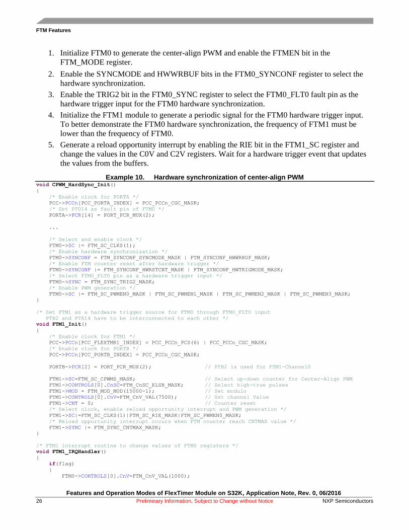
4.3.4. Updating FTM registers by hardware trigger—hardware
synchronization
The hardware synchronization is another way of updating the FTM registers when the counter is
running. In this case, the interrupt routine is not necessary because the FTM registers can be changed at
any time during the code execution and their values are updated as soon as a hardware trigger occurs.
The CPU load can be significantly reduced this way.
Three hardware trigger signal inputs of the FTM module can be selected depending on the enabled
TRIGn bit in the FTM_SYNC register. If TRIG0 is set, the hardware trigger source comes from many
other modules, such as LPIT and CMP (and other) through a flexible TRIGMUX module. By setting the
TRIG1 bit in the FTM_SYNC register, a hardware trigger is generated according to the
FTM0SYNCBIT bit in the SIM_FTMOPT1 register. In this section, the third option is demonstrated by
enabling the TRIG2 bit. In this case, the FTMx_FLT0 fault pin is chosen as the hardware trigger input
for the FTM hardware synchronization.
FTM Features
Features and Operation Modes of FlexTimer Module on S32K, Application Note, Rev. 0, 06/2016
26 Preliminary Information, Subject to Change without Notice NXP Semiconductors
1. Initialize FTM0 to generate the center-align PWM and enable the FTMEN bit in the
FTM_MODE register.
2. Enable the SYNCMODE and HWWRBUF bits in the FTM0_SYNCONF register to select the
hardware synchronization.
3. Enable the TRIG2 bit in the FTM0_SYNC register to select the FTM0_FLT0 fault pin as the
hardware trigger input for the FTM0 hardware synchronization.
4. Initialize the FTM1 module to generate a periodic signal for the FTM0 hardware trigger input.
To better demonstrate the FTM0 hardware synchronization, the frequency of FTM1 must be
lower than the frequency of FTM0.
5. Generate a reload opportunity interrupt by enabling the RIE bit in the FTM1_SC register and
change the values in the C0V and C2V registers. Wait for a hardware trigger event that updates
the values from the buffers.
Example 10. Hardware synchronization of center-align PWM void CPWM_HardSync_Init()
{
/* Enable clock for PORTA */
PCC->PCCn[PCC_PORTA_INDEX] = PCC_PCCn_CGC_MASK;
/* Set PTD14 as fault pin of FTM0 */
PORTA->PCR[14] = PORT_PCR_MUX(2);
...
/* Select and enable clock */
FTM0->SC |= FTM_SC_CLKS(1);
/* Enable hardware synchronization */
FTM0->SYNCONF = FTM_SYNCONF_SYNCMODE_MASK | FTM_SYNCONF_HWWRBUF_MASK;
/* Enable FTM counter reset after hardware trigger */
FTM0->SYNCONF |= FTM_SYNCONF_HWRSTCNT_MASK | FTM_SYNCONF_HWTRIGMODE_MASK;
/* Select FTM0_FLT0 pin as a hardware trigger input */
FTM0->SYNC = FTM_SYNC_TRIG2_MASK;
/* Enable PWM generation */
FTM0->SC |= FTM_SC_PWMEN0_MASK | FTM_SC_PWMEN1_MASK | FTM_SC_PWMEN2_MASK | FTM_SC_PWMEN3_MASK;
}
/* Set FTM1 as a hardware trigger source for FTM0 through FTM0_FLT0 input
PTB2 and PTA14 have to be interconnected to each other */
void FTM1_Init()
{
/* Enable clock for FTM1 */
PCC->PCCn[PCC_FLEXTMR1_INDEX] = PCC_PCCn_PCS(6) | PCC_PCCn_CGC_MASK;
/* Enable clock for PORTB */
PCC->PCCn[PCC_PORTB_INDEX] = PCC_PCCn_CGC_MASK;
PORTB->PCR[2] = PORT_PCR_MUX(2); // PTB2 is used for FTM1-Channel0
FTM1->SC=FTM_SC_CPWMS_MASK; // Select up-down counter for Center-Align PWM
FTM1->CONTROLS[0].CnSC=FTM_CnSC_ELSB_MASK; // Select high-true pulses
FTM1->MOD = FTM_MOD_MOD(15000-1); // Set modulo
FTM1->CONTROLS[0].CnV=FTM_CnV_VAL(7500); // Set channel Value
FTM1->CNT = 0; // Counter reset
/* Select clock, enable reload opportunity interrupt and PWM generation */
FTM1->SC|=FTM_SC_CLKS(1)|FTM_SC_RIE_MASK|FTM_SC_PWMEN0_MASK;
/* Reload opportunity interrupt occurs when FTM counter reach CNTMAX value */
FTM1->SYNC |= FTM_SYNC_CNTMAX_MASK;
}
/* FTM1 interrupt routine to change values of FTM0 registers */
void FTM1_IRQHandler()
{
if(flag)
{
FTM0->CONTROLS[0].CnV=FTM_CnV_VAL(1000);

FTM Features
Features and Operation Modes of FlexTimer Module on S32K, Application Note, Rev. 0, 06/2016
NXP Semiconductors Preliminary Information, Subject to Change without Notice 27
FTM0->CONTROLS[2].CnV=FTM_CnV_VAL(4000);
}
else
{
FTM0->CONTROLS[0].CnV=FTM_CnV_VAL(4000);
FTM0->CONTROLS[2].CnV=FTM_CnV_VAL(1000);
}
flag = !flag;
FTM1->SC &= ~FTM_SC_RF_MASK; // Clear Reload Flag bit
}
The resulting behavior of the code example is shown in this figure:
up-down counter period
up-down counter period
up-down counter period
hardware trigger (counter reset)
hardware trigger (counter reset)
hardware trigger (counter reset)
20% duty cycle
70% duty cycle 20% duty cycle
70% duty cycle
Figure 15. Hardware synchronization of center-align PWM
In Figure 15, the scope channels CH1, CH2, and CH3 represent the FTM0 module channels
FTM0_CH0, FTM0_CH1, and FTM0_CH2, respectively. FTM0_CH0 and FTM0_CH1 work in the
complementary mode, same as FTM0_CH2 and FTM0_CH3. Channel CH4 shows the hardware trigger
generated from FTM1 whose frequency is one third of the FTM0 frequency. After receiving the first
hardware trigger, the duty cycles of the channel pair FTM_CH0/FTM_CH1 and the channel pair
FTM_CH2/FTM_CH3 change from 20 % to 70 % and from 70 % to 20 %, respectively. The next
hardware trigger updates the new values of the C0V and C2V registers and the duty cycle of the
corresponding channel pair changes back to the previous value.

FTM Features
Features and Operation Modes of FlexTimer Module on S32K, Application Note, Rev. 0, 06/2016
28 Preliminary Information, Subject to Change without Notice NXP Semiconductors
4.4. Global Time Base (GTB)
There are multiple FTMs on the chip, but the multiple FTM modules are independent. If the application
requires more PWM channels than what one FTM can provide, multiple FTM modules can be used, but,
they must be synchronized. The synchronization of two (or more) FTM modules means that their
counters have the same values at any time instant.
The S32K device provides the GTB mechanism to synchronize multiple FTMs. The GTB is a
synchronous signal generated by the master FTM that launches the counter of all FTMs used. These two
conditions must be met when using the GTB function: each FTM must have the same clock source and
each FTM must start at the same time.
To enable the GTB feature, perform these steps for each participating FTM module:
1. Stop the FTM counter (write 00b to SC[CLKS]).
2. Program the FTM to the intended configuration. The FTM counter mode must be consistent
across all participating modules.
3. Write 1 to CONF[GTBEEN] and write 0 to CONF[GTBEOUT] at the same time.
4. Select the intended FTM counter clock source in SC[CLKS]. The clock source must be
consistent across all participating modules.
5. Reset the FTM counter (write any value to the CNT register).
The following example shows the synchronization of two generating FMTs—FTM0 and FTM2. The
duty cycles of both PWMs are adjusted to very low values to better demonstrate the functionality of the
GTB mechanism.
Example 11. Center-align PWM and GTB function
void CPWM_and_Global_Time_Base()
{
/* Enable clock for PORTD */
PCC->PCCn[PCC_PORTD_INDEX] = PCC_PCCn_CGC_MASK;
/* Select and enable clock for FTM0 */
PCC->PCCn[PCC_FLEXTMR0_INDEX] = PCC_PCCn_PCS(6) | PCC_PCCn_CGC_MASK;
/* Select and enable clock for FTM2 */
PCC->PCCn[PCC_FLEXTMR2_INDEX] = PCC_PCCn_PCS(6) | PCC_PCCn_CGC_MASK;
PORTD->PCR[15] = PORT_PCR_MUX(2); // Set PTD15 for FTM0 - Channel0
PORTD->PCR[16] = PORT_PCR_MUX(2); // Set PTD16 for FTM0 - Channel1
PORTD->PCR[0] = PORT_PCR_MUX(4); // Set PTD0 for FTM2 - Channel0
PORTD->PCR[1] = PORT_PCR_MUX(4); // Set PTD1 for FTM2 - Channel1
/* Select up-down counter for Center-Align PWM */
FTM0->SC = FTM_SC_CPWMS_MASK;
FTM2->SC = FTM_SC_CPWMS_MASK;
/* Enable registers updating from write buffers */
FTM0->MODE = FTM_MODE_FTMEN_MASK;
FTM2->MODE = FTM_MODE_FTMEN_MASK;
/* Enable complementary mode for channels pair n=1 */
FTM0->COMBINE = FTM_COMBINE_COMP0_MASK;
FTM2->COMBINE = FTM_COMBINE_COMP0_MASK;
/* Set Modulo (10kHz PWM frequency @112MHz system clock) */
FTM0->MOD = FTM_MOD_MOD(5600-1);
FTM2->MOD = FTM_MOD_MOD(5600-1);
/* Set CNTIN */
FTM0->CNTIN = FTM_CNTIN_INIT(0);
FTM2->CNTIN = FTM_CNTIN_INIT(0);
/* High-true pulses of PWM signals */

FTM Features
Features and Operation Modes of FlexTimer Module on S32K, Application Note, Rev. 0, 06/2016
NXP Semiconductors Preliminary Information, Subject to Change without Notice 29
FTM0->CONTROLS[0].CnSC = FTM_CnSC_ELSB_MASK;
FTM0->CONTROLS[1].CnSC = FTM_CnSC_ELSB_MASK;
FTM2->CONTROLS[0].CnSC = FTM_CnSC_ELSB_MASK;
FTM2->CONTROLS[1].CnSC = FTM_CnSC_ELSB_MASK;
/* Set Channel Value – 1% duty cycle */
FTM0->CONTROLS[0].CnV=FTM_CnV_VAL(56);
FTM2->CONTROLS[0].CnV=FTM_CnV_VAL(56);
/* FTM counter reset */
FTM0->CNT = 0;
FTM2->CNT = 0;
/* Enable global time base to control FTM0 and FTM2 */
FTM0->CONF = FTM_CONF_GTBEEN_MASK;
FTM2->CONF = FTM_CONF_GTBEEN_MASK;
/* Select clock */
FTM0->SC |= FTM_SC_CLKS(1);
FTM2->SC |= FTM_SC_CLKS(1);
/* Synchronization signal for FTM0 and FTM2 */
FTM0->CONF |= FTM_CONF_GTBEOUT_MASK;
/* Enable PWM generation */
FTM0->SC |= FTM_SC_PWMEN0_MASK | FTM_SC_PWMEN1_MASK;
FTM2->SC |= FTM_SC_PWMEN0_MASK | FTM_SC_PWMEN1_MASK;
}
The center-align PWMs of FTM0 and FTM2 with no GTB activated and with the GTB activated are
shown in these two figures:
1% duty-cycle of FTM0
1% duty-cycle of FTM2
Up-down counters of FTM0 and FTM2 are not synchronized by GTB
Figure 16. Center–align PWM with no GTB activated

FTM Features
Features and Operation Modes of FlexTimer Module on S32K, Application Note, Rev. 0, 06/2016
30 Preliminary Information, Subject to Change without Notice NXP Semiconductors
1% duty-cycle of FTM0
1% duty-cycle of FTM2
Up-down counters of FTM0 and FTM2 are synchronized by GTB
Figure 17. Center–align PWM with GTB activated
In Figure 16 and Figure 17, the scope channels CH1, CH2, CH3, and CH4 represent the FTM0 and
FTM2 modules’ channels FTM0_CH0, FTM0_CH1, FTM2_CH0, and FTM2_CH1, respectively.
FTM0_CH0 and FTM0_CH1 work in the complementary mode, same as FTM2_CH0 and FTM2_CH1.
The time base of the scope is adjusted so that a 1 % duty cycle of channels FTM0 and FTM2 can be
clearly seen on the scope display. If the global time base is not activated, the up-down counters of the
FTMs used are not perfectly aligned to each other, neither are their channel signals (see Figure 16). Such
problem is handled by applying the GTB function to the FTM modules (see Figure 17).
NOTE
The GTB feature does not provide a continuous synchronization of the
FTM counters, meaning that the FTM counters may lose the
synchronization during the FTM operation. The GTB feature only enables
the FTM counters to start their operation synchronously.
4.5. ADC triggering by FTM and PDB modules
In motor-control applications, as well as in switched-mode power supply applications, it is necessary to
measure the currents at the center of the PWM signal. The power devices do not switch at this time
instant, therefore the voltage drop sensed on the shunt resistor is stable.
All four FTM modules of the S32K device have up to eight channels. Six channels are usually enough to
generate the PWM signals necessary to control commonly used 3-phase motors. The remaining two
channels of the FTM module can then be used to control the instant of the ADC conversions.

FTM Features
Features and Operation Modes of FlexTimer Module on S32K, Application Note, Rev. 0, 06/2016
NXP Semiconductors Preliminary Information, Subject to Change without Notice 31
The triggering signal of the FTM module can be selected in the FTM_EXTTRIG register. All FTM
channels can be used to trigger the ADC module. For example, if CH0 is set in the FTM_EXTTRIG
register, the FTM counter counts until it reaches the value written in the C0V register. At this time
instant, CH0 generates a signal that triggers the ADC module on every FTM counter period. If the
INITTRIG bit is set in the FTM_EXTTRIG register, the trigger signal is generated every time the FTM
counter reaches the value of the CNTIN register.
The default and suggested hardware triggering scheme for the ADC module is through the
Programmable Delay Block (PDB). The current implementation of the S32K device is equipped with
two ADC modules and two PDB modules that work in pairs. This means that PDB0 is linked with
ADC0 and PDB1 is linked with ADC1. Each PDB module can be triggered either by software or
hardware. The FTM module is one of the trigger sources that can be enabled through the TRGMUX
registers TRGMUX_PDB0 and TRGMUX_PDB1.
To generate the center-align PWM and to trigger ADC0 by FTM0 through PDB0, perform these steps:
1. Initialize the FTM0 module to generate the center-align PWM and enable the INITTRIGEN bit
in the FTM0_EXTTRIG register to generate a hardware trigger for the ADC0 module.
2. Configure the TRGMUX module to trigger ADC0 by FTM0 through the PDB0 module by
writing 0x16 to the SEL0 bit field in the TRGMUX_PDB0 register.
3. Delay the FTM0 initialization trigger by the PDB0 block to trigger ADC0 at the center of the
PWM cycle by writing appropriate values into the PDB0_MOD and PDB0_CH0DLY0 registers.
4. Initialize the ADC0 module and enable the ADTRG bit in the ADC0_SC2 register to trigger
ADC0 by the FTM0 module.
The following code example demonstrates the configuration of the FTM0, PDB0, and ADC0 modules,
where FTM0 is used to generate the center-align PWM and to trigger ADC0 through the PDB0 module.
Example 12. ADC triggering by FTM and PDB modules /* FTM0 Initialization */
void FTM0_Init()
{
/* Enable clock for PORTD */
PCC->PCCn[PCC_PORTD_INDEX] = PCC_PCCn_CGC_MASK;
/* Select and enable clock for FTM0 */
PCC->PCCn[PCC_FLEXTMR0_INDEX] = PCC_PCCn_PCS(6) | PCC_PCCn_CGC_MASK;
PORTD->PCR[15] = PORT_PCR_MUX(2); // Set PTD15 for FTM0 – Channel0
PORTD->PCR[16] = PORT_PCR_MUX(2); // Set PTD16 for FTM0 – Channel1
PORTD->PCR[0] = PORT_PCR_MUX(2); // Set PTD0 for FTM0 – Channel2
PORTD->PCR[1] = PORT_PCR_MUX(2); // Set PTD1 for FTM0 – Channel3
PORTD->PCR[2] = PORT_PCR_MUX(1); // Set PTD2 as a PTD2
PORTD->PCR[3] = PORT_PCR_MUX(1); // Set PTD3 as a PTD3
PTD->PDDR = (1<<2) | (1<<3); // Set PTD2 and PTD3 as an output
/* Select up-down counter for Center-Align PWM */
FTM0->SC = FTM_SC_CPWMS_MASK;
/* Enable combine, complementary mode and dead-time for channels pair CH0/CH1 and CH2/CH3 */
FTM0->COMBINE = FTM_COMBINE_SYNCEN0_MASK | FTM_COMBINE_COMP0_MASK | FTM_COMBINE_DTEN0_MASK;
FTM0->COMBINE |= FTM_COMBINE_SYNCEN1_MASK | FTM_COMBINE_COMP1_MASK | FTM_COMBINE_DTEN1_MASK;
/* Set Modulo (10kHz PWM frequency @112MHz system clock) */
FTM0->MOD = FTM_MOD_MOD(5600-1);
/* Set CNTIN */
FTM0->CNTIN = FTM_CNTIN_INIT(0);
/* High-true pulses of PWM signals */
FTM0->CONTROLS[0].CnSC = FTM_CnSC_ELSB_MASK;
FTM0->CONTROLS[1].CnSC = FTM_CnSC_ELSB_MASK;
FTM0->CONTROLS[2].CnSC = FTM_CnSC_ELSB_MASK;
FTM0->CONTROLS[3].CnSC = FTM_CnSC_ELSB_MASK;

FTM Features
Features and Operation Modes of FlexTimer Module on S32K, Application Note, Rev. 0, 06/2016
32 Preliminary Information, Subject to Change without Notice NXP Semiconductors
/* Set Channel Value */
FTM0->CONTROLS[0].CnV=FTM_CnV_VAL(2800); // 50% duty cycle
FTM0->CONTROLS[1].CnV=FTM_CnV_VAL(2800); // 50% duty cycle
FTM0->CONTROLS[2].CnV=FTM_CnV_VAL(2800); // 50% duty cycle
FTM0->CONTROLS[3].CnV=FTM_CnV_VAL(2800); // 50% duty cycle
/* FTM counter reset */
FTM0->CNT = 0;
/* Insert DeadTime (1us) */
FTM0->DEADTIME = FTM_DEADTIME_DTPS(3) | FTM_DEADTIME_DTVAL(7);
/* Enable trigger generation when FTM counter = CNTIN */
FTM0->EXTTRIG = FTM_EXTTRIG_INITTRIGEN_MASK;
/* Enable clock and PWM */
FTM0->SC |= FTM_SC_CLKS(1) | FTM_SC_PWMEN0_MASK | FTM_SC_PWMEN1_MASK | FTM_SC_PWMEN2_MASK|
FTM_SC_PWMEN3_MASK;
}
/* PDB0 Initialization */
void PDB0_Init()
{
PCC->PCCn[PCC_PDB0_INDEX] = PCC_PCCn_CGC_MASK; // Enable clock for PDB0
FSL_NVIC->ISER[PDB0_IRQn / 32] |= (1 << (PDB0_IRQn % 32)); // Enable interrupt
PDB0->MOD = 11200; // Set Modulo
PDB0->CH[0].C1 = PDB_C1_TOS(1) | PDB_C1_EN(1); // Select and enable Channel0
PDB0->CH[0].DLY[0] = 5600; // Set delay
PDB0->IDLY = 0; // Set interrupt delay
PDB0->SC |= PDB_SC_PRESCALER(0) | PDB_SC_MULT(0); // Select clock prescaler and mult factor
/* Select trigger input source and enable interrupt */
PDB0->SC |= PDB_SC_TRGSEL(0) | PDB_SC_PDBIE_MASK;
/* Enable PDB and update PDB registers */
PDB0->SC |= PDB_SC_PDBEN_MASK | PDB_SC_LDOK_MASK;
}
/* TRGMUX Initialization */
void TRGMUX_Init()
{
PCC->PCCn[PCC_TRGMUX_INDEX] = PCC_PCCn_CGC_MASK; // Enable clock for TRGMUX module
/* Set FTM as a trigger source for PDB0 */
TRGMUX->TRGMUXn[TRGMUX_PDB0_INDEX] = TRGMUX_TRGMUXn_SEL0(0x16);
}
void ADC0_Init()
{
PCC->PCCn[PCC_ADC0_INDEX] = 0; // Disable clock for ADC0
PCC->PCCn[PCC_ADC0_INDEX] = PCC_PCCn_PCS(6) | PCC_PCCn_CGC_MASK; // Enable clock for ADC0
FSL_NVIC->ISER[ADC0_IRQn / 32] |= (1 << (ADC0_IRQn % 32)); // Enable interrupt
/* Set divide ratio to 1 and select 8-bit conversion */
ADC0->CFG1 = ADC_CFG1_ADIV(0) | ADC_CFG1_MODE(0) | ADC_CFG1_ADICLK(0);
/* Select hardware trigger */
ADC0->SC2 = ADC_SC2_ADTRG_MASK;
/* Select channel 12 as an input and enable conversion complete interrupt */
ADC0->SC1[0] = ADC_SC1_AIEN_MASK | ADC_SC1_ADCH(12);
}
/* ADC0 interrupt routine */
void ADC0_IRQHandler()
{
PTD->PTOR |= 1<<3; // Toggle PTD2 to show completed ADC conversions
ADC0_RA = ADC0->R[0]; // Read ADC result register
}
/* PDB0 interrupt routine */
void PDB0_IRQHandler()
{
PTD->PTOR |= 1<<2; // Toggle PTD2 to show FTM0 trigger signal
PDB0->SC &= ~PDB_SC_PDBIF_MASK; // Clear PDB interrupt flag
}

Revision History
Features and Operation Modes of FlexTimer Module on S32K, Application Note, Rev. 0, 06/2016
NXP Semiconductors Preliminary Information, Subject to Change without Notice 33
The resulting behavior of the code example is shown in this figure:
FTM0_CH0
FTM0_CH1
ADC Conversion complete (COCO=1)
FTM trigger generated when FTM counter = CNTIN
Up-counter period PDB delay ADC conversion delay
Figure 18. ADC triggering by FTM and PDB modules
In Figure 18, the scope channels CH1 and CH2 represent the FTM0 channels FTM0_CH0 and
FTM0_CH1, respectively. The channel pair FTM0_CH0/FTM0_CH1 works in the complementary
mode, same as the channel pair FTM0_CH2/FTM0_CH3. The scope channels CH3 and CH4
demonstrate the interconnection between the FTM0, PDB0, and ADC0 modules. While channel CH3
represents the PTD2 pin toggling in the PDB0 interrupt routine every time the FTM0 counter reaches the
value of the CNTIN register, channel CH4 displays the PTD3 pin toggling in the ADC0 interrupt routine
every time the ADC0 conversion is completed (COCO = 1). The FTM0 trigger signal is delayed by the
PDB0 module so that the ADC0 conversion occurs at the center of the PWM signal.
5. Revision History
This table summarizes the changes done to the document since the initial release:
Table 5. Revision history
Revision number Date Substantive changes
0 06/2016 Initial release.

Document Number: AN5303 Rev. 0
06/2016
How to Reach Us:
Home Page:
nxp.com
Web Support:
nxp.com/support
Information in this document is provided solely to enable system and software
implementers to use NXP products. There are no express or implied copyright licenses
granted hereunder to design or fabricate any integrated circuits based on the
information in this document. NXP reserves the right to make changes without further
notice to any products herein.
NXP makes no warranty, representation, or guarantee regarding the suitability of its
products for any particular purpose, nor does NXP assume any liability arising out of the
application or use of any product or circuit, and specifically disclaims any and all
liability, including without limitation consequential or incidental damages. “Typical”
parameters that may be provided in NXP data sheets and/or specifications can and do
vary in different applications, and actual performance may vary over time. All operating
parameters, including “typicals,” must be validated for each customer application by
customer’s technical experts. NXP does not convey any license under its patent rights
nor the rights of others. NXP sells products pursuant to standard terms and conditions
of sale, which can be found at the following address:
nxp.com/SalesTermsandConditions.
NXP, the NXP logo, NXP SECURE CONNECTIONS FOR A SMARTER WORLD,
Kinetis, Vybrid, Freescale, and the Freescale logo are trademarks of NXP B.V. All other
product or service names are the property of their respective owners.
© 2016 NXP B.V.
Preliminary Information, Subject to Change without Notice