features descriptio u u electrical characteristics consult ltc marketing for parts specified with...
TRANSCRIPT
1
LTC1530
1530fa
The LTC®1530 is a high power synchronous switchingregulator controller optimized for 5V to 1.3V-3.5V outputapplications. Its synchronous switching architecture drivestwo external N-channel MOSFET devices to provide highefficiency. The LTC1530 contains a precision trimmedreference and feedback system that provides worst-caseoutput voltage regulation of ±2% over temperature, loadcurrent and line voltage shifts. Current limit circuitrysenses the output current through the on-resistance ofthe topside N-channel MOSFET, providing an adjustablecurrent limit without requiring an external low value senseresistor.
The LTC1530 includes a fixed frequency PWM oscillatorthat free runs at 300kHz, providing greater than 90%efficiency in converter designs from 1A to 20A of outputcurrent. Shutdown mode drops the LTC1530 supply cur-rent to 45µA.
The LTC1530 is specified for commercial and industrialtemperature ranges and is available in the S0-8 package.
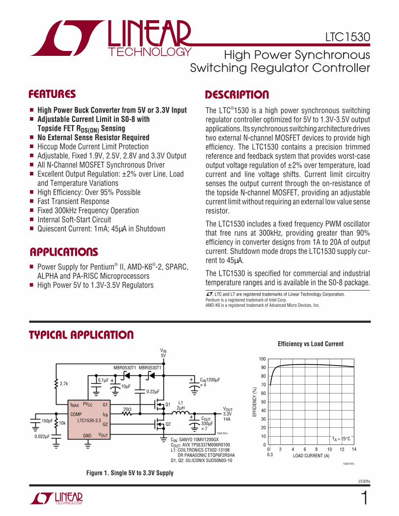
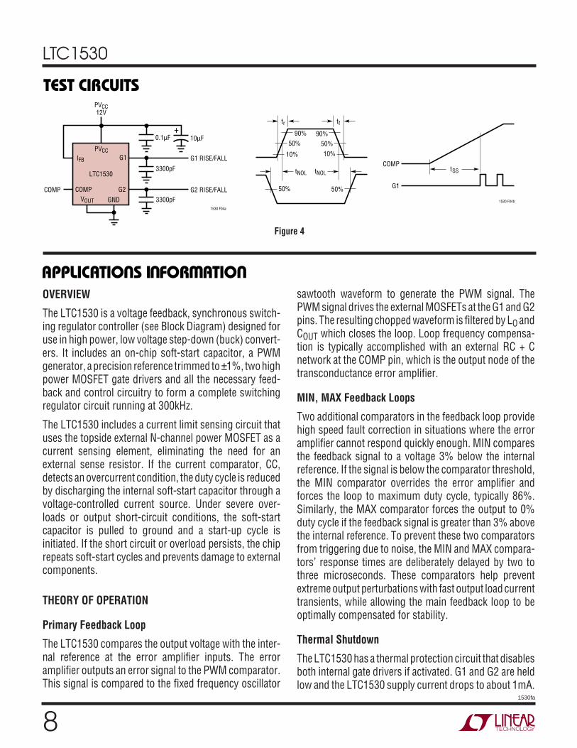
Figure 1. Single 5V to 3.3V Supply
LOAD CURRENT (A)00.3
EFFI
CIEN
CY (%
)
100
90
80
70
60
50
40
30
20
10
04 8 10
1530 F01b
2 6 12 14
TA = 25°C
Efficiency vs Load Current
High Power Buck Converter from 5V or 3.3V Input Adjustable Current Limit in S0-8 with
Topside FET RDS(ON) Sensing No External Sense Resistor Required Hiccup Mode Current Limit Protection Adjustable, Fixed 1.9V, 2.5V, 2.8V and 3.3V Output All N-Channel MOSFET Synchronous Driver Excellent Output Regulation: ±2% over Line, Load
and Temperature Variations High Efficiency: Over 95% Possible Fast Transient Response Fixed 300kHz Frequency Operation Internal Soft-Start Circuit Quiescent Current: 1mA; 45µA in Shutdown
Power Supply for Pentium® II, AMD-K6®-2, SPARC,ALPHA and PA-RISC Microprocessors
High Power 5V to 1.3V-3.5V Regulators
+ +2.7k
0.1µF10µF
+ COUT330µF× 7
CIN1200µF× 4
L12µH
MBR0530T1 MBR0530T1
20ΩPVCC
GND
LTC1530-3.3
G1
COMP IFB
IMAX
G2
VOUT
VOUT3.3V14A
1530 F01a
VIN5V
CIN: SANYO 10MV1200GXCOUT: AVX TPSE337M006R0100L1: COILTRONICS CTX02-13198 OR PANASONIC ETQP6F2R5HAQ1, Q2: SILICONIX SUD50N03-10
10k
0.022µF
0.22µF
Q1
Q2150pF
, LTC and LT are registered trademarks of Linear Technology Corporation.Pentium is a registered trademark of Intel Corp.AMD-K6 is a registered trademark of Advanced Micro Devices, Inc.
DESCRIPTIO
U
FEATURES
APPLICATIO SU
TYPICAL APPLICATIO
U
High Power SynchronousSwitching Regulator Controller
2
LTC1530
1530fa
ORDER PARTNUMBER
LTC1530CS8LTC1530CS8-1.9LTC1530CS8-2.5LTC1530CS8-2.8LTC1530CS8-3.3LTC1530IS8LTC1530IS8-1.9LTC1530IS8-2.5LTC1530IS8-2.8LTC1530IS8-3.3
S8 PART MARKING
TJMAX = 125°C, θJA = 130°C/ W
*VOUT FOR FIXED VOLTAGE VERSIONS
TOP VIEW
G1
G2
IFB
IMAX
PVCC
GND
S8 PACKAGE8-LEAD PLASTIC SO
1
2
3
4
8
7
6
5
*VSENSE/VOUT
COMP
1530153019153025
530I28530I33
1530I530I19530I25
(Note 1)
Supply VoltagePVCC ........................................................................ 14VInput Voltage IFB (Note 2) ............................................... PVCC + 0.3V IMAX ........................................................ –0.3V to 14VIFB Input Current (Notes 2,3) ............................ –100mAOperating Ambient Temperature Range
LTC1530C ............................................... 0°C to 70°CLTC1530I ............................................ –40°C to 85°C
Maximum Junction TemperatureLTC1530C, LTC1530I ...................................... 125°C
Storage Temperature Range ................. –65°C to 150°CLead Temperature (Soldering, 10 sec).................. 300°C
153028153033
The denotes specifications that apply over the full operating temperaturerange, otherwise specifications are at TA = 25°C. PVCC = 12V unless otherwise noted. (Note 3)
SYMBOL PARAMETER CONDITIONS MIN TYP MAX UNITS
VSENSE Internal Feedback Voltage LTC1530CS8 (Note 4) 1.223 1.235 1.247 V 1.216 1.235 1.254 V
VOUT Output Voltage LTC1530CS8-1.9 (Note 4) 1.881 1.9 1.919 V 1.871 1.9 1.929 V
LTC1530CS8-2.5 (Note 4) 2.475 2.5 2.525 V 2.462 2.5 2.538 V
LTC1530CS8-2.8 (Note 4) 2.772 2.8 2.828 V 2.758 2.8 2.842 V
LTC1530CS8-3.3 (Note 4) 3.267 3.3 3.333 V 3.250 3.3 3.350 V
gmERR Error Amplifier Transconductance (Note 5) 1.6 2 2.6 millimho
The denotes specifications that apply over the full operating temperature range, otherwise specifications are at TA = 25°C.PVCC = 12V unless otherwise noted. (Note 3)SYMBOL PARAMETER CONDITIONS MIN TYP MAX UNITS
PVCC Supply Voltage (Note 6) 13.2 V
VUVLO Undervoltage Lockout Voltage (Note 7) 3.5 3.75 V
VSENSE Internal Feedback Voltage LTC1530IS8 (Note 4) 1.223 1.235 1.247 V 1.210 1.235 1.260 V
PACKAGE/ORDER I FOR ATIOU UW
ABSOLUTE AXI U RATI GS
W WW U
ELECTRICAL CHARACTERISTICS
Consult LTC Marketing for parts specified with wider operating temperature ranges.
3
LTC1530
1530fa
SYMBOL PARAMETER CONDITIONS MIN TYP MAX UNITS
VOUT Output Voltage LTC1530IS8-1.9 (Note 4) 1.881 1.9 1.919 V 1.862 1.9 1.938 V
LTC1530IS8-2.5 (Note 4) 2.475 2.5 2.525 V 2.450 2.5 2.550 V
LTC1530IS8-2.8 (Note 4) 2.772 2.8 2.828 V 2.744 2.8 2.856 V
LTC1530IS8-3.3 (Note 4) 3.267 3.3 3.333 V 3.234 3.3 3.366 V
∆VOUT Output Load Regulation IOUT = 0 to 14A –5 mV
Output Line Regulation VIN = 4.75V to 5.25V, IOUT = 0 ±1 mV
IPVCC Operating Supply Current Figure 3, VFB = 0V (Note 8) 15 mA
Quiescent Current Figure 3, COMP = 0.5V, VFB = 5V 1.0 1.4 mA
Shutdown Supply Current Figure 3, COMP = 0 (Note 9) 45 80 µA
fOSC Internal Oscillator Frequency Figure 4 250 300 350 kHz
Oscillator Valley Voltage VCOMP at 0% Duty Cycle 2.5 V
Oscillator Peak Voltage VCOMP at Max Duty Cycle 3.5 V
GERR Error Amplifier Open-Loop DC Gain (Note 5) 40 54 dB
gmERR Error Amplifier Transconductance (Note 5) 1.6 2 2.8 millimho
IMAX IMAX Sink Current VIMAX = 5V 170 200 230 µAVIMAX = 5V 120 200 300 µA
IMAX Sink Current Tempco VIMAX = 5V 3300 ppm/°C
VSHDN Shutdown Threshold Voltage Figure 4, Measured at COMP Pin (Note 9) 100 180 mV
SRSS Internal Soft-Start Slew Rate Figure 4, COMP Pulls High, VFB = 0V 0.4 V/ms(Notes 9, 10)
tSS Internal Soft-Start Wake-Up Time Figure 4, COMP Pulls High to G1↑ (Note 10) 3.5 ms
tr, t f Driver Rise and Fall Time Figure 4 90 140 ns
tNOL Driver Nonoverlap Time Figure 4 30 100 ns
DCMAX Maximum G1 Duty Cycle Figure 4 81 86 %
Note 1: Absolute Maximum Ratings are those values beyond which the lifeof a device may be impaired.Note 2: If IFB is taken below GND, it is clamped by an internal diode. Thispin handles input currents ≤ 100mA below GND without latch-up. In thepositive direction, it is not clamped to PVCC.Note 3: All currents into device pins are positive; all currents out of devicepins are negative. All voltages are referenced to ground unless otherwisespecified.Note 4: The LTC1530 is tested in an op amp feedback loop whichregulates VSENSE or VOUT based on VCOMP = 2V for the error amplifier.Note 5: The Open-loop DC gain and transconductance from the VFB pin tothe COMP pin are GERR and gmERR respectively. For fixed output voltageversions, the actual open-loop DC gain and transconductance are GERRand gmERR multiplied by the ratio 1.235/VOUT.
Note 6: The total voltage from the PVCC pin to the GND pin must be ≥8Vfor the current limit protection circuit to be active.Note 7: G1 and G2 begin to switch once PVCC is ≥ the undervoltagelockout threshold voltage.Note 8: Supply current in normal operation is dominated by the currentneeded to charge and discharge the external FET gates. This current varieswith the LTC1530 operating frequency, supply voltage and the externalFETs used.Note 9: The LTC1530 enters shutdown if COMP is pulled low.Note 10: Slew rate is measured at the COMP pin on the transition fromshutdown to active mode.
The denotes specifications that apply over the full operating temperaturerange, otherwise specifications are at TA = 25°C. PVCC = 12V unless otherwise noted. (Note 3)ELECTRICAL CHARACTERISTICS
4
LTC1530
1530fa
OUTPUT CURRENT (A)
2.510
2.508
2.506
2.504
2.502
2.500
2.498
2.496
2.494
2.492
2.490
OUTP
UT V
OLTA
GE (V
)
1530 G02
0 1 2 3 4 5 6
TA = 25°CREFER TO FIGURE 2
Efficiency vs Load Current Load Regulation
LOAD CURRENT (A)00.3
EFFI
CIEN
CY (%
)
100
90
80
70
60
50
40
30
20
10
04 8 10
1530 G01
2 6 12 14
TA = 25°CREFER TO FIGURE 10
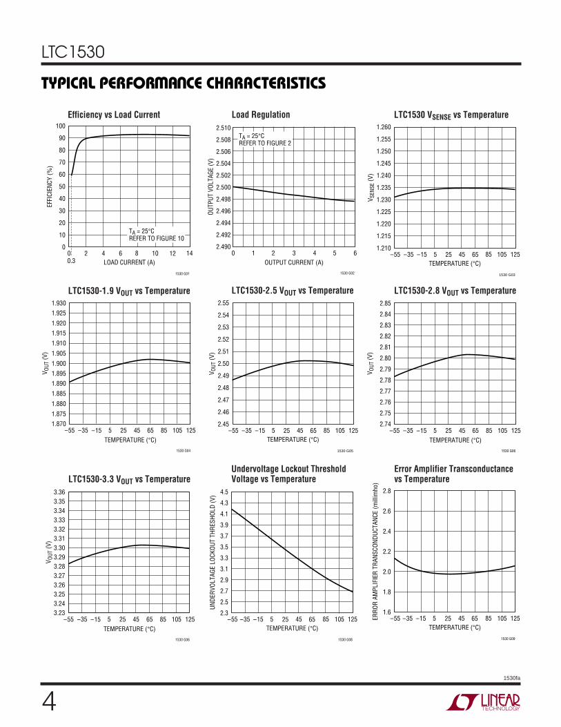
TYPICAL PERFOR A CE CHARACTERISTICS
UW
LTC1530 VSENSE vs Temperature
TEMPERATURE (°C)–55
V SEN
SE (V
)
1.260
1.255
1.250
1.245
1.240
1.235
1.230
1.225
1.220
1.215
1.210–15 25 45 125
1530 G03
–35 5 65 85 105
LTC1530-1.9 VOUT vs Temperature LTC1530-2.5 VOUT vs Temperature
TEMPERATURE (°C)–55
V OUT
(V)
1.9301.925
1.9201.915
1.910
1.905
1.900
1.895
1.890
1.885
1.880
1.875
1.87025
1530 G04
–35 –15 5 45 65 85 105 125TEMPERATURE (°C)
–55
V OUT
(V)
2.55
2.54
2.53
2.52
2.51
2.50
2.49
2.48
2.47
2.46
2.45–15 25 45 125
1530 G05
–35 5 65 85 105
Undervoltage Lockout ThresholdVoltage vs Temperature
LTC1530-2.8 VOUT vs Temperature
TEMPERATURE (°C)–55
V OUT
(V)
2.85
2.84
2.83
2.82
2.81
2.80
2.79
2.78
2.77
2.76
2.75
2.7425
1530 G06
–35 –15 5 45 65 85 105 125
LTC1530-3.3 VOUT vs Temperature
TEMPERATURE (°C)–55
V OUT
(V)
3.363.353.343.333.323.313.303.293.283.273.263.253.243.23
25
1530 G06
–35 –15 5 45 65 85 105 125
Error Amplifier Transconductancevs Temperature
TEMPERATURE (°C)–55
UNDE
RVOL
TAGE
LOC
KOUT
THR
ESHO
LD (V
) 4.5
4.3
4.1
3.9
3.7
3.5
3.3
3.1
2.9
2.7
2.5
2.3–15 25 45 125
1530 G08
–35 5 65 85 105TEMPERATURE (°C)
–55ERRO
R AM
PLIF
IER
TRAN
SCON
DUCT
ANCE
(mill
imho
)
2.8
2.6
2.4
2.2
2.0
1.8
1.6–15 25 45 125
1530 G09
–35 5 65 85 105

5
LTC1530
1530fa
PVCC Shutdown Supply Currentvs Temperature
PVCC Supply Currentvs Gate Capacitance
Shutdown Threshold Voltagevs Temperature Output Overcurrent Protection Transient Response
50µs/DIV 1530 G18
2A/DIV
50mV/DIV
Error Amplifier Open-Loop Gainvs Temperature
Oscillator Frequencyvs Temperature
Maximum G1 Duty Cyclevs Ambient Temperature
IMAX Sink Current vs Temperature
TEMPERATURE (°C)–55
ERRO
R AM
PLIF
IER
OPEN
-LOO
P DC
GAI
N (d
B)
60
55
50
45
40–15 25 45 125
1530 G10
–35 5 65 85 105TEMPERATURE (°C)
–55
OSCI
LLAT
OR F
REQU
ENCY
(kHz
)
350
340
330
320
310
300
290
280
270
260
250–15 25 45 125
1530 G11
–35 5 65 85 105AMBIENT TEMPERATURE (°C)
–55
MAX
IMUM
G1
DUTY
CYC
LE (%
)
92
90
88
86
84
82
80
78–15 25 45 125
1530 G12
–35 5 65 85 105
THERMAL SHUTDOWN OCCURSBEYOND THESE POINTS
G1, G2CAPACITANCE
= 1000pF
PVCC = 12VfOSC = 300kHz
7700pF5500pF
3300pF
2200pF
TEMPERATURE (°C)–55
I MAX
SIN
K CU
RREN
T (µ
A)
300
280
260
240
220
200
180
160
140
120–15 25 45 125
1530 G13
–35 5 65 85 105
PVCC = 12VG1, G2 ARE NOT SWITCHING
GATE CAPACITANCE (nF)0
PVCC
SUP
PLY
CURR
ENT
(mA)
6
1530 G14
2 4 8
70
60
50
40
30
20
10
01 3 5 7
PVCC = 12VTA = 25°CGATE CAPACITANCE = CG1 = CG2
TEMPERATURE (°C)–55
80
75
70
65
60
55
50
45
40
35
30–15 25 45 125
1530 G15
–35 5 65 85 105
PVCC = 12V
PVCC
SHU
TDOW
N CU
RREN
T (µ
A)
OUTPUT CURRENT (A)0
OUTP
UT V
OLTA
GE (V
)
3.0
2.5
2.0
1.5
1.0
0.5
08
1530 G17
21 3 5 7 94 6 10
SHORT-CIRCUITCURRENT
PVCC = 12VTA = 25°CREFER TOFIGURE 2
TEMPERATURE (°C)–55
SHUT
DOW
N TH
RESH
OLD
VOLT
AGE
(mV)
250
200
150
100
50
0–15 25 45 125
1530 G16
–35 5 65 85 105
PVCC = 12VMEASURED ATCOMP PIN
TYPICAL PERFOR A CE CHARACTERISTICS
UW

6
LTC1530
1530fa
COMP to compensate the feedback loop for optimumtransient response. To shut down the LTC1530, pull thispin below 0.1V with an open-collector or open-draintransistor. Supply current is typically reduced to 45µA inshutdown. An internal 4µA pullup ensures start-up.
IMAX (Pin 5): Current Limit Threshold. Current limit is setby the voltage drop across an external resistor connectedbetween the drain of Q1 and IMAX. This voltage is com-pared with the voltage across the RDS(ON) of the high sideMOSFET. The LTC1530 contains a 200µA internal pull-down at IMAX to set current limit. This 200µA currentsource has a positive temperature coefficient to providefirst order correction for the temperature coefficient of theexternal N-channel MOSFET’s RDS(ON).
IFB (Pin 6): Current Limit Sense Pin. Connect IFB to theswitching node between Q1’s source and Q2’s drain. If IFBdrops below IMAX with G1 on, the LTC1530 enters currentlimit. Under this condition, the internal soft-start capacitoris discharged and COMP is pulled low slowly. Duty cycleis reduced and output power is limited. The current limitcircuitry is only activated if PVCC ≥ 8V. This action easesstart-up considerations as PVCC is ramping up becausethe MOSFET’s RDS(ON) can be significantly higher thanwhat is measured under normal operating conditions. Thecurrent limit circuit is disabled by floating IMAX and short-ing IFB to PVCC.
G2 (Pin 7): Gate Drive for the Low Side N-Channel MOSFET,Q2. This output swings from PVCC to GND. It is always lowif G1 is high or if the output is disabled. To preventundershoot during a soft-start cycle, G2 is held low untilG1 first transitions high.
G1 (Pin 8): Gate Drive for the Topside N-Channel MOSFET,Q1. This output swings from PVCC to GND. It is always lowif G2 is high or if the output is disabled.
PVCC (Pin 1): Power Supply for G1, G2 and Logic. PVCCmust connect to a potential of at least VIN + VGS(ON)Q1. IfVIN = 5V, generate PVCC using a simple charge pumpconnected to the switching node between Q1 and Q2 (seeFigure 1) or connect PVCC to a 12V supply. Bypass PVCCproperly or erratic operation will result. A low ESR 10µFcapacitor or larger bypass capacitor along with a 0.1µFsurface mount ceramic capacitor in parallel is recom-mended from PVCC directly to GND to minimize switchingripple. Switching ripple should be ≤100mV at the PVCCpin.
GND (Pin 2): Power and Logic Ground. GND is connectedto the internal gate drive circuitry and the feedback cir-cuitry. To obtain good output voltage regulation, useproper ground techniques between the LTC1530 GND andbottom-side FET source and the negative terminal of theoutput capacitor. See the Applications Information sectionfor more details on PCB layout techniques.
VSENSE/VOUT (Pin 3): Feedback Voltage Pin. For the adjust-able LTC1530, use an external resistor divider to set therequired output voltage. Connect the tap point of theresistor divider network to VSENSE and the top of thedivider network to the output voltage. For fixed outputvoltage versions of the LTC1530, the resistor divider isinternal and the top of the resistor divider network isbrought out to VOUT. In general, the resistor dividernetwork for each fixed output voltage version sinks ap-proximately 30µA. Connect VOUT to the output voltageeither at the output capacitors or at the actual point of load.VSENSE/VOUT is sensitive to switching noise injected intothe pin. Isolate high current switching traces from this pinand its PCB trace.
COMP (Pin 4): External Compensation. The COMP pin isconnected to the error amplifier output and the input of thePWM comparator. An RC + C network is typically used at
UUU
PI FU CTIO S
7
LTC1530
1530fa
Figure 2 Figure 3
PVCC12V
VIN5V
Q1Si4410DY
LO*2.4µH
*SUMIDA CDRH127-2R4 **AVX TPSE337M006R0100***SANYO 10MV1200GX
+
Q2Si4410DY
RC8.2k
750Ω
100Ω
CC0.01µF
0.1µF 10µF
+
+ CO**330µF× 8
CIN***1200µF× 2
VOUT2.5V6A
1530 F02
C1100pF
IMAXPVCC
GND
G1
IFB
G2
VOUT
COMPLTC1530-2.5
+0.1µF10µF
1530 F03
IMAX
PVCC
PVCC12V
GND
G1 NC
NC
NC
VFB
IFB
G2
VSENSE/VOUT
COMPCOMPLTC1530
–+ – +
–
+
COMP
ICOMP
CSS
ISS
MSS
DISDR
INTERNALOSCILLATOR
LOGIC ANDTHERMAL SHUTDOWN
POWER DOWN
4
–
+
VREF VREF – 3%
IFB
VREF + 3%
ERR MIN
gm = 2millimho
PWM
– +MAX
PVCC
FB
+
–
G2
G18
1
7
3 VSENSE
FB R1
R2FOR FIXEDVOLTAGEVERSIONS
3 VOUT
VREF
VREFVREF – 3%VREF + 3%
VREF/2
VREF/2
1530 BD
LVC
CC
6
IMAX
IMAX
5
HCLMONOMHCL
FIXED VOUT
1.9V2.5V2.8V3.3V
R1
23.4k44.4k54.9k68.4k
R2
43.2k43.2k43.2k40.8k
BLOCK DIAGRA
W
TEST CIRCUITS
8
LTC1530
1530fa
G1 RISE/FALL
3300pF
+0.1µF 10µF
1530 F04a
PVCCIFB
PVCC12V
GND
G1
G2 G2 RISE/FALLVOUT
COMPCOMP
LTC1530
3300pF
90% 90%
tr
tNOL tNOL
tf
50%
50%
50%
50%
COMP
G1
1530 F04b
tSS
10% 10%
Figure 4
OVERVIEW
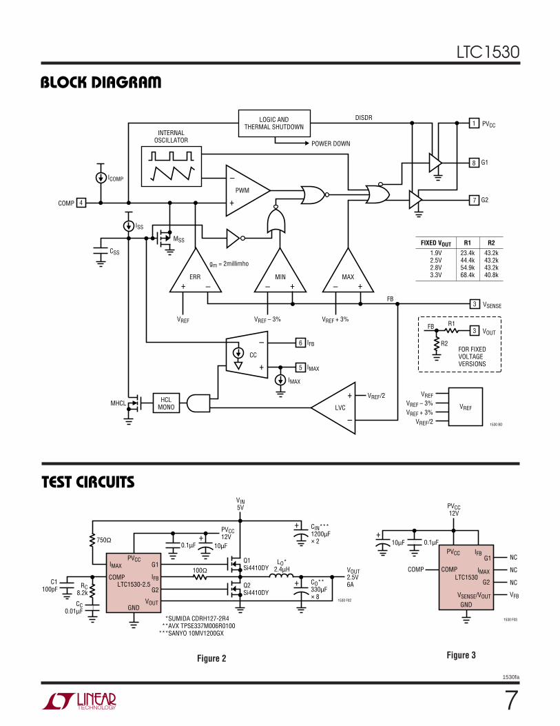
The LTC1530 is a voltage feedback, synchronous switch-ing regulator controller (see Block Diagram) designed foruse in high power, low voltage step-down (buck) convert-ers. It includes an on-chip soft-start capacitor, a PWMgenerator, a precision reference trimmed to ±1%, two highpower MOSFET gate drivers and all the necessary feed-back and control circuitry to form a complete switchingregulator circuit running at 300kHz.
The LTC1530 includes a current limit sensing circuit thatuses the topside external N-channel power MOSFET as acurrent sensing element, eliminating the need for anexternal sense resistor. If the current comparator, CC,detects an overcurrent condition, the duty cycle is reducedby discharging the internal soft-start capacitor through avoltage-controlled current source. Under severe over-loads or output short-circuit conditions, the soft-startcapacitor is pulled to ground and a start-up cycle isinitiated. If the short circuit or overload persists, the chiprepeats soft-start cycles and prevents damage to externalcomponents.
THEORY OF OPERATION
Primary Feedback Loop
The LTC1530 compares the output voltage with the inter-nal reference at the error amplifier inputs. The erroramplifier outputs an error signal to the PWM comparator.This signal is compared to the fixed frequency oscillator
sawtooth waveform to generate the PWM signal. ThePWM signal drives the external MOSFETs at the G1 and G2pins. The resulting chopped waveform is filtered by LO andCOUT which closes the loop. Loop frequency compensa-tion is typically accomplished with an external RC + Cnetwork at the COMP pin, which is the output node of thetransconductance error amplifier.
MIN, MAX Feedback Loops
Two additional comparators in the feedback loop providehigh speed fault correction in situations where the erroramplifier cannot respond quickly enough. MIN comparesthe feedback signal to a voltage 3% below the internalreference. If the signal is below the comparator threshold,the MIN comparator overrides the error amplifier andforces the loop to maximum duty cycle, typically 86%.Similarly, the MAX comparator forces the output to 0%duty cycle if the feedback signal is greater than 3% abovethe internal reference. To prevent these two comparatorsfrom triggering due to noise, the MIN and MAX compara-tors’ response times are deliberately delayed by two tothree microseconds. These comparators help preventextreme output perturbations with fast output load currenttransients, while allowing the main feedback loop to beoptimally compensated for stability.
Thermal Shutdown
The LTC1530 has a thermal protection circuit that disablesboth internal gate drivers if activated. G1 and G2 are heldlow and the LTC1530 supply current drops to about 1mA.
TEST CIRCUITS
APPLICATIO S I FOR ATIO
WU UU
9
LTC1530
1530fa
Typically, thermal shutdown is activated if the LTC1530’sjunction temperature exceeds 150°C. G1 and G2 resumeswitching when the junction temperature drops below100°C.
Soft-Start and Current Limit
Unlike other PWM parts, the LTC1530 includes an on-chipsoft-start capacitor that is used during start-up and cur-rent limit operation. On power-up, an internal 4µA pull-upat COMP brings the LTC1530 out of shutdown mode. Aninternal current source then charges the internal CSScapacitor. The COMP pin is clamped to one VGS above thevoltage on CSS during start-up. This prevents the erroramplifier from forcing the loop to maximum duty cycle.The LTC1530 operates at low duty cycle as the COMP pinvoltage increases above about 2.4V. The slew rate of thesoft-start capacitor is typically 0.4V/ms. As the voltage onCSS continues to increase, MSS eventually turns off and theerror amplifier regulates the output. The MIN comparatoris disabled if soft-start is active to prevent an override ofthe soft-start function.
The LTC1530 includes another feedback loop to controloperation in current limit. Before each falling edge of G1,the current comparator, CC, samples and holds the volt-age drop across external MOSFET Q1 with the LTC1530’sIFB pin. CC compares the voltage at IFB to the voltage at theIMAX pin. As peak current rises, the voltage across theRDS(ON) of Q1 increases. If the voltage at IFB drops belowIMAX, indicating that Q1’s drain current has exceeded themaximum desired level, CC pulls current out of CSS. Dutycycle decreases and the output current is controlled. TheCC comparator pulls current out of CSS in proportion to thevoltage difference between IFB and IMAX. Under minoroverload conditions, the voltage at CSS falls gradually,creating a time delay before current limit activates. Veryshort, mild overloads may not affect the output voltage atall. Significant overload conditions allow the voltage onCSS to reach a steady state and the output remains at areduced voltage until the overload is removed. Seriousoverloads generate a large overdrive and allow CC to pullthe CSS voltage down quickly, thus preventing damage tothe external components.
By using the RDS(ON) of Q1 to measure output current, thecurrent limit circuit eliminates the sense resistor thatwould otherwise be required. This minimizes the numberof components in the high current power path. The currentlimit circuitry is not designed to be highly accurate. It isprimarily meant to prevent damage to the power supplycircuitry during fault conditions. The exact current levelwhere current limiting takes effect will vary from unit tounit as the RDS(ON) of Q1 varies.
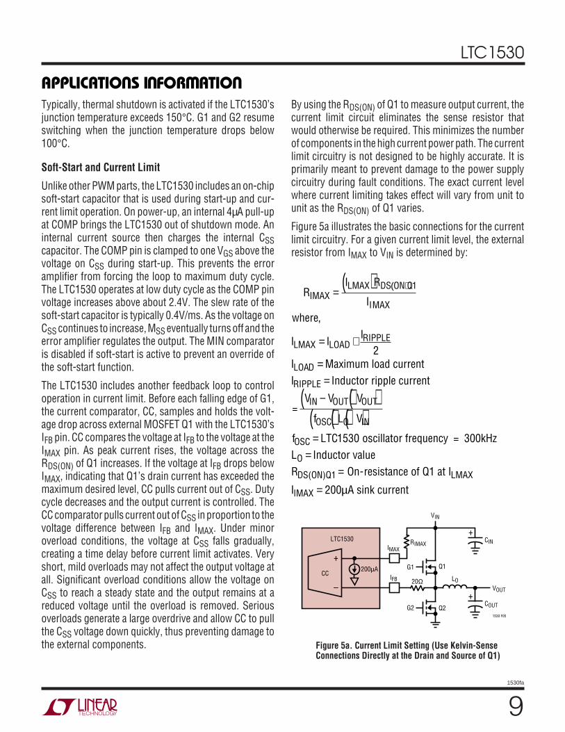
Figure 5a illustrates the basic connections for the currentlimit circuitry. For a given current limit level, the externalresistor from IMAX to VIN is determined by:
LTC1530
+
+CIN
COUT
VOUT
1530 F05
VIN
LO20ΩIFB
G1 Q1
Q2G2
IMAXRIMAX
200µA
+
–
CC
Maximum load currentI Inductor ripple current
=V
f
oscillator frequency = 300kHzL valueR n-r tance of Q1 at I
200 A sink current
RIPPLE
IN
OSC
O
DS(ON)Q1 LMAX
RI R
Iwhere
I II
I
V V
L V
f LTCInductor
O esis
I
IMAXLMAX DS ON Q
IMAX
LMAX LOADRIPPLE
LOAD
OUT OUT
O IN
OSC
IMAX
=( )
= +
==
−( )( )( )( )( )=
==
= µ
( )
,
1
2
1530
Figure 5a. Current Limit Setting (Use Kelvin-SenseConnections Directly at the Drain and Source of Q1)
APPLICATIO S I FOR ATIO
WU UU
10
LTC1530
1530fa
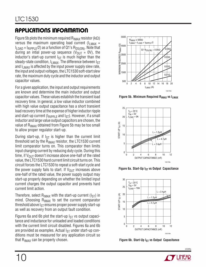
Figure 5b plots the minimum required RIMAX resistor (kΩ)versus the maximum operating load current (ILMAX =ILOAD + IRIPPLE/2) as a function of Q1’s RDS(ON). Note thatduring an intial power-up sequence (VOUT = 0V), theinductor’s start-up current IST is much higher than thesteady-state condition, ILMAX. The difference between ISTand ILMAX is affected by the input power supply slew rate,the input and output voltages, the LTC1530 soft-start slewrate, the maximum duty cycle and the inductor and outputcapacitor values.
For a given application, the input and output requirementsare known and determine the main inductor and outputcapacitor values. These values establish the transient loadrecovery time. In general, a low value inductor combinedwith high value output capacitance has a short transientload recovery time at the expense of higher inductor rippleand start-up current (IRIPPLE and IST). However, if a smallinductor and large value output capacitors are chosen, thevalue of RIMAX obtained from Figure 5b may be too smallto allow proper regulator start-up.
During start-up, if IST is higher than the current limitthreshold set by the RIMAX resistor, the LTC1530 currentlimit comparator turns on. This comparator then limitsinput charging current by reducing duty cycle. During thistime, if VOUT doesn’t increase above one-half of the ratedvalue, the LTC1530 hard current limit circuit turns on. Thiscircuit forces the LTC1530 to repeat a soft-start cycle andthe power supply fails to start. If VOUT increases aboveone-half of the rated value, the power supply output maystart-up properly depending on whether the limited inputcurrent charges the output capacitor and prevents hardcurrent limit action.
Therefore, select RIMAX with the start-up current (IST) inmind. Choosing RIMAX to set the current comparatorthreshold above IST ensures proper power supply start-upas well as recovery from an output fault condition.
Figures 6a and 6b plot the start-up IST vs output capaci-tance and inductance for unloaded and loaded conditionswith the current limit circuit disabled. Figures 6a and 6bare provided as examples. Actual IST under start-up con-ditions must be measured for any application circuit sothat RIMAX can be properly chosen.
ILMAX (A)0
MIN
IMUM
REQ
UIRE
D R I
MAX
(Ω)
5500
4500
3500
2500
1500
50016 18
1530 F05b
42 6 8 10 1412 20
RIMAX ≥ 500ΩILMAX = ILOAD + IRIPPLE/2
Q1 RDS(ON) = 0.05Ω 0.04Ω
0.03Ω
0.02Ω
0.01Ω
Figure 5b. Minimum Required RIMAX vs ILMAX
OUTPUT CAPACITANCE (mF)0
STAR
T-UP
I ST
(A)
25
20
15
10
5
02 4 6 8
1530 F06a
10 12
TA = 25°CVIN = 5VILOAD = 0A
L = 1.2µH
L = 4.7µH
L = 2.4µH
Figure 6a. Start-Up IST vs Output Capacitance
OUTPUT CAPACITANCE (mF)0
STAR
T-UP
I ST
(A)
30
25
20
15
10
5
02 4 6 8
1530 F06b
10 12
TA = 25°CVIN = 5VILOAD = 10A
L = 1.2µH
L = 4.7µH
L = 2.4µH
Figure 6b. Start-Up IST vs Output Capacitance
APPLICATIO S I FOR ATIO
WU UU

11
LTC1530
1530fa
Power MOSFETs
Two N-channel power MOSFETs are required for synchro-nous LTC1530 circuits. They should be selected basedprimarily on threshold voltage and on-resistance consid-erations. Thermal dissipation is often a secondary con-cern in high efficiency designs. The required MOSFETthreshold should be determined based on the availablepower supply voltages and/or the complexity of the gatedrive charge pump scheme. In 5V input designs where a12V supply is used to power PVCC, standard MOSFETswith RDS(ON) specified at VGS = 5V or 6V can be used withgood results. The current drawn from the 12V supplyvaries with the MOSFETs used and the LTC1530’s operat-ing frequency, but is generally less than 50mA.
LTC1530 applications that use a 5V VIN voltage and adoubling charge pump to generate PVCC do not provideenough gate drive voltage to fully enhance standardpower MOSFETs. Under this condition, the effectiveMOSFET RDS(ON) may be quite high, raising the dissipa-tion in the FETs and reducing efficiency. In addition,power supply start-up problems can occur with standardpower MOSFETs. These start-up problems can occur fortwo reasons. First, if the MOSFET is not fully enhanced,the higher effective RDS(ON) causes the LTC1530 to acti-vate current limit at a much lower level than the desiredtrip point. Second, standard MOSFETs have higher GATEthreshold voltages than logic level MOSFETs, therebyincreasing the PVCC voltage required to turn them on. AMOSFET whose RDS(ON) is rated at VGS = 4.5V does notnecessarily have a logic level MOSFET GATE thresholdvoltage. Logic level FETs are the recommended choice for5V-only systems. Logic level FETs can be fully enhancedwith a doubler charge pump and will operate at maximumefficiency. Note that doubler charge pump designs run-ning from supplies higher than 6.5V should include aZener diode clamp at PVCC to prevent transients fromexceeding the absolute maximum rating of the pin.
After the MOSFET threshold voltage is selected, choosethe RDS(ON) based on the input voltage, the output voltage,allowable power dissipation and maximum output cur-rent. In a typical LTC1530 buck converter circuit, operat-ing in continuous mode, the average inductor current isequal to the output load current. This current flows through
+ +
0.22µF
10µF
+CO
CIN
LO
MBR0530T1 MBR0530T1OPTIONAL FORVIN > 6.5V
LTC1530
PVCC
G1
VOUT
1530 F07
VIN
13V1N5243B
Q1
Q2G2
In order for the current limit circuit to operate properly andto obtain a reasonably accurate current limit threshold, theIMAX and IFB pins must be Kelvin sensed at Q1’s drain andsource pins. A 0.1µF decoupling capacitor can also beconnected across RIMAX to filter switching noise. In addi-tion, LTC recommends that the voltage drop across theRIMAX resistor be set to ≥100mV. Otherwise, noise spikesor ringing at Q1’s source can cause the actual current limitto be greater than the desired current limit set point.
MOSFET Gate Drive
The PVCC supply must be greater than the input supplyvoltage, VIN, by at least one power MOSFET VGS(ON) forefficient operation. This higher voltage can be suppliedwith a separate supply, or it can be generated using asimple charge pump as shown in Figure 7. The 86%maximum duty cycle ensures sufficient off-time to refreshthe charge pump during each cycle.
As PVCC is powered up from 0V, the LTC1530 undervolt-age lockout circuit prevents G1 and G2 from pulling highuntil PVCC reaches about 3.5V. To prevent Q1’s highRDS(ON) from triggering the current limit comparator whilePVCC is slewing, the current limit circuit is disabled untilPVCC is≥8V. In addition, on start-up or recovery fromthermal shutdown, the driver logic is designed to hold G2low until G1 first goes high.
Figure 7. Doubling Charge Pump
APPLICATIO S I FOR ATIO
WU UU
12
LTC1530
1530fa
Note that while the required RDS(ON) values suggest largeMOSFETs, the power dissipation numbers are only 1.39Wper device or less—large TO-220 packages and heatsinks are not necessarily required in high efficiency appli-cations. Siliconix Si4410DY or International RectifierIRF7413 (both in SO-8) or Siliconix SUD50N03 or MotorolaMTD20N03HDL (both in DPAK) are small footprint sur-face mount devices with RDS(ON) values below 0.03Ω at 5Vof VGS that work well in LTC1530 circuits. With higheroutput voltages, the RDS(ON) of Q1 may need to be signifi-cantly lower than that for Q2. These conditions can oftenbe met by paralleling two MOSFETs for Q1 and using asingle device for Q2. Using a higher PMAX value in theRDS(ON) calculations generally decreases the MOSFETcost and the circuit efficiency and increases the MOSFETheat sink requirements.
In most LTC1530 applications, RDS(ON) is used as thecurrent sensing element. MOSFET RDS(ON) has a positivetemperature coefficient. Therefore, the LTC1530 IMAX sinkcurrent is designed with a positive 3300ppm/°C tempera-ture coefficient. The positive tempco of IMAX provides firstorder correction for current limit vs temperature. There-fore, current limit does not have to be set to an increasedlevel at room temperature to guarantee a desired outputcurrent at elevated temperatures.
Table 1 highlights a variety of power MOSFETs that aresuitable for use in LTC1530 applications.
Inductor Selection
The inductor is often the largest component in an LTC1530design and must be chosen carefully. Choose the inductorvalue and type based on output slew rate requirementsand expected peak current. The required output slew rateprimarily controls the inductor value. The maximum rateof rise of inductor current is set by the inductor’s value, theinput-to-output voltage differential and the LTC1530’smaximum duty cycle. In a typical 5V input, 2.8V outputapplication, the maximum rise time will be:
DCV V
L LMAXIN OUT−
= 1 85.
Asµ
either Q1 or Q2 with the power dissipation split up accord-ing to the duty cycle:
DC QVV
DC QVV
V V
V
OUT
IN
OUT
IN
IN OUT
IN
( )
( )
1
2 1
=
= − =−( )
The RDS(ON) required for a given conduction loss can nowbe calculated by rearranging the relation P = I2R.
RP
DC Q I
V P
V I
RP
DC Q I
V P
V V I
DS ON QMAX Q
MAX
IN MAX Q
OUT MAX
DS ON QMAX Q
MAX
IN MAX Q
IN OUT MAX
( )( )
( )
( )( )
( )
( )
( )
11
2
12
22
2
22
1
2
=[ ]( )
=( )[ ]( )( )
=[ ]( )
=( )[ ]
−( )( )
PMAX should be calculated based primarily on requiredefficiency or allowable thermal dissipation. A high efficiencybuck converter designed for the Pentium II with 5V inputand a 2.8V, 11.2A output might allow no more than 4%efficiency loss at full load for each MOSFET. Assumingroughly 90% efficiency at this current level, this gives a PMAXvalue of:
(2.8)(11.2A/0.9)(0.04) = 1.39W per FET
and a required RDS(ON) of:
RV W
V A
RV W
V V A
DS ON Q
DS ON Q
( )
( )
.
. ..
.
. ..
1 2
2 2
5 1 39
2 8 11 20 020
5 1 39
5 2 8 11 20 025
=( )
=
=( )
−( )
=
Ω
Ω
APPLICATIO S I FOR ATIO
WU UU

13
LTC1530
1530fa
where L is the inductor value in µH. With proper frequencycompensation, the combination of the inductor and outputcapacitor values determine the transient recovery time. Ingeneral, a smaller value inductor improves transientresponse at the expense of ripple and inductor coresaturation rating. A 2µH inductor has a 0.9A/µs rise timein this application, resulting in a 5.5µs delay in respondingto a 5A load current step. During this 5.5µs, the differencebetween the inductor current and the output current ismade up by the output capacitor. This action causes atemporary voltage droop at the output. To minimize thiseffect, the inductor value should usually be in the 1µH to5µH range for most 5V input LTC1530 circuits. Differentcombinations of input and output voltages and expectedloads may require different values.
Once the required inductor value is selected, choose theinductor core type based on peak current and efficiencyrequirements. Peak current in the inductor is equal to themaximum output load current plus half of the peak-to-peak inductor ripple current. Inductor ripple current is setby the inductor’s value, the input voltage, the outputvoltage and the operating frequency. If the efficiency ishigh, ripple current is approximately equal to:
IV V V
f L VRIPPLE
IN OUT OUT
OSC O IN=
−( )( )( )( )( )
wherefOSC = LTC1530 oscillator frequencyLO = Inductor value
Solving this equation for a typical 5V to 2.8V applicationwith a 2µH inductor, ripple current is:
2 2 0 56
300 22
. .V
kHz HA
( )( )( )( ) =
µP-P
Peak inductor current at 11.2A load:
11 222
12 2. .AA
A+ =
The ripple current should generally fall between 10% and40% of the output current. The inductor must be able towithstand this peak current without saturating, and thecopper resistance in the winding should be kept as low aspossible to minimize resistive power loss. Note that in
APPLICATIO S I FOR ATIO
WU UU
RDS(ON) TYPICAL INPUTAT 25°C RATED CURRENT CAPACITANCE θθθθθJC TJMAX
MANUFACTURER PART NO. PACKAGE (Ω) (A) Ciss (pF) (°C/W) (°C)
Siliconix SUD50N03-10 TO-252 0.019 15A at 25°C 3200 1.8 17510A at 100°C
Siliconix Si4410DY SO-8 0.020 10A at 25°C 2700 — 1508A at 75°C
ON Semiconductor MTD20N03HDL DPAK 0.035 20A at 25°C 880 1.67 15016A at 100°C
Fairchild FDS6680 SO-8 0.01 11.5A at 25°C 2070 25 150
ON Semiconductor MTB75N03HDL* D2PAK 0.0075 75A at 25°C 4025 1.0 15059A at 100°C
IR IRL3103S D2PAK 0.014 56A at 25°C 1600 1.8 17540A at 100°C
IR IRLZ44 TO-220 0.028 50A at 25°C 3300 1.0 17536A at 100°C
Fuji 2SK1388 TO-220 0.037 35A at 25°C 1750 2.08 150
Note: Please refer to the manufacturer’s data sheet for testing conditions and detailed information.*Users must consider the power dissipation and thermal effects in the LTC1530 if driving external MOSFETs with high values of input capacitance.Refer to the PVCC Supply Current vs GATE Capacitance in the Typical Performance Characteristics section.
Table 1. Recommended MOSFETs for LTC1530 Applications
14
LTC1530
1530fa
circuits not employing the current limit function, thecurrent in the inductor may rise above this maximumunder short circuit or fault conditions; the inductor shouldbe sized accordingly to withstand this additional current.Inductors with gradual saturation characteristics (example:powdered iron) are often the best choice.
Input and Output Capacitors
A typical LTC1530 design places significant demands onboth the input and the output capacitors. During normalsteady load operation, a buck converter like the LTC1530draws square waves of current from the input supply at theswitching frequency. The peak current value is equal to theoutput load current plus 1/2 the peak-to-peak ripple cur-rent. Most of this current is supplied by the input bypasscapacitor. The resulting RMS current flow in the inputcapacitor heats it and causes premature capacitor failurein extreme cases. Maximum RMS current occurs with50% PWM duty cycle, giving an RMS current value equalto IOUT/2. A low ESR input capacitor with an adequateripple current rating must be used to ensure reliableoperation. Note that capacitor manufacturers’ ripple cur-rent ratings are often based on only 2000 hours (3 months)lifetime at rated temperature. Further derating of the inputcapacitor ripple current beyond the manufacturer’s speci-fication is recommended to extend the useful life of thecircuit. Lower operating temperature has the largest effecton capacitor longevity.
The output capacitor in a buck converter under steadystate conditions sees much less ripple current than theinput capacitor. Peak-to-peak current is equal to inductorripple current, usually 10% to 40% of the total loadcurrent. Output capacitor duty places a premium not onpower dissipation but on ESR. During an output loadtransient, the output capacitor must supply all of theadditional load current demanded by the load until theLTC1530 adjusts the inductor current to the new value.ESR in the output capacitor results in a step in the outputvoltage equal to the ESR value multiplied by the change inload current. An 11A load step with a 0.05Ω ESR outputcapacitor results in a 550mV output voltage shift; this is19.6% of the output voltage for a 2.8V supply! Because ofthe strong relationship between output capacitor ESR and
output load transient response, choose the output capaci-tor for ESR, not for capacitance value. A capacitor withsuitable ESR will usually have a larger capacitance valuethan is needed to control steady-state output ripple.
Electrolytic capacitors rated for use in switching powersupplies with specified ripple current ratings and ESR canbe used effectively in LTC1530 applications. OS-CONelectrolytic capacitors from Sanyo and other manufactur-ers give excellent performance and have a very highperformance/size ratio for electrolytic capacitors. Surfacemount applications can use either electrolytic or drytantalum capacitors. Tantalum capacitors must be surgetested and specified for use in switching power supplies.Low cost, generic tantalums are known to have very shortlives followed by explosive deaths in switching powersupply applications. AVX TPS series surface mountdevices are popular surge tested tantalum capacitors thatwork well in LTC1530 applications.
A common way to lower ESR and raise ripple currentcapability is to parallel several capacitors. A typicalLTC1530 application might exhibit 5A input ripple cur-rent. Sanyo OS-CON capacitors, part number 10SA220M(220µF/10V), feature 2.3A allowable ripple current at85°C; three in parallel at the input (to withstand the inputripple current) meet the above requirements. Similarly,AVX TPSE337M006R0100 (330µF/6V) capacitors have arated maximum ESR of 0.1Ω; seven in parallel lower thenet output capacitor ESR to 0.014Ω. For low costapplications, the Sanyo MV-GX capacitor series can beused with acceptable performance.
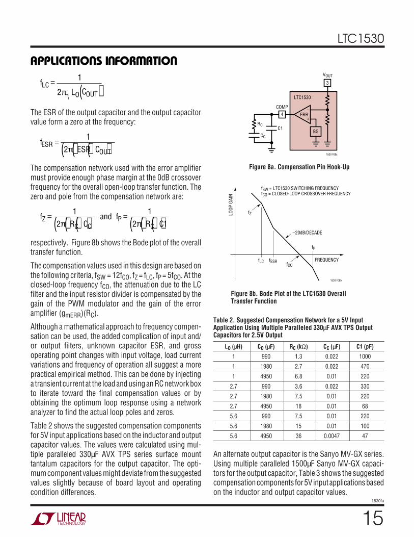
Feedback Loop Compensation
The LTC1530 voltage feedback loop is compensated at theCOMP pin, which is the output node of the gm erroramplifier. The feedback loop is generally compensatedwith an RC + C network from COMP to GND as shown inFigure 8a.
Loop stability is affected by the values of the inductor, theoutput capacitor, the output capacitor ESR, the erroramplifier transconductance and the error amplifier com-pensation network. The inductor and the output capacitorcreate a double pole at the frequency:
APPLICATIO S I FOR ATIO
WU UU
15
LTC1530
1530fa
fL C
LCO OUT
=( )1
2π
The ESR of the output capacitor and the output capacitorvalue form a zero at the frequency:
fESR C
ESROUT
= ( )( )( )1
2π
The compensation network used with the error amplifiermust provide enough phase margin at the 0dB crossoverfrequency for the overall open-loop transfer function. Thezero and pole from the compensation network are:
fR C
and fR C
ZC C
PC
= ( )( )( ) = ( )( )( )1
21
2 1π π
respectively. Figure 8b shows the Bode plot of the overalltransfer function.
The compensation values used in this design are based onthe following criteria, fSW = 12fCO, fZ = fLC, fP = 5fCO. At theclosed-loop frequency fCO, the attenuation due to the LCfilter and the input resistor divider is compensated by thegain of the PWM modulator and the gain of the erroramplifier (gmERR)(RC).
Although a mathematical approach to frequency compen-sation can be used, the added complication of input and/or output filters, unknown capacitor ESR, and grossoperating point changes with input voltage, load currentvariations and frequency of operation all suggest a morepractical empirical method. This can be done by injectinga transient current at the load and using an RC network boxto iterate toward the final compensation values or byobtaining the optimum loop response using a networkanalyzer to find the actual loop poles and zeros.
Table 2 shows the suggested compensation componentsfor 5V input applications based on the inductor and outputcapacitor values. The values were calculated using mul-tiple paralleled 330µF AVX TPS series surface mounttantalum capacitors for the output capacitor. The opti-mum component values might deviate from the suggestedvalues slightly because of board layout and operatingcondition differences.
APPLICATIO S I FOR ATIO
WU UU
C1RC
CC
LTC1530
VOUT
COMP
1530 F08a
+
–ERR
BG
3
4
Figure 8a. Compensation Pin Hook-Up
LOOP
GAI
N
FREQUENCY
1530 F08b
–20dB/DECADE
fSW = LTC1530 SWITCHING FREQUENCYfCO = CLOSED-LOOP CROSSOVER FREQUENCY
fZ
fLC fESR fCO
fP
Figure 8b. Bode Plot of the LTC1530 OverallTransfer Function
Table 2. Suggested Compensation Network for a 5V InputApplication Using Multiple Paralleled 330µF AVX TPS OutputCapacitors for 2.5V Output
LO (µH) CO (µF) RC (kΩ) CC (µF) C1 (pF)
1 990 1.3 0.022 1000
1 1980 2.7 0.022 470
1 4950 6.8 0.01 220
2.7 990 3.6 0.022 330
2.7 1980 7.5 0.01 220
2.7 4950 18 0.01 68
5.6 990 7.5 0.01 220
5.6 1980 15 0.01 100
5.6 4950 36 0.0047 47
An alternate output capacitor is the Sanyo MV-GX series.Using multiple paralleled 1500µF Sanyo MV-GX capaci-tors for the output capacitor, Table 3 shows the suggestedcompensation components for 5V input applications basedon the inductor and output capacitor values.
16
LTC1530
1530fa
Table 3. Suggested Compensation Network for a 5V InputApplication Using Multiple Paralleled 1500µF SANYO MV-GXOutput Capacitors for 2.5V Output
LO (µH) CO (µF) RC (kΩ) CC (µF) C1 (pF)
1 4500 3 0.022 470
1 6000 4 0.022 330
1 9000 6 0.022 220
2.7 4500 8.2 0.022 150
2.7 6000 11 0.01 100
2.7 9000 16 0.01 100
5.6 4500 16 0.01 100
5.6 6000 22 0.01 68
5.6 9000 33 0.01 47
Note: For different values of VOUT, multiply the RC value by VOUT/2.5 andmultiply the CC and C1 values by 2.5/VOUT. This maintains the samecrossover frequency for the closed-loop transfer function.
Thermal Considerations
Limit the LTC1530’s junction temperature to less than125°C. The LTC1530’s SO-8 package is rated at 130°C/Wand care must be taken to ensure that the worst-case inputvoltage and gate drive load current requirements do notcause excessive die temperatures. Short-circuit or faultconditions may activate the internal thermal shutdowncircuit.
LAYOUT CONSIDERATIONS
When laying out the printed circuit board (PCB), thefollowing checklist should be used to ensure properoperation of the LTC1530. These items are illustratedgraphically in the layout diagram of Figure 9. The thickerlines show the high current power paths. Note that at 10Acurrent levels or above, current density in the PCB itself isa serious concern. Traces carrying high current should beas wide as possible. For example, a PCB fabricated with2oz copper requires a minimum trace width of 0.15" tocarry 10A, and only if trace length is kept short.
1. In general, begin the layout with the location of thepower devices. Orient the power circuitry so that aclean power flow path is achieved. Maximize conduc-tor widths but minimize conductor lengths. Keep highcurrent connections on one side of the PCB if possible.If not, minimize the use of vias and keep the currentdensity in the vias to <1A/via, preferably < 0.5A/via.
After achieving a satisfactory power path layout, pro-ceed with the control circuitry layout. It is much easierto find routes for the relatively small traces in thecontrol circuits than it is to find circuitous routes forhigh current paths.
2. Tie the GND pin to the ground plane at a single point,preferably at a fairly quiet point in the circuit, such as thebottom of the output capacitors. However, this is notalways practical due to physical constraints. Connectthe low side source to the input capacitor ground.Connect the input and output capacitor to the groundplane. Run a separate trace for the low side FET sourceto the input capacitors. Do not tie this single pointground in the trace run between the low side FET sourceand the input capacitor ground. This area of the groundplane is very noisy.
3. Locate the small signal resistor and capacitors used forfrequency compensation close to the COMP pin. Use aseparate ground trace for these components that tiesdirectly to the GND pin of the LTC1530. Do not connectthese components to the ground plane!
4. Place the PVCC decoupling capacitor as close to theLTC1530 as possible. The 10µF bypass capacitor shownat PVCC helps provide optimum regulation performanceby minimizing ripple at the PVCC pin.
5. Connect the (+) plate of CIN as close as possible to thedrain of the upper MOSFET. LTC recommends anadditional 1µF low ESR ceramic capacitor between VINand power ground.
6. The VSENSE/VOUT pin is very sensitive to pickup from theswitching node. Care must be taken to isolate this pinfrom capacitive coupling to the high current inductorswitching signals. A 0.1µF is recommended betweenthe VOUT pin and the GND pin directly at the LTC1530 forfixed voltage versions. For the adjustable voltage ver-sion, keep the resistor divider close to the LTC1530.The bottom resistor’s ground connection should tiedirectly to the LTC1530’s GND pin.
7. Kelvin sense IMAX and IFB at the drain and source pinsof Q1.
8. Minimize the length of the gate lead connections.
APPLICATIO S I FOR ATIO
WU UU

17
LTC1530
1530fa
+10µF
LO
PVCC
PVCC
GND
G1
G2
COMP
LTC1530
IFB
IMAX
1
2
3
4
8
7
6
5VOUT VOUT
1530 F09
VIN
RC
RIFB
RIMAX
CC
CIN0.1µF
0.1µF
Q1
Q2
C1
BOLD LINES INDICATEHIGH CURRENT PATHS
COUT+
+
Figure 9. LTC1530 Layout Diagram
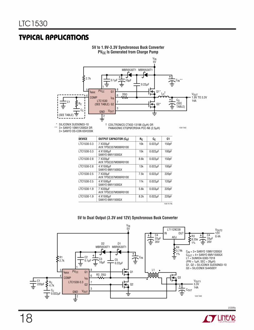
DEVICE OUTPUT CAPACITOR (CO) RC CC C1
LTC1530-3.3 7 X330µF 10k 0.022µF 150pFAVX TPSE337M006R0100
LTC1530-3.3 4 X1500µF 15k 0.022µF 100pFSANYO 6MV1500GX
LTC1530-2.8 7 X330µF 8.6k 0.022µF 150pFAVX TPSE337M006R0100
LTC1530-2.8 4 X1500µF 13k 0.022µF 100pFSANYO 6MV1500GX
LTC1530-2.5 7 X330µF 7.5k 0.022µF 220pFAVX TPSE337M006R0100
LTC1530-2.5 4 X1500µF 11k 0.022µF 120pFSANYO 6MV1500GX
LTC1530-1.9 7 X330µF 5.6k 0.033µF 220pFAVX TPSE337M006R0100
LTC1530-1.9 4 X1500µF 8.2k 0.022µF 220pFSANYO 6MV1500GX
1530 TA TBL
Figure 10. 5V to 1.9V-3.3V Synchronous Buck ConverterPVCC Is Powered from 12V Supply
+ +0.1µF10µF
+ CO(SEETABLE)
CIN**
LO†
20Ω
2.7kPVCC12V
PVCC
GND
LTC1530(SEE TABLE)
G1
1 5
2
4
8
6
7
3
COMP IFB
IMAX
G2
VOUT
VOUT1.9V TO 3.3V14A
1530 F10
VIN5V
* SILICONIX SUD50N03-10** 3× SANYO 10MV1200GX OR
3× SANYO OS-CON 6SH330K
RC
CC
Q1*
Q2*C1
† COILTRONICS CTX02-13198 (2µH) OR PANASONIC ETQP6F2R5HA PCC-N6 (2.5µH)
(SEE TABLE)
APPLICATIO S I FOR ATIO
WU UU
18
LTC1530
1530fa
5V to 1.9V-3.3V Synchronous Buck ConverterPVCC Is Generated from Charge Pump
+ +0.1µF
0.22µF10µF
+ CO(SEETABLE)
CIN**
LO†
20Ω
2.7k
PVCC
GND
LTC1530(SEE TABLE)
G1
15
2
4
8
6
7
3
COMP IFB
IMAX
G2
VOUT
1530 TA02
VIN5V
* SILICONIX SUD50N03-10** 3× SANYO 10MV1200GX OR
3× SANYO OS-CON 6SH330K
RC
CC
Q1*
Q2*C1
† COILTRONICS CTX02-13198 (2µH) ORPANASONIC ETQP6F2R5HA PCC-N6 (2.5µH)
(SEE TABLE)
VOUT1.9V TO 3.3V14A
MBR0530T1 MBR0530T1
DEVICE OUTPUT CAPACITOR (CO) RC CC C1
LTC1530-3.3 7 X330µF 10k 0.022µF 150pFAVX TPSE337M006R0100
LTC1530-3.3 4 X1500µF 15k 0.022µF 100pFSANYO 6MV1500GX
LTC1530-2.8 7 X330µF 8.6k 0.022µF 150pFAVX TPSE337M006R0100
LTC1530-2.8 4 X1500µF 13k 0.022µF 100pFSANYO 6MV1500GX
LTC1530-2.5 7 X330µF 7.5k 0.022µF 220pFAVX TPSE337M006R0100
LTC1530-2.5 4 X1500µF 11k 0.022µF 120pFSANYO 6MV1500GX
LTC1530-1.9 7 X330µF 5.6k 0.033µF 220pFAVX TPSE337M006R0100
LTC1530-1.9 4 X1500µF 8.2k 0.022µF 220pFSANYO 6MV1500GX
1530 TA TBL
+ +C20.1µF C5
0.22µFC310µF
+
+
CIN
L1
R2, 20Ω
R12.7k
PVCC
GND
LTC1530-3.3
G1
15
2
4
8
6
7
3
COMP IFB
IMAX
G2
VOUT
1530 TA09
VIN5V
CIN = 3× SANYO 10MV1200GXCOUT = 4× SANYO 6MV1500GXL1 = SUMIDA 6383-T018(PRI = 1µH, SEC = 26µH)Q1, Q2 = SILICONIX SUD50N03-10Q3 = SILICONIX Si4450DY
RC4.7k
CC0.022µF
Q1
Q2
Q3
R43.74k1%
C422µF35V
+ C433µF20V
C1220pF
VOUT13.3V14A
VOUT212V0.4A
COUT
D2MBR0530T1
D1MBR0530T1
IN OUTADJ
LT1129CS8
R38.25k1%
5V to Dual Output (3.3V and 12V) Synchronous Buck Converter
TYPICAL APPLICATIO S
U
19
LTC1530
1530fa
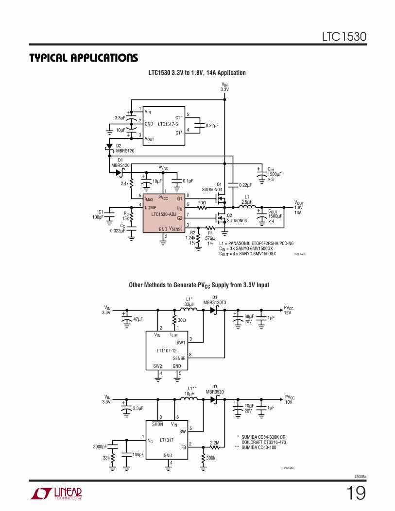
LTC1530 3.3V to 1.8V, 14A Application
+
+
+
+
0.1µF0.22µF
0.22µF
10µF
10µF
3.3µF
+ COUT1500µF× 4
CIN1500µF× 3
L12.5µH20Ω
R1576Ω1%
R21.24k
1%
2.4k
PVCC
PVCC
GND
LTC1530-ADJ
LTC1517-5
G1
15
3
2
C1+
C1–
4
51
2
4
8
6
7
3
COMP IFB
IMAX
G2
VSENSE
VOUT
GND
VIN
1530 TA03
VIN3.3V
L1 = PANASONIC ETQP6F2R5HA PCC-N6CIN = 3× SANYO 6MV1500GXCOUT = 4× SANYO 6MV1500GX
RC13k
CC0.022µF
Q2SUD50N03
Q1SUD50N03
C1100pF
VOUT1.8V14A
D1MBRS120
D2MBRS120
Other Methods to Generate PVCC Supply from 3.3V Input
1µF
PVCC12V+
68µF20V
+47µF
L1*33µH
30Ω
VIN
GNDSW2
LT1107-12
2 1
4 5
8
3SW1
ILIM
SENSE
1530 TA04
VIN3.3V
* SUMIDA CD54-330K ORCOILCRAFT DT3316-473
** SUMIDA CD43-100
D1MBRS120T3
1µF
PVCC10V+ 10µF
20V
+3.3µF
100pF
3000pF
L1**10µH
SHDN VIN
GND
VC LT1317
3 6
1
4
2
5SW
FB
VIN3.3V
D1MBR0520
33k 300k
2.2M
TYPICAL APPLICATIO S
U

20
LTC1530
1530fa
LTC1530 High Efficiency Boost Converter
PVCC
GND
LTC1530G1
1 5
2
1530 TA05a
4
8
7
6
Q3IRF7811
Q4IRF7811
R771.5k1%
R623.2k1%
Q2IRF7811
D2MBR0530T1
R4360Ω D3
MBRS140T3
3
COMP G2
IMAX IFB
VSENSE
R247k
D1FMMD914
+C16330µF
10VC17330µF10V
C18330µF
10V
L11µH
+C14330µF
10V+ C15
330µF10V
C131µF16V
VOUT5V6A
+
L22.1µH
R50.005Ω
5%
+C12470µF6V
C90.22µF
16V
+
C110µF16VC8
1µF16V
C61µF16V
+
C11470µF
6V
+
C101µF16V
C21µF16V
C31µF16V
R110k
R347k
C50.022µF
Q1FMMT3904
L1 = COILCRAFT DO3316P-102L2 = SUMIDA CEE125C-2R1
VIN
GND
VOUT
C1–
C1+
C4100pF
C70.22µF16V
51
VIN3.3V
2
3
4LTC1517-5
Efficiency vs Load Current
LOAD CURRENT (A)0
0
EFFI
CIEN
CY (%
)
20
40
60
1 2 3 4
1530 TA05b
5
80
100
10
30
50
70
90
6
TA = 25°CVIN = 3.3VVOUT = 5V
TYPICAL APPLICATIO S
U
21
LTC1530
1530fa
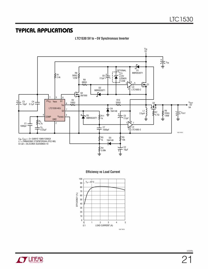
Efficiency vs Load Current
LOAD CURRENT (A)00.1
EFFI
CIEN
CY (%
)
1 2 3 4
1530 TA07b
5
100
90
80
70
60
50
40
30
20
10
0
TA = 25°C
LTC1530 5V to –5V Synchronous Inverter
CIN
6 5
4
3
PVCC
GND
LTC1530-ADJG2
1 5
2
4
7
6
8
3COMP
IFB
IMAX G1
VSENSE
CIN, COUT = 3× SANYO 10MV1200GXL1 = PANASONIC ETQP6F2R5HA (PCC-N6)Q1,Q2 = SILICONIX SUD50N03-10
RC4.7k
R2100Ω
R12.4k
R8560Ω1/2W
CC0.22µF
C40.1µF
C310µF
C11000pF
R9680Ω
D2MBR0530T1
D31N4148
D1MBR0530T1
OPTIONALZ112VZENER1/2W
+
+
+
C52.2µF
COUT
VOUT–5V5A
L12.5µH
C210µF
R510k
R31k
R43.09k
1530 TA07a
Q32N7000
1/2LTC1693-2
1/2LTC1693-2
VIN5V
C71000pF
R10330Ω
D5MBR0530T1
D41N4148
Q2
Q1
C62.2µF
+
+
R111k
R74.7Ω
R6220Ω1/6W
1 8 7
2
+
TYPICAL APPLICATIO S
U
22
LTC1530
1530fa
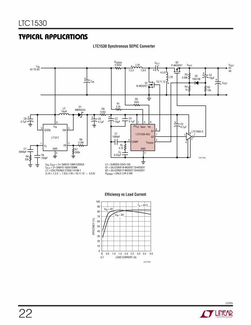
LTC1530 Synchronous SEPIC Converter
LOAD CURRENT (A)00.1
EFFI
CIEN
CY (%
)
0.5 1.0 1.5 2.0 2.5 3.0 3.5
1530 TA08b
4.0
100
90
80
70
60
50
40
30
20
10
0
TA = 25°C
VIN = 8V
VIN = 4V
Efficiency vs Load Current
GNDFB
1
4
5
5
2
4
66
7
8
3
2
3
1
SHDN SWVIN
VC
R833k
R7300k
R62.2M
CC0.22µF
C11000pF
C6100pF
C94.7µF
D1MBR0520
Q1N-MOSFET
D21N4148
Q2P-MOSFET
L1B
•
• L1A
L210µH
VOUT5V4A
VOUT
COUT
C210µF
1530 TA08a
R95.6Ω
C84.7µF
C73000pF
+
+
+
C40.1µF
C310µF
+
+
+
+
C54.7µF
+
RC4.7k
R12.2k
R520Ω
RSENSE0.02ΩVIN
4V TO 8V
CIN
CFLY
IFBPVCC IMAX
LTC1530-ADJLT1317
VSENSE
R33.09k
R41k
R210k
GND
G1
G2
4
8 7
3
1LTC1693-3
CIN, COUT = 3× SANYO 10MV1200GXCFLY = 2× SANYO 16SA150MKL1 = COILTRONIX CTX02-13198-1(L1A = 1,2,3 → 7,8,9; L1B = 10,11,12 → 4,5,6)
L2 = SUMIDA CD43-100 Q1 = SILICONIX N-MOSFET SI4420DYQ2 = SILICONIX P-MOSFET SI4425DYRSENSE = DALE LVR-3 3W
COMP
1,2,34,5,6
10,11,12
7,8,9
TYPICAL APPLICATIO S
U
23
LTC1530
1530fa
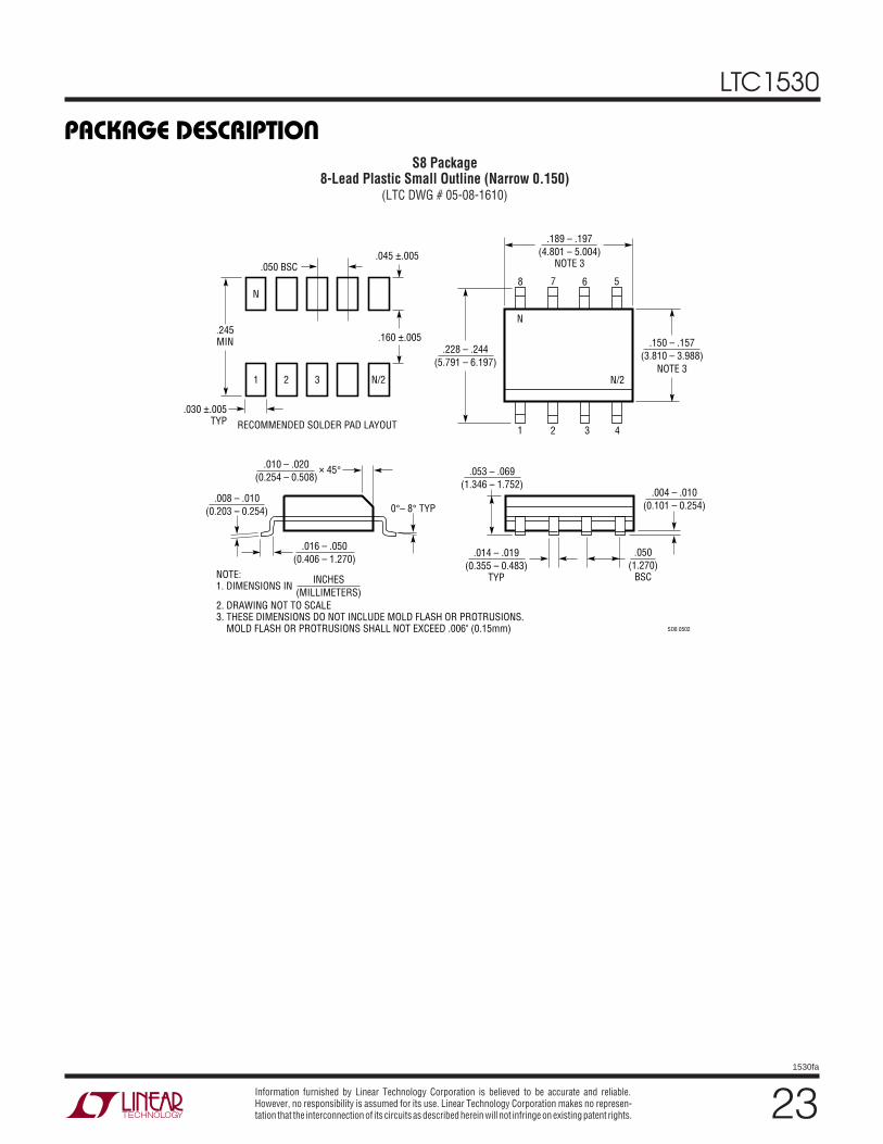
PACKAGE DESCRIPTION
U
S8 Package8-Lead Plastic Small Outline (Narrow 0.150)
(LTC DWG # 05-08-1610)
Information furnished by Linear Technology Corporation is believed to be accurate and reliable.However, no responsibility is assumed for its use. Linear Technology Corporation makes no represen-tation that the interconnection of its circuits as described herein will not infringe on existing patent rights.
.016 – .050(0.406 – 1.270)
.010 – .020(0.254 – 0.508)
× 45°
0°– 8° TYP.008 – .010
(0.203 – 0.254)
SO8 0502
.053 – .069(1.346 – 1.752)
.014 – .019(0.355 – 0.483)
TYP
.004 – .010(0.101 – 0.254)
.050(1.270)
BSC
1
N
2 3 4
N/2
.150 – .157(3.810 – 3.988)
NOTE 3
8 7 6 5
.189 – .197(4.801 – 5.004)
NOTE 3
.228 – .244(5.791 – 6.197)
.245MIN
N
1 2 3 N/2
.160 ±.005
RECOMMENDED SOLDER PAD LAYOUT
.045 ±.005 .050 BSC
.030 ±.005 TYP
INCHES(MILLIMETERS)
NOTE:1. DIMENSIONS IN
2. DRAWING NOT TO SCALE3. THESE DIMENSIONS DO NOT INCLUDE MOLD FLASH OR PROTRUSIONS. MOLD FLASH OR PROTRUSIONS SHALL NOT EXCEED .006" (0.15mm)
24
LTC1530
1530fa
LT/TP 1002 1K REV A • PRINTED IN USA
LINEAR TECHNOLOGY CORPORATION 1998
TYPICAL APPLICATION
U
Linear Technology Corporation1630 McCarthy Blvd., Milpitas, CA 95035-7417(408) 432-1900 FAX: (408) 434-0507 www.linear.com
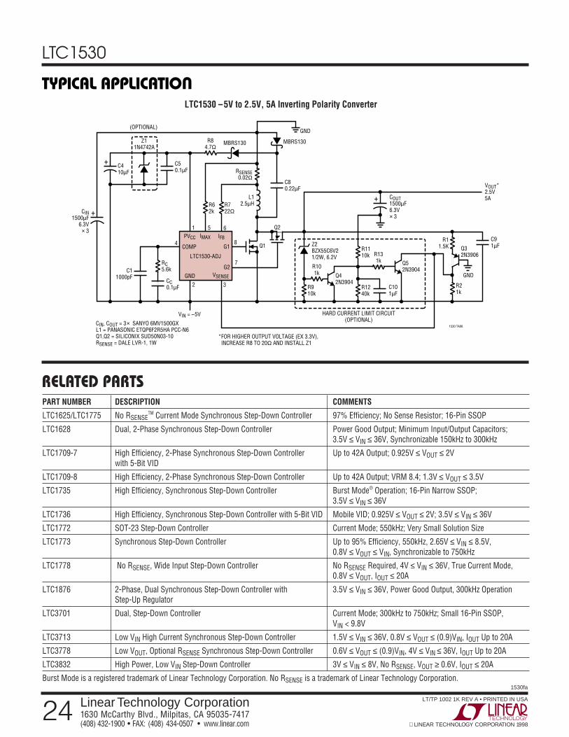
LTC1530 –5V to 2.5V, 5A Inverting Polarity Converter
RELATED PARTS
C101µF
C50.1µF
C410µF
COUT1500µF6.3V× 3
L12.5µH
RSENSE0.02Ω
Q42N3904
Q52N3904
R910k
R1110k
R1240k
R101k
R131k
Z2BZX55C6V21/2W, 6.2V
PVCC
GND
VIN = –5V
LTC1530-ADJ
G2
1 5
2
4
7
6
8
3
COMP
IFBIMAX
G1
VSENSE
1530 TA06CIN, COUT = 3× SANYO 6MV1500GXL1 = PANASONIC ETQP6F2R5HA PCC-N6Q1,Q2 = SILICONIX SUD50N03-10RSENSE = DALE LVR-1, 1W
RC5.6k
R62k
R722Ω
CC0.1µF
Q1
Q2
GND
GND
Q32N3906
HARD CURRENT LIMIT CIRCUIT(OPTIONAL)
C11000pF
R11.5K
R21k
VOUT*2.5V5A
Z11N4742A
(OPTIONAL)
MBRS130R84.7Ω
MBRS130
+
C80.22µF
C91µF
+CIN
1500µF6.3V
× 3
+
*FOR HIGHER OUTPUT VOLTAGE (EX 3.3V), INCREASE R8 TO 20Ω AND INSTALL Z1
PART NUMBER DESCRIPTION COMMENTS
LTC1625/LTC1775 No RSENSETM Current Mode Synchronous Step-Down Controller 97% Efficiency; No Sense Resistor; 16-Pin SSOP
LTC1628 Dual, 2-Phase Synchronous Step-Down Controller Power Good Output; Minimum Input/Output Capacitors;3.5V ≤ VIN ≤ 36V, Synchronizable 150kHz to 300kHz
LTC1709-7 High Efficiency, 2-Phase Synchronous Step-Down Controller Up to 42A Output; 0.925V ≤ VOUT ≤ 2Vwith 5-Bit VID
LTC1709-8 High Efficiency, 2-Phase Synchronous Step-Down Controller Up to 42A Output; VRM 8.4; 1.3V ≤ VOUT ≤ 3.5V
LTC1735 High Efficiency, Synchronous Step-Down Controller Burst Mode® Operation; 16-Pin Narrow SSOP;3.5V ≤ VIN ≤ 36V
LTC1736 High Efficiency, Synchronous Step-Down Controller with 5-Bit VID Mobile VID; 0.925V ≤ VOUT ≤ 2V; 3.5V ≤ VIN ≤ 36V
LTC1772 SOT-23 Step-Down Controller Current Mode; 550kHz; Very Small Solution Size
LTC1773 Synchronous Step-Down Controller Up to 95% Efficiency, 550kHz, 2.65V ≤ VIN ≤ 8.5V,0.8V ≤ VOUT ≤ VIN, Synchronizable to 750kHz
LTC1778 No RSENSE, Wide Input Step-Down Controller No RSENSE Required, 4V ≤ VIN ≤ 36V, True Current Mode,0.8V ≤ VOUT, IOUT ≤ 20A
LTC1876 2-Phase, Dual Synchronous Step-Down Controller with 3.5V ≤ VIN ≤ 36V, Power Good Output, 300kHz OperationStep-Up Regulator
LTC3701 Dual, Step-Down Controller Current Mode; 300kHz to 750kHz; Small 16-Pin SSOP,VIN < 9.8V
LTC3713 Low VIN High Current Synchronous Step-Down Controller 1.5V ≤ VIN ≤ 36V, 0.8V ≤ VOUT ≤ (0.9)VIN, IOUT Up to 20A
LTC3778 Low VOUT, Optional RSENSE Synchronous Step-Down Controller 0.6V ≤ VOUT ≤ (0.9)VIN, 4V ≤ VIN ≤ 36V, IOUT Up to 20A
LTC3832 High Power, Low VIN Step-Down Controller 3V ≤ VIN ≤ 8V, No RSENSE, VOUT ≥ 0.6V, IOUT ≤ 20A
Burst Mode is a registered trademark of Linear Technology Corporation. No RSENSE is a trademark of Linear Technology Corporation.