features - welcome to delta group 20a, high efficiency power module hs2403 features: high power...
TRANSCRIPT

1
20A, High Efficiency Power Module
HS2403
FEATURES:
High Power Density Power Module
Maximum Load:20A(22A@ Note 8)
Input Voltage Range from 4.5V to 20.0V
Output Voltage Range from 0.8V to 5.5V
96% Peak Efficiency
Parallel Three Modules for 60A Output Current
with Forced Current Sharing
Current Mode Control
Protections (OCP, OVP, UVP, OTP, Non-latching)
Programmable Soft Start with Pre-bias Output
Start-Up
Programmable Switching Frequency
Power Good Indication
Stack-QFN Package (14.5mm*14.5mm*7.45mm)
Pb-free Available (RoHS compliant)
MSL 3, 245C Reflow
APPLICATIONS:
General Buck DC/DC Conversion
DC Distributed Power System
Telecom and Networking Equipments
Servers System
Cell Phones / PDAs / Palmtops
GENERAL DESCRIPTION:
The HS2403 is a high frequency, high power density
and complete DC/DC power module. The PWM
controller, power MOSFETs and most of support
components are integrated in one hybrid package.
Additional, a new patent technology is adopted to
stack power choke on the hybrid module in order to
achieve high power density.
The module allows a modular power supply design
where multiple modules can be connected in parallel
to achieve the desired output power capability if the
output power requirement cannot be provided by one
module. Besides, HS2403 is an easy to use DC/DC
power module, only input capacitors and output
capacitors need to design for all kinds of applications.
The compact package enables utilization of unused
space on the bottom of PC boards for needing highly
space density applications. The HS2403 is packaged
in a thermally enhanced, compact and low profile QFN
package suitable for automated assembly by standard
surface mount equipment. The HS2403 is Pb-free and
RoHS compliance.
TYPICAL APPLICATION CIRCUIT & PACKAGE:
TABLE 1: OUTPUT VOLTAGE SETTING
Vout 0.9V 1.0V 1.2V 1.5V 1.8V 2.5V 3.3V 5V
RFB (Ohm) 34.8k 23.2k 14k 8.66k 6.34k 3.83k 2.61k 1.62k
HS2403Power Module
VIN(+5V / +12V)
VOUT(0.8V~5.5V)
RFBSetting Output Voltage
CIN COUT
FBVDD
VIN VOUT
PGND
VOSEN+
VOSEN-
VSH
14.5mm
7.45mm
14.5mm
2
20A, High Efficiency Power Module
HS2403
ORDER INFORMATION:
Part Number Ambient Temp. Range (°C) Package
(Pb-Free) MSL Note
HS2403 -40 ~ +85 Stack-QFN 20Ld. Level 3 -
Order Code Packing Quantity
HS2403 Tray 90
HS2403-T Tape and reel 350
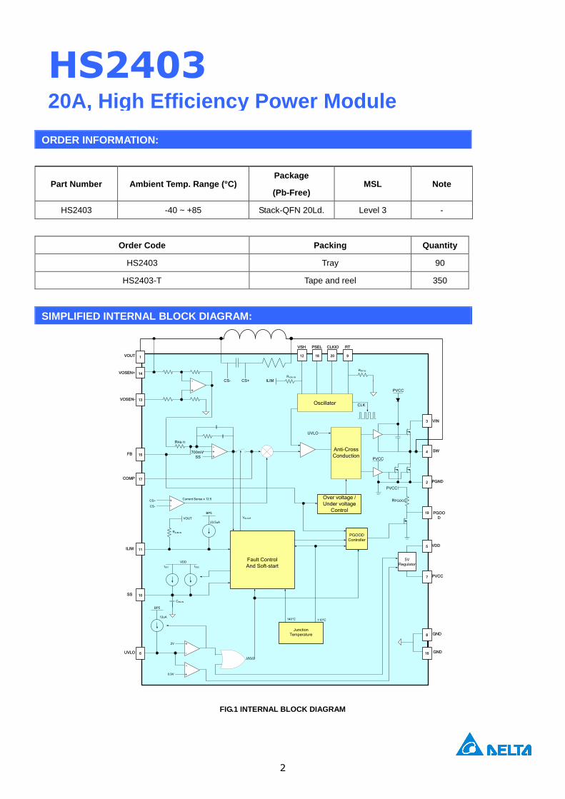
SIMPLIFIED INTERNAL BLOCK DIAGRAM:
3
4
2
Anti-Cross
Conduction
19
PVCC
PVCC
PVCC
5V
Regulator
5
PGOOD
Controller
Oscillator
12 18 20
CLK
UVLO
Over voltage /
Under voltage
Control
700mV
SS
14
13
15
17
CS+CS-
CS+
CS-
VSH
9
RTCLKIOPSEL
VOSEN+
1VOUT
VOSEN-
BP5
23.5uA
ILIM
11
FB
COMP
ILIM
Fault Control
And Soft-start
VSLAVE
VDD
10SS
ISS1 ISS2
BP5
12uA
RILIM-IN
VOUT
6
2V
0.9V
UVLO
Junction
Temperature
UVLO
VIN
SW
PGND
PGOO
D
VDD
7 PVCC
16
GND
RVSH-IN
8
GND
+
-
+
+
-
+
-
Current Sense x 12.5
+
+
-
-
140°C 110°C
RFB-TI
RPGOOD
RRT-IN
CSS-IN
FIG.1 INTERNAL BLOCK DIAGRAM

3
20A, High Efficiency Power Module
HS2403
PIN CONFIGURATION:
VOUT (1)
TP
D(1
)
PGND (2)
TPD(2)
(3) VIN
TP
D(3
)
(4) SW
TPD(4)
(5) VDD
(6) UVLO
(7) PVCCG
ND
(8
)
RT
(9
)
SS
(1
0)
ILIM
(1
1)
VS
H (
12
)
VO
SE
N-
(13
)
VO
SE
N+
(1
4)
FB
(1
5)
GN
D (
16
)
CO
MP
(1
7)
CLKIO (20)
PGOOD (19)
PSEL (18)
Top View
PIN DESCRIPTION:
Symbol Pin No. Description
VOUT
(TPD 1) 1
Power output pin. Connect to output and using for heat transferring to heat dissipation layer by Vias connection. Place the output capacitors as closely as possible to this pin.
PGND
(TPD 2) 2
Power ground pin. It needs to connect one or more ground plane directly and using for heat transferring to heat dissipation layer by Vias connection. Place the input ceramic type and output capacitors as closely as possible to this pin. If voltage spike stress and EMI considered, the snubber circuit can be as closely as possible connected to this pin that will absorb the spike and ringing.
VIN
(TPD 3) 3
Power input pin. It needs to connect input rail and using for heat transferring to heat dissipation layer by Vias connection. Place the input ceramic type capacitor as closely as possible to this pin.
SW
(TPD 4) 4
Switching node pin. Node of high-side and low-side MOSFETs and output inductor connection. Using for heat transferring to heat dissipation layer by Vias connection. For electrically, if voltage spike stress and EMI considered, the snubber circuit can be as closely as possible connected to this pin that will absorb the spike and ringing well.

4
20A, High Efficiency Power Module
HS2403
PIN DESCRIPTION: (Cont.)
Symbol Pin No. Description
VDD 5
Supply voltage pin for internal LDO device input. This LDO input can be supplied by external source or VIN directly. It needs to connect a 4.7ohms resistor and 2.2uF ceramic capacitor RC filter to power ground plane directly and place this capacitor as closely as possible to this pin.
UVLO 6
UVLO input for the device. A resistor divider from VDD sets the turn on voltage for the device. Below this voltage, the device is in a low quiescent current state. Pulling this pin to ground shuts down the device, and is used as system shutdown method.
PVCC 7
Output of internal LDO device. This is the power input for the drivers and bootstrap circuit. The 5.3V output on this pin is used for external circuitry as long as the total current required to drive the gate of the MOSFET and external loads is less than 50mA. Connect a 2.2uF capacitor from this pin to PGND.
GND 8, 16
Signal ground pin for overall signal reference used. No power level current should be allowed to flow through the GND pin copper areas on the board. Besides, it should have itself ground plane to cover the overall signal trace then connect to power ground plane directly by via.
RT 9
Switching frequency programming pin. It has an integrated internal 91k resistor (RRT-IN) between RT and GND pin for 300k Hz typical operation. One can also connect external resistor (RRT-EX) between this pin and GND pin to increase the switching frequency. Place this resistor as closely as possible to this pin. If this pin is connected to VDD or PVCC, the device is a clock slave and gets its time base from CLKIO of the clock master device. Phase addressing is done on PSEL.
SS 10
Soft-start input. This pin determines the startup ramp time for the converter as well as over current and other fault recovers timing. The voltage at this pin is applied as a reference to the error amplifier. While this voltage is below the precision 0.7V reference, it acts as the dominant reference to the error amp providing a closed loop startup. After is rises above the 0.7 V precision references, the 0.7V precision reference dominates and the output regulates at the programmed level. In case of an over current event, the converter attempts to restart after a period of time defined by seven soft-start cycles. Additionally this pin is used to configure the chip as a voltage loop master or slave. If the pin is tried to VDD or PVCC at power up, the device is in voltage loop slave mode. Otherwise, the device is a voltage loop master. It has an integrated internal 22nF capacitor (CSS-IN) between SS and GND pin for 1mS typical operation.
ILIM 11
Programs the over current limit of the device. Connecting a resistor from this pin to VSH and another to VOUT on the voltage loop master sets a voltage above VSH. COMP is not allowed to exceed this voltage. If the load current requirements force COMP to this level for seven clock cycles, an over current event is declared, and the system shuts down and enter a hiccup fault recover mode. The controller attempts to restart after a time period given by seven
soft-start cycles. It has an integrated internal 84.5 k resistor (RILIM-IN) between ILIM and VOUT pin for around 40A maximum current limits.

5
20A, High Efficiency Power Module
HS2403
PIN DESCRIPTION: (Cont.)
Symbol Pin No. Description
VSH 12
This pin is either an input or an output. If the device is configured as a voltage loop master the valley voltage is output on this pin and is distributed to the slave devices. If configured as a voltage loop slave, the master VSH pin is connected here and the device uses the master valley voltage reference to improve current sharing. Besides, this pin also multi-function with ILIM pin for over current setting
used. It has an integrated internal 2 Meg resistor (RVSH-IN) between VSH and ILIM pin for around 40A maximum current limits.
VOSEN- 13
Negative input to the remote sense amplifier. Amplifier is fixed of 1 differential mode and is used for output voltage sensing at the load to eliminate distribution drops. This pin should be directly connected to the point of load where the voltage regulation is required. CAUTION: Do not leave this pin open.
VOSEN+ 14
Positive input to the remote sense amplifier. Amplifier is fixed of 1 differential mode and is used for output voltage sensing at the load to eliminate distribution drops. This pin should be directly connected to the point of load where the voltage regulation is required. CAUTION: Do not leave this pin open.
FB 15 Feedback input. Connect resistor between this pin and ground for adjusting output voltage. Place this resistor as closely as possible to this pin. Normally this pin is at the reference voltage of 700mV.
COMP/EN 17 Output of the error amplifier. It has integrated the type 2 compensation networking circuit.
PSEL 18
Phase select pin. For a clock master, a resistor form this pin to GND determines the CLKIO output. When configured as a clock slave, a resistor from the pin to GND selects the phase relationship that the slave has with the master. Allowing this pin to float causes the slave to drop off line to share the phase when current demands are light for improved overall efficiency.
PGOOD 19
Power good output. This open drain output pulls low when the device is in any state other than in normal regulation. Active soft-start, UVLO, over current, under voltage, overvoltage or over temperature warning causes this output to pull low. It
has an integrated the pull high internal 10 k resistor (RPGOOD) between PVCC and this pin.
CLKIO 20 Clock and phase timing output while the device is configured as a clock master. In clock slave mode, the master CLKIO pin is connected to the slave CLKIO pin to provide time base information to the slave.
6
20A, High Efficiency Power Module
HS2403
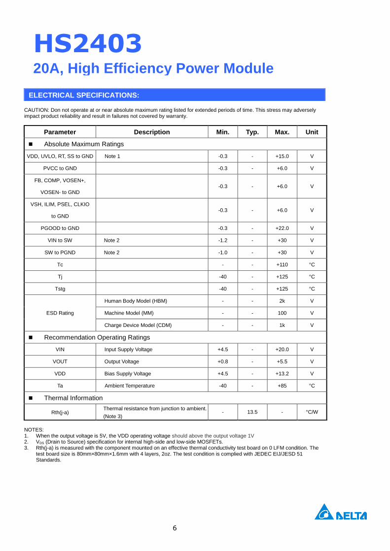
ELECTRICAL SPECIFICATIONS: CAUTION: Don not operate at or near absolute maximum rating listed for extended periods of time. This stress may adversely impact product reliability and result in failures not covered by warranty.
NOTES: 1. When the output voltage is 5V, the VDD operating voltage should above the output voltage 1V 2. VDS (Drain to Source) specification for internal high-side and low-side MOSFETs. 3. Rth(j-a) is measured with the component mounted on an effective thermal conductivity test board on 0 LFM condition. The
test board size is 80mm×80mm×1.6mm with 4 layers, 2oz. The test condition is complied with JEDEC EIJ/JESD 51 Standards.
Parameter Description Min. Typ. Max. Unit
Absolute Maximum Ratings
VDD, UVLO, RT, SS to GND Note 1 -0.3 - +15.0 V
PVCC to GND -0.3 - +6.0 V
FB, COMP, VOSEN+,
VOSEN- to GND -0.3 - +6.0 V
VSH, ILIM, PSEL, CLKIO
to GND -0.3 - +6.0 V
PGOOD to GND -0.3 - +22.0 V
VIN to SW Note 2 -1.2 - +30 V
SW to PGND Note 2 -1.0 - +30 V
Tc - - +110 °C
Tj -40 - +125 °C
Tstg -40 - +125 °C
ESD Rating
Human Body Model (HBM) - - 2k V
Machine Model (MM) - - 100 V
Charge Device Model (CDM) - - 1k V
Recommendation Operating Ratings
VIN Input Supply Voltage +4.5 - +20.0 V
VOUT Output Voltage +0.8 - +5.5 V
VDD Bias Supply Voltage +4.5 - +13.2 V
Ta Ambient Temperature -40 - +85 °C
Thermal Information
Rth(j-a) Thermal resistance from junction to ambient.
(Note 3) - 13.5 - °C/W
7
20A, High Efficiency Power Module
HS2403
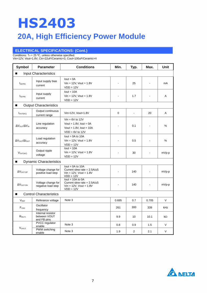
ELECTRICAL SPECIFICATIONS: (Cont.) Conditions: TA = 25 ºC, unless otherwise specified. Vin=12V, Vout=1.8V, Cin=22uF/Ceramic×3, Cout=100uF/Ceramic×4
Symbol Parameter Conditions Min. Typ. Max. Unit
Input Characteristics
IQ(VIN)
Input supply bias
current
Iout = 0A
Vin = 12V, Vout = 1.8V
VDD = 12V
- 25 - mA
IS(VIN) Input supply
current
Iout = 10A
Vin = 12V, Vout = 1.8V
VDD = 12V
- 1.7 - A
Output Characteristics
IOUT(DC) Output continuous
current range Vin=12V, Vout=1.8V 0 - 20 A
ΔVOUT/ΔVIN Line regulation
accuracy
Vin = 6V to 12V
Vout = 1.8V, Iout = 0A
Vout = 1.8V, Iout = 10A
VDD = 6V to 12V
- 0.1 - %
ΔVOUT/ΔIOUT Load regulation
accuracy
Iout = 0A to 10A
Vin = 12V, Vout = 1.8V
VDD = 12V
- 0.5 - %
VOUT(AC) Output ripple
voltage
Iout = 10A
Vin = 12V, Vout = 1.8V
VDD = 12V
- 30 - mVp-p
Dynamic Characteristics
ΔVOUT-DP Voltage change for positive load step
Iout = 0A to 10A Current slew rate = 2.5A/uS Vin = 12V, Vout = 1.8V VDD = 12V
- 140 - mVp-p
ΔVOUT-DN Voltage change for negative load step
Iout = 10A to 0A Current slew rate = 2.5A/uS Vin = 12V, Vout = 1.8V VDD = 12V
- 140 - mVp-p
Control Characteristics
VREF Referance voltage Note 3 0.695 0.7 0.705 V
FOSC Oscillator
frequency 261 300 339 kHz
RFB-TI Internal resistor between VOUT and FB pins
9.9 10 10.1 k
VUVLO
PVCC regulator enable
Note 3 0.8 0.9 1.5 V
PWM switching enable
Note 3 1.9 2 2.1 V

8
20A, High Efficiency Power Module
HS2403
ELECTRICAL SPECIFICATIONS: (Cont.) Conditions: TA = 25 ºC, unless otherwise specified. Vin=12V, Vout=1.8V, Cin=22uF/Ceramic×3, Cout=100uF/Ceramic×4
NOTES: 4. Parameters guaranteed by PWM IC vendor design and test prior to module assembly.
Symbol Parameter Conditions Min. Typ. Max. Unit
Control Characteristics
RPGOOD Internal resistor between PVCC and PGOOD pins
9.9 10 10.1 k
VFBPG-H PGOOD upper threshold voltage
Note 3 0.764 0.787 0.798 V
VFBPG-L PGOOD lower threshold voltage
Note 3 0.591 0.611 0.626 V
VPG-H PGOOD voltage High
PGOOD Open / No Fault - PVCC - V
VPG-L PGOOD voltage Low
PGOOD Open / Fault - 0.35 0.4 V
CSS-IN Internal capacitor between SS and GND pins
19.8 22 24.2 nF
ISS1 Soft start current source 1
Note 3 6.5 7.5 8.2 uA
ISS2 Soft start current source 2
Note 3 12 15 17 uA
Fault Protection
VFB-U FB under voltage threshold Note 3 565 580 595 mV
VFB-O FB over voltage threshold Note 3 792 810 828 mV
TTSD Shutdown
temperature Note 3 (Tj of internal PWM IC) 126 135 144 ℃
9
20A, High Efficiency Power Module
HS2403
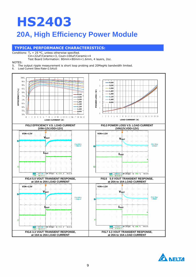
TYPICAL PERFORMANCE CHARACTERISTICS:
Conditions: TA = 25 ºC, unless otherwise specified. Cin=22uF/Ceramic× 3, Cout=100uF/Ceramic× 4 Test Board Information: 80mm× 80mm× 1.6mm, 4 layers, 2oz.
NOTES: 5. The output ripple measurement is short loop probing and 20MegHz bandwidth limited. 6. Load Current Slew Rate=2.5A/uS
FIG.2 EFFICIENCY V.S. LOAD CURRENT
(VIN=12V,VDD=12V) FIG.3 POWER LOSS V.S. LOAD CURRENT
(VIN12V,VDD=12V)
FIG.4 5.0 VOUT TRANSIENT RESPONSE,
at 10A to 20A LOAD CURRENT FIG.5 5.0 VOUT TRANSIENT RESPONSE,
at 20A to 10A LOAD CURRENT
FIG.6 3.3 VOUT TRANSIENT RESPONSE,
at 10A to 20A LOAD CURRENT FIG.7 3.3 VOUT TRANSIENT RESPONSE,
at 20A to 10A LOAD CURRENT
VOUT
IOUT
VOUT
IOUT
VOUT
IOUT
VOUT
IOUT
VIN=12V VIN=12V
VIN=12V VIN=12V

10
20A, High Efficiency Power Module
HS2403
TYPICAL PERFORMANCE CHARACTERISTICS:
Conditions: TA = 25 ºC, unless otherwise specified. Cin=22uF/Ceramic×3, Cout=100uF/Ceramic×4 Test Board Information: 80mm×80mm×1.6mm, 4 layers, 2oz.
FIG.8 1.8 VOUT TRANSIENT RESPONSE,
at 10A to 20A LOAD CURRENT FIG.9 1.8 VOUT TRANSIENT RESPONSE,
at 20A to 10A LOAD CURRENT
FIG.10 1.0 VOUT TRANSIENT RESPONSE,
at 10A to 20A LOAD CURRENT FIG.11 1.0 VOUT TRANSIENT RESPONSE,
at 20A to 10A LOAD CURRENT
VOUT
IOUT
VOUT
IOUT
VOUT
IOUT
VOUT
IOUT
VIN=12V VIN=12V
VIN=12V VIN=12V

11
20A, High Efficiency Power Module
HS2403
TYPICAL PERFORMANCE CHARACTERISTICS:
Conditions: TA = 25 ºC, unless otherwise specified. Cin=22uF/Ceramic×3, Cout=100uF/Ceramic×4 Test Board Information: 80mm×80mm×1.6mm, 4 layers, 2oz.
NOTES: 7. The output ripple measurement is short loop probing and 20MegHz bandwidth limited.
FIG.12 5.0VOUT OUTPUT RIPPLE, at 10A LOAD CURRENT
FIG.13 5.0VOUT OUTPUT RIPPLE, at 20A LOAD CURRENT
FIG.14 3.3VOUT OUTPUT RIPPLE,
at 10A CURRENT LOAD FIG.15 3.3VOUT OUTPUT RIPPLE,
at 20A LOAD CURRENT
FIG.16 1.8VOUT OUTPUT RIPPLE,
at 10A LOAD CURRENT FIG.17 1.8VOUT OUTPUT RIPPLE,
at 20A LOAD CURRENT
VOUT VOUT
VOUT VOUT
VOUT VOUT
VIN=12V VIN=12V
VIN=12V
VIN=12V
VIN=12V VIN=12V

12
20A, High Efficiency Power Module
HS2403
APPLICATIONS INFORMATION:
REFERENCE CIRCUIT FOR GENERAL APPLICATION:
Individual Application
The Figure 18 shows the HS2403 application schematics for input voltage +5V or +12V. The VDD pin can connect
to input supply directly by using a RC filter. If input voltage larger then +13.2V, please place a Zener diode between
VDD and GND.
RT
SS
VSH
VINVOUT
GND
VIN (+5V / +12V) VOUT
VDD
PVCC
UVLO
FB
VOSEN+
VOSEN-
FIG.18 TYPICAL APPLICATION WITH SINGLE POWER SUPPLY
Safety Considerations
Certain applications and/or safety agencies may require fuses at the inputs of power conversion components.
Fuses should also be used when there is the possibility of sustained input voltage reversal which is not current
limited. For greatest safety, we recommend a fast blow fuse installed in the ungrounded input supply line. The
installer must observe all relevant safety standards and regulations. For safety agency approvals, install the
converter in compliance with the end-user safety standard.

13
20A, High Efficiency Power Module
HS2403
APPLICATIONS INFORMATION: (Cont.)
Single Output with 2-Phases Interleaved Parallel Application
The main benefits of using the HS2403 is the ability to parallel output power stages to achieve higher output
currents and stack on controllers as needed. Phasing information is also shared among the controllers to
minimize input ripple and RMS current in the input stage capacitors. Figure 19 show the controller
configuration connections to implement a single output stacked configuration for 40A load sharing. The
master controller is configured as a CLK master and as a voltage control loop master (SS and RT pin
connections). The slave controllers are configured as CLK slaves (RT pin tied to VDD) and as voltage control
loop slaves (SS pin tied to VDD).The PSEL pin selects the CLKIO operating mode for the device. The PSEL
phase programming states defined in Table 2. In any system configured to have a CLK master and CLK
slaves, a 10-kΩ resistor connected from CLKIO to GND is required.
PSEL
VDD
RT
SS
CLKIOVSHCOMP
VINVOUT
GND
SHARING BUS
VIN
PSEL
RT
SSCLKIOVSHCOMP
VIN
VOUT
GND
MASTER
SLAVE
VOUT
PS
EL1
PSEL2
UVLO
VDD
UVLO
FBPVCC
PVCC
VOSEN+
VOSEN-
FIG.19 TYPICAL APPLICATION WITH 2-PHASES Parallel OPERATION
TABLE 2. PSEL PHASE PROGRAMMING
8-Phase Angle for Slave
PSEL1
(k) Phase Angle Stand by 45˚ 90˚ 135˚ 180˚ 215˚ 270˚ 315˚
Open PSEL 2 (k) Open 0 14.7 29.4 47 68 95.3 127
6-Phase Angle for Slave
PSEL1
(k) Phase Angle Stand by 0˚ 60˚ 120˚ 180˚ 240˚ 300˚ -
29.4 PSEL 2 (k) Open 95.3 0 14.7 29.4 47 68 -
14
20A, High Efficiency Power Module
HS2403
APPLICATIONS INFORMATION: (Cont.)
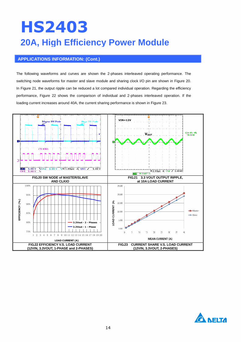
The following waveforms and curves are shown the 2-phases interleaved operating performance. The
switching node waveforms for master and slave module and sharing clock I/O pin are shown in Figure 20.
In Figure 21, the output ripple can be reduced a lot compared individual operation. Regarding the efficiency
performance, Figure 22 shows the comparison of individual and 2-phases interleaved operation. If the
loading current increases around 40A, the current sharing performance is shown in Figure 23.
FIG.20 SW NODE of MASTER/SLAVE AND CLKIO
FIG.21 3.3 VOUT OUTPUT RIPPLE, at 10A LOAD CURRENT
75%
80%
85%
90%
95%
100%
1 2 3 4 5 6 7 8 9 10 11 12 13 14 15 16 17 18 19 20
LOAD CURRENT (A)
EFFIC
IE
NC
Y (
%)
3.3Vout - 2 - Phases
3.3Vout - 1 - Phase
FIG.22 EFFICIENCY V.S. LOAD CURRENT
(12VIN, 3.3VOUT, 1-PHASE and 2-PHASES) FIG.23 CURRENT SHARE V.S. LOAD CURRENT
(12VIN, 3.3VOUT, 2-PHASES)
VOUT
VIN=12V

15
20A, High Efficiency Power Module
HS2403
APPLICATIONS INFORMATION: (Cont.)
Dual Outputs with Clock Synchronous
A connection diagram for two controllers sharing phase information and synchronized to each other but having
different output voltages is shown in Figure 24. The controllers are all control loop masters (SS not pulled to VDD)
and control their own output voltages independently. One device is configured as a CLK master (RT not tied to VDD)
and is the clock generator for the CLK slaves. Picking the PSEL resistors is the same as before in TABLE 2. If one
of the CLK slaves experiences a fault, that converter only shuts down, and enters the hiccup restart mode. If the
CLK master controller senses an over current, it stops sending CLKIO pulses to the slaves, causing them to stop.
The master then enters a hiccup recovery mode. In any system configured to have a CLK master and CLK slaves, a
10-kΩ resistor connected from CLKIO to GND is required.
PSEL
RTSS
CLKIO
VSH
FB
VINVOUT
GND
VIN
PSEL
RT
SSCLKIOVSH
FB
VINVOUT
GND
MASTER
SLAVE
VOUT 1
PS
EL1
PSEL2
SHARING BUS
VOUT 2
VDD
UVLO
PVCC
PVCC
VDD
UVLO
VOSEN+
VOSEN-
VOSEN-
VOSEN+
FIG.24 TYPICAL APPLICATION FOR DUAL OUTPUTS OPERATION

16
20A, High Efficiency Power Module
HS2403
APPLICATIONS INFORMATION: (Cont.)
The following waveforms and curves are shown the dual outputs with clock synchronous operating performance.
The input, each output ripple, and switching node waveforms are shown in Figure 25, 26, 27, and 28.
FIG.25 INPUT AND OUTOUT RIPPLE FIG.26 SW NODE of MASTER/SLAVE
AND INPUT RIPPLE
FIG.27 INPUT AND OUTPUT RIPPLE (5.0VOUT@0A, 3.3VOUT@10A)
FIG.28 INPUT AND OUTPUT RIPPLE (5.0VOUT@10A, 3.3VOUT@0A)
VIN=12V
VIN=12V VIN=12V

17
20A, High Efficiency Power Module
HS2403
APPLICATIONS INFORMATION: (Cont.)
PROGRAMMING OUTPUT VOLTAGE:
The HS2403 has an internal 0.7V±1.0% reference voltage. It only programs the dividing resistance RFB which
respects to FB pin and GND. The output voltage can be calculated as shown in Equation 1 and the resistance
according to typical output voltage is shown in TABLE 1.
(EQ.1)
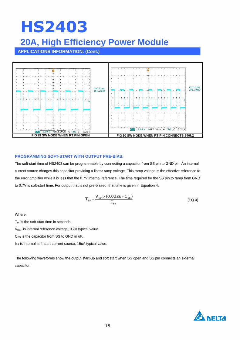
PROGRAMMING SWITCHING FREQUENCY:
Considering the efficiency and noise immunity, the HS2403 has setting the typical 300k Hz for initial operating
frequency; its internal configuration resistor for operating frequency (RRT-IN) is 91k ohms. If there is low output ripple
noise or output capacitance limits application, the operating frequency can be increased by configuring an external
resistor to RT pin in parallel. The calculation formula for operating frequency is shown as below.
(EQ.2)
Where:
Fsw is the desired switching frequency in kHz.
RRT is equivalent resistance for switching frequency setting in kohms and is calculated between RT and GND pins.
The HS2403 has integrated 91k resistance (RRT-IN). Therefore, the equivalent resistance of RRT can be expressed
in Equation 3.
(EQ.3)
The following waveforms show the 300k Hz typical switching frequency (Let RT pin open) and 400k Hz which RT pin
connects a 240k resistor to GND.
FBR
10k10.7VOUT
5.355Fsw
102.824
Fsw
103.675R
4
2
5
RT
IN-RTEX-RT
IN-RTEX-RTRT
RR
RRR
18
20A, High Efficiency Power Module
HS2403
APPLICATIONS INFORMATION: (Cont.)
FIG.29 SW NODE WHEN RT PIN OPEN FIG.30 SW NODE WHEN RT PIN CONNECTS 240k
PROGRAMMING SOFT-START WITH OUTPUT PRE-BIAS:
The soft-start time of HS2403 can be programmable by connecting a capacitor from SS pin to GND pin. An internal
current source charges this capacitor providing a linear ramp voltage. This ramp voltage is the effective reference to
the error amplifier while it is less that the 0.7V internal reference. The time required for the SS pin to ramp from GND
to 0.7V is soft-start time. For output that is not pre-biased, that time is given in Equation 4.
(EQ.4)
Where:
Tss is the soft-start time in seconds.
VREF is internal reference voltage, 0.7V typical value.
CSS is the capacitor from SS to GND in uF.
ISS is internal soft-start current source, 15uA typical value.
The following waveforms show the output start-up and soft start when SS open and SS pin connects an external
capacitor.
SS
SSREFSS
I
C0.022uVT

19
20A, High Efficiency Power Module
HS2403
APPLICATIONS INFORMATION: (Cont.)
FIG.31 OUTPUT AND SS WHEN SS PIN OPEN
FIG.32 OUTPUT AND SS WHEN SS PIN CONNECT
47nF
Considering the output of HS2403 has a pre-existing voltage, the internal soft-start current source is held to a lower
value than normal until the PWM signal becomes active. This occurs as the SS pin voltage exceeds the FB pin
voltage and the COMP pin moves up into the ramp rang, causing the first pulse. At that point, the internal soft-start
current is shifted to 15uA nominal. The Figure 33 and Figure 34 illustrate this operation.
0
FB
0.7V
VDDSS
0
RegulationVOUT
VPre-Bias
T0 T1 T2
Time
Time
ISS2
ISS1
FIG.33 SOFT-SATRT WAVEFORM WITH PRE-BIASED OUTPUT
VOUT
SS
1mS
VOUT
SS
3.22mS

20
20A, High Efficiency Power Module
HS2403
APPLICATIONS INFORMATION: (Cont.)
+
-
+FB
SS
VOUT VREF=0.7V
Error AmpRFB-TI 10k
0.022uFRFB CSS
ISS1=7.5uAISS2=15uA
PWM / Fault
HS20116
FIG.34 SOFT-SATRT IMPLEMENTION
Based on Figure 34, the soft-start time with output pre-existing voltage can be calculated as below.
(EQ.5)
(EQ.6)
(EQ.7)
Where:
T1 is the time to the first PWM pulse in seconds.
T2 is the time from the first PWM pulse until regulation in seconds.
TSS is the total soft-start time.
CSS is the capacitor from SS to GND in uF.
ISS1 is internal soft-start current source, 7.5uA typical value.
ISS2 is internal soft-start current source, 15uA typical value.
VREF is internal reference voltage, 0.7V typical value.
RFB-TI is internal voltage dividing resistor, 10k ohms typical value.
RFB is external voltage dividing resistor.
FBTIFB
FBBiasPre
SS1
SS1
RR
RV
I
C0.022uT
FBTIFB
FBBiasPreREF
SS2
SS2
RR
RVV
I
C0.022uT
21SS TTT
21
20A, High Efficiency Power Module
HS2403
APPLICATIONS INFORMATION: (Cont.)
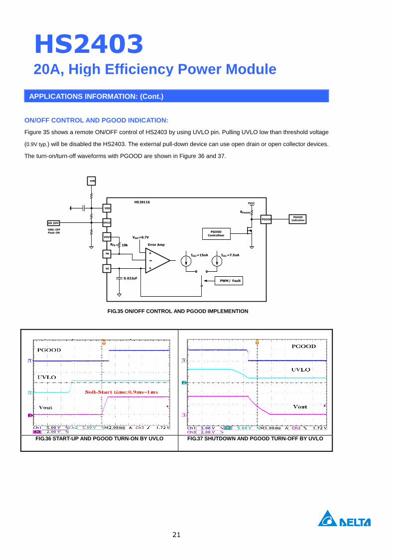
ON/OFF CONTROL AND PGOOD INDICATION:
Figure 35 shows a remote ON/OFF control of HS2403 by using UVLO pin. Pulling UVLO low than threshold voltage
(0.9V typ.) will be disabled the HS2403. The external pull-down device can use open drain or open collector devices.
The turn-on/turn-off waveforms with PGOOD are shown in Figure 36 and 37.
+
-
+FB
SS
VOUT VREF=0.7V
Error AmpRFB-TI 10k
0.022uF
ISS1=7.5uAISS2=15uA
PWM / Fault
HS20116
UVLO
VDD
VIN
ON /OFF
GND: OFFFloat: ON
PGOOD
PGOODControlloer
PVCC
RPGOOD
PGOOD Indication
FIG.35 ON/OFF CONTROL AND PGOOD IMPLEMENTION
FIG.36 START-UP AND PGOOD TURN-ON BY UVLO
FIG.37 SHUTDOWN AND PGOOD TURN-OFF BY UVLO
22
20A, High Efficiency Power Module
HS2403
APPLICATIONS INFORMATION: (Cont.)
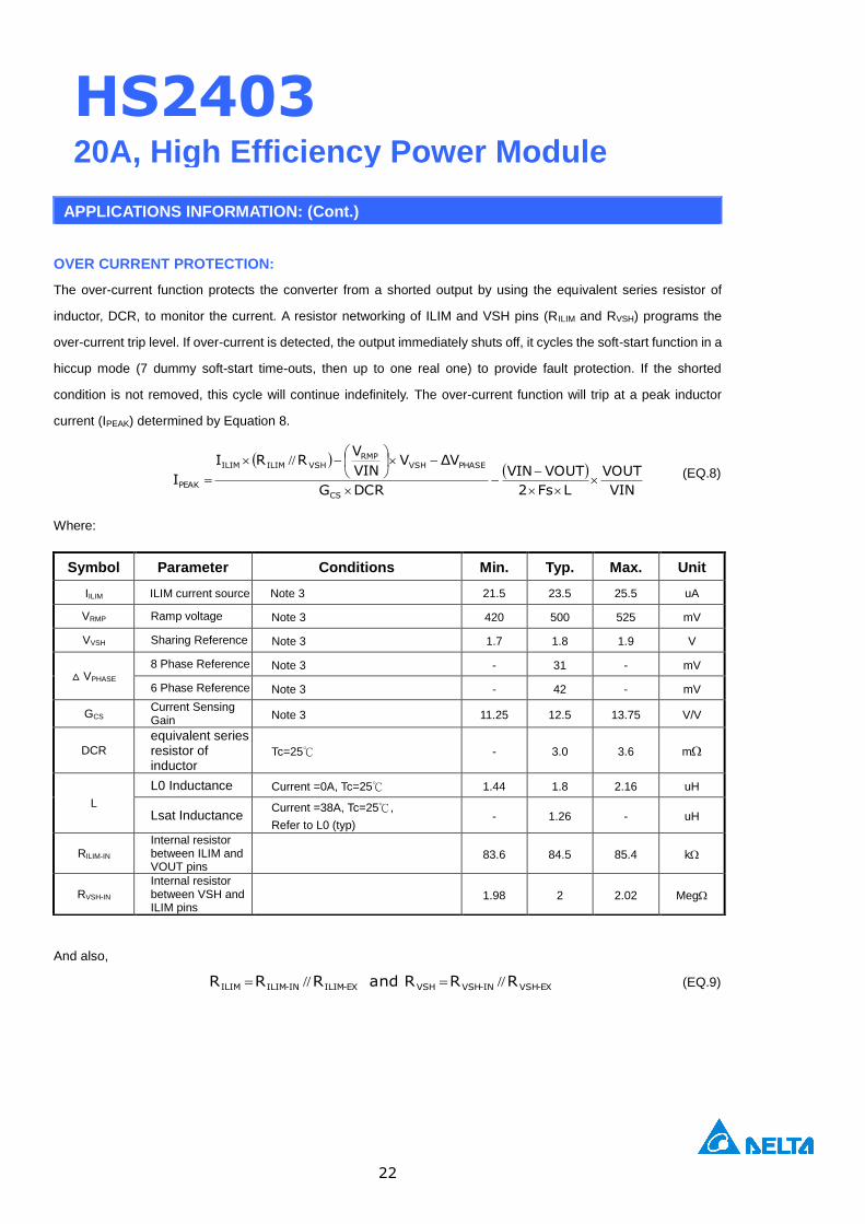
OVER CURRENT PROTECTION:
The over-current function protects the converter from a shorted output by using the equivalent series resistor of
inductor, DCR, to monitor the current. A resistor networking of ILIM and VSH pins (RILIM and RVSH) programs the
over-current trip level. If over-current is detected, the output immediately shuts off, it cycles the soft-start function in a
hiccup mode (7 dummy soft-start time-outs, then up to one real one) to provide fault protection. If the shorted
condition is not removed, this cycle will continue indefinitely. The over-current function will trip at a peak inductor
current (IPEAK) determined by Equation 8.
(EQ.8)
Where:
And also,
(EQ.9)
Symbol Parameter Conditions Min. Typ. Max. Unit
IILIM ILIM current source Note 3 21.5 23.5 25.5 uA
VRMP Ramp voltage Note 3 420 500 525 mV
VVSH Sharing Reference Note 3 1.7 1.8 1.9 V
△ VPHASE 8 Phase Reference Note 3 - 31 - mV
6 Phase Reference Note 3 - 42 - mV
GCS Current Sensing Gain Note 3 11.25 12.5 13.75 V/V
DCR
equivalent series resistor of inductor
Tc=25℃ - 3.0 3.6 m
L
L0 Inductance Current =0A, Tc=25℃ 1.44 1.8 2.16 uH
Lsat Inductance Current =38A, Tc=25℃,
Refer to L0 (typ) - 1.26 - uH
RILIM-IN Internal resistor between ILIM and VOUT pins
83.6 84.5 85.4 k
RVSH-IN Internal resistor between VSH and ILIM pins
1.98 2 2.02 Meg
VIN
VOUT
LFs2
VOUTVIN
DCRG
ΔVVVIN
VRRI
ICS
PHASEVSHRMP
VSHILIMILIM
PEAK
//
RRR and RRR EX-VSHIN-VSHVSHEX-ILIMIN-ILIMILIM ////
23
20A, High Efficiency Power Module
HS2403
APPLICATIONS INFORMATION: (Cont.)
INPUT AND OUTPUT CAPACITORS:
Place the decoupled ceramic capacitors to control the high frequency voltage overshoot and bulk capacitor to supply
the current needed each time module turns-on. The important parameters for bulk capacitor are voltage rating and
the RMS current rating. For reliable operation, the bulk capacitor selects the voltage and current rating above
maximum input voltage and highest RMS current required.
The bulk output capacitors COUT is chosen with low enough effective series resistance (ESR) to meet the output
voltage ripple and transient requirements. COUT can be low ESR tantalum capacitor, low ESR polymer capacitor or
ceramic capacitor. The typical capacitance is 600uF and decupled ceramic output capacitors are used. Additional
output filtering may be required by the system designer, if further reduction of output ripple or dynamic transient
spike is required.
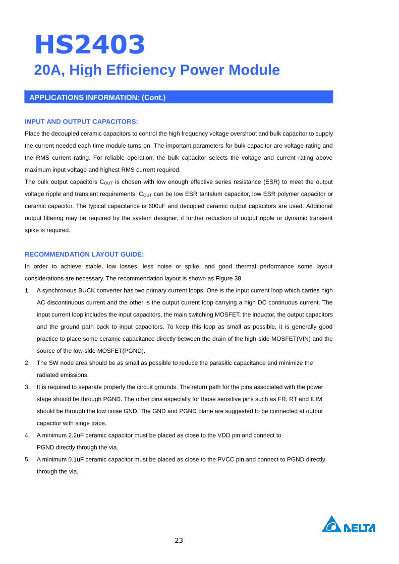
RECOMMENDATION LAYOUT GUIDE:
In order to achieve stable, low losses, less noise or spike, and good thermal performance some layout
considerations are necessary. The recommendation layout is shown as Figure 38.
1. A synchronous BUCK converter has two primary current loops. One is the input current loop which carries high
AC discontinuous current and the other is the output current loop carrying a high DC continuous current. The
input current loop includes the input capacitors, the main switching MOSFET, the inductor, the output capacitors
and the ground path back to input capacitors. To keep this loop as small as possible, it is generally good
practice to place some ceramic capacitance directly between the drain of the high-side MOSFET(VIN) and the
source of the low-side MOSFET(PGND).
2. The SW node area should be as small as possible to reduce the parasitic capacitance and minimize the
radiated emissions.
3. It is required to separate properly the circuit grounds. The return path for the pins associated with the power
stage should be through PGND. The other pins especially for those sensitive pins such as FR, RT and ILIM
should be through the low noise GND. The GND and PGND plane are suggested to be connected at output
capacitor with singe trace.
4. A minimum 2.2uF ceramic capacitor must be placed as close to the VDD pin and connect to
PGND directly through the via.
5. A minimum 0.1uF ceramic capacitor must be placed as close to the PVCC pin and connect to PGND directly
through the via.
24
20A, High Efficiency Power Module
HS2403
APPLICATIONS INFORMATION: (Cont.)
VIN
PGND
VOUT
GND
PGND
FIG.38 RECOMMENDATION LAYOUT (Top)
NOTES: 1. The trip values are tested at TA = 25 ºC, Cin=22uF/Ceramic×5, Cout=100uF/Ceramic×6.
Test Board Information:60mm×60mm×1.6mm, 4 layers, 2oz.

25
20A, High Efficiency Power Module
HS2403
APPLICATIONS INFORMATION: (Cont.)
THERMAL CONSIDERATIONS:
All of thermal testing condition is complied with JEDEC EIJ/JESD 51 Standards. Therefore, the test board size is
80mm×80mm×1.6mm with 4 layers, 2oz. The case temperature of module sensing point is shown as Figure 39.
Then Rth(j-a) is measured with the component mounted on an effective thermal conductivity test board on 0 LFM
condition. The HS2403 module is designed for using when the case temperature is below 110°C regardless the
change of output current, input/output voltage or ambient temperature. The de-rating load current in different output
voltage are shown in Figure 40, 41, 42, and 43. It would be convenient for user to confirm and estimate module’s
approximate performance according to actual operating conditions in beginning of design.
FIG.39 CASE TEMPERATURE SENSING POINT
FIG.40 12VIN/5.0VOUT DE-RATING CURVE FIG.41 12VIN/3.3VOUT DE-RATING CURVE
FIG.42 12VIN/1.8VOUT DE-RATING CURVE FIG.43 12VIN/0.9VOUT DE-RATING CURVE
26
20A, High Efficiency Power Module
HS2403
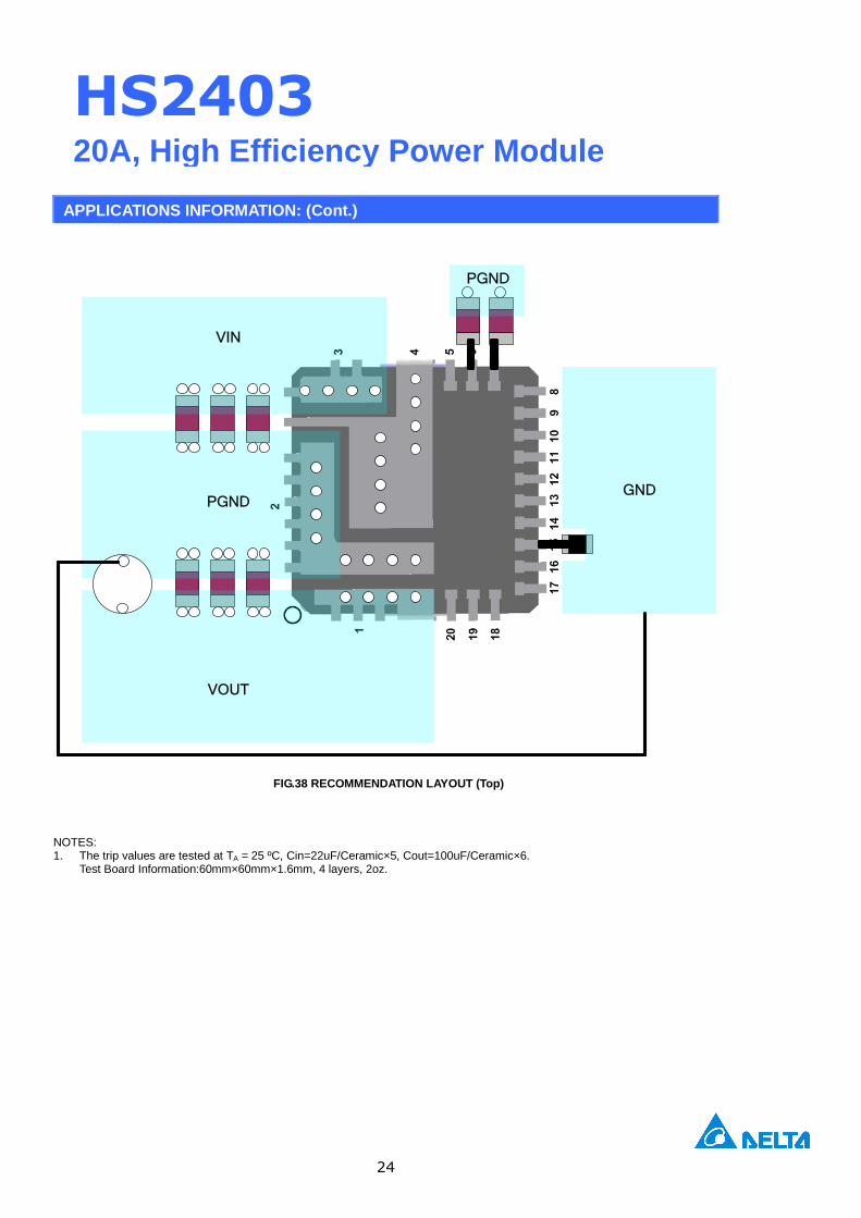
THERMAL PERFORMANCE (Cont.):
Force Air Flow Thermal Management for 22A Applications:
Some of applications will over 20A under forced air flow. Here is an example for 22A output current application when
the system has forced air flow to do the heat transferring. The thermal evaluation set-up by using wind tunnel is
shown as below.
PCBModule
Air Flow
200 mm
840mm
450mm
70mm
Air VelocityMeasured
80mm
150mm
Ambient Temp. Measured
75mm
Figure. 44 Thermal Measurement Set-up
There are two cases for thermal management reference according to difference PCB size and output voltage. The
measurement result is shown as below table.
TABLE 3 THERMAL MAGETMENT REFERENCE FOR 22A APPLICATION
Vin=12V / Vout=5 / PVCC=8V / Iout=22A When Case Temperature of module (Tc)=110℃
PCB Size (mm) Layer Copper Thickness (Oz) Ambient Temp. (℃) Air Velocity (LFM)
80 x 80 x 1.6 4 2 25 25
Vin=12V / Vout=5 / PVCC=8V / Iout=22A When Case Temperature of module (Tc)=85℃
35 x 20 x 1.2 4 2 25 585
Vin=12V / Vout=3.3 / PVCC=8V / Iout=22A When Case Temperature of module (Tc)=110℃
80 x 80 x 1.6 4 2 25 0
Vin=12V / Vout=3.3 / PVCC=8V / Iout=22A When Case Temperature of module (Tc)=85℃
35 x 20 x 1.2 4 2 25 535
NOTES: 8. The measurement result shown on table 3 is only for reference based on specific condition as Fig-44, not applied to the
overall applications. It may affect device reliability or cause permanent damage when the operation is beyond this recommendation. Needs to confirm with manufactory if condition will be changed.
27
20A, High Efficiency Power Module
HS2403
PACKAGE OUTLINE DRAWING:
Unit: mm
X4
X4
C1
C1

28
20A, High Efficiency Power Module
HS2403
REFLOW PARAMETERS:
Lead-free soldering process is a standard of making electronic products. Many solder alloys like Sn/Ag, Sn/Ag/Cu,
Sn/Ag/Bi and so on are used extensively to replace traditional Sn/Pb alloy. Here the Sn/Ag/Cu alloy (SAC) are
recommended for process. In the SAC alloy series, SAC305 is a very popular solder alloy which contains 3% Ag and
0.5% Cu. It is easy to get it. Figure 45 shows an example of reflow profile diagram. Typically, the profile has three
stages. During the initial stage from 70°C to 90°C, the ramp rate of temperature should be not more than 1.5°C/sec.
The soak zone then occurs from 100°C to 180°C and should last for 90 to 120 seconds. Finally the temperature
rises to 230°C to 245°C and cover 220°C in 30 seconds to melt the solder. It is noted that the time of peak
temperature should depend on the mass of the PCB board. The reflow profile is usually supported by the solder
vendor and user could switch to optimize the profile according to various solder type and various manufactures’
formula.
FIG.45 RECOMMENDATION REFLOW PROFILE

29
20A, High Efficiency Power Module
HS2403
STORAGE AND HANDLING:
MOISTURE BARRIER BAG:
Although POL module is a kind of package devices and its inner components are all protected by the package
compounds, it is still probably damaged during soldering process if moisture is absorbed into package. The modules
firstly are packed in a reel, and then an aluminum moisture barrier bag is used to pack the reel in order to prevent
moisture absorption. Silica gel is put into the aluminum moisture barrier bag as absorbent material.
STORAGE:
The POL module pack storage follows the JEDEC J-STD-033B01 and J-STD-020C standards. Table 4 is the floor
life and moisture sensitive level defined by JEDEC. POL module is classified into level 3. The floor life starts to
estimate while the aluminum moisture barrier bag is opened. Under the storage situation of 30°C/60% RH, the
device can keep 168 hours floor life after the pack opened. If there are unused POL modules remained, they should
be resealed in original moisture barrier bag as soon as possible. However, in case of the modules’ floor life
exceeding the defined time period, baking process will be necessary to dehumidify. The method is to bake the
module in an oven at 125°C/1% RH (e.g. hot nitrogen gas atmosphere) for 48 hours.
HANDLING AND OTHERS:
To protect the POL module and to make sure its normal use, something should be noticed as below.
1. Please handle the POL module carefully to avoid unnecessary mechanism stress on it. Improperly external
stress may cause unexpected damage.
2. The ESD wrist strap, ESD shoe strap or anti-electrostatic gloves are recommended to be used whenever
handling POL module.
3. If cleaning the module is necessary, please use alcohol or IPA solution to clean it under normal room
temperature. Avoid the use of unspecified solvent.

30
20A, High Efficiency Power Module
HS2403
STORAGE AND HANDLING: (Cont.)
TABLE 4 MOISTURE CLASSIFICATION LEVEL AND FLOOR LIFE
Level Floor Life (out of bag) at factory ambient ≦30°C/60% RH
or as stated
1 Unlimited at ≦30°C/85% RH
2 1 year
2a 4 weeks
3 168 hours
4 72 hours
5 48 hours
5a 24 hours
6 Mandatory bake before use. After bake, must be reflowed within the time limit
specified on the label.
31
20A, High Efficiency Power Module
HS2403
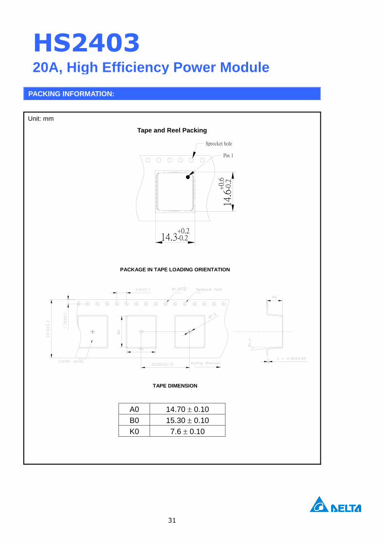
PACKING INFORMATION:
Unit: mm
Tape and Reel Packing
PACKAGE IN TAPE LOADING ORIENTATION
TAPE DIMENSION
A0 14.70 0.10
B0 15.30 0.10
K0 7.6 0.10
Pin 1
Sprocket hole
14.6
+0.
6-0
.2
14.3+0.2-0.2

32
20A, High Efficiency Power Module
HS2403
PACKING INFORMATION: (Cont.)
Unit: mm
W1=24.8 +0.6/-0.4
W2=30.2(MAX)
REEL DIMENSION
Peel Strength of Top Cover Tape
The peel speed shall be about 300mm/min.
The peel force of top cover tape shall between 0.1N to 1.3 N
165~180°
Top Cover Tape
0.1N~1.3N
33
20A, High Efficiency Power Module
HS2403
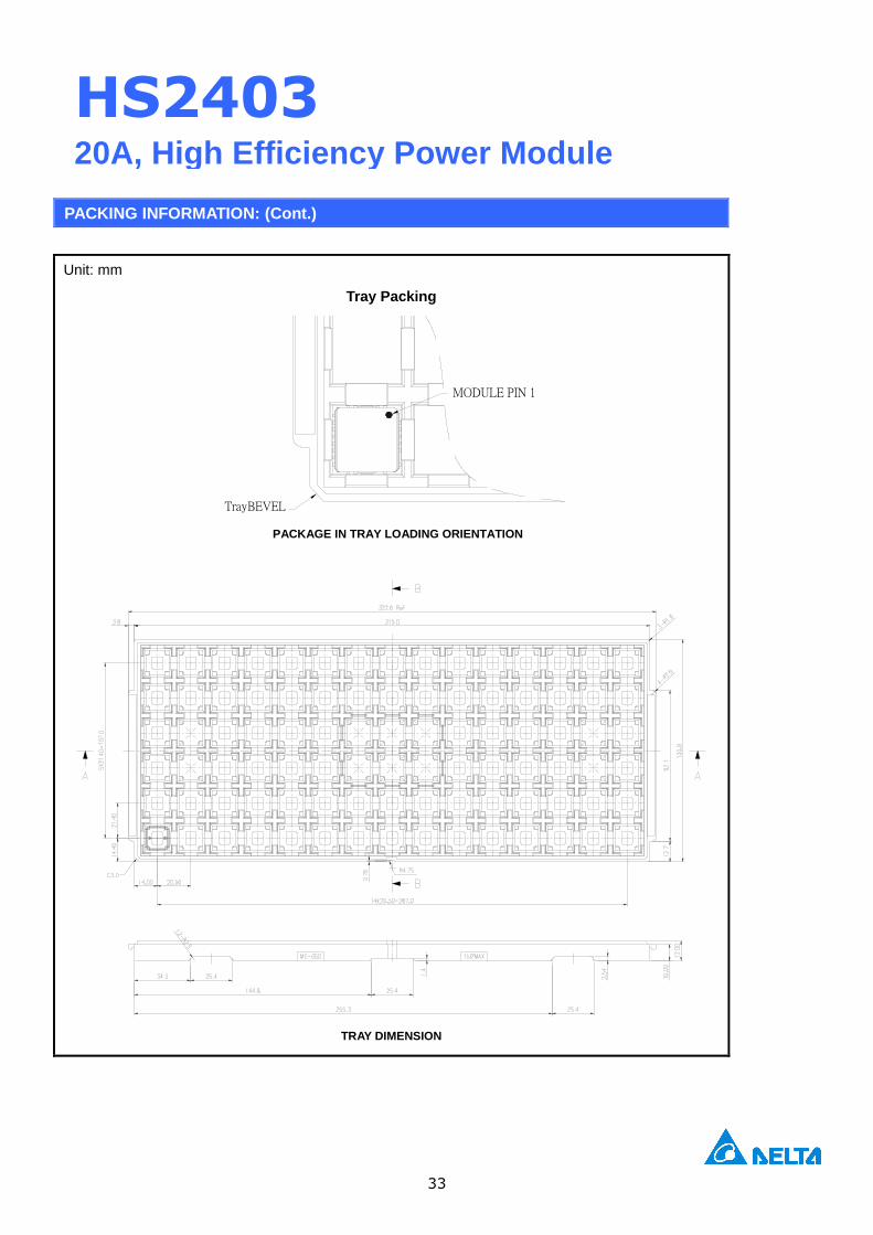
PACKING INFORMATION: (Cont.)
Unit: mm
Tray Packing
MODULE PIN 1
TrayBEVEL
PACKAGE IN TRAY LOADING ORIENTATION
B9
TRAY DIMENSION