ferroelectric hfo2 thin films for fefet memory devices
TRANSCRIPT

34TH ANNUAL MICROELECTRONIC ENGINEERING CONFERENCE, MAY 2016 1
Ferroelectric HfO2 Thin Filmsfor FeFET Memory Devices
Joseph F. McGlone
Abstract—Silicon-doped hafnium oxide has been shown toexhibit ferroelectric properties under the certain small thick-nesses with appropriate applied stress and annealing conditions.Utilizing Si:HfO2 as the dielectric with a TiN capping layer ina ferroelectric field-effect-transistor (FeFET) is promising as apotential emerging memory device due to the ease in integrationwith standard CMOS process flows. The process developed atRIT was successful in fabricating n-channel FeFETs of varyingdimensions. The work done here utilizes a 10 nm thick ALDSi:HfO2 film that has a remnant polarization of 10.34 µC/cm2
and an average memory window of 572.3 mV . The subthresholdcharacteristics were consistent in both the on and off state witha calculated subthreshold swing around 110 mV/dec.
Keywords—Ferroelectric Memory, Hafnium Dioxide, FeFET.
I. INTRODUCTION
B IG Data and data analytics are essential and growingsectors in modern day technology. Millions of users and
companies are creating massive amounts of data from personaldevices, health trackers, medical sensors, and environmentalsensors. The use and correct analysis of this data can havenumerous benefits to society, including uncovering impor-tant medical trends to help diagnose patients quickly andaccurately. With all of this increased data generation comesthe need for more storage space; increasing storage spacerequires more power, which ultimately has a negative effecton the environment. To compensate for these challenges, non-volatile memory devices are being widely studied to evaluatehigh-density and low-power opportunities in system memoryhierarchy for superior system performance.
One promising non-volatile memory device is a ferroelec-tric field effect transistor (FeFET). A FeFET stores memorythrough the remnant polarization state of the ferroelectric filmin the gate stack, causing shifts in the threshold voltage ofthe device. This change in threshold voltage is interpretedas different storage values. FeFETs have advantages suchas a simple one-transistor (1T) memory cell design with aread and write latency in the nanosecond range [1]. Typicalferroelectric memory devices use lead-based films, but lead-free ferroelectric thin film device design is a growing fieldand a strong contender in emerging memory technology.
A lead-free option is silicon-doped hafnium oxide (Si:HfO2)ferroelectric films which have been demonstrated to showexcellent potential as a competitive memory technology [2].Since HfO2 has already been adopted as a high-k gate di-electric material for state-of-the-art devices currently in mass
J. McGlone is with the Department of Electrical and MicroelectronicEngineering, Rochester Institute of Technology, Rochester, NY.
production, hafnium-based ferroelectric films can be easilyintegrated into a standard CMOS process flow. In additionto the ease of integration, Si:HfO2 has higher coercive fieldswhich allows for further scaling of the gate stack compared toconventional ferroelectrics such as strontium bismuth tantalate(SBT) or lead zirconate titanate (PZT).
II. THEORY
A. Ferroelectric Hafnium DioxideFerroelectricity is a material property where the material
has the ability to have spontaneous polarization. There aretwo discrete stable or metastable polarization states in theabsence of an applied electric field, and this polarization canbe influenced by the the application of an external electricfield [3]. The amount of polarization charge in these twostates is called the remnant polarization, Pr. The remnantpolarization is the property that allows the FeFET to store datavia the two polarization states. The device functions as a non-volatile memory device since the lack of an applied electricfield does not change the state of the ferroelectric layer in thegate stack.
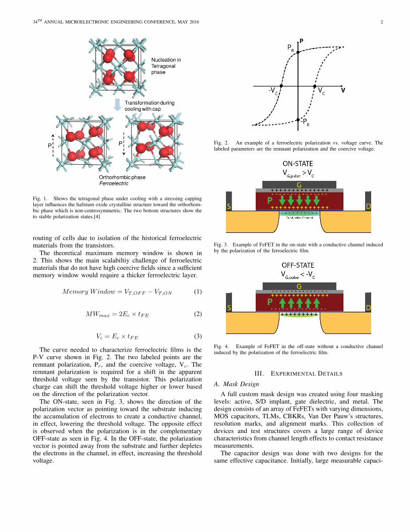
The ability to use an HfO2 based film for a ferroelectriclayer is hugely beneficial for integration into standard CMOSdue to the maturity of HfO2 as a high-k dielectric in modernprocess technology. Hafnium oxide has standard bulk and thinfilm crystalline phases which do not have ferroelectric proper-ties because the structure is centrosymmetric. However, duringcooling, thin layers of cation doped HfO2 under physical stressfrom a capping layer have been shown to have ferroelectricproperties in the resulting orthorhombic non-centrosymmetriccrystalline phase [4]. Fig. 1 shows the crystalline transitionsrequired to form ferroelectric hafnium oxide. Since the anneal-ing conditions are critical to inducing the ferroelectric phase,processing once the HfO2 has been annealed should be kept toa low thermal budget. NaMLab in Dresden, Germany providedthe atomic layer deposited (ALD) Si:HfO2 film, TiN cappinglayer, and anneal process for this work.
B. FeFET Device and OperationA FeFET device can be used as a memory device since the
polarization state of the ferroelectric film is stored and retainsthe state after power is removed. The use of the ferroelectricfilm as the dielectric reduces the complexity of the storagescheme to a 1T design. This reduces the area of the storage cellfrom the current FeRAM design with an access transistor and aferroelectric capacitor (1T-1C design). The compatibility withCMOS processing from hafnium based films also reduces the
34TH ANNUAL MICROELECTRONIC ENGINEERING CONFERENCE, MAY 2016 2
Fig. 1. Shows the tetragonal phase under cooling with a stressing cappinglayer influences the hafnium oxide crystalline structure toward the orthorhom-bic phase which is non-centrosymmetric. The two bottom structures show theto stable polarization states.[4]
routing of cells due to isolation of the historical ferroelectricmaterials from the transistors.
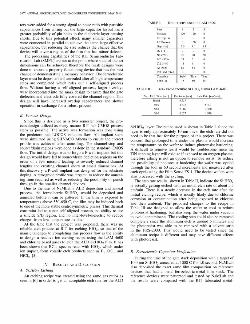
The theoretical maximum memory window is shown in2. This shows the main scalabiltiy challenge of ferroelectricmaterials that do not have high coercive fields since a sufficientmemory window would require a thicker ferroelectric layer.
Memory Window = VT,OFF − VT,ON (1)
MWmax = 2Ec × tFE (2)
Vc = Ec × tFE (3)
The curve needed to characterize ferroelectric films is theP-V curve shown in Fig. 2. The two labeled points are theremnant polarization, Pr, and the coercive voltage, Vc. Theremnant polarization is required for a shift in the apparentthreshold voltage seen by the transistor. This polarizationcharge can shift the threshold voltage higher or lower basedon the direction of the polarization vector.
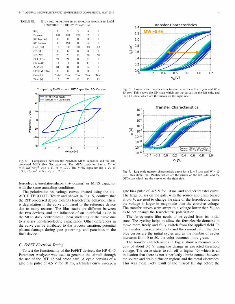
The ON-state, seen in Fig. 3, shows the direction of thepolarization vector as pointing toward the substrate inducingthe accumulation of electrons to create a conductive channel,in effect, lowering the threshold voltage. The opposite effectis observed when the polarization is in the complementaryOFF-state as seen in Fig. 4. In the OFF-state, the polarizationvector is pointed away from the substrate and further depletesthe electrons in the channel, in effect, increasing the thresholdvoltage.
Fig. 2. An example of a ferroelectric polarization vs. voltage curve. Thelabeled parameters are the remnant polarization and the coercive voltage.
Fig. 3. Example of FeFET in the on-state with a conductive channel inducedby the polarization of the ferroelectric film.
Fig. 4. Example of FeFET in the off-state without a conductive channelinduced by the polarization of the ferroelectric film.
III. EXPERIMENTAL DETAILS
A. Mask Design
A full custom mask design was created using four maskinglevels: active, S/D implant, gate dielectric, and metal. Thedesign consists of an array of FeFETs with varying dimensions,MOS capacitors, TLMs, CBKRs, Van Der Pauw’s structures,resolution marks, and alignment marks. This collection ofdevices and test structures covers a large range of devicecharacteristics from channel length effects to contact resistancemeasurements.
The capacitor design was done with two designs for thesame effective capacitance. Initially, large measurable capaci-
34TH ANNUAL MICROELECTRONIC ENGINEERING CONFERENCE, MAY 2016 3
tors were added for a strong signal to noise ratio with parasiticcapacitances from wiring but the large capacitor layout has agreater probability of pin holes in the dielectric layer causingshorts. Due to this potential effect, many smaller capacitorswere connected in parallel to achieve the same large effectivecapacitance, but reducing the size reduces the chance that thedevice will cover a region of the film that has minor defects.
The processing capabilities of the RIT Semiconductor Fab-rication Lab (SMFL) are not at the point where state-of-the-artdimensions can be achieved, therefore the mask designs weredone to ensure a properly functioning device that has the bestchance of demonstrating a memory behavior. The ferroelectriclayer must be deposited and annealed after all high temperaturesteps are completed which rules out a self-aligned processflow. Without having a self-aligned process, larger overlayswere incorporated into the mask design to ensure that the gatedielectric and electrode fully covered the channel region. Thisdesign will have increased overlap capacitances and sloweroperation in exchange for a robust process.
B. Process DesignSince this is designed as a two semester project, the pro-
cess design utilized as many mature RIT sub-CMOS processsteps as possible. The active area formation was done usingthe predetermined LOCOS isolation flow. All implant stepswere simulated using SILVACO Athena to ensure the correctprofile was achieved after annealing. The channel-stop andsource/drain regions were done as done in the standard CMOSflow. The initial design was to forgo a P-well implant but thisdesign would have led to source/drain depletion regions on theorder of a few microns leading to severely reduced channellengths and creating channel shorts at small dimensions. Atthis discovery, a P-well implant was designed for the substratedoping. A retrograde profile was targeted to reduce the anneal-ing time required as well as reducing the possibility of punchthrough in the smaller channel devices.
Due to the use of NaMLab’s ALD deposition and annealprocess, the ferroelectric Si:HfO2 would be deposited andannealed before it can be pattered. If the film is exposed totemperatures above 550-650 C, the film may be induced backto one of the more stable centrosymmetric phases. This thermalconstraint led to a non-self-aligned process, no ability to usea silicide S/D region, and no inter-level-dielectric to reducecharges from low-temperature oxides.
At the time that the project was proposed, there was noreliable etch process at RIT for etching HfO2, so one of themain challenges to completing this process flow is the abilityto design a reactive ion etching recipe using the LAM 4600and chlorine based gases to etch the ALD Si:HfO2 film. It hasbeen shown that BCln species react with HfO2, which underion impact, form volatile etch products such as BmOCln andHfCln [5].
IV. RESULTS AND DISCUSSION
A. Si:HfO2 EtchingAn etching recipe was created using the same gas ratios as
seen in [6] in order to get an acceptable etch rate for the ALD
TABLE I. ETCH RECIPE USED IN LAM 4600.
Step 1 2 3Pressure 120 120 0RF Top [W] 0 0 0RF Bottom 0 150 0Gap [cm] 3.0 3.0 5.3
O2 (111) 0 0 0N2 (222) 20 20 50BCl (333) 21 21 0Cl2 (444) 11 11 0Ar (555) 84 84 0CFORM (666) 0 0 0
Complete Stabl Time TimeTime [s] 15 60 15
TABLE II. DATA FROM ETCHING SI:HFO2 USING LAM 4600.
Step Etch Time [sec] Thickness [nm] Etch Rate [nm/min]
Initial 9.73760.0 4.337 5.40160.0 2.006 2.33060.0 0.027 1.979
Si:HfO2 layer. The recipe used is shown in Table I. Since thelayer is only approximately 10 nm thick, the etch rate did notneed to be that fast for the purpose of this project. There wasconcern that prolonged time under the plasma would increasethe temperature on the wafer to induce photoresist hardening.A difficult to remove resist would be troublesome since theTiN capping layer will oxidize if exposed to an oxygen plasma,therefore ashing is not an option to remove resist. To reducethe possibility of photoresist hardening the wafer was cycledthrough the tool in 60 second increments and measured aftereach cycle using the Film Sense FS-1. The device wafers werealso processed with the cycling.
The etch rate results, shown in Table II, indicate the Si:HfO2
is actually getting etched with an initial etch rate of about 5.5nm/min. There is a steady decrease in the etch rate after theinitial etching recipe, which is mostly likely due to chlorinecorrosion or contamination after being exposed to chlorineand then ambient. The proposed changes to the recipe inTable III are designed to allow the wafer to cool to reducephotoresist hardening, but also keep the wafer under vacuumto avoid contaminants. The cooling step could also be removedcompletely since the aluminum etch is around 5 minutes andthe photoresist was able to be removed with a solvent stripin the PRS-2000. This would need to be tested since thealuminum recipe is different and may have different effectswith photoresist.
B. Ferroelectric Capacitor Verification
During the time of the gate stack deposition with a target of10.0 nm Si:HfO2 annealed at 1000 C for 1.0 second, NaMLabalso deposited the exact same film composition on referencedevices that had a metal-ferroelectric-metal film stack. Thereference devices were patterned and tested by NaMLab andthe results were compared with the RIT fabricated metal-
34TH ANNUAL MICROELECTRONIC ENGINEERING CONFERENCE, MAY 2016 4
TABLE III. ETCH RECIPE PROPOSED TO IMPROVE PROCESS IN LAM4600 THROUGH DELAY IN VACUUM.
Step 1 2 3 4 5Pressure 120 120 120 120 0RF Top [W] 0 0 0 0 0RF Bottom 0 150 0 150 0Gap [cm] 3.0 3.0 3.0 3.0 5.3
O2 (111) 0 0 0 0 0N2 (222) 20 20 50 20 50BCl (333) 21 21 0 21 0Cl2 (444) 11 11 0 11 0Ar (555) 84 84 0 84 0CFORM (666) 0 0 0 0 0
Complete Stabl Time Time Time TimeTime [s] 15 75 60 75 15
Fig. 5. Comparison between the NaMLab MFM capacitor and the RITprocessed MFIS (N+ Si) capacitor. The MFM capacitor has a Pr of±15.2µC/cm2 with a Vc of ±1.2V . The MFIS capacitor has a Pr of±9.4µC/cm2 with a Vc of ±2.6V .
ferroelectric-insulator-silicon (n+ doping) or MFIS capacitorwith the same annealing conditions.
The polarization vs. voltage curves created using the aix-ACCT TF1000 FE Tester and shown in Fig. 5, confirm thatthe RIT processed device exhibits ferroelectric behavior. Thereis degradation in the curve compared to the reference devicedue to many reasons. The film stacks are different betweenthe two devices, and the influence of an interfacial oxide inthe MFIS stack contributes a linear stretching of the curve dueto a series non-ferroelectric capacitance. Other differences inthe curve can be attributed to the process variation, potentialplasma damage during gate patterning, and parasitics in thefinal device.
C. FeFET Electrical Testing
To test the functionality of the FeFET devices, the HP 4145Parameter Analyzer was used to generate the stimuli throughthe use of the RIT 12 pad probe card. A cycle consists of agate bias pulse of 4.5 V for 10 ms, a transfer curve sweep, a
Fig. 6. Linear scale transfer characteristic curve for a L = 5 µm and W =15 µm. This shows the ON-state which are the curves on the left side, andthe OFF-state which are the curves on the right side.
Fig. 7. Log scale transfer characteristic curve for a L = 5 µm and W = 15µm. This shows the ON-state which are the curves on the left side, and theOFF-state which are the curves on the right side.
gate bias pulse of -4.5 V for 10 ms, and another transfer curve.The large pulses on the gate, with the source and drain biasedat 0.0 V, are used to change the state of the ferroelectric sincethe voltage is larger in magnitude than the coercive voltage.The transfer curves were swept to a voltage lower than VC soas to not change the ferroelectric polarization.
The ferroelectric film needs to be cycled from its initialstate. The cycling helps to allow the ferroelectric domains tomove more freely and fully switch from the applied field. Inthe transfer characteristic plots and the current ratio, the darkblue curves are the initial cycles and as the number of cyclesincreases from 0 to 50, the color becomes more green.
The transfer characteristics in Fig. 6 show a memory win-dow of about 0.6 V using the change in extracted thresholdvoltage. The curve starts to roll off at higher VG which is anindication that there is not a perfectly ohmic contact betweenthe source and drain diffusion regions and the metal electrodes.This was most likely result of the missed HF dip before the

34TH ANNUAL MICROELECTRONIC ENGINEERING CONFERENCE, MAY 2016 5
Fig. 8. Threshold voltage change between the ON and OFF state for a L =5 µm and W = 15 µm. This shows a memory window, or change in VT tobe 0.6 V.
aluminum sputter deposition which left a thin oxide at theinterface between the electrode and diffusion region.
The sub-threshold characteristics are shown in Fig. 7 witha log scale. For both the ON-state and the OFF-state, thesub-threshold swing is around 110 mV/dec. This consistencybetween the two states allows for a large range of gate voltagesthat still have a 0.6 V memory window. It is not uncommon forthe different states of the device to have different sub-thresholdswings which would make the memory window inconsistent.The small changes in the drain current in the OFF-state curveis thought to be due to partial switching of the ferroelectricdomains during the sweep.
The change in the threshold voltage between the two states,or the MW, was consistent over the first 50 cycles at 0.6 Vshown in Fig. 8. The cycling at the beginning starts to open thememory window (MW) wider from 0.4 V to 0.6 V within 10cycles. This shows that with a 4.5 V stress for 10 ms, the deviceis ready quickly. There may be some reduction in cyclingstabilization if the pulse to the gate is in the nanosecond range.Testing was done to observe the minimum gate pulse widthrequired to achieve a 0.6 V MW, but the testing setup waslimiting the integrity of the pulse from the pulse generator tothe actual gate electrode. The steady reduction in the thresholdvoltage with increasing cycles could be an indication of atrapping mechanism which is a known problem with HfO2
based devices [1].The ON-to-OFF current ration is shown in Fig. 9. This
ratio can be used to determine the optimal read setting forthe device. To sense the state of the device, a large differencebetween the ON and OFF current needs to be observed by thesensing mechanism for the memory array. The device showsa difference larger than three orders of magnitude for a largerange of gate voltages.
The ID vs. VDS curves shown in Fig. 10 exhibit punchthrough even though a retrograde substrate well profile wasimplemented. Punch through is more apparent at lower gatevoltages since the gate has less control over the channel and thesource and drain depletion regions are larger. As you increase
Fig. 9. The ON to OFF current ratio is plotted vs. gate voltage to get anidea of the optimal read voltage. This device is a L = 5 µm and W = 15 µm.
Fig. 10. The ID vs. VDS curves of a L = 20 µm and W = 15 µm device.The gate voltage ranges from 0.0 V to 2.25 V in steps of 0.25 V.
the gate voltage the punch through effect happens at high VDS
bias.
V. CONCLUSION
The process that was developed at RIT was successful indemonstrating a functioning n-channel FeFET for use as amemory device with high compatibility with CMOS tech-nology using Si:HfO2. The ALD Si:HfO2 etch recipe wasdeveloped using chlorine based gases in the LAM 4600 RIE foran etch rate of 5.4 nm/min. The MFIS capacitors demonstratedferroelectric behavior similar to the MFM capacitors fromNaMLab which confirms the reasoning behind the thresholdvoltage shift when testing the FeFET device. There was a largecontact resistance due to imperfect processing that could beimproved on through silicide source and drains potentially. TheFeFET demonstrated a memory window of 0.6 V which wasindependent of the transistor dimensions as it is a charge effectand the polarization charge is measured per unit area.

34TH ANNUAL MICROELECTRONIC ENGINEERING CONFERENCE, MAY 2016 6
ACKNOWLEDGMENT
The author would like to thank Dr. Uwe Shroeder andClaudia Richter of NaMLab in Dresden, Germany becausewithout their support this project would not have been possible.Thanks to Dr. Santosh Kurinec and Jackson Anderson for theirimmense help and input throughout the project. He would alsolike to thank Dr. Robert Pearson, Dr. Dale Ewbank, Dr. LynnFuller, and Dr. Karl Hirschman for the processing and testingadvice. Many thanks to the entire SMFL staff for all of theirsupport and contributions.
This work was supported in part by the National ScienceFoundation, Grant # ECCS-1541090. Any opinions, findings,and conclusions or recommendations expressed in this materialare those of the author(s) and do not necessarily reflect theviews of the National Science Foundation
REFERENCES
[1] E. Yurchuk, Electrical Characterisation of Ferroelectric Field EffectTransistors based on Ferroelectric HfO2 Thin Films. Logos VerlagBerlin GmbH.
[2] J. Mller, E. Yurchuk, T. Schlsser, J. Paul, R. Hoffmann, S. Mller,D. Martin, S. Slesazeck, P. Polakowski, J. Sundqvist, M. Czernohorsky,K. Seidel, P. Kcher, R. Boschke, M. Trentzsch, K. Gebauer, U. Schrder,and T. Mikolajick, “Ferroelectricity in HfO2 enables nonvolatile datastorage in 28 nm HKMG,” in 2012 Symposium on VLSI Technology(VLSIT), pp. 25–26.
[3] K. M. Rabe, C. H. Ahn, and J.-M. Triscone, Physics of ferroelectrics :a modern perspective, ser. Topics in applied physics,. Springer.
[4] T. S. Bscke, J. Mller, D. Bruhaus, U. Schrder,and U. Bttger, “Ferroelectricity in hafnium oxide thinfilms,” vol. 99, no. 10, p. 102903. [Online]. Available:http://scitation.aip.org/content/aip/journal/apl/99/10/10.1063/1.3634052
[5] J. Shoeb and M. J. Kushner, “Mechanisms for plasma etchingof HfO2 gate stacks with si selectivity and photoresisttrimming,” vol. 27, no. 6, pp. 1289–1302. [Online]. Available:http://scitation.aip.org/content/avs/journal/jvsta/27/6/10.1116/1.3231480
[6] Y.-H. Joo, J.-C. Woo, X. Yang, and C.-I. Kim, “Temperaturedependence on dry etching of hafnium oxide using an inductivelycoupled plasma,” vol. 406, no. 1, pp. 176–184. [Online]. Available:http://dx.doi.org/10.1080/00150193.2010.484648
Joe McGlone received a B.S. in MicroelectronicEngineering from Rochester Institute of Technologyin May 2016. He will be pursuing his doctorate inElectrical Engineering from Ohio State Universitystarting in Fall 2016. He has completed three co-ops during his time at RIT, two at IBM in Fishkill,NY and one with AMD in Austin, TX. He has beenawarded a University Fellowship from Ohio StateUniversity as well as a three year Graduate ResearchFellowship from the National Science Foundation.