field emission – based many-valued processing using carbon
TRANSCRIPT

Multiple-Valued Computing Using Field Emission – Based Carbon Nanotube Controlled Switching
Anas N. Al-Rabadi and Marwan S. Mousa
Abstract - A new carbon nanotube (CNT) - based controlled switch is introduced. The new CNT device is a field emission – based device that uses field electron emission from the CNT to implement the functionality of controlled switching. To implement the field emission CNT controlled switch, four field emission CNTs that have single carbon nanotubes as the emitters were tested; two with single-walled CNT and two with multi-walled CNT. A tube with a tungsten tip was also used for comparison. The Fowler-Nordheim analysis of the DC current-voltage data provided reasonable values for the local fields at the emitters and the sizes of the emitters. It is also shown within the new implementation of the controlled switch that square-wave pulses from a single laser diode with 20 mW power and 658 nm wavelength which is focused on each emitter increased the emitted current by 5.2% with the CNT and 0.19% with the compared tungsten tip. The extension of the new device from the two-valued to the general m-valued case is introduced, and the implementation of multiple-valued Galois circuits and systems utilizing the new CNT field emission – based device is also shown. Since the controlled switch is a basic block in the design of modern digital systems, the new CNT device can have a wide range of applications in a wide variety of nano circuits. Index Terms - Carbon Nanotubes, Controlled Switching, Fault Tolerance, Fowler-Nordheim Analysis, Field Emission, Multiple-Valued Computing, Nanotechnology.
1. INTRODUCTION
The field of nanotechnology is a new interdisciplinary field of research that cuts across several fields of electronics, chemistry, physics and biology, that analyzes and synthesizes systems in the nano scale (10-9 m) such as nanoparticles, nanowires and carbon nanotubes (CNTs) [1-5,8,10,11,13,19,22,24]. The CNT technology is one of several cutting-edge emerging technologies within nanotechnology that is showing high efficiency and very wide range of applications in several various fields in science and technology [2-4,6-8,10,13,19,22,24,25,27,30,33]. Recent examples of such applications include: (1) TVs based on field-emission of CNTs that consume much less power, thinner and are of much higher resolution than the best plasma-based TVs available, and (2) nanocircuits based on CNTs such as CNT Field Effect Transistors that show big potentials for consuming less power and to be much faster than the available Silicon-based Field Effect Transistors. A. N. Al-Rabadi is with the Computer Engineering Department, The University of Jordan, Amman, Jordan (Phone: + 962-79-644-5364; E-mail: [email protected]; URL: http://web.pdx.edu/~psu21829/) M. S. Mousa is with the Physics Department, Mu’tah University, Al-Karak, Jordan (E-mail: [email protected])
The recently conducted simulations and experiments had shown that photomixing (i.e., optical heterodyning) in laser-assisted field emission could be used as a new microwave or terahertz (THz) source with a multi-octave bandwidth [8,9,20,23,26,27]. The field emitter tip used is much smaller than the wavelength of the incident optical radiation so quasi-static conditions require that the electric field of the radiation is superimposed on the applied static field to modulate the height of the energy barrier. In the conducted experiments, electrons usually tunnel from the tip into vacuum with a delay τ of less than 2 fs. Therefore, because the current-voltage characteristics of field emission are extremely nonlinear [6,12,25,30], it is shown that if two lasers are focused on the tip, the mixer current would follow each cycle of the difference frequency of the two lasers from DC up to 500 THz (which is equal to 1/τ). It is also shown that the tip will withstand applied static fields as high as 9 V/nm, so that incident laser radiation with comparable field strengths could produce a bright source of microwave or THz radiation. Carbon nanotubes are excellent field emitters [6-9,12,15,25,27,28,30] and facilitate the miniaturization of electronic devices [2,4,5,10,11,13,19,22]. Furthermore, the kinetic inductance of CNT causes them to be high impedance (approximately 5 kΩ) transmission lines, and had shown that this effect can be used for efficient broadband matching to the high impedance that is inherent in the field emission. This paper introduces a novel CNT field emission – based device that implements one fundamental building block in logic synthesis – the controlled switch [1,2,4,21,32], and the use of the new device in the general multiple-valued computations is also shown for the important case of ternary Galois logic (GF3). Figure 1 illustrates the layout of the introduced CNT-based system design methodology. Layer 1 shows the underlying utilized Galois field algebra. Layer 2 illustrates the field emission physics which is used in the operation of the new device. Layer 3 shows the technology of carbon nanotubes which is used in the synthesis of the new field emission – based device, and Layers 4-6 show the hierarchical implementation for applications within the system level. Although the multiple-valued implementation of the new CNT-based controlled switch is demonstrated in this work for the case of GF3, the implementations and extensions over higher radices of Galois logic and other algebras are similar.

System Applications Electronic Circuits Electrical Devices
Carbon Nanotube Technology Field-Emission Physics Galois Field Algebra
Figure 1. The introduced and utilized CNT-based implementation hierarchy. Basic background on CNTs is presented in Section 2. The description and static characterization of the CNT-based field emitters along with the required experimental measurements that characterize the time-dependent response of field emission by single carbon nanotubes are presented in Section 3. The new CNT field emission-based controlled switch is introduced in Section 4. The implementation of parity-preserving reversible controlled-swap gate using the new CNT-based controlled switch is introduced in Section 5. Several examples of multiple-valued computations using the new device are introduced in Section 6. Conclusion is presented in Section 7. 2. CARBON NANOTUBES Carbon nanotubes have attracted attention in recent years not only for their relatively small dimensions and unique morphologies, but also for their potential implementations in many current and emerging technologies [2-4,6-8,10,13,19,22,24,25,27,30,33]. The CNT is made from graphite [2,10,11,13,19,22,24]. It has been observed that graphite can be formed in nano-scale in three forms [5,10,11,19]: (1) Carbon Nanoball (CNB) (or buckyball) – molecule consisting of 60 carbon atoms (C60) that are arranged in the form of a soccer ball, (2) Carbon Nanotube (CNT) - narrow strip of tiny sheet of graphite that comes mainly in two types of (a) multi-wall CNT (MWCNT) where each CNT contains several hollow cylinders of carbon atoms nested inside each other and (b) single-wall CNT (SWCNT) that is made of just a single layer of carbon atoms, and (3) Carbon Nanocoil (CNC). The CNT, which is a cylindrical sheet of graphite, is formed geometrically in two distinct forms which affect CNT properties: (1) straight CNT in which a CNT is formed as a straight cut from graphite sheet and rolled into a carbon nanotube, and (2) twisted CNT in which a CNT is formed as a cut at an angle from graphite sheet and rolled into a carbon nanotube. Figure 2 shows a typical carbon nanoball (i.e., buckyball), SWCNT, and Scanning Electron Microscopy (SEM) image of chemical vapor deposition (CVD) grown array of MWCNT towers.
(a) (b) (c)
Figure 2. Various formations and shapes of CNTs: (a) carbon nanoball (i.e., buckyball), (b) single-wall CNT, and (c) an image from the Scanning Electron Microscopy (SEM) of chemical vapor deposition (CVD) grown array of multi-walled CNT towers. As previously mentioned, the newly emerging CNT technology has been implemented in many new promising applications [2-4,6-8,10,13,19,22,24,25,27,30,33]. These applications include (1) TVs that are based on the field emission of CNTs that consume much less power, thinner and have much higher resolution than the best plasma-based TVs available, (2) nano circuits based on CNTs such as CNT-based FETs that consume less power and are much faster than the available silicon-based FETs, (3) Carbon Nanocoils that can be used as inductors in nanofilters and as nanosprings in nano dynamic systems, and (4) CNT rings. The CNT has also potential exciting applications such as (1) CNT probes, (2) new composite materials, (3) CNT data storage devices capable of storing 1015 bytes/cm2, (4) drug delivery systems, (5) nano lithography, and (6) CNT gears in which larger gears drive smaller gears or vice versa. Figure 3 shows an important example of a CNT application in electronic systems as a channel in a Field Effect Transistor.
Figure 3. The use of the CNT as a channel in Field Effect Transistor-based devices. The CNT growth, as observed using (1) Transmission Electron Microscopy (TEM), (2) Atomic Force Microscopy (AFM) and (3) Scanning Electron Microscopy (SEM), requires processes with the correct conditions and materials. Currently, several methods for growing various types of CNTs exist [2,10,11,13,19,22,24]: (1) a big spark between two graphite rods, few millimeters apart, that are wired to a power supply in which a 102 Ampere spark between the two rods vaporizes carbon into hot plasma which partially re-condenses into the form of CNT, (2) chemical vapor deposition (CVD) of a hot gas such as methane in which a substrate is placed in an oven then the oven is heated to approximately 600 degrees Celsius and slowly methane is added; as methane decomposes, it frees carbon atoms that partially re-compose into the form of 0.6-1.2 nm in diameter SWCNTs, and (3) a laser blast of a graphite target in which

laser pulses blasts a graphite rod which generates hot carbon gas from which CNT forms. Although the CNT has been grown into several forms, CNT use is still limited as compared to other wide spread technologies. This is mainly due to: (1) it is still difficult to exactly control CNT growth into desired forms and (2) CNT growth is still very expensive due to the low yield of CNTs that meet the desired geometrical specifications. The existing and rapidly growing wide usability of CNTs in several applications is due to the unique structural properties they possess [2]. For example, the field emission property is used in the recently developed highly efficient CNT-based TV and is used in newly developed prototype vacuum tube lamps in six colors that are twice as bright as conventional light bulbs, longer-lived and at least ten times more energy-efficient. The properties of current carrying capacity, thermal stability, power consumption and electron scattering are qualifying the CNT for very promising future use in highly efficient power transmission. The property of preserving the electron spin will be utilized in using the CNT for reliable quantum-based computations [1]. The size property is very useful for using CNTs as nanowires that would result in decreasing the total size of areas and volumes that are occupied by wires and interconnects in the corresponding integrated circuits. The property of resilience is useful in building circuits and structures that has to maintain stress without structural damages. The CNT property of energy band gaps qualifies CNTs to be used in wide applications that require wide range of energy band gaps from the conductor state to the semiconductor state. 3. CARBON NANOTUBE - BASED FIELD EMITTERS This section presents important functional modeling of field emitters and the corresponding experimental setups and measurements that characterize the time-dependent response of CNT-based field emission [18] from which the operation of the new CNT field emission – based device will be demonstrated in Section 4. 3.1. Description and Static Characterization of the Field Emitters In order to perform the static modeling of CNT field emitters, four field emission carbon nanotubes, which are shown in Figures 4(b)-4(e), were manufactured by Xintek, Inc. [18]. The copper anode is at the right and the CNT emitter is mounted on a tungsten wire attached to the copper cylinder at the left as shown in Figure 4(a). Figures 4(b)-4(e) show the images of CNT emitters for each carbon nanotube, taken with a JEOL Ltd. model JEM 6300 SEM [18]. Carbon nanotubes M-1 and M-4 have a single MWCNT as the emitter, and carbon nanotubes C-3 and C-6 have a single SWCNT as the emitter. The used CNTs were formed in bundles that have diameters of 10-30 nm, but in each carbon
nanotube the field emission is from the one CNT at the end of the bundle where the electric field is most intense.
(a) (b) (c)
(d) (e)
Figure 4. Carbon nanotube – based field emission: (a) appearance of the field emission carbon nanotubes manufactured by Xintek, Inc. and (b) - (e) the Scanning Electron Microscopy (SEM) images of the CNT emitters in the four utilized carbon nanotubes. In the conducted imaging, the dimensions of the individual CNTs were not determined. The DC current-voltage characteristics were measured for these four carbon nanotubes, as well as a field emitter tube from Leybold Didactic GmbH, which has an etched single crystal of tungsten as the emitter [18]. All of the measurements that were made with the five tubes were performed at room temperature. The tungsten tip is mounted on a filament so that this tip is heated for cleaning shortly before each session of measurements. However, it is not possible to clean the CNT, which probably causes the “switch-on” effect in which the supply voltage must be momentarily increased well beyond the operating point to initiate field emission with the CNT. The data from the DC measurements were reduced by the Fowler-Nordheim analysis [14,18,29] which is based on the following simplified form of the Fowler-Nordheim equation that provides the magnitude of the current density as a function of the applied static field for the field emission from a specific material [14,16,29]:
J = A E2 e (-B/E) (1) where J and E are the magnitudes of the current density and the electric field intensity, A = 1.541 x 10⁻⁶/Φ, and B = 6.831 x 10⁹ Φ3/2. The work function Φ = 4.5 eV for tungsten, and for the CNT was set to Φ = 4.9 eV for graphene. In order to apply the Fowler-Nordheim equation to the DC current-voltage data, the following equation was also used which is valid for a given carbon nanotube, where I is the field emission current and V is the potential applied between the anode and the cathode:
I = CV2 e (-D/V) (2) Equations (1) and (2) can be combined to obtain the following equations for the parameters S and R, which are

used to characterize the field emitters:
S = CD2/AB2 (3) R ≡ V/E = D/B (4) where the parameter S refers to the effective emitting area which would be the physical area of the emitter if the current density were uniform over a fixed area and zero elsewhere, and the parameter R refers to the effective radius of curvature of the emitter but also includes the effects of local intensification of the electric field caused by elongation of the emitter or the reduction of the field which may be caused by shielding due to adjacent structures. The Fowler-Nordheim plots of the DC current-voltage data were conducted using ln(I/V2) as the ordinate and (1/V) as the abscissa [18]. Equation (2) requires that these plots should be straight lines and typically with correlation c ≈ - 0.998. Linear regressions based on these Fowler-Nordheim plots typically have a standard variance σ ≈ 0.08, and the probability for the null-hypothesis, that no linear relationship exists, is less than 0.0001. The values of the parameters C, D, S, R were determined from the linear regressions. A series ballast resistor of 100 MΩ was typically used in the measurements [18]. However, when the series ballast resistor was increased to 2.575 GΩ with carbon nanotube C-6, the obtained data were not consistent with the Fowler-Nordheim equation (c = - 0.846, σ = 0.738) even though the emitted current was stable at each value of the applied static potential. Figure 5 shows the anomalous data which were obtained using the 2.575 GΩ ballast resistor. In order to explain this effect, it is hypothesized that for currents greater than 500 nA, field emission with a single CNT may be intermittent, fluctuating at a high frequency. Thus, the average current, as measured by the DC microammeter, may be much greater with a large ballast resistor, and this is because at those times when the current is momentarily low, the voltage drop across the ballast resistor is at minimum so that high voltage occurs across the CNT, and this voltage causes a short-duration surge in the current.
0 .0 0 0 9 5 0 .0 0 1 0 0 0 .0 0 1 0 5 0 .0 0 1 1 0 0 .0 0 1 1 5 0
-3 2
-3 1
-3 0
-2 9
-2 8
-2 7
ln(I/
V2 )
1 /V
Figure 5. The obtained Fowler-Nordheim plot for CNT C-6 with 2.575 GΩ ballast resistor.
Several other conducted experiments have also observed the instabilities in the field emission from a single CNT [6,12,25]. However, the performed works didn’t describe the bias circuits which were used so it isn’t possible to determine if these instabilities were exacerbated by increasing the ballast resistor. Data which are consistent with the Fowler-Nordheim equation were obtained with carbon nanotube C-6 when the ballast resistor was decreased to values including 100 MΩ or 595 MΩ. The values of parameter R, the effective radius of curvature of the emitter, were found to vary within 77-110 nm for the four carbon nanotubes with CNT emitters. This suggests that values of the local electric field at the emitting sites were as high as 14 V/nm in some of these measurements. Others studying the field emission from various CNTs have provided approximate values for the electric field by dividing the applied voltage by the distance between the anode and the emitting tip, noting that this field would be intensified by the shape of the CNT, but not estimating the local electric field at the emitting sites. The Fowler-Nordheim analysis gave a value of 91 nm for the effective radius of curvature of the emitter in the Leybold tube [18], suggesting that the local electric field was as high as 5 V/nm in some of the performed measurements. Current densities as high as 109 and 1012 A/m2 may be drawn from a tungsten emitter in steady-state and pulsed operation, respectively, and the corresponding values of the applied static field are 4.7 and 8.6 V/nm which may be considered as limiting field strengths for tungsten under these conditions. Thus, the value of the parameter R which was obtained for the Leybold tube is reasonable. The Fowler-Nordheim analysis also showed that the parameter S, the effective emitting area, varied within 81-230 nm2 for the four carbon nanotubes with CNT emitters [18]. If the current density was uniform, this would correspond to circular emitting spots having radii of approximately 5-9 nm. Others have used Lorenz microscopy to directly observe the emitting sites for field emission from MWCNT and they found one or more sites having radii of several nm [15], and their data were in reasonable agreement with other performed experiments [7]. The Fowler-Nordheim analysis also showed that the effective emitting area for the tungsten tip in the Leybold tube would correspond to a hemisphere with a radius of 290 nm [18]. This result and the value of 91 nm for the effective radius of curvature of the emitter in the Leybold tube were in reasonable agreement with the radius of 100-200 nm which was specified by Leybold. 3.2. Experimental Measurements of the DC Current Variation which is Caused By a Laser Source While there is no means to couple microwave or terahertz power from any of the used five tubes, the step increase in the DC current that is caused by focusing a single square-wave modulated laser diode with the specifications of power
= 20 mW and wavelength = 658 nm on the field emission tip was measured [18]. The laser diode was maximally-focused to provide a measured Gaussian profile with a power flux density of approximately 107 W/m2 at the tip. The measured current step is equal to ½ of the peak value of the mixer current that would be generated if two stabilized tunable lasers each provided the same power flux density [18]. Thus, this low-frequency measurement can be used to estimate the mixer current which could be obtained by photomixing with these same field emitters. The laser diode was amplitude-modulated with a square-wave envelope and the field emission current was measured with a digital oscilloscope as shown in Figure 6. It was observed that the field emission tube itself behaves like a low-pass filter. The increase in the field emission current (I∆) acts as a current source, and it can be shown that when a square-wave current source is fed to a parallel R-C circuit, the voltage across the resistor has a saw-tooth waveform with a peak-to-peak value given by:
Vpp = R I∆ (1 – e -1/2τf) / (1 + e -1/2τf) (5) where I∆ is the peak-to-peak value of the current waveform and τ = RC. From Equation (5), one can show that Vpp0 ≡ Vpp (f = 0) = R I∆, and Vpp = R I∆/4τf = Vpp0 /4τf (for f >> 1/τ).
Figure 6. The used experiment for the conducted measurements with a square-wave modulated laser diode.
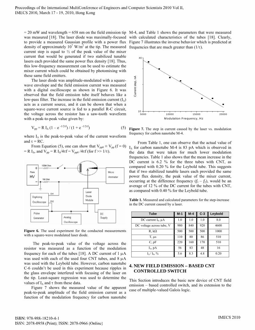
The peak-to-peak value of the voltage across the resistor was measured as a function of the modulation frequency for each of the tubes [18]. A DC current of 1 µA was used with each of the used four CNT tubes, and 8 µA was used with the Leybold tube. However, carbon nanotube C-6 couldn’t be used in this experiment because ripples in the glass envelope interfered with focusing of the laser on the tip. Least-square regression was used to determine the values of I∆ and τ from these data. Figure 7 shows the measured value of the apparent peak-to-peak amplitude of the field emission current as a function of the modulation frequency for carbon nanotube
M-4, and Table 1 shows the parameters that were measured with calculated characteristics of the tubes [18]. Clearly, Figure 7 illustrates the inverse behavior which is predicted at frequencies that are much greater than (1/τ).
5000 10000 15000 2000010
40
Cur
rent
ste
p, n
A
M odulation Frequency, Hz
Figure 7. The step in current caused by the laser vs. modulation frequency for carbon nanotube M-4.
From Table 1, one can observe that the actual value of I∆ for carbon nanotube M-4 is 83 pA which is observed in the data that were taken for much lower modulation frequencies. Table 1 also shows that the mean increase in the DC current is 6.2 % for the three tubes with CNT, as compared with 0.20 % for the Leybold tube. This suggests that if two stabilized tunable lasers each provided the same power flux density, the peak value of the mixer current, occurring at the difference frequency (f1 – f2), would be an average of 12 % of the DC current for the tubes with CNT, as compared with 0.40 % for the Leybold tube.
Table 1. Measured and calculated parameters for the step-increase in the DC current caused by a laser.
Tube M-1 M-4 C-3 Leybold
DC current I0, µA 1.0 1.0 1.0 8.0
DC voltage across tube, V 980 840 920 4600
R, kΩ 500 500 500 1000
Τ, µs 110 80 86 510 C, pF 220 160 170 510
I∆, pA 56 83 48 16
I∆ / I0, % 5.6 8.3 4.8 0.20
4. NEW FIELD EMISSION – BASED CNT CONTROLLED SWITCH This Section introduces the basic new device of CNT field emission – based controlled switch, and its extension to the case of multiple-valued Galois logic.

4.1. Two-to-One Controlled Switch Utilizing the previously experimented and observed CNT characterizations and operations from Section 3, Figure 8 introduces the new CNT field emission – based primitive that realizes the 2-to-1 controlled switch. In Figure 8, the input control signal that is used to control the electric conduct of the device is implemented using the imposed electric field intensity (E) or equivalently the work function (Φ) or voltage (V). (a) (b) (c) Figure 8. The CNT - based device implementing the operation of the 2-to-1 controlled switch: (a) the 2-to-1 logic multiplexer ( cbacG += ), (b) the CNT - based field emission – based 2-to-1 controlled switch, and (c) block diagram for the new 2-to-1 multiplexer. In this figure, HV is high-voltage source, VH is the complementary (i.e., opposite) high voltage source, and CS is the controlled switch. The description of the operation of the CNT field emission – based device shown in Figure 8(b) is as follows: by imposing the control signal of high voltage (HV), the voltage difference between the CNT cathodes and the facing anode is varied. This change will make the CNT cathode with control signal (HV) to be field emitting while the other CNT cathode with the complementary control signal ( VH ) to be without field emission. When the voltage difference is reversed, the CNT cathode with the complementary control signal ( VH ) will be field emitting while the other CNT cathode with the control signal (HV) will be without field emission. Thus, this device implements the functionality of the 2-to-1 controlled switch ( cbacG += ) which is shown in Figure 8(a). The experimental results show that the distance d required between the cathodes and the facing anode must be around 10 mm, or else beam distortion will occur affecting the collected current at the facing anode screen. Since the equations that relate the electric field intensity (E), work
(energy) function (Φ) in Joules (J), distance (d), voltage (V), and the current density (J), are as follows: Φ = e⋅V (6) V = E⋅d (7) d = V / E (8) J = I / (a/Ω) = I ⋅ (Ω/a) (9) where e is the electron charge ≅ 1.602 ⋅ 10-19 Coulombs (C), a is the tip area, and Ω is the emission angle, then the equation modeling the current value on the anode screen as related to Equations (1) and (6)-(9) is as follows:
2VVBd
e2Ωd
aAI⎟⎟⎟⎟
⎠
⎞
⎜⎜⎜⎜
⎝
⎛ −= (10)
From Equation (10), one can clearly observe the corresponding proportionality relation between the current value (I) and the voltage difference (V), proportionality relation between the current value (I) and the tip area (a), and the inverse relation between the current value (I) and the emission angle (Ω), where A = 1.541 x 10⁻⁶/Φ and B = 6.831 x 10⁹ Φ3/2. The values of the work function are Φ = 4.5 eV for tungsten and for CNT was set to Φ = 4.9 eV for graphene. The typical value used for the experiment input control variable of the electric field intensity (E) is ≥ 3⋅109 V/m, for the distance (d) between the CNT cathode and the facing anode screen is ≅ 10 mm, and V ≅ 3⋅107 V. 4.2. Many-to-One Controlled Switches Synthesizing many-to-one (i.e., m-to-1) CNT field emission – based controlled switches is possible using the fundamental two-to-one CNT field emission – based controlled switch from Figure 8(b). For example, for the 3-valued logic case, one needs two devices from Figure 8(b) to realize the functionality of three-to-one CNT field emission – based controlled switch. This idea is illustrated in Figure 9.
Figure 9. The 3-to-1 CNT field emission - based controlled switch, where the devices D1, D2 can be the CNT-based controlled switch device shown in Figure 8(b).
Control Signal #1: Condition #1 ≡ “0” Condition #2 ≡ “1”
Control Signal #2: Condition #1 ≡ “0” Condition #2 ≡ “1”
D1
D2
a b
c
2-1 CS
G
.
.
Control: c
Input1: a
Input2: b
G
R1
R2
HV HV - -

Note that, in Figure 9, device D1 outputs one signal from two input signals and device D2 outputs one signal from two input signals, thus the total functionality of the device in Figure 9 is a three-to-one CNT field emission – based controlled switch. In general, for an m-valued logic, one needs (m-1) of the 2-to-1 controlled switches to realize the function of an m-to-1 controlled switch. This is illustrated in Figure 10.
Figure 10. The realization of an m-to-1 controlled switch, where devices D1,..., D(m-1) can be the CNT field emission – based controlled switch from Figure 8(b). 5. THE IMPLEMENTATION OF PARITY- PRESERVING REVERSIBLE CONTROLLED- SWAP GATE USING THE NEW CNT FIELD EMISSION – BASED CONTROLLED SWITCH Due to the anticipated approaching failure of Moore’s law, quantum computing will play an increasingly important role in building more compact and less power consuming computers [1]. Due to this fact, and because all quantum computer gates (i.e., building blocks) should be reversible (i.e., information lossless) [1], reversible computing will have an increasingly more existence in the future design of regular, compact, and universal circuits and systems. Motivations for pursuing the possibility of implementing circuits and systems using reversible logic and quantum computing would include important design objectives such as power minimization, size miniaturization, speed maximization, and added error correction property [1]. For the error correction property, parity checking is one of the oldest and most widely used methods for error detection in digital systems. It is shown that reversible logic gates having an equal number of inputs and outputs are sufficient for the parity preservation if a reversible circuit at each gate is parity-preserving [1,17,31], where parity-preserving reversible logic gates refer to reversible gates for which the parity of the output matches that of the input, and the choice from such gates depends on the circuit design specifications in terms of the number of the used reversible gates, amount of needed “garbage” output which is used only for the purpose of ensuring reversibility, logical complexity, and the number of executed clock cycles.
Fredkin gate (which is also called the Controlled-Swap gate) [1] is one of the most fundamental building blocks in reversible and quantum computing, where many propositions have been performed to realize the Fredkin gate in various technologies such as optical, electrical, nano mechanical, and quantum [1-4]. The Fredkin gate belongs to a group of primitives where each represents a fundamental family of logic gates in reversible computing [1] that contain Fredkin-like, Toffoli-like, and Feynman-like gates [1], where the generalization of the fundamental Fredkin gate to an m-valued Galois logic was shown [1].
Control Signal #1: Condition #1 ≡ “0”
… Control Signal #(m-1):
Condition #1 ≡ “0” Condition #2 ≡ “1”
Condition #2 ≡ “1” In general, and as previously stated, the detection of
faults generated in a circuit can be performed using parity-preserving reversible logic gates. Given that reversible gates tend to have the same number of input and output vectors, a sufficient requirement for parity preservation in the course of reversible computation with such gates is that each gate should be parity-preserving, i.e., have the same parity for the input and output vector.
D1
D2 D3
. . .
. . .
. . .
D(m-1) The methodologies of implementations that are
developed is this section and in the following section are general and are applied in the m-valued Galois radix where m = pk, p is a prime number and k is a natural number of value k ≥ 1. Figure 11 shows the important examples of binary (i.e., second radix) and ternary (i.e., third radix) Galois field addition and multiplication tables.
(a) (b) (c) (d) Figure 11. Galois field addition and multiplication tables: (a) GF2(+), (b) GF2(*), (c) GF3(+), and (d) GF3(*). The following definition provides the formal specification for the two-valued parity-preserving reversible logic gate. Definition 1. For the binary radix of Galois field, let I = (a; b; c) and O = (P; Q; R) be the input and output vectors of a (3, 3) reversible gate, respectively. We call a reversible gate to be a Parity-Preserving Reversible Logic Gate (PPRLG) if the gate satisfies the parity-based equation: a ⊕ b ⊕ c = P ⊕ Q ⊕ R, where ⊕ is the Boolean Exclusive-OR (i.e., XOR) operation which is the GF2 addition operation. Figure 12 shows two commonly used PPRLGs [1] which are based on the fundamental Fredkin gate (also known as the two-valued reversible Shannon gate [1]). Both of the reversible gates in Figure 12 are clearly parity-preserving because both of them satisfy the parity-based equation which was shown in Definition 1.
+ 0 1 0 0 1 1 1 0
* 0 1 0 0 0 1 0 1
+ 0 1 2 0 0 1 2 1 1 2 0 2 2 0 1
* 0 1 2 0 0 0 0 1 0 1 2 2 0 2 1

While Definition 1 provides the formal specification of binary parity-preserving reversible gates, Definition 2 provides the formal specification of general m-valued parity-preserving reversible gates. Definition 2. A general m-valued Galois Parity-Preserving Reversible Logic Gate (PPRLG) satisfies the equation a +m b +m … +m c = P +m Q +m … +m R, where m = pk, p is a prime number, k is a natural number of value k ≥ 1, and a, b, …, c and P, Q, …, R are the corresponding input and output vectors of an m-valued (m + 1, m + 1) reversible gate, respectively. As an example of Definition 2, for the important specific case of the third radix Galois field, let I = (a; b; c; d) and O = (P; Q; R; L) be the input and output vectors of a ternary (4, 4) reversible gate, respectively. A ternary PPRLG is a gate that satisfies the parity-based GF3 equation of a +3 b +3 c +3 d = P +3 Q +3 R +3 L. For instance, Equation (11) characterizes the operation of the 3-valued Fredkin gate (also known as the 3-valued reversible Shannon gate) [1]:
(11) ⎥⎥⎥
⎦
⎤
⎢⎢⎢
⎣
⎡=
⎥⎥⎥
⎦
⎤
⎢⎢⎢
⎣
⎡
⎥⎥⎥
⎦
⎤
⎢⎢⎢
⎣
⎡
⎥⎥⎥
⎦
⎤
⎢⎢⎢
⎣
⎡
=
2
1
0
2
1
0
210
021
102
100010001
r
r
r
ggg
ggg
ccccccccc
gr
where ic is the 1-Reduced Post Literal which is a single variable function defined as ic = 1 if c = i else ic = 0 if c ≠ i where the variable c can take any value in the set 0,1,2 [1].
The corresponding gate that is represented by Equation (11) is reversible given that input c is produced in the output [1] for which a modified form of Equation (11) would be as shown in Equation (12):
(12) ⎥⎥⎥⎥
⎦
⎤
⎢⎢⎢⎢
⎣
⎡
=
⎥⎥⎥⎥
⎦
⎤
⎢⎢⎢⎢
⎣
⎡
⎥⎥⎥⎥
⎦
⎤
⎢⎢⎢⎢
⎣
⎡
⎥⎥⎥⎥⎥
⎦
⎤
⎢⎢⎢⎢⎢
⎣
⎡
=
cggg
cggg
ccccccccc
gr
r
r
2
1
0
2
1
0
210
021
102
1000010000100001
1000000
r
The reversible Shannon expansion in Equation (12) is represented using the 3-to-1 controlled switch as shown in Figure 13 [1]. Figure 13. Logic circuit realization of the reversible expansion in Equation (12). Table 2 illustrates the reversibility proof of the 4-input 4-output (i.e., (4, 4)) ternary Fredkin gate which is shown in Figure 13 and was formally represented by Equation (12).
g0 g1 c g1r0 g1r1 c 0 0 0 0 0 0 0 0 1 0 0 1 0 0 1 1 2 0 1 0 0 1 0 2 3 0 1 1 1 0 1 5 4 1 0 0 1 0 0 4 5 1 0 1 0 1 1 3 6 1 1 0 1 1 0 6 7 1 1 1 1 1 1 7
g0 g1 c g2r0 g2r1 c 0 0 0 0 0 0 0 0 1 0 0 1 0 0 1 1 2 0 1 0 1 0 0 4 3 0 1 1 0 1 1 3 4 1 0 0 0 1 0 2 5 1 0 1 1 0 1 5 6 1 1 0 1 1 0 6 7 1 1 1 1 1 1 7
0 1 2 0 1 2 0 1 2 c
gr0 gr1 gr2
g0 g1 g2
c
0 1 0 1
g0 g1
c c
g2r0 g2r1
0 1 0 1
g1r0 g1r1
c c
g0 g1
(a) (b) Figure 12. Representations for important reversible primitives: (a) reversible GF2 Shannon1 (i.e., Fredkin1) gate, and (b) reversible GF2 Shannon2 (i.e., Fredkin2) gate.

Both of the 2-to1 controlled switches in Figures 12(a) and 12(b) can be directly implemented using the CNT field emission - based realization that was shown in Figure 8(b), and the three 3-to-1 controlled switches in Figure 13 can be directly implemented using the 3-to-1 CNT field emission - based realization that was shown in Figure 9. 6. MULTIPLE-VALUED COMPUTING USING THE NEW CNT-BASED DEVICE Multiple-valued computing will be illustrated in this section using the new CNT field emission – based device that was developed in Section 4 for the case of ternary radix Galois field (GF3). Although the demonstration of the use of the new CNT-based controlled switch is for the case of GF3, implementations over higher radices of Galois logic follow the same proposed method. A controlled switch - based circuit that implements Figures 11(c) and 11(d) is shown in Figure 14, where Figure 14(a) can be implemented using the new 2-input single-output CNT field emission – based device from Figure 8(b). The internal nano interconnects in Figure 14(b) can be implemented using CNTs as well (cf. Figure 15), where = means a metallic CNT used as a nanowire, especially as the CNT possesses the important properties of small size, high resilience, and very low electron scattering.
Inputs (I) Outputs (O) g0 g1 g2 c gr0 gr1 gr2 c g0 g1 g2 0 g1 g2 g0 0 g0 g1 g2 1 g2 g0 g1 1 g0 g1 g2 2 g0 g1 g2 2
Table 2. The proof of the reversibility of the (4, 4) gate from Equation (12) and Figure 13.
I O I O I O I O I O I O I O I O I O
0000 0000 0100 1000 0200 2000 1000 0010 1100 1010 1200 2010 2000 0020 2100 1020 2200 2020
0001 0001 0101 0011 0201 0021 1001 0101 1101 0111 1201 0121 2001 0201 2101 0211 2201 0221
0002 0002 0102 0102 0202 0202 1002 1002 1102 1102 1202 1202 2002 2002 2102 2102 2202 2202
0010 0100 0110 1100 0210 2100 1010 0110 1110 1110 1210 2110 2010 0120 2110 1120 2210 2120
0011 1001 0111 1011 0211 1021 1011 1101 1111 1111 1211 1121 2011 1201 2111 1211 2211 1221
0012 0012 0112 0112 0212 0212 1012 1012 1112 1112 1212 1212 2012 2012 2112 2112 2212 2212
0020 0200 0120 1200 0220 2200 1020 0210 1120 1210 1220 2210 2020 0220 2120 1220 2220 2220
0021 2001 0121 2011 0221 2021 1021 2101 1121 2111 1221 2121 2021 2201 2121 2211 2221 2221
0022 0022 0122 0122 0222 0222 1022 1022 1122 1122 1222 1222 2022 2022 2122 2122 2222 2222
C
A 0
B 1
G
(a)
C0 C1 C2 C3
(b) Figure 14. The CNT - based implementation of Galois arithmetic operations: (a) controlled switch symbol that can be implemented using the CNT device in Figure 8(b), and (b) circuit that uses the controlled switch from Figure 14(a) to implement GF3 addition and multiplication tables from Figures 11(c) – 11(d).
A 0 B 1 0 1 2
0 1
0 1
0 1
K

Several efficient methods for implementing such interconnects have been reported by growing a SWCNT between two metal catalyst islands such as iron (Fe), cobalt (Co), nickel (Ni), yttrium (Y), or molybdenum (Mo).
(a) (b)
Figure 15. The implementation of CNT-based nano interconnects: (a) TEM image of a bundle of SWCNTs catalyzed by Ni/Y mixture, and (b) growing CNT wires on catalysts, where CNT meshes are shown on which the metal catalyst is coated. In Figure 14(b), the variables A, B are two ternary input variables that can take any value from the set 0, 1, 2, inputs 0, 1, 2 are constant inputs, and inputs Ck (k = 0, 1, 2, 3) are two-valued control variables that take values from the set 0, 1. Note that Figure 14(b) implements Figures 11(c) and 11(d) by using the appropriate values of control variables Ck that select the variable inputs A, B and constant inputs 0, 1, 2, where Table 3 shows an example for the implementation of Figures 11(c) and 11(d) using Figure 14(b). Table 3. An example for the implementation of Figures 11(c) - 11(d) using Figure 14(b), where + means GF3 addition from Figure 11(c), * means GF3 multiplication from Figure 11(d), Ck (+) means that the control variable Ck to implement the ternary addition operation, and Ck (*) means that the control variable Ck to implement the ternary multiplication operation.
Since m-valued circuits over GF3 will be synthesized using the addition and multiplication operations from Figures 11(c) and 11(d), the circuit in Figure 14(b) can be used in multiple-valued implementations whenever GF3 addition and multiplication operations are applied, and the internal nano interconnects can be implemented using metallic CNTs. A simple illustration is presented in the arithmetic circuit shown in Example 1.
Example 1. Let us implement the ternary function H = X4X1 +3 X2X3X1 +3 X2X3 using the addition and multiplication operations that are realized using Figure 14(b). X4
Figure 16. A GF3 circuit to implement the ternary function H = X4X1 +3 X2X3X1 +3 X2X3 using the two-input single-output operators from Figures 11(c) - 11(d), where Table 3 shows the implementation of Figures 11(c) - 11(d) using Figure 14(b) and = means a metallic CNT used as a nanowire. For instance, the corresponding GF3 addition and multiplication operations that are used in Figure 16 could be implemented using Table 3 (that specifies input values to Figure 14(b)) for specifying values to the various inputs. The following example demonstrates the system-level design of an Arithmetic and Logic Unit (ALU) circuit by illustrating the implementation of a 2-digit multiplier using the newly introduced CNT field emission - based device. Example 2. Let us design a ternary 2-digit multiplier. A 2-digit m-valued multiplication is performed utilizing the mod-multiplication operator as follows [1]:
B1 B0 A1 A0 Cout1 m01 m00 Cout2 m11 m10 0 Cout S3 S2 S1 S0 Figure 17 shows the general maps for the ternary multiplication and the output carry (Cout) functions, and Figure 18 shows the corresponding 3-valued circuit realization.
(a) (b) Figure 17. Ternary multiplication: (a) ternary multiply and (b) ternary carry out for the ternary 2-digit multiplier.
A B C G a b 0 a a b 1 b
A B C0
(+) C1
(+) C2
(+) C3
(+) C0
(*) C1
(*) C2
(*) C3
(*) + *
0 0 0 0 0 0 0 0 0 0 0 0 0 1 1 0 0 0 0 0 0 0 1 0 0 2 1 0 0 0 0 0 0 0 2 0 1 0 0 0 0 0 1 0 0 0 1 0 1 1 0 0 0 1 0 0 0 0 2 1 1 2 0 1 0 0 1 0 0 0 0 2 2 0 0 0 0 0 1 0 0 0 2 0 2 1 0 1 0 0 0 0 0 0 0 2 2 2 0 0 1 0 0 0 1 0 1 1
x y 0 1 2 0 0 0 0 1 0 0 0 2 0 0 1
x y 0 1 2 0 0 0 0 1 0 1 2 2 0 2 1
X2 X3 X1
X1
X2
X3 *
*
+
+ H * *

Figure 18. Logic circuit of a ternary 2-digit multiplier.
The corresponding GF3 addition and multiplication operations that are used in Figure 18 could be implemented using Table 3 that specifies input values to Figure 14(b) for specifying values to the various inputs. Further implementation of the general m-valued N-bit full ALU, which is the main functional unit in the microprocessor data path [1,21,32], that includes the realization of all arithmetic sub-units of addition, subtraction, multiplication and division, and includes the realization of all logic sub-units such as AND, OR and XOR, can be performed from the utilization of the new CNT-based controlled switch device that was introduced in Section 4 by using the same methodology which is used in the realization of the 2-digit multiplier shown in Figure 18.
7. CONCLUSION In this paper, a new carbon nanotube - based controlled switch is introduced. The realization of the new CNT field emission – based switching device is performed using four field emission tubes, having single CNT as the emitters, that were previously tested and a tube having a tungsten tip was used for the corresponding comparison. The Fowler-Nordheim analysis of the DC current-voltage data gave reasonable values for the local fields at the emitters and the sizes of the emitter sites. A single square-wave modulated laser diode of power (p) = 20 mW and wavelength (λ) = 658 nm focused on each emitter, increased the emitted current by an average of 6.2 % during each laser pulse with the CNT and 0.20 % with the tungsten tip. The measurements previously conducted with the CNT suggest that the mixer current could be 30 times greater if either SWCNT or MWCNT were used in place of the metal emitters, which would increase the microwave output power by 30 dB as a considerable improvement. While it was observed that, when
the laser beam is turned on, the field emission current increases with a characteristic time that is similar to the calculated thermal relaxation time of the field emitter (so this effect could be thermal), it was previously shown that the slow rise time for the current in such experiments is due to circuit effects. Also, electron pulses with durations of under 70 fs were recently generated by irradiating a field emitter with a low-power femtosecond laser, where it has been shown that this effect is non-thermal; the operating parameters may cause either photofield emission or optical field emission to be dominant. More pertinently, laser radiation was utilized to increase the field emission current from a cathode with a dense field of CNT by a factor of 18, and was shown that this is not a thermal effect by comparing the corresponding data with the effect of elevated temperatures on the field emission from the used CNT. The extension of the new two-valued CNT field emission – based device to the general m-valued case is introduced, and the general implementation of m-valued Galois circuits using the new CNT field emission – based controlled switching devices were also demonstrated. A 2-to-1 controlled switch is a basic building block in switch logic, where the concept of the switch logic is that logic circuits are implemented as combination of switches, rather than a combination of logic gates as in the gate logic, which proves to be less-costly in synthesizing wide variety of logic circuits and systems. Since the controlled switch is of fundamental importance in logic design, the new devices can have a wide spectrum of implementations in a wide variety of nano circuits where future work will investigate further speed and power analysis of the new devices and their related circuits and systems. REFERENCES [1] A. N. Al-Rabadi, Reversible Logic Synthesis: From Fundamentals to Quantum Computing, Springer-Verlag, 2004. [2] A. N. Al-Rabadi, “Carbon nano tube (CNT) multiplexers for multiple-valued computing,” Facta Universitatis – Electronics and Energetics, Vol. 20, No. 2, pp. 175 -186, 2007. [3] A. N. Al-Rabadi, “New dimensions in non-classical neural computing, Part II: quantum, nano, and optical,” International Journal of Intelligent Computing and Cybernetics, Emerald, Vol. 2, No. 3, pp. 513-573, 2009. [4] A. N. Al-Rabadi, Carbon NanoTube (CNT) Multiplexers, Circuits, and Actuators, United States Patent and Trademark Office, Patent No. US 7,508,039 B2, U.S.A., 24 March 2009. [5] G. Amaratunga, “Watching the nanotube,” IEEE Spectrum, pp. 28-32, 2003. [6] J.-M. Bonard, J.-P. Salvetat, T. Stöckli, L. Forro, and A. Chatelain, “Field emission from carbon nanotubes: perspectives for applications and clues to the emission mechanism,” Applied Physics A: Materials Science & Processing, 69(3):245-254, 1999. [7] J.-M. Bonard, K. A. Dean, B. F. Coll, and C. Klinke, “Field emission of individual carbon nanotubes in the scanning electron microscope,” Physical Review Letters, 89(19):197602-1:4, 2002.
0
*
+
B0 A0
+
B1 A0
0
++ + + 0
Cout S3 S2 S1 S0
+
B0 A1
+
B1 A1
0
* * *
[8] P. J. Burke, “Luttinger liquid theory as a model of the gigahertz electrical properties of carbon nanotubes,” IEEE Transactions on Nanotechnology, 1(3):129-144, 2002. [9] H.-F. Cheng, Y.-S. Hsieh, Y.-C. Chen, and I.-N. Lin, “Laser irradiation effect on electron field emission properties of carbon nanotubes,” Diamond and Related Materials, 13(4-8):1004-1007, 2004. [10] P. G. Collins and P. Avouris, “Nanotubes for electronics,” Scientific American, pp. 62-69, 2000. [11] P. G. Collins, M. S. Arnold, and P. Avouris, “Engineering carbon nanotubes and nanotube circuits using electrical breakdown,” Science, Vol. 292, 2001. [12] K. A. Dean and B. R. Chalamala, “Current saturation mechanisms in carbon nanotube field emitters,” Applied Physics Letters, 76(3):375-377, 2000. [13] V. Derycke, R. Martel, J. Appenzeller, and P. Avouris, “Carbon nanotube inter- and intramolecular logic gates,” Nano Letters, Vol. 0, No. 0, A - D, 2001. [14] R. H. Fowler and L. W. Nordheim, “Electron emission in intense electric fields,” Proceedings of the Royal Society A: Mathematical, Physical and Engineering Sciences, 119(781):137-181, 1928. [15] T. Fujieda, K. Hidaka, M. Hayashibara, T. Kamino, Y. Ose, H. Abe, T. Shimizu, and H. Tokumoto, “Direct observation of field emission sites in a single multiwalled carbon nanotube by Lorenz microscopy,” Japanese Journal of Applied Physics, 44(4A):1661-1664, 2005. [16] R. Gomer, “Field emission and field ionization,” American Vacuum Society classics, AIP, 1993. [17] M. Haghparast and K. Navi, “Design of a novel fault tolerant reversible full adder for nanotechnology based systems”, World Applied Sciences Journal, vol. 3, no.1, pp. 114-118, 2008. [18] M. J. Hagmann and M. S. Mousa, “Time-dependent response of field emission by single carbon nanotubes,” Jordan Journal of Physics, Vol. 1, No. 1, pp. 1-7, 2008. [19] J. R. Heath and M. A. Ratner, “Molecular electronics,” Physics Today, pp. 43-49, 2003. [20] P. Hommelhoff, Y. Sortais, A. Aghajani-Talesh, and M. A. Kasevich, “Field emission tip as a nanometer source of free electron femtosecond pulses,” Physical Review Letters, 96(7):077401-1:4, 2006. [21] R. C. Jaeger, Microelectronic Circuit Design, McGraw-Hill, New York, 1997. [22] J. Jiao, E. Einarsson, D. W. Tuggle, L. Love, J. Prado, and G. M. Coia, “High-yield synthesis of carbon coils on tungsten substrates and their behavior in the presence of an electric field,” Journal of Materials Research, Vol. 18, No. 11, pp. 2580-2587, 2003. [23] M. J. G. Lee and E. S. Robins, “Thermal relaxation of a laser illuminated field emitter,” Journal of Applied Physics, 65(4):1699-1706, 1989. [24] K. Likharev, “Hybrid semiconductor-molecular nanoelectronics,” The Industrial Physicist, pp. 20-23, 2003. [25] Y. Liu and S. Fan, “Field emission properties of carbon nanotubes grown on silicon nanowire arrays,” Solid State Communications, 133(2):131-134, 2005. [26] A. Mayer and J.-P. Vigneron, “Quantum-mechanical simulations of photon-stimulated field emission by transfer matrices and Green's functions,”Physical Review B, 62(23):16138-16145, 2000.
[27] A. Mayer, N. M. Miskovsky, and P. H. Cutler, “Photon- stimulated field emission from semiconducting (10, 0) and metallic (5, 5) carbon nanotubes,” Physical Review B, 65(19):195416-1:6, 2002. [28] A. Mayer, N. M. Miskovsky, and P. H. Cutler, “Three- dimensional simulations of field emission through an oscillating barrier from a (10, 0) carbon nanotube,” Journal of Vacuum Sci. & Tech. B, 21(1):395-399, 2003. [29] L. W. Nordheim, “The effect of the image force on the emission and reflexion of electrons by metals,” Proceedings of the Royal Society A: Mathematical, Physical and Engineering Sciences, 121(788):626-639, 1928. [30] A. N. Obraztsov, I. Pavlovsky, A. P. Volkov, E. D. Obraztsova, A. L. Chuvilin, and V. L. Kuznetsov, “Aligned carbon nanotube films for cold cathode applications,” Journal of Vacuum Science & Technology B, 18(2):1059-1063, 2000. [31] B. Parhami, “Fault-tolerant reversible circuits,” Proc. 40th Asilomar Conf. Signals, Systems and Computers, Pacific Grove, CA, pp. 1726-1729, 2006. [32] D. A. Patterson and J. L. Hennessy, Computer Organization and Design: The Hardware / Software Interface, Morgan-Kaufmann, 2008. [33] R. Tarkiainen, M. Ahlskog, J. Penttila, L. Roschier, P. Hakonen, M. Paalanen, and E. Sonin, “Multiwalled carbon nanotube: Luttinger versus Fermi liquid,” Physical Review B, 64(19):195412-1:4, 2001.