field emission performance of macroscopically gated...
TRANSCRIPT
The 30th International Electric Propulsion Conference, Florence, Italy
September 17-20, 2007
1
Field emission performance of macroscopically gated multiwalled carbon nanotubes for a spacecraft neutralizer
IEPC-2007-123
Presented at the 30th International Electric Propulsion Conference, Florence, Italy September 17-20, 2007
Karen L. Aplin* and Barry J. Kent.†
Rutherford Appleton Laboratory, Didcot, Oxfordshire, OX11 0QX, UK
Chris Castelli‡
Science and Technology Facilities Council, Swindon, Wiltshire, SN2 1SZ, UK
and
Wenhui Song§
Brunel University, Uxbridge, Middlesex, UB8 3PH, UK
Abstract: Field electron emission from aligned multiwalled carbon nanotubes has been assessed to determine if the performance, defined by power consumption, lifetime and emission currents, is suitable for use in spacecraft charge neutralization for field emission electric propulsion (FEEP). Carbon nanotubes grown by chemical vapor deposition were mounted on a dual in line chip with a macroscopic extractor electrode mounted ~1mm above the tubes. The nanotubes’ field emission characteristics (emission currents, electron losses and operating voltage) were measured at ~10-6 mbar. An endurance test of one sample, running at a software-controlled constant emission current lasted >1400 hours, approaching the longest known FEEP thruster lifetime. The emission corresponds to a current density of ~10 mAcm-2 at a voltage of 150V. These results, implementing mature extractor-electrode geometry, indicate that carbon nanotubes have considerable potential for development as robust, low-power, long-lived electron emitters for use in space.
Nomenclature CNT = carbon nanotube DIL = dual in line FEA = field emitter array FEEP = field emission electric propulsion i = current LISA = Laser Interferometer Space Antenna MWCNT = multi-walled carbon nanotube V = voltage
* Research Physicist, Space Science and Technology Department, [email protected] † Independent Consultant, Space Science and Technology Department, [email protected] ‡ Head of Space Science Group, Astronomy Division, [email protected]. § Research Lecturer, School of Engineering and Design, [email protected]

I. Introduction Field emission is a quantum tunneling effect under which electrons can be extracted from a material in a very
high electric field (typically ≥108Vm-1 [1]). Field emission devices are attractive electron sources for use in space because of their high current densities at low mass and power. The long lifetimes and repeatable characteristics required for deployment in space have already been demonstrated using arrays of high quality silicon tip field emitter arrays (FEA)2. Other field emission instrumentation is already in space, for instance, the Ptolemy mass spectrometer on the Rosetta mission (due to land on Comet Churyumov-Gerasimenko in 2014) uses field emission for ionization3. In this paper we evaluate the performance of carbon nanotubes (CNTs) as electron field emitters for spacecraft neutralizers to be used with micro-Newton electric propulsion.
A low power silicon field emission electron source to maintain spacecraft charge neutrality when used with field emission electric propulsion (FEEP) or colloidal thruster systems has already been constructed (it was originally intended for the Laser Interferometer Space Antenna (LISA) Pathfinder mission)4. It became clear that the number of processing steps required to produce Si FEAs to the required standards 5,6 places a significant cost, time and risk overhead on the manufacture. CNTs are attractive for neutralizer devices because they have low emission threshold potentials, high current densities, stable field emission over prolonged time periods, and are simpler to make than Si FEAs. A CNT neutralizer for a colloidal micro-Newton thruster already exists7, but it runs at 250-700V, and its power requirements would not be compatible with our baseline of 0.2WmA-1 defined by the LISA Pathfinder power supply subsystem8. Our principal motivation was therefore to investigate the possibility of using CNT for a low-power neutralizer, comparable to the silicon field emission neutralizer in performance.
The results presented use multi-walled CNT emitters produced by the pyrolysis of an organometallic precursor solution. This CNT geometry was selected because of its “forest” of aligned emitters (Figure 1). As field electron emission is principally a function of applied electric field, the CNT alignment optimises geometrical field enhancement, and reduces operating power. In the sections below, the production of a prototype CNT field emission chip is described followed by some basic tests to verify emission and lifetime. The endurance tests were performed at constant emission current, to emulate the planned FEEP neutralizer operation.
(b) (a)
Figure 1. Scanning electron micrographs of aligned multi-wall carbon nanotube film (a) plan view (b) top view.
II. Production and preparation of multi-walled carbon nanotubes The multi-wall carbon nanotubes (MWCNT) used for this study were synthesized using the thermal
decomposition of a hydrocarbon feedstock in the presence of an iron catalyst supplied as ferrocene dissolved in the liquid hydrocarbon (sylene, benzene or toluene). The tubes were grown on a flat silica substrate by a CVD method, injecting a solution of ferrocene (2 wt%) in toluene into a furnace at 760 °C under argon and hydrogen 9,10,11. This allows production of highly aligned MWCNT carpets (Figure 1), unlike most of the commercial MWCNT which are highly entangled. The product was characterised using a JEOL 6340F field emission gun scanning electron microscope (SEM) and a Renishaw 1000 micro-Raman spectrometer with a 514 nm excitation laser. For the growth conditions used, the average thickness of the CNT carpet is ~300 μm and the average diameter of the nanotubes is ~100 nm as measured by a scanning electron microscope. The MWNTs produced in this way are also at least 90% pure, with the major impurity being residual iron catalyst.
The free-standing MWCNT film was peeled off from the silica substrate and a 3 x 4 mm section was carefully (to preserve alignment of the nanotubes) transferred onto a dual in line (DIL) integrated circuit header using a thin
The 30th International Electric Propulsion Conference, Florence, Italy
September 17-20, 2007
2

The 30th International Electric Propulsion Conference, Florence, Italy
September 17-20, 2007
3
This mature geometry is ideal for space instrumentation, for whic
film of conductive epoxy. The DIL mount was chosen for compatibility with the existing test facility2, which was designed to test the Si FEAs5 used in the FEEP neutralizer4. For the Si neutralizer each DIL header contains 20 sample arrays, each designed to emit a nominal 6μA. (To make the neutralizer device, 66 of these 20-array die are wired together, to give a 6mA total current). This test facility has already been described in detail in the literature2 but will be briefly reprised in Section III. The Si FEAs previously tested were microfabricated with an integral gate electrode to which a voltage is applied to provide the electric field for emission. The CNT shown in Figure 1 do not include a gate electrode. Instead, a macroscopic extractor electrode was constructed by fixing a sheet of 1mm2 aperture, 74% transmission nickel mesh ~1mm above the CNT array with conducting epoxy, Figure 2. Two electrical connections were made: one to the base of the DIL header, and one to the mesh with copper wire. The use of an external mesh as the extractor (or gate) is similar to the approach taken in the first paper demonstrating field emission from CNT12 and, more recently, the “micro grid” used in [13]. h reliability and repeatability are more important
than novelty.
Nickel mesh
Silver loaded epoxy
III. Apparatus and Test Results The DIL header was installed in the field emitter test facility with the mesh connected to a Keithley 6487
picoammeter/voltage source, and the CNT electrically grounded via another Keithley 6487. A Faraday cup biased at 300V and placed ~2mm away from the mesh was used to detect the field emitted electrons, with currents measured using a third Keithley 6487. Results were logged to a PC through the IEEE-488 interface with control software written in the LabVIEW language. The extraction field is thus applied to the mesh, and any current ‘lost’ to the mesh is monitored, with the total current leaving the CNT measured by the picoammeter in the ground line. The only difference between this set-up and the arrangement for the silicon FEAs is that the mesh electrode, equivalent to the gate, is ~1mm away from the CNTs rather than ~1μm.
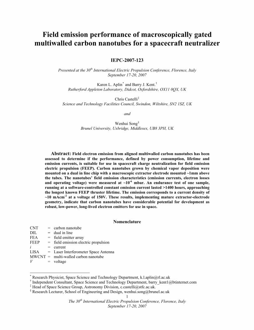
A. Basic Characterization Previous work with Si FEAs has indicated that a conditioning process is required to drive off any residual
impurities which may remain on the tip surface after the manufacture process1. Conditioning involves slowly increasing the extraction field to remove surface impurities by controlled emission. Conditioning is carried out carefully, as the different work functions of the impurity materials can give rise to rapidly varying emission properties. Once the impurities are removed, stable repeatable emission properties are observed and the emitters stay in that condition for the entire time that they remain under vacuum. Thus the CNTs for these measurements were also “conditioned” to remove surface impurities using a semi-automated process of slow (1 V/s) voltage increases and decreases, described in [2]. CNT field emission started at ~95V; typical current-voltage and Fowler-Nordheim responses (after conditioning) are plotted in Figure 3. Field emission physics (Fowler-Nordheim theory) predicts that field emission will cause a plot of ln(i/V2) against 1/V to be linear1, Figure 3b. This can be compared to Si FEAs, which started field emission at ~100V, corresponding to a minimum electric field of 108 Vm-1 (ignoring geometry-specific field enhancement, i.e. estimated by dividing 100V by the distance between the gate and the emitter, ~1μm). The CNTs however begin emission at an unenhanced field of <105 Vm-1 (i.e. 100V divided by 1mm). As this is too
DIL package
Conducting epoxy CNT Layer
DIL package
Electrical connection to nickel mesh
Electrical connection to CNT
Figure 2 Dual in line package (DIL) used for carbon nanotube (CNT) testing (a) Schematic showing the location of the nickel extractor mesh at a distance of ~1mm from the upper surface of the CNT layer (b) Photograph of the DIL package and external mesh,
low for field emission, which requires an electric field ≥108Vm-1 [1], field enhancement from the tube geometry must be substantial, at least 103. This is consistent with the CNT field enhancement expected in the literature14. The fraction of current lost to the mesh is greater than the maximum of 20% specified for the FEEP neutralizer, but this could be improved with a more careful choice of mesh (see Section IV B).
The 30th International Electric Propulsion Conference, Florence, Italy
September 17-20, 2007
4
B. Endurance Tests The endurance properties of the CNTs were tested by
running the tubes at a constant current of 12μA based on the conservative Si FEA spacecraft neutraliser specification2. The current was controlled in software by modulating the bias voltage to the mesh, with emission, mesh and Faraday cup collector currents all measured, as described above. Results are shown in Figure 4, with a mean current to the collector (Figure 4b) of 7.0±1.3 μA, (59% of the total emitted current). The average voltage required to generate this current is 164±19V (Figure 4d). The test was terminated after 1400 hours when the voltage was ~200V, which represents the upper voltage permitted by the software current controller, as defined by the spacecraft power supply limits for the Si FEA neutralizer. In this operating mode, deterioration in performance can be expressed in terms of either the voltage needed to obtain the desired current output, or by the change in the current losses to the mesh gate. There was no significant change in the current to the mesh over the test duration (Figure 4c), but the change in voltage was +0.05Vhr-1 (0.04%hr-1). This represents a substantial improvement in performance over the silicon FEAs tested2.
IV. Discussion
A. Lifetime This sample survived for >1400 hours, which is 70% of the
maximum lifetime demonstrated for any FEEP thruster, to the best of our knowledge15. In comparison, the optimized Si FEAs survived for 6000 hours only after much iteration in the fabrication process. It should also be noted that all the tests reported here were carried out on a single sample, and had a “fresh” sample been used for each phase of the testing the lifetime would undoubtedly have been longer.
0
2
4
6
8
10
12
14
16
18
80 100 120 140 160
Mesh voltage (V)
Cur
rent
( μA
)
Mesh currentEmitted currentCollector current
y = -1453.8x + 2.3995R2 = 0.9586
-20
-18
-16
-14
-12
-10
-8
-60.006 0.008 0.01 0.012 0.014 0.016
1/V
ln (i
/V2 )
(a)
(b)
Figure 3. (a) Current-voltage curve for a CNT array (b) Fowler-Nordheim plot for a CNT array.
B. Geometry The multi-wall tube geometry indicates a field enhancement of up to 103 in the samples tested. The estimated
current loss to the mesh extractor is approximately 50% of the emitter total; this is believed to be a consequence of the non-optimized design of the mesh gate-CNT geometry. An improvement in design might be to employ a thinner mesh, with smaller apertures and higher transmission. In addition, the CNT carpet used in this trial was not flat but was curved at the edges. Examination with an optical microscope suggested that most of the emission is from a small section of sample, ~0.13 mm2 which is closer to the mesh. Assuming all the emission is from this area, the emission current at constant voltage corresponds to a current density of ~10mAcm-2.

(a)
(b)
(c)
(d)
The 30th International Electric Propulsion Conference, Florence, Italy
September 17-20, 2007
5
The operating voltage and power consumption is coincidentally similar to the RAL field emitters, but is likely to be substantially reduced if the gate is closer to the CNT than the ~1mm on the prototype tested. CNT with integral gate electrodes, analogous to the Si FEAs do exist16, and perform at very low voltage; however the complex gate fabrication procedure increases the costs and risks inherent in production, similar to the Si FEA process, and therefore this seems undesirable for space applications until a greater level of technical maturity is reached. As the gated CNTs reported in [14] operate at ~10V, a simple assumption is that if the mesh gate electrode in the existing arrangement could be brought to <0.1mm from the CNT, similar performance could be expected as from the gated tubes with a much simplified production process. This could reduce the power consumption by an order of magnitude to ~15μWmA-1. This is likely to increase the lifetime of the neutralizer which is currently limited by array deterioration increasing the operating voltage to >200V; a lower operating voltage would give more room for drift upwards.
Figure 4 Time series showing (a) emitted current, (b) collected current, (c) losses to mesh and (d) mesh voltage during a test running at software-controlled constant emission current of 12μA.
C. Future Optimization These results based on tests carried out on a single sample are promising. Multiwalled, aligned, CNT have great
potential for development as low power field electron emitters for use in space. The applications are not limited to electric propulsion; an example of an additional application is the generation of X-rays for diffractometry. Further work will optimize the system, including an integral micromachined extractor electrode as an improvement on the existing Si FEA spacecraft neutralizer. The potential for performance improvements from better-controlled methods of CNT growth and positioning will also be investigated.
References 1I. Brodie and C. A. Spindt, “Vacuum microelectronics,” Adv. Electron. Electron Phys., 83, 1-105, 1992 2K. L. Aplin, C. M. Collingwood and B. J. Kent, “Reliability tests of gated silicon field emitters for use in space,” J. Phys. D.
App. Phys., 37, 14, 2009-2017, 2004 3B. J. Kent et al, “The use of microfabricated field emitter arrays in a high precision mass spectrometer for the Rosetta
mission”, Proc. 3rd Round Table on Micro/Nano Technologies for Space, European Space Agency, 2000 4B. J. Kent et al, “A field effect spacecraft neutraliser for the Lisa Pathfinder mission,” Class. Quantum Grav., 22, 10, S483-
S486, 2005 5L. Wang et al, “Optimisation of silicon FEAs fabrication for space application,” J. Vac. Sci. Tech. B., 22, 3, 1071-1023,
2004 6L. Wang et al, “Investigation of fabrication uniformity and emission reliability of silicon field emitters for use in space,” J.
Vac. Sci. Tech. B., 24, 2, 1056-1060, 2006

The 30th International Electric Propulsion Conference, Florence, Italy
September 17-20, 2007
6
7J. K. Ziemer et al, “Colloid Micro-Newton Thruster Development for the ST7-DRS and LISA Missions”, Proc. AIAA Joint Propulsion Conference and Exhibit, AIAA 2005-4265, 2005
8D. Nicolini et al, “μN propulsion subsystem developments for drag-free spacecraft”, Proc. Space Propulsion 2004, ESA SP-555, 2004
9R. Andrews et al, “Continuous production of aligned carbon nanotubes: a step closer to commercial realization,” Chem. Phys. Lett., 303, 467-474, 1999
10Z. J. Zhang et al, “Substrate-site selective growth of aligned carbon nanotubes,,” Appl. Phys. Lett., 77, 3764-3766, 2000 11C. Singh, M. S. P. Shaffer, and A. H. Windle, “Production of controlled architectures of aligned carbon nanotubes by an
injection chemical vapour deposition method,” Carbon, 41, 359, 2003 12W. A. de Heer, A. Chatelain and D. Ugarte, “A carbon nanotube field-emission electron source,” Science, 270, 1179, 1995 13W. Knapp and D. Schleussner, “Special features of electron sources with CNT field emitter and micro grid”, App. Surface
Sci. 251 (1-4), 164-169, 2005 14W. Zhu W., P. K. Baumann and C. A. Bower, “Novel cold cathode materials”, Vacuum Micro-electronics, edited by W.
Zhu, Wiley New York, 2001, pp 265-274 15A. Genovese et al, “Electric propulsion microthruster cluster,” J. Prop. Power 20, 2, 219-227, 2004 16G. Pirio et al, “Fabrication and electrical characteristics of carbon nanotube field emission microcathodes with an integrated
gate electrode”, Nanotechnology, 13, 1-4, 2002