field€emission€sem and low€voltage€sem - uni-ulm.de · obvious nonobvious facts about...
TRANSCRIPT

FIELD EMISSION SEMand
LOW VOLTAGE SEM
FT Unto TapperVTT Fine Particles
P.O.Box 100002044 VTT


Field Emission Scanning Electron Microscope
LEO DSMLEO DSM982 GEMINI982 GEMINIDigital Scanning Electron MicroscopeDigital Scanning Electron Microscope

Obvious nonobvious facts about electron microscopy
•We interpret our EM images using our experience from light optics.•For the best results the sample is the most important.•Instrument is not that important.

Motivation to buy a FEGSEM
Image obtained using
a normal SEM usingtungsten cathode.
MAG. x100k, HV 30kV.
We see in practice thestructure of sputtercoated Au/Pd.
Nucleporefilter
Agglomerated particles fromCoal fired boiler

Lens Aberrations
Astigmatism

Probe sizeSEM (&STEM) resolution is determined by the spot size
(on the sample)
The smallest diameter of the electron beam is determined by
1. The quality of the lens used for focusing
2. The performance of the electron gun (~ gun brightness )
= j0 /( 2), where j0 = current density (A/cm2) and = semiangle of beam convergence.
The beam size, d0, can be estimated by the relationship betweenthe total beam current and current density leading to d0:
1/ 2
0 1/ 2
2 p
p
Id
πα β= “High brightness small spot size”

Probe size
.4
,)(25.0)16.0(0
2222
2202
20
222
βαα
αλ p
cppsp
p
dcsp
ICwhere
EECCCd
ddddd
=∆
+++
=
⇒
+++=
Summing in quadrature (= assume gaussian shape) each of the aberration termswe have an estimate for the probe size:
Operator takes care of theastigmatism: X/Y stigmators
AND
the beam alignment along theoptical axis: Gun alignment(X/Y) and aperture alignment(X/Y).
Cs and Cc are instrument specific.However we can affect C0 bykeeping the tip in “good”condition and changing itregularly.

Field Emission Sources
•Cold Cathode (Cold FEG)
•Thermal Cathode (Thermal FEG)
•Shottky Emitter
In practice: Either cold FEG or Shottky Emitter

Electron sources
LaB6
Cold FEG
Tungsten

The present Shottky Emitter in our TEM

Comparison of various electron sources

DSM 982 GEMINIELECTRON OPTICS
Conventional column DSM 982 column

INLENS SEdetector andGemini lens
Lower or lateral on chamberSE detector
INLENS detector
Magnetic lens
Electrostatic lens

Lateral and inlens SE detectors give different informationINLENS = HIGH CONTRAST/ EFFICIENCY SE DETECTOR
Lateral detector InLens detector

New Zeiss Column
Cross section of an FESEM column with integrated beam booster and annular incolumndetectors: Uex — extractor voltage of first anode; Upe — primary beam voltage; UB —booster voltage; UF — EsB filtering grid voltage.
The integrated beam booster projects the SE (green) electrons on the annularSE inlens detector, and the BSE (blue) electrons are projected on theintegrated EsB detector.

Low Voltage performance
DSM 982 Gemini
resolution:
1 nm at 30 kV
1.2 nm at 20 kV
2.5 nm at 5 kV
4 nm at 1 kV
ULTRA 60&50
resolution:
1 nm at 15 kV
1.7 nm at 1 kV
4 nm at 0.1 kV
High voltage: 0.2 –30 kV High voltage: 0.1 –30 kV

SEMIINLENS AND CONVENTIONAL SEDETECTOR

LEO DSM982 GEMINIDigital Scanning Electron Microscope
•• AccelerationAcceleration voltagevoltage :: 0.2 kV0.2 kV 30 kV30 kV•• ElectronElectron SourceSource :: SchottkySchottky FEGFEG•• LensLens systemsystem :: aa uniqueunique design of adesign of a compoundcompound
5050°° conicalconical magneticmagnetic//electrostaticelectrostaticobjectiveobjective lenslens
•• ResolutionResolution :: 11 nmnm at 30 kV; 2.5at 30 kV; 2.5 nmnm at 5 kVat 5 kV•• DetectorsDetectors :: LateralLateral SESEdetectordetector
InInlenslens annularannular highhighcontrastcontrast SESEdetectordetectorBSEBSE detectordetectorNoran EDSNoran EDS microanalysermicroanalyser

Electron specimen interactions
Elastic Scattering
•Rutherford scattering (Coulombic interaction with atomic nucleus)
Inelastic scattering
•Phonon excitation (small lattice oscillations)
Typical temperature rice only few degrees Celcius but temperature rises of several hundred degrees Celsiusare possible.
•Plasmon Excitations
Waves in free electron gas in metallic species
•Secondary electron excitation
•Bremsstrahlung or continuum Xray emission
•Ionization of inner shell
Characteristic Xray emission, Auger electrons
In TEM we should also considerwhether the scattering is coherentor incoherent (HRTEM).

Beam interactions in the specimen

Upper crossover voltage for SE’s
At E2 number of beam electrons equals the number ofemitted secondary and backscattered electrons no netcurrent and no charging.

Depth of focus
0.2 mm,
where AP
DM
RWD
α
α
=
=
You can increase D by increasing the workingdistance or by decreasing the aperture size.

INTERACTION VOLUME AND VARIOUS ELECTRONINTERACTIONS
SE1: Best resolution, "single scattering"SE2: Multiple scatteringBSE: Backscattered electronsX: Xrays (bremstrahlung and characteristic)AE: Auger electrons
LVSEM:SE1 Yield increases,SE2 ja BSE less significant

Effect of high voltage on interaction volume
4 kV 12 kV
MonteCarlo simulation (10000 electrons): 100 nm TiO2on carbon.
0 nm356.4 nm 356.4 nm

Energy release in the sample
4 kV 12 kV

Effect of high voltage on SEI&SEII emission
For high resolution wehave two choices:
•Use low voltage
•Use high voltage andhigh magnification

Advantages of FEG SEM
•Better resolution.
•Possibility to work using low voltages (i.e. 0.2 –5 keV electronenergy).
•High brightness source ( = FEG):Fast imaging (TVrate, slowscan is not necessary).High countrates in Xray analysis.
•Easy to operate.

Advantages of Low Voltage SEM
•Analysis without conductive coating
•Decreased radiation damage
•Better topographic contrast
•Better surface sensitivity
•Better resolution (lateral and depth) in BSE/SE imaging
•Better resolution (lateral and depth) in Xray analysis

DSM 982 controls
Stigmators (X/Y)
Source (SE, SEinlens, BSE)
Magnification
(Coarse/Fine)
SE Brightness/ContrastManual/Auto
Scan controlTV, Slow Scan, variable raster,
spot mode
FocusCoarse/Fine
PositionX/Y fine shift
Focus wobble
Just for fun knob
Aperture (16, 3 = 6)
HV on/off HV selectioncoarse/fine
Filament current
Extractor voltage
Gun alignment
Aperture alignmentWorking distance
WD = Working distance
0.2 1kV: ~ 1 mm
1 –2 kV: max 7 mm
EDS intersection point: WD =13 mm
EDSBSE
detector
Objective lens
Inlens SE detector is switched ofat 20 kV.
This knob isnot fixed to
2 kV

Effect of high voltage in SE images
Specimen:
NanocrystallineTiO2particles collectedon holey carboncoated TEM grid.
Inlens SE detector
500 V 2 kV
5 kV 8 kV

Low Voltage BSE Imaging
Gold on carbon
TiO2particles
5 kV 5 kV
3 kV 3 kV
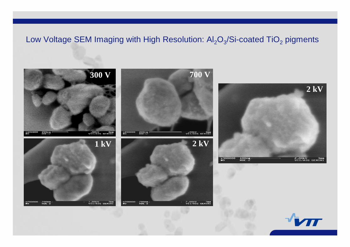
Low Voltage SEM Imaging with High Resolution: Al2O3/Sicoated TiO2 pigments
300 V 700 V
1 kV 2 kV
2 kV

Imaging with low voltage and high magnification (and hopefully withhigh resolution)
Surface structure of TiO2 pigmentsHV: 2 kV Mag: x400k
Mag: x200k
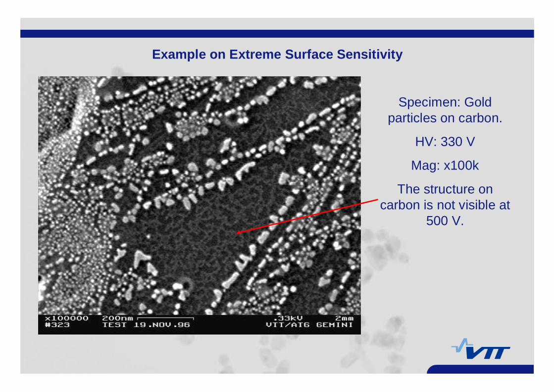
Example on Extreme Surface Sensitivity
Specimen: Goldparticles on carbon.
HV: 330 V
Mag: x100k
The structure oncarbon is not visible at
500 V.
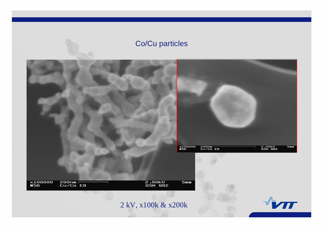
Co/Cu particles
2 kV, x100k & x200k

Sample definition and simulation parameters
300 nm ZrO
layer on Zr
substrate ZrZrZr
ZrOZrOZrO
Electron beam diameter: 3 nm (angle 900 with respect to samplesurface, Si(Li) Xray detector takeoff angle: 350)
Electron beam energy: 2, 5 and 8 keV
Number of simulated electrons: 10 000
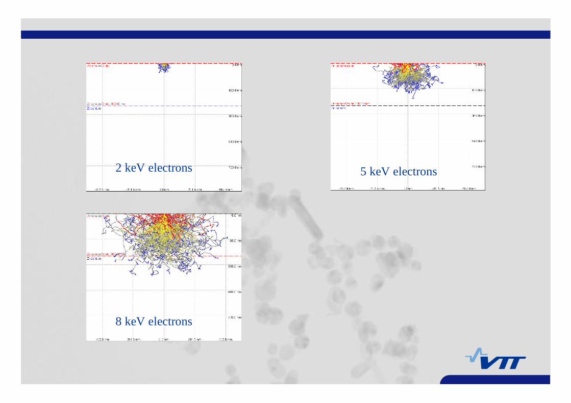
2 keV electrons 5 keV electrons
8 keV electrons

Elemental map for ZrO/Zr crosssectioned specimen (Zr, O, Sn)HV: 5 kV, Pixels: 128 x 128, Mag. x1000
Zr
Ir
O
CZr
SnO
