figure 9-1 block diagram of static ram table 9-1 truth table for
TRANSCRIPT
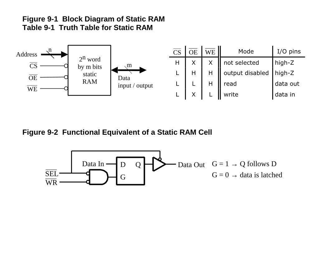
Figure 9-1 Block Diagram of Static RAMTable 9-1 Truth Table for Static RAM
Mode I/O pins
H X X not selected high-ZL H H output disabled high-Z
L L H read data out
L X L write data in
Figure 9-2 Functional Equivalent of a Static RAM Cell
2n wordby m bits
staticRAM
nAddress
CS
OE
WE
m
Datainput / output
CS OE WE
D
G
QData In
WRSEL
Data Out G = 1 → Q follows DG = 0 → data is latched
RowDecoder
A10
A 4
InputData
Control
I/O 7
I/O 0
Column Decoder
Column I/O
A3 A1A2 A0
Memory Matrix
128 X 128
OE
WE
CS
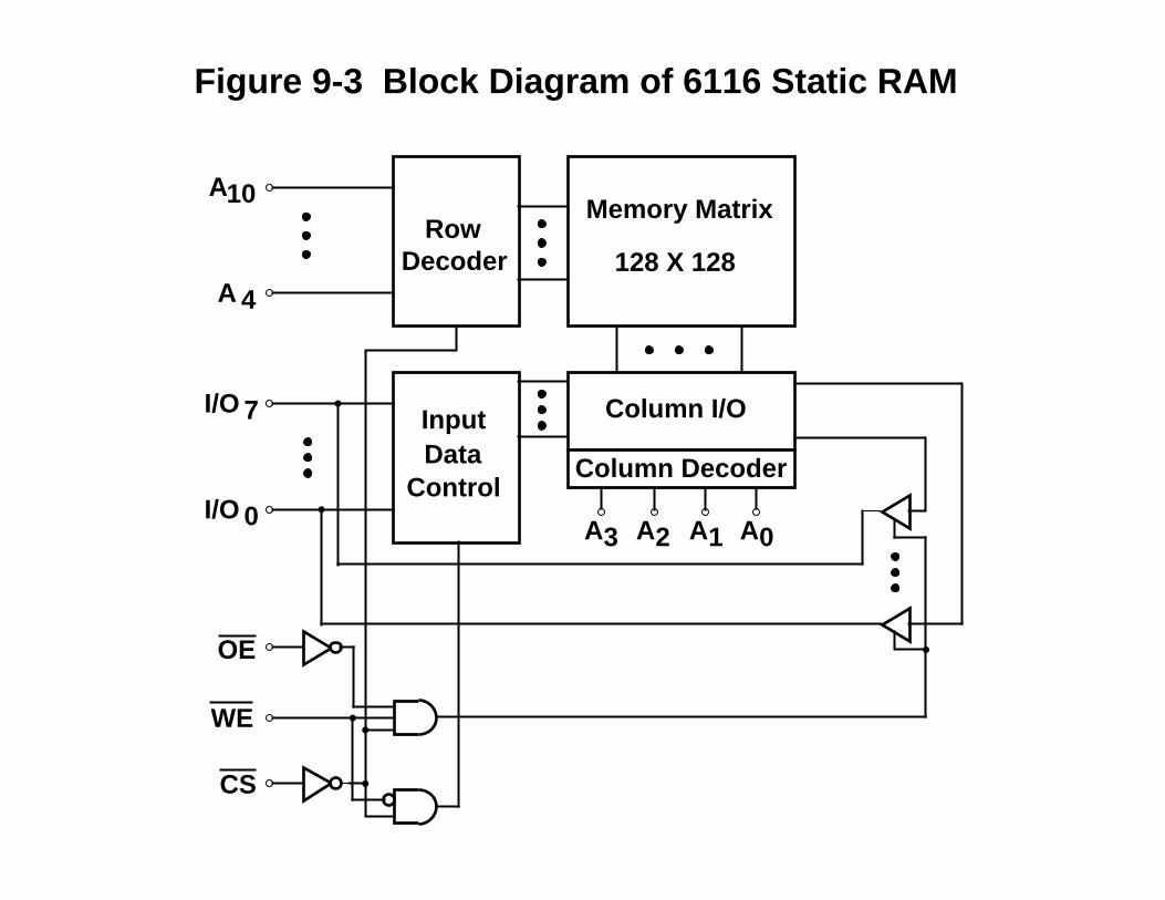
Figure 9-3 Block Diagram of 6116 Static RAM
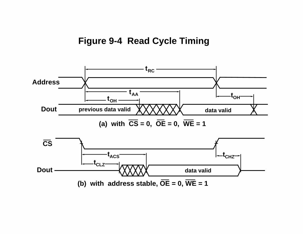
tOH
tAA
tRC
tOH
Address
Dout
CS
Dout
tCHZtACStCLZ
(a) with CS = 0, OE = 0, WE = 1
(b) with address stable, OE = 0, WE = 1
previous data valid data valid
data valid
Figure 9-4 Read Cycle Timing
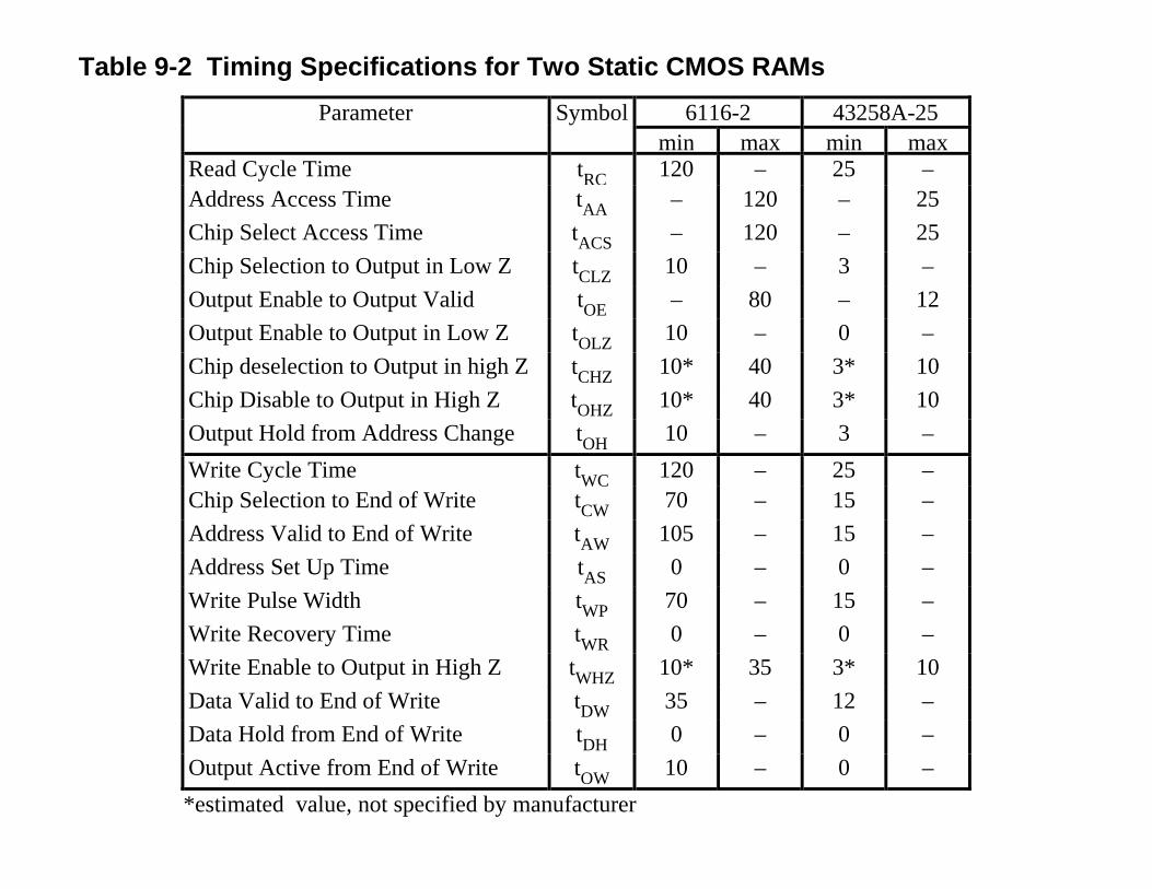
Table 9-2 Timing Specifications for Two Static CMOS RAMs
Parameter Symbol 6116-2 43258A-25min max min max
Read Cycle Time tRC 120 – 25 –Address Access Time tAA – 120 – 25Chip Select Access Time tACS – 120 – 25Chip Selection to Output in Low Z tCLZ 10 – 3 –Output Enable to Output Valid tOE – 80 – 12Output Enable to Output in Low Z tOLZ 10 – 0 –Chip deselection to Output in high Z tCHZ 10* 40 3* 10Chip Disable to Output in High Z tOHZ 10* 40 3* 10Output Hold from Address Change tOH 10 – 3 –
Write Cycle Time tWC 120 – 25 –Chip Selection to End of Write tCW 70 – 15 –Address Valid to End of Write tAW 105 – 15 –Address Set Up Time tAS 0 – 0 –Write Pulse Width tWP 70 – 15 –Write Recovery Time tWR 0 – 0 –Write Enable to Output in High Z tWHZ 10* 35 3* 10Data Valid to End of Write tDW 35 – 12 –Data Hold from End of Write tDH 0 – 0 –Output Active from End of Write tOW 10 – 0 –
*estimated value, not specified by manufacturer
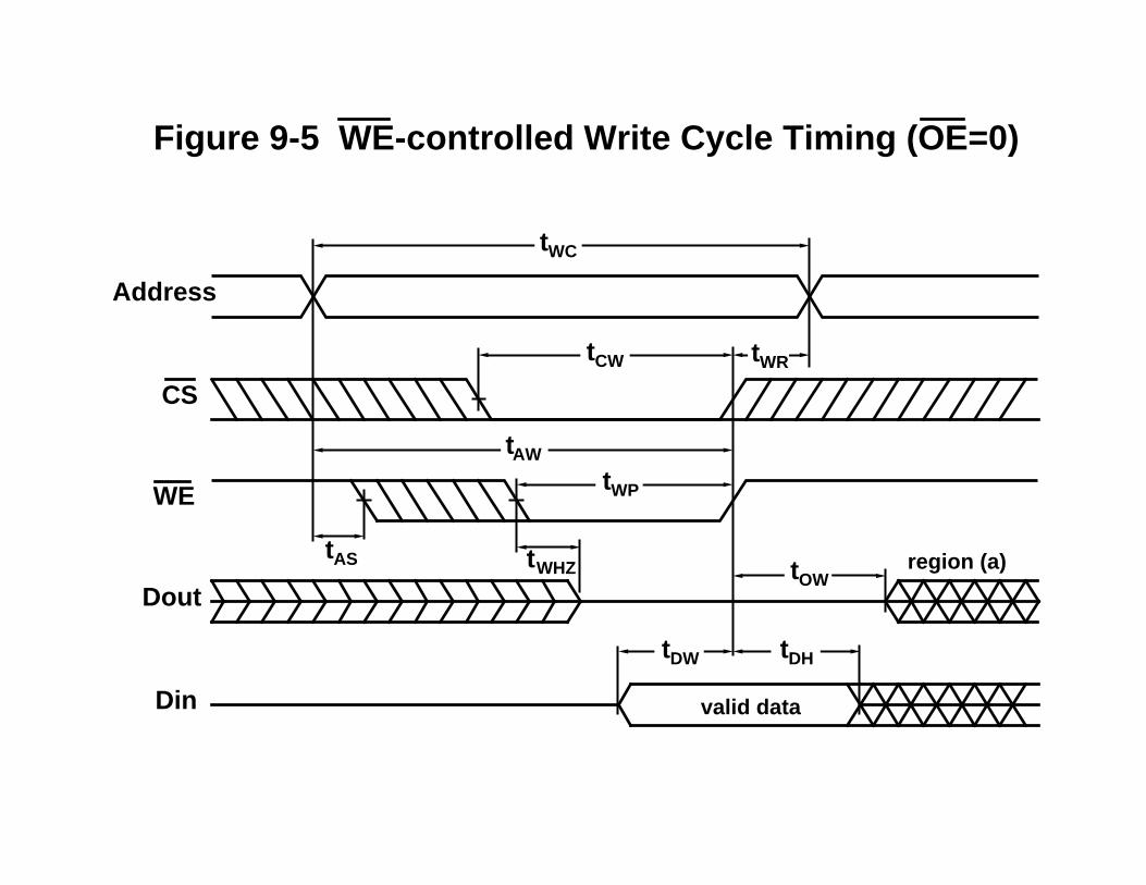
tAS
Address
CS
WE
Dout
Din
tWC
tCW tWR
tAW
tWP
tWHZ tOW
tDW tDH
valid data
region (a)
Figure 9-5 WE-controlled Write Cycle Timing (OE=0)
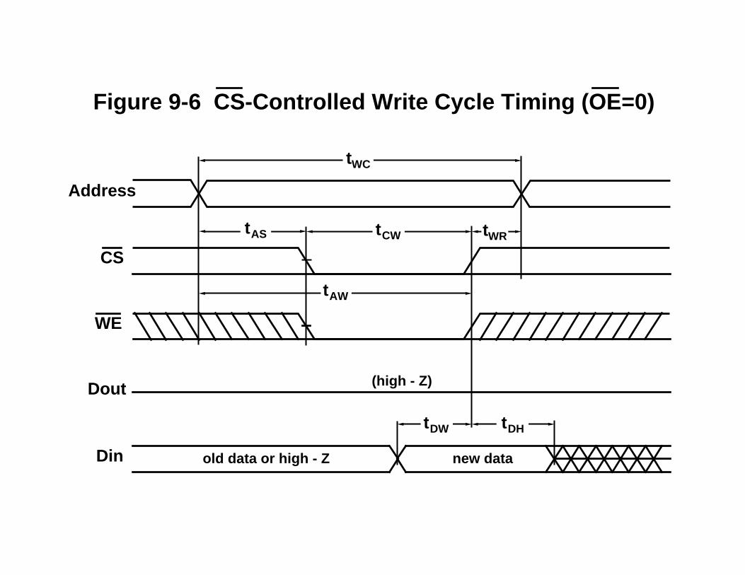
Address
CS
WE
Dout
Din
tWC
tCW tWR
tAW
tDW tDH
tAS
(high - Z)
old data or high - Z new data
Figure 9-6 CS-Controlled Write Cycle Timing (OE=0)
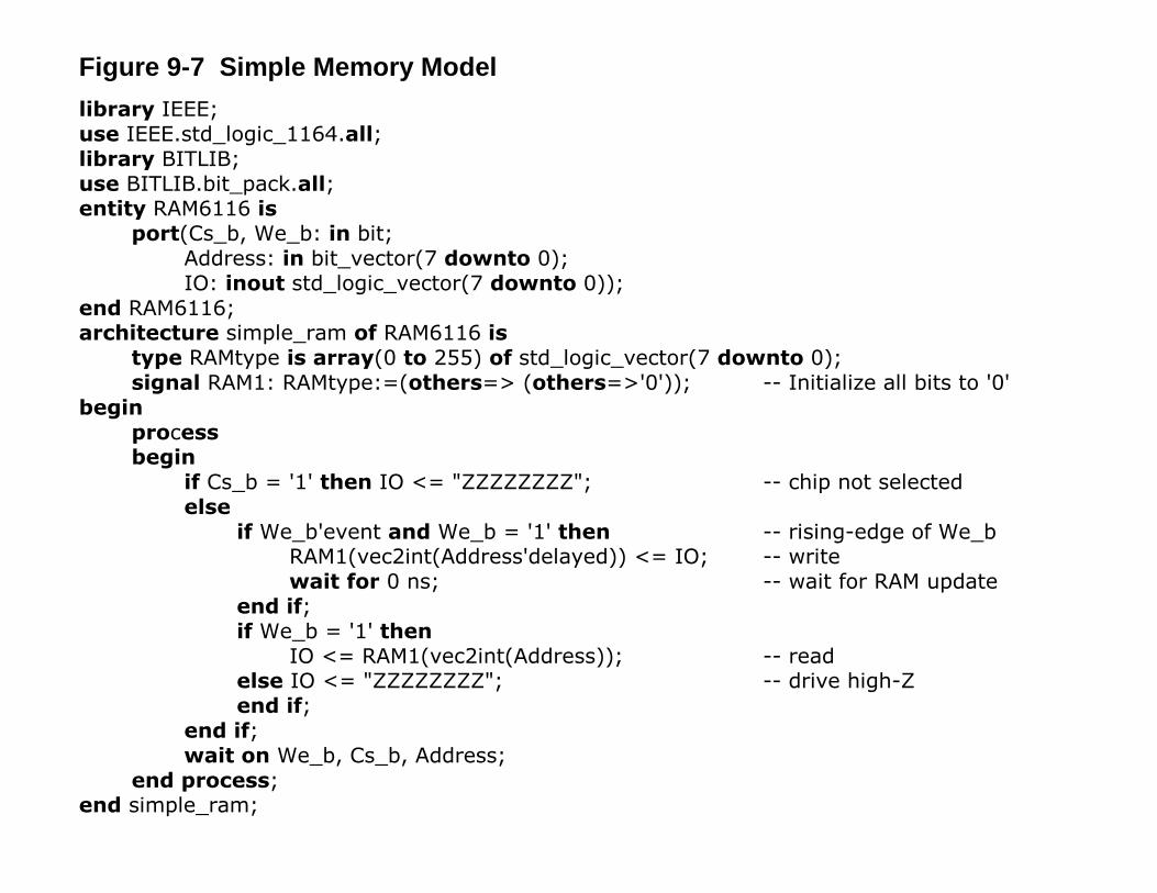
Figure 9-7 Simple Memory Modellibrary IEEE;use IEEE.std_logic_1164.all;library BITLIB;use BITLIB.bit_pack.all;entity RAM6116 is
port(Cs_b, We_b: in bit;Address: in bit_vector(7 downto 0);IO: inout std_logic_vector(7 downto 0));
end RAM6116;architecture simple_ram of RAM6116 is
type RAMtype is array(0 to 255) of std_logic_vector(7 downto 0);signal RAM1: RAMtype:=(others=> (others=>'0')); -- Initialize all bits to '0'
beginprocessbegin
if Cs_b = '1' then IO <= "ZZZZZZZZ"; -- chip not selectedelse
if We_b'event and We_b = '1' then -- rising-edge of We_bRAM1(vec2int(Address'delayed)) <= IO; -- writewait for 0 ns; -- wait for RAM update
end if;if We_b = '1' then
IO <= RAM1(vec2int(Address)); -- readelse IO <= "ZZZZZZZZ"; -- drive high-Zend if;
end if;wait on We_b, Cs_b, Address;
end process;end simple_ram;
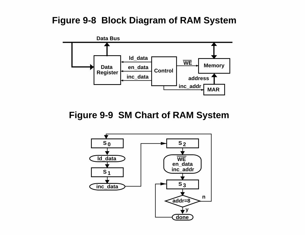
S 0
ld_data
inc_data
S 1
S 2
S 3
en_datainc_addr
addr=8
doney
n
WE
Data Bus
DataRegister
ld_data
en_data
inc_dataControl
inc_addr
Memory
address
MAR
WE
Figure 9-8 Block Diagram of RAM System
Figure 9-9 SM Chart of RAM System
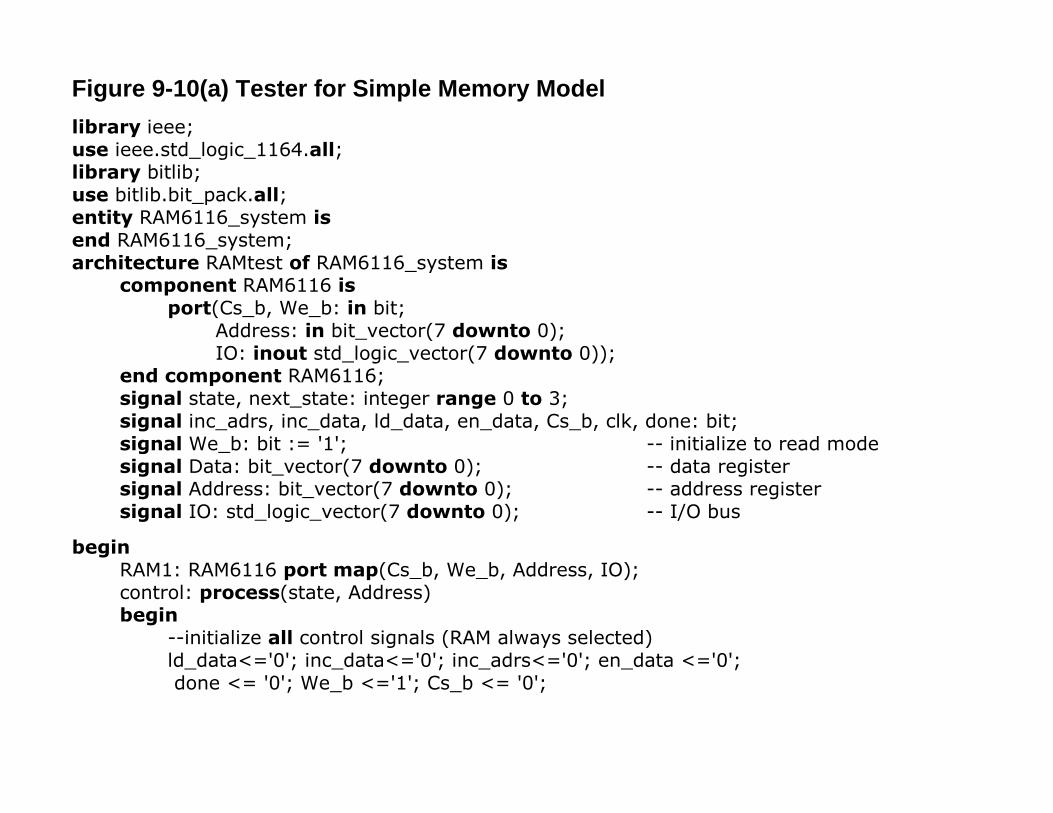
Figure 9-10(a) Tester for Simple Memory Modellibrary ieee;use ieee.std_logic_1164.all;library bitlib;use bitlib.bit_pack.all;entity RAM6116_system isend RAM6116_system;architecture RAMtest of RAM6116_system is
component RAM6116 isport(Cs_b, We_b: in bit;
Address: in bit_vector(7 downto 0);IO: inout std_logic_vector(7 downto 0));
end component RAM6116;signal state, next_state: integer range 0 to 3;signal inc_adrs, inc_data, ld_data, en_data, Cs_b, clk, done: bit;signal We_b: bit := '1'; -- initialize to read modesignal Data: bit_vector(7 downto 0); -- data registersignal Address: bit_vector(7 downto 0); -- address registersignal IO: std_logic_vector(7 downto 0); -- I/O bus
beginRAM1: RAM6116 port map(Cs_b, We_b, Address, IO);control: process(state, Address)begin
--initialize all control signals (RAM always selected)ld_data<='0'; inc_data<='0'; inc_adrs<='0'; en_data <='0'; done <= '0'; We_b <='1'; Cs_b <= '0';
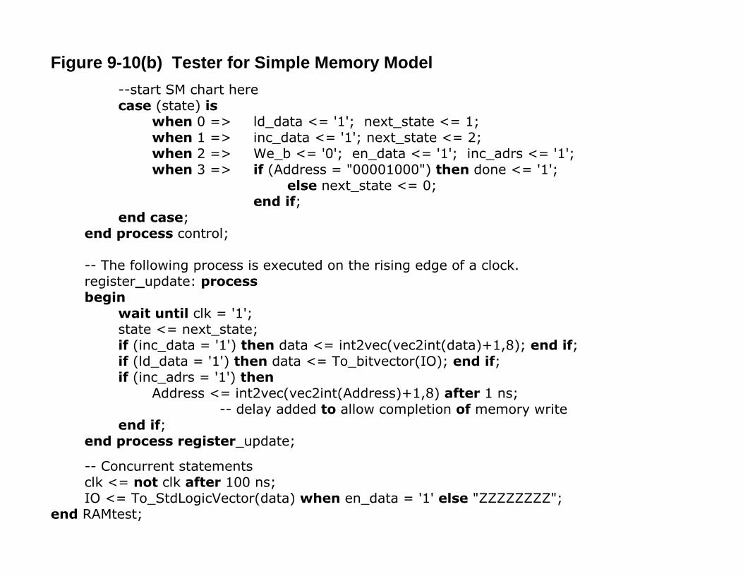
Figure 9-10(b) Tester for Simple Memory Model--start SM chart herecase (state) is
when 0 => ld_data <= '1'; next_state <= 1;when 1 => inc_data <= '1'; next_state <= 2;when 2 => We_b <= '0'; en_data <= '1'; inc_adrs <= '1';when 3 => if (Address = "00001000") then done <= '1';
else next_state <= 0;end if;
end case;end process control;
-- The following process is executed on the rising edge of a clock.register_update: processbegin
wait until clk = '1';state <= next_state;if (inc_data = '1') then data <= int2vec(vec2int(data)+1,8); end if;if (ld_data = '1') then data <= To_bitvector(IO); end if;if (inc_adrs = '1') then
Address <= int2vec(vec2int(Address)+1,8) after 1 ns;-- delay added to allow completion of memory write
end if;end process register_update;
-- Concurrent statementsclk <= not clk after 100 ns;IO <= To_StdLogicVector(data) when en_data = '1' else "ZZZZZZZZ";
end RAMtest;
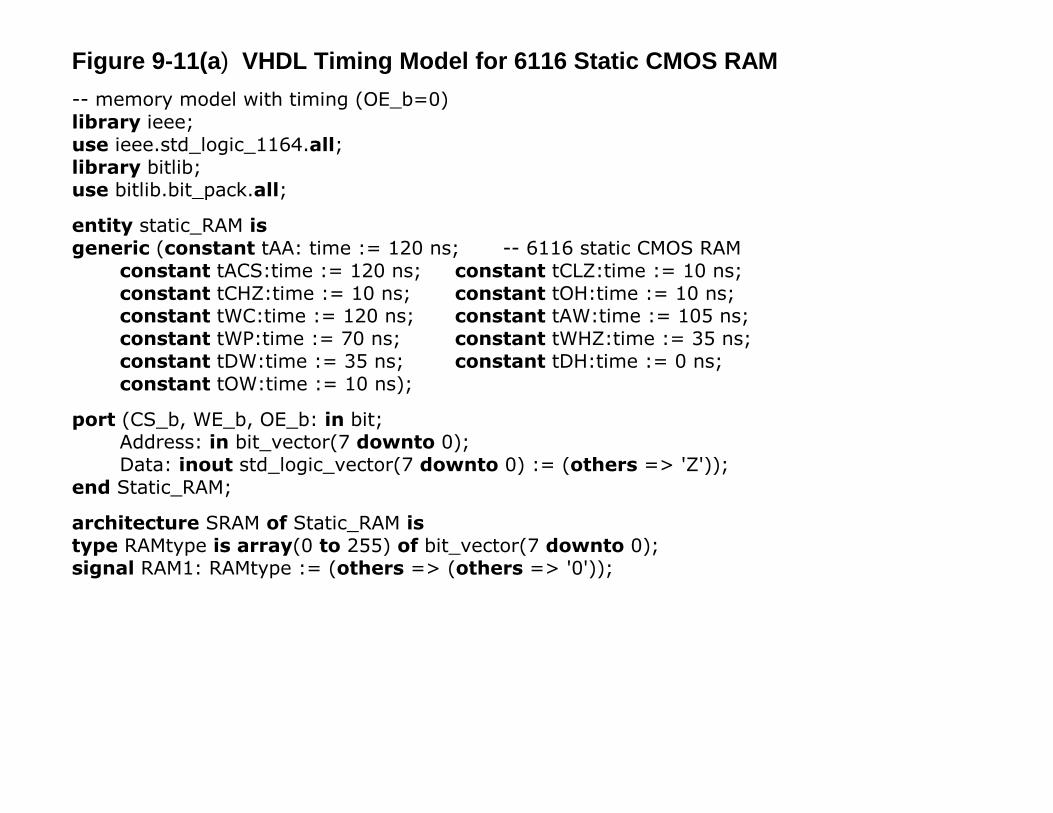
Figure 9-11(a) VHDL Timing Model for 6116 Static CMOS RAM-- memory model with timing (OE_b=0)library ieee;use ieee.std_logic_1164.all;library bitlib;use bitlib.bit_pack.all;
entity static_RAM isgeneric (constant tAA: time := 120 ns; -- 6116 static CMOS RAM
constant tACS:time := 120 ns; constant tCLZ:time := 10 ns;constant tCHZ:time := 10 ns; constant tOH:time := 10 ns;constant tWC:time := 120 ns; constant tAW:time := 105 ns;constant tWP:time := 70 ns; constant tWHZ:time := 35 ns;constant tDW:time := 35 ns; constant tDH:time := 0 ns;constant tOW:time := 10 ns);
port (CS_b, WE_b, OE_b: in bit;Address: in bit_vector(7 downto 0);Data: inout std_logic_vector(7 downto 0) := (others => 'Z'));
end Static_RAM;
architecture SRAM of Static_RAM istype RAMtype is array(0 to 255) of bit_vector(7 downto 0);signal RAM1: RAMtype := (others => (others => '0'));
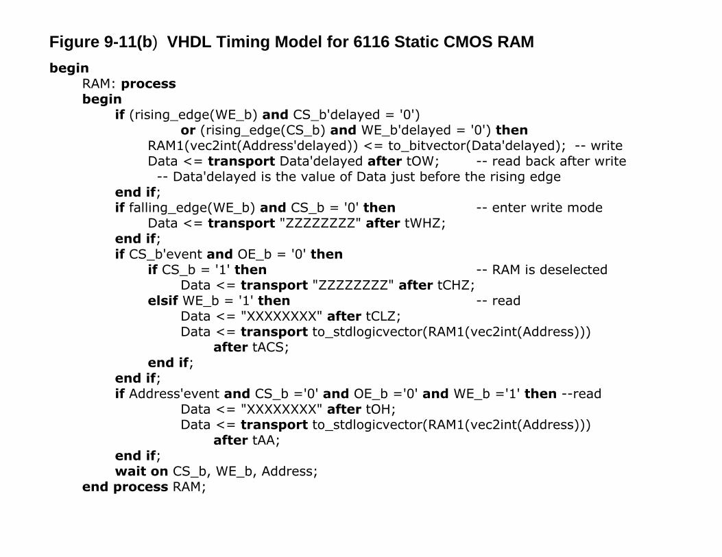
Figure 9-11(b) VHDL Timing Model for 6116 Static CMOS RAMbegin
RAM: processbegin
if (rising_edge(WE_b) and CS_b'delayed = '0')or (rising_edge(CS_b) and WE_b'delayed = '0') then
RAM1(vec2int(Address'delayed)) <= to_bitvector(Data'delayed); -- writeData <= transport Data'delayed after tOW; -- read back after write -- Data'delayed is the value of Data just before the rising edge
end if;if falling_edge(WE_b) and CS_b = '0' then -- enter write mode
Data <= transport "ZZZZZZZZ" after tWHZ;end if;if CS_b'event and OE_b = '0' then
if CS_b = '1' then -- RAM is deselectedData <= transport "ZZZZZZZZ" after tCHZ;
elsif WE_b = '1' then -- readData <= "XXXXXXXX" after tCLZ;Data <= transport to_stdlogicvector(RAM1(vec2int(Address)))
after tACS;end if;
end if;if Address'event and CS_b ='0' and OE_b ='0' and WE_b ='1' then --read
Data <= "XXXXXXXX" after tOH;Data <= transport to_stdlogicvector(RAM1(vec2int(Address)))
after tAA;end if;wait on CS_b, WE_b, Address;
end process RAM;
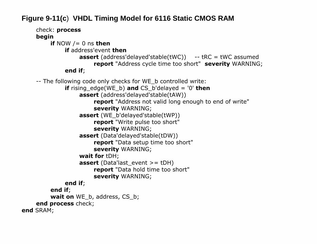
Figure 9-11(c) VHDL Timing Model for 6116 Static CMOS RAMcheck: processbegin
if NOW /= 0 ns thenif address'event then
assert (address'delayed'stable(tWC)) -- tRC = tWC assumedreport "Address cycle time too short" severity WARNING;
end if;
-- The following code only checks for WE_b controlled write:if rising_edge(WE_b) and CS_b'delayed = '0' then
assert (address'delayed'stable(tAW))report "Address not valid long enough to end of write"severity WARNING;
assert (WE_b'delayed'stable(tWP))report "Write pulse too short"severity WARNING;
assert (Data'delayed'stable(tDW))report "Data setup time too short"severity WARNING;
wait for tDH;assert (Data'last_event >= tDH)
report "Data hold time too short"severity WARNING;
end if;end if;wait on WE_b, address, CS_b;
end process check;end SRAM;
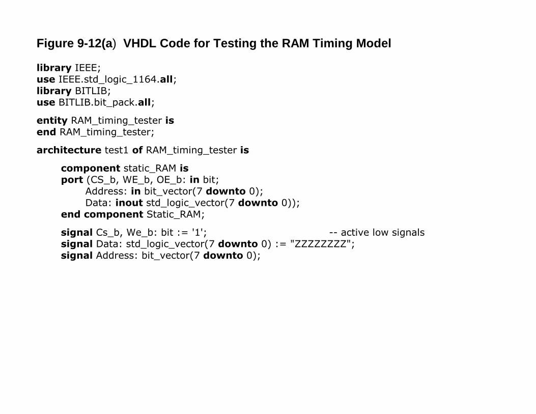
Figure 9-12(a) VHDL Code for Testing the RAM Timing Model
library IEEE;use IEEE.std_logic_1164.all;library BITLIB;use BITLIB.bit_pack.all;
entity RAM_timing_tester isend RAM_timing_tester;
architecture test1 of RAM_timing_tester is
component static_RAM isport (CS_b, WE_b, OE_b: in bit;
Address: in bit_vector(7 downto 0);Data: inout std_logic_vector(7 downto 0));
end component Static_RAM;
signal Cs_b, We_b: bit := '1'; -- active low signalssignal Data: std_logic_vector(7 downto 0) := "ZZZZZZZZ";signal Address: bit_vector(7 downto 0);
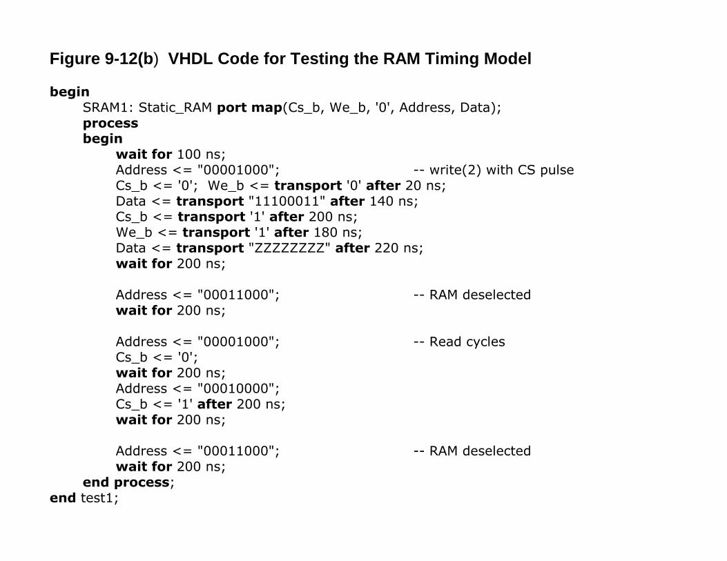
Figure 9-12(b) VHDL Code for Testing the RAM Timing Model
beginSRAM1: Static_RAM port map(Cs_b, We_b, '0', Address, Data);processbegin
wait for 100 ns;Address <= "00001000"; -- write(2) with CS pulseCs_b <= '0'; We_b <= transport '0' after 20 ns;Data <= transport "11100011" after 140 ns;Cs_b <= transport '1' after 200 ns;We_b <= transport '1' after 180 ns;Data <= transport "ZZZZZZZZ" after 220 ns;wait for 200 ns;
Address <= "00011000"; -- RAM deselectedwait for 200 ns;
Address <= "00001000"; -- Read cyclesCs_b <= '0';wait for 200 ns;Address <= "00010000";Cs_b <= '1' after 200 ns;wait for 200 ns;
Address <= "00011000"; -- RAM deselectedwait for 200 ns;
end process;end test1;
/address
/cs_b
/we_b
/data XXXXXXXX
00001000
11100011 XXXXXXXX
00010000
00000000
00011000
/address
/cs_b
/we_b
/data
00000000
XXXXXXXXZZZZZZZZ
00001000
ZZZZZZZZ 11100011
00011000
ZZZZZZZZ
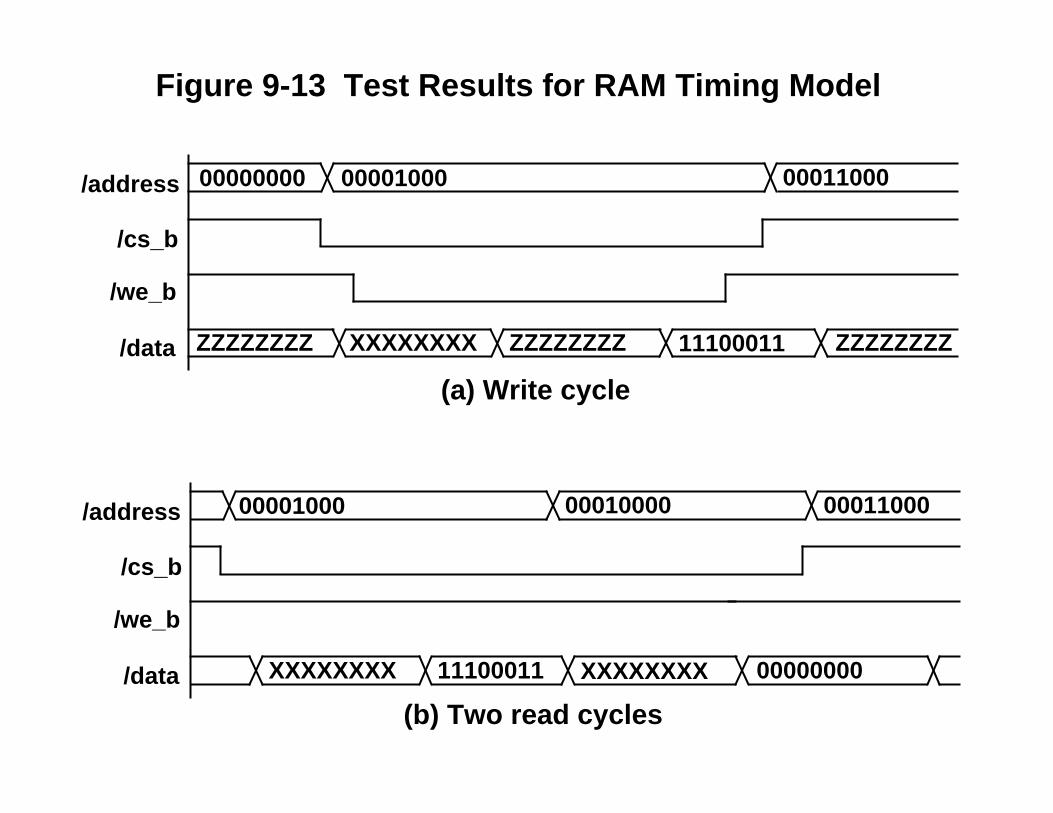
Figure 9-13 Test Results for RAM Timing Model
(a) Write cycle
(b) Two read cycles
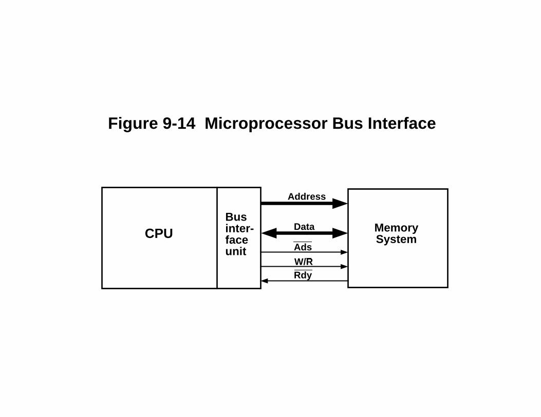
Businter-faceunit
CPU MemorySystem
Address
Data
Ads
W/RRdy
Figure 9-14 Microprocessor Bus Interface
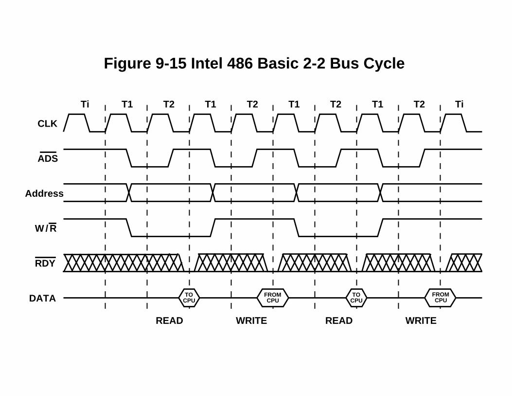
TOCPU
FROMCPU
TOCPU
FROMCPU
READ WRITE READ WRITE
CLK
ADS
Address
W / R
RDY
DATA
TiTi T1 T2 T1 T2 T1 T2 T1 T2
Figure 9-15 Intel 486 Basic 2-2 Bus Cycle
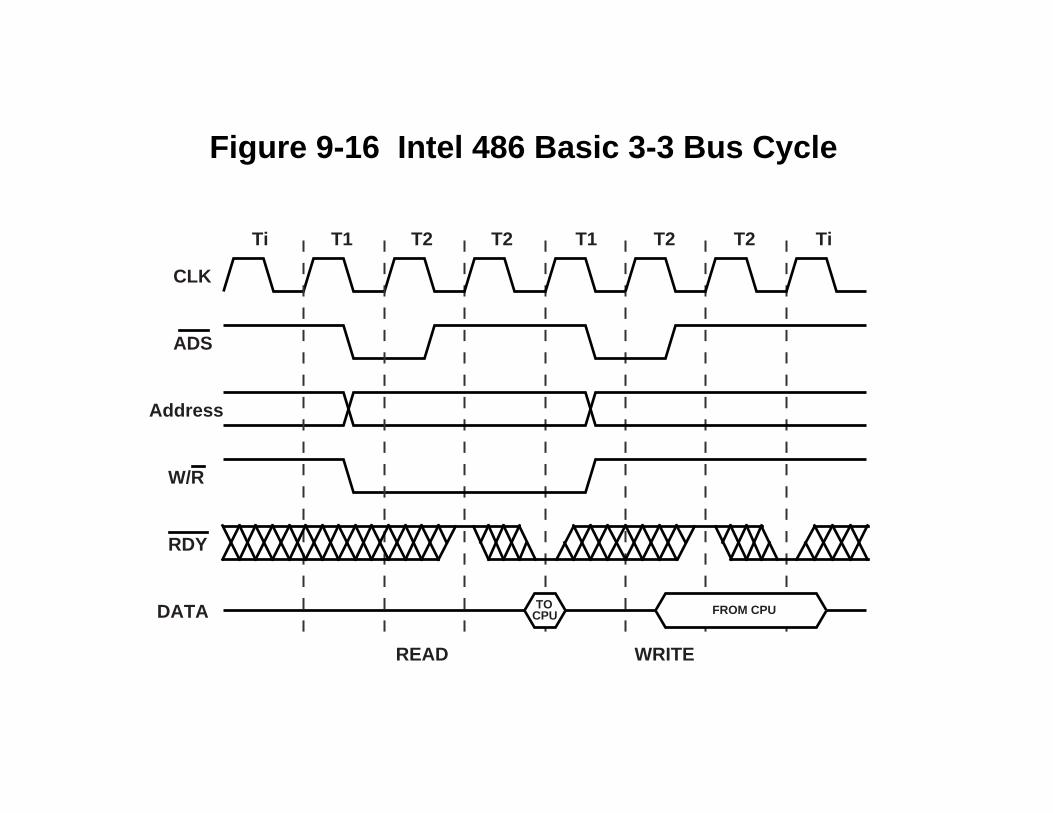
TOCPU FROM CPU
READ WRITE
Ti T1 T2 T2 T1 T2 T2 Ti
CLK
ADS
Address
W/R
RDY
DATA
Figure 9-16 Intel 486 Basic 3-3 Bus Cycle
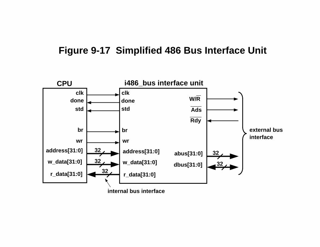
doneclk
br
wr
w_data[31:0]
address[31:0]
W/R
Ads
Rdy
doneclk
br
wr
w_data[31:0]
address[31:0] abus[31:0]
dbus[31:0]
i486_bus interface unit
32
std
r_data[31:0] r_data[31:0]
std
CPU
32
32
32
32
external businterface
internal bus interface
Figure 9-17 Simplified 486 Bus Interface Unit
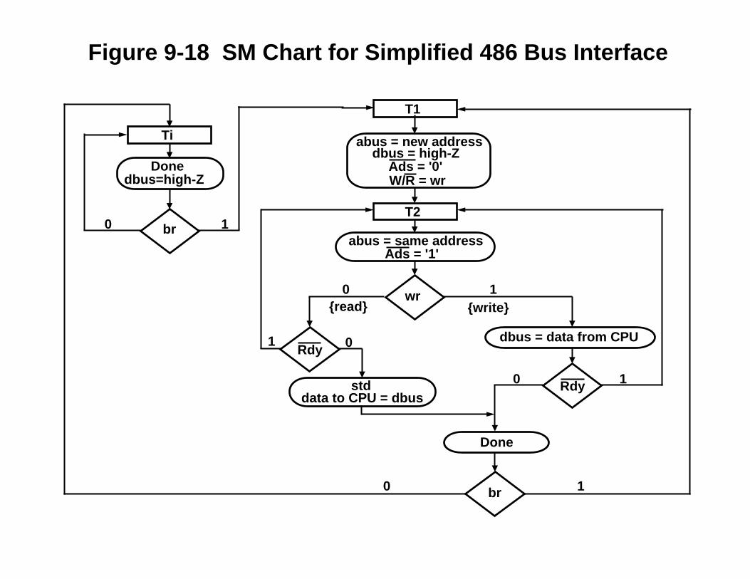
Ti
Donedbus=high-Z
br 10
T1
abus = new address
Ads = '0'W/R = wr
T2
wr
Rdy
0
1 0
stddata to CPU = dbus
dbus = data from CPU
br0
0 1
1
1
dbus = high-Z
abus = same addressAds = '1'
Done
{read} {write}
Rdy
Figure 9-18 SM Chart for Simplified 486 Bus Interface
CLK
RDY
DATA
Tx Tx Tx
t17t16
t23t22
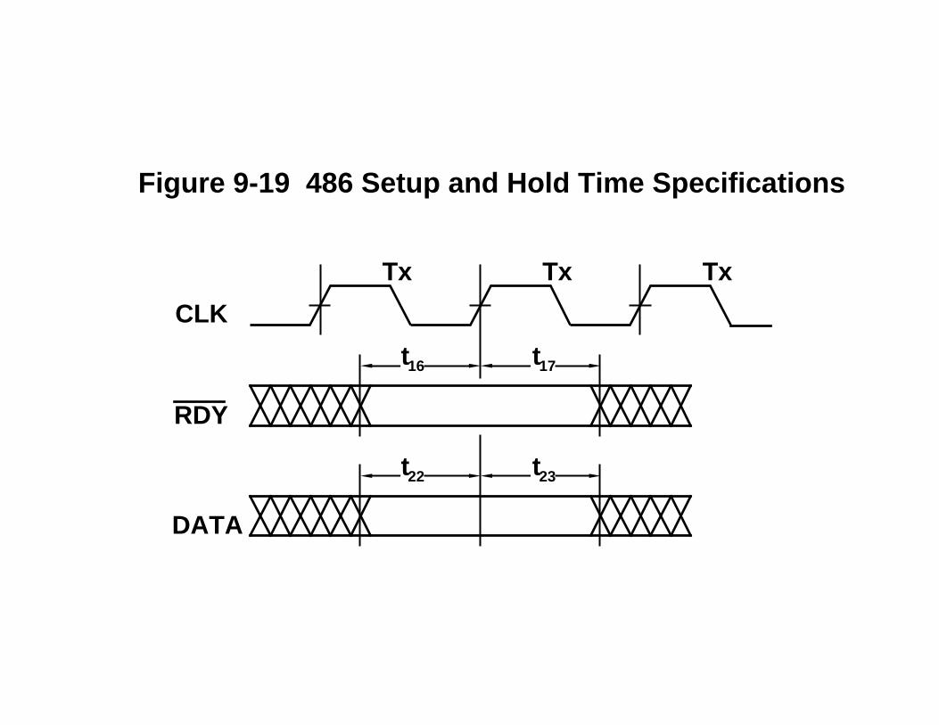
Figure 9-19 486 Setup and Hold Time Specifications
CLK
Address, Ads, W/R
Data (Write)(successive cycles)
Tx Tx Tx
t 6 maxt 6 min
VALID n VALID n+1
t 10 maxt10 min
VALID n VALID n+1
Data (Write)to High-Z
t11t10 min
VALID
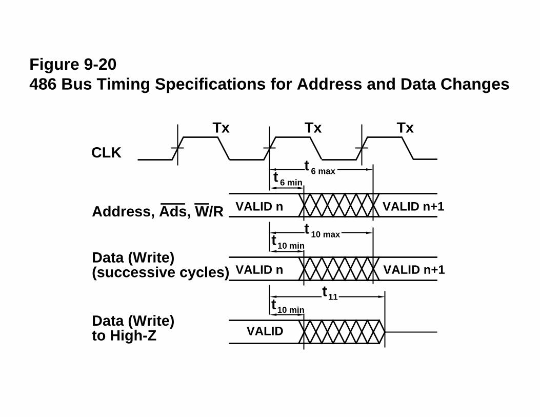
Figure 9-20486 Bus Timing Specifications for Address and Data Changes
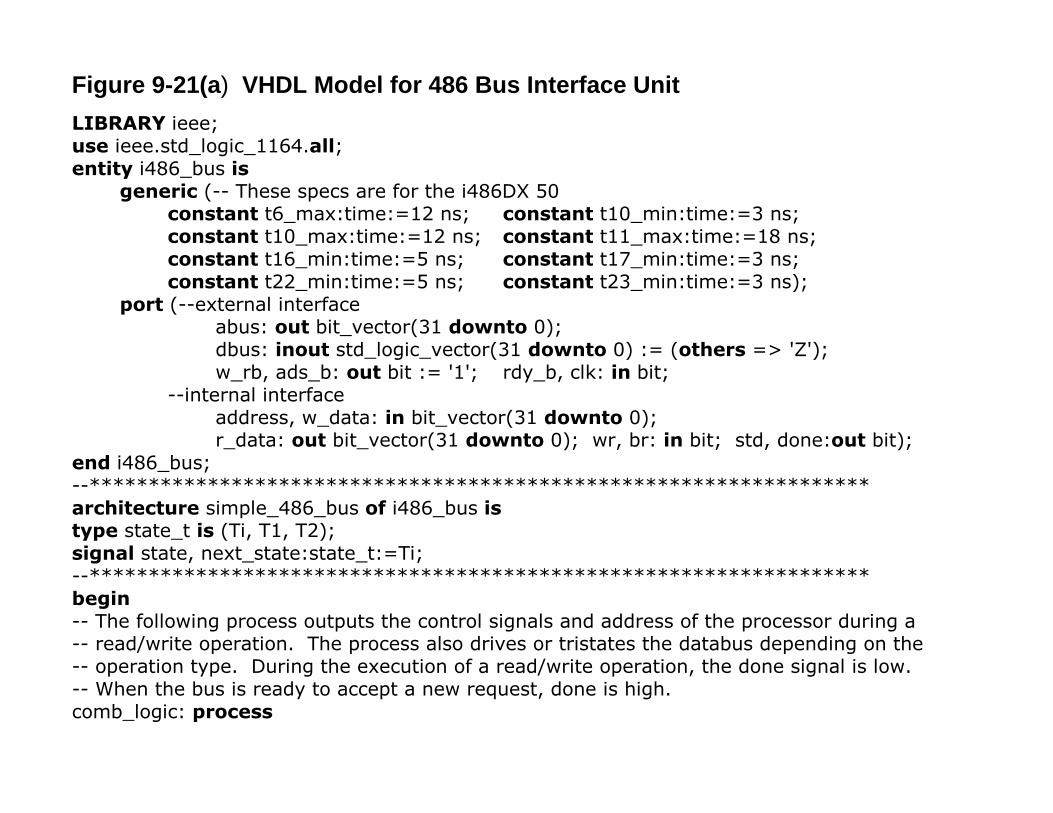
Figure 9-21(a) VHDL Model for 486 Bus Interface UnitLIBRARY ieee;use ieee.std_logic_1164.all;entity i486_bus is
generic (-- These specs are for the i486DX 50constant t6_max:time:=12 ns; constant t10_min:time:=3 ns;constant t10_max:time:=12 ns; constant t11_max:time:=18 ns;constant t16_min:time:=5 ns; constant t17_min:time:=3 ns;constant t22_min:time:=5 ns; constant t23_min:time:=3 ns);
port (--external interfaceabus: out bit_vector(31 downto 0);dbus: inout std_logic_vector(31 downto 0) := (others => 'Z');w_rb, ads_b: out bit := '1'; rdy_b, clk: in bit;
--internal interfaceaddress, w_data: in bit_vector(31 downto 0);r_data: out bit_vector(31 downto 0); wr, br: in bit; std, done:out bit);
end i486_bus;--******************************************************************architecture simple_486_bus of i486_bus istype state_t is (Ti, T1, T2);signal state, next_state:state_t:=Ti;--******************************************************************begin-- The following process outputs the control signals and address of the processor during a-- read/write operation. The process also drives or tristates the databus depending on the-- operation type. During the execution of a read/write operation, the done signal is low.-- When the bus is ready to accept a new request, done is high.comb_logic: process
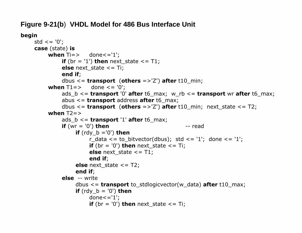
Figure 9-21(b) VHDL Model for 486 Bus Interface Unitbegin
std <= '0';case (state) is
when Ti=> done<='1';if (br = '1') then next_state <= T1;else next_state <= Ti;end if;dbus <= transport (others =>'Z') after t10_min;
when T1=> done <= '0';ads_b <= transport '0' after t6_max; w_rb <= transport wr after t6_max;abus <= transport address after t6_max;dbus <= transport (others =>'Z') after t10_min; next_state <= T2;
when T2=>ads_b <= transport '1' after t6_max;if (wr = '0') then -- read
if (rdy_b ='0') thenr_data <= to_bitvector(dbus); std <= '1'; done <= '1';if (br = '0') then next_state <= Ti;else next_state <= T1;end if;
else next_state <= T2;end if;
else -- writedbus <= transport to_stdlogicvector(w_data) after t10_max;if (rdy_b = '0') then
done<='1';if (br = '0') then next_state <= Ti;
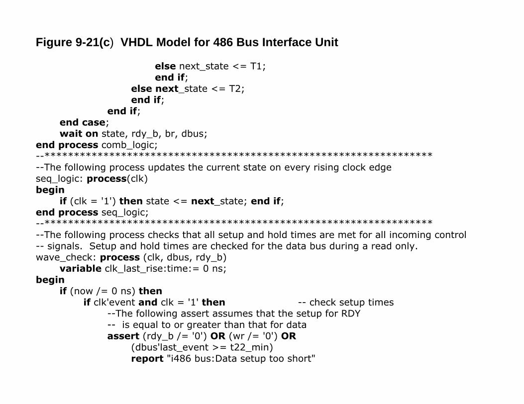
Figure 9-21(c) VHDL Model for 486 Bus Interface Unit
else next_state <= T1;end if;
else next_state <= T2;end if;
end if;end case;wait on state, rdy_b, br, dbus;
end process comb_logic;--******************************************************************--The following process updates the current state on every rising clock edgeseq_logic: process(clk)begin
if (clk = '1') then state <= next_state; end if;end process seq_logic;--******************************************************************--The following process checks that all setup and hold times are met for all incoming control-- signals. Setup and hold times are checked for the data bus during a read only.wave_check: process (clk, dbus, rdy_b)
variable clk_last_rise:time:= 0 ns;begin
if (now /= 0 ns) thenif clk'event and clk = '1' then -- check setup times
--The following assert assumes that the setup for RDY-- is equal to or greater than that for dataassert (rdy_b /= '0') OR (wr /= '0') OR
(dbus'last_event >= t22_min)report "i486 bus:Data setup too short"
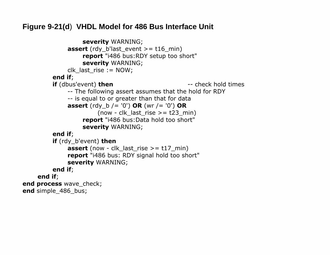
Figure 9-21(d) VHDL Model for 486 Bus Interface Unit
severity WARNING;assert (rdy_b'last_event >= t16_min)
report "i486 bus:RDY setup too short"severity WARNING;
clk_last_rise := NOW;end if;if (dbus'event) then -- check hold times
-- The following assert assumes that the hold for RDY-- is equal to or greater than that for dataassert (rdy_b /= '0') OR (wr /= '0') OR
(now - clk_last_rise >= t23_min)report "i486 bus:Data hold too short"severity WARNING;
end if;if (rdy_b'event) then
assert (now - clk_last_rise >= t17_min)report "i486 bus: RDY signal hold too short"severity WARNING;
end if;end if;
end process wave_check;end simple_486_bus;
addr[14:0]data[15:8]
CS WE OE
addr[14:0]data[7:0]
CS WE OE
addr[14:0]data[23:16]
CS WE OE
W/R
abus[31:0]
addr[14:0]data[31:24]
CS WE OE
CPU (or Tester) memory controller
address decoder
Ram3 Ram2 Ram1 Ram0
WE
Ads
Rdy
32
32
32
15
8 88 815 15 15 15
15
doneclk
br
wr
w_data[31:0]
address[31:0]
W/R
Ads
Rdy
doneclk
br
wr
w_data[31:0]
address[31:0] abus[31:0]
dbus[31:0]
i486_bus interface unit
32
std
r_data[31:0] r_data[31:0]
std
clk
CS
CS132
32
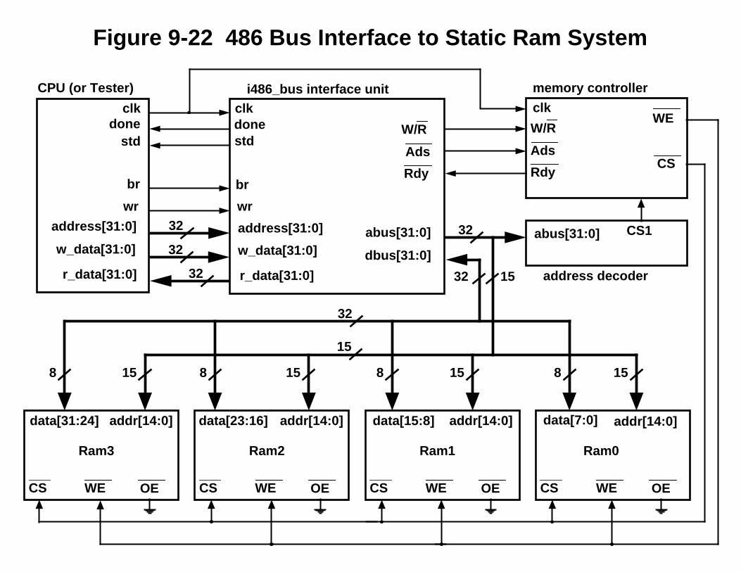
Figure 9-22 486 Bus Interface to Static Ram System
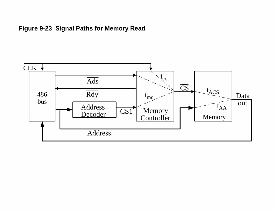
Figure 9-23 Signal Paths for Memory Read
486bus
AddressDecoder Memory
Controller Memory
Ads
CS1
CS
Address
Dataout
tACS
tAA
tmcRdy
CLKtcc
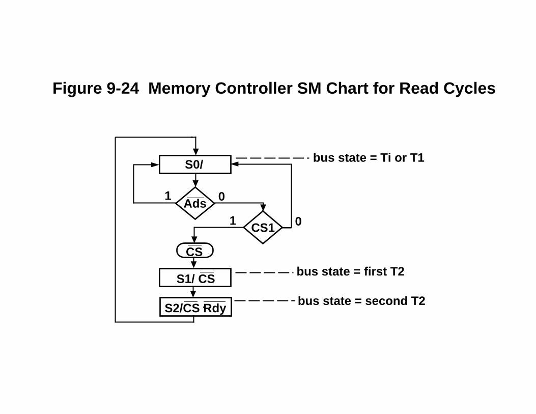
Ads
CS1
CS
S0/
S1/ CS
S2/CS Rdy
bus state = Ti or T1
bus state = first T2
bus state = second T2
0
1 0
1
Figure 9-24 Memory Controller SM Chart for Read Cycles
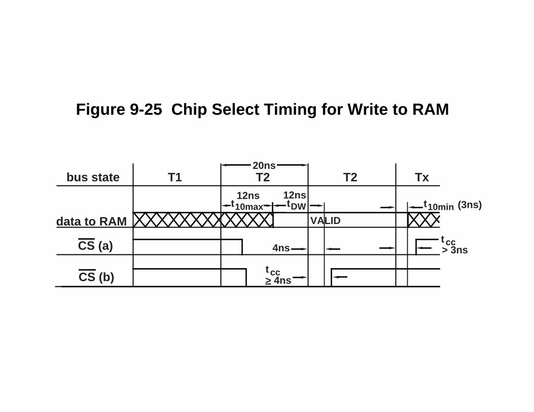
T1 T2 T2 Txbus state
data to RAM
CS (a)
t10max tDW t10min (3ns)
tcc
VALID
> 4nstcc
> 3ns
20ns
12ns 12ns
4ns
CS (b)
Figure 9-25 Chip Select Timing for Write to RAM
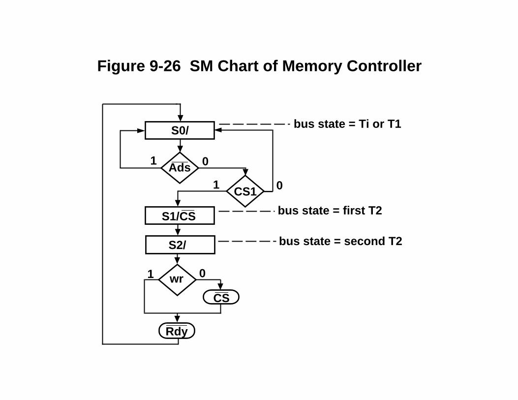
Ads
CS1
S0/
S1/CS
S2/
bus state = Ti or T1
bus state = first T2
bus state = second T2
0
1 0
1
wr
CS
Rdy
1 0
Figure 9-26 SM Chart of Memory Controller
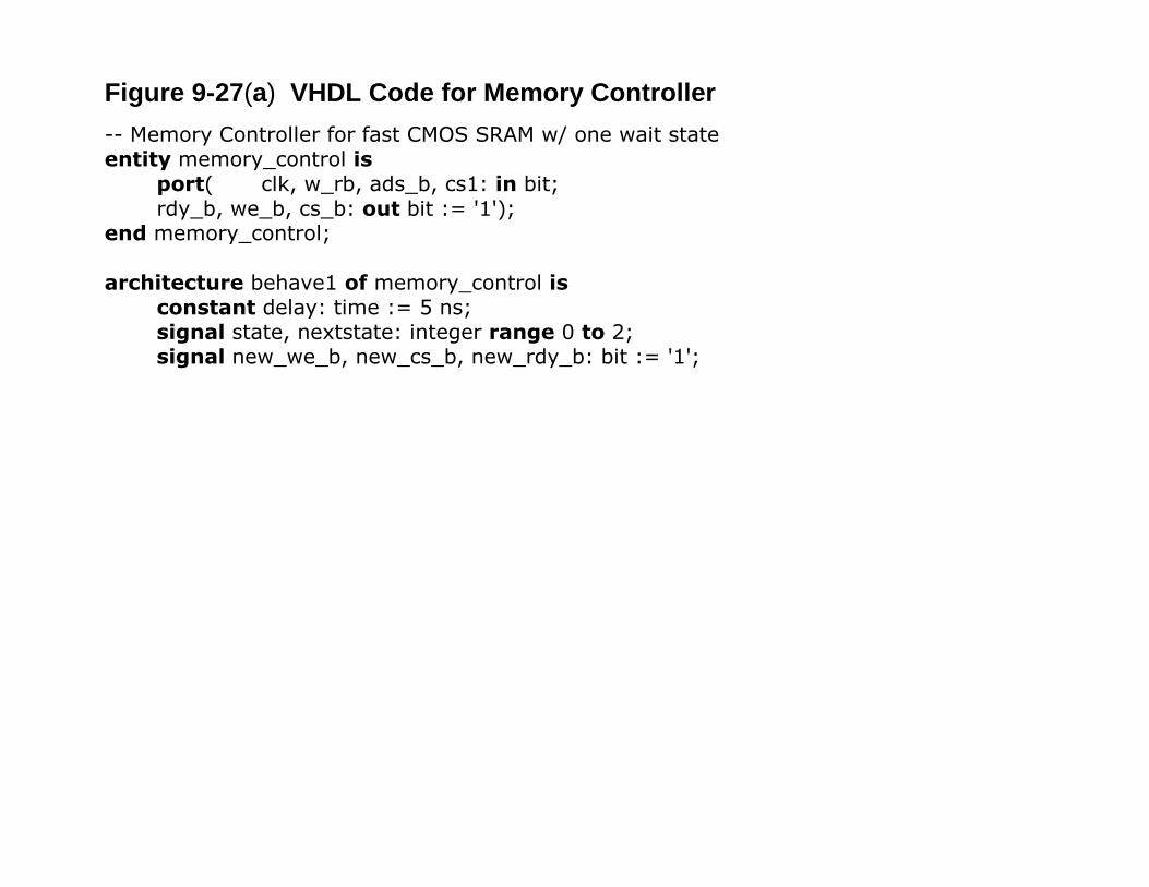
Figure 9-27(a) VHDL Code for Memory Controller-- Memory Controller for fast CMOS SRAM w/ one wait stateentity memory_control is
port( clk, w_rb, ads_b, cs1: in bit;rdy_b, we_b, cs_b: out bit := '1');
end memory_control;
architecture behave1 of memory_control isconstant delay: time := 5 ns;signal state, nextstate: integer range 0 to 2;signal new_we_b, new_cs_b, new_rdy_b: bit := '1';
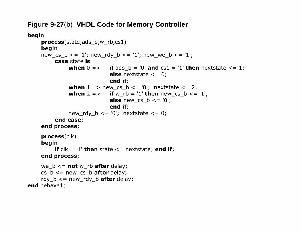
Figure 9-27(b) VHDL Code for Memory Controllerbegin
process(state,ads_b,w_rb,cs1)beginnew_cs_b <= '1'; new_rdy_b <= '1'; new_we_b <= '1';
case state iswhen 0 => if ads_b = '0' and cs1 = '1' then nextstate <= 1;
else nextstate <= 0;end if;
when 1 => new_cs_b <= '0'; nextstate <= 2;when 2 => if w_rb = '1' then new_cs_b <= '1';
else new_cs_b <= '0';end if;
new_rdy_b <= '0'; nextstate <= 0;end case;
end process;
process(clk)begin
if clk = '1' then state <= nextstate; end if;end process;
we_b <= not w_rb after delay;cs_b <= new_cs_b after delay;rdy_b <= new_rdy_b after delay;
end behave1;
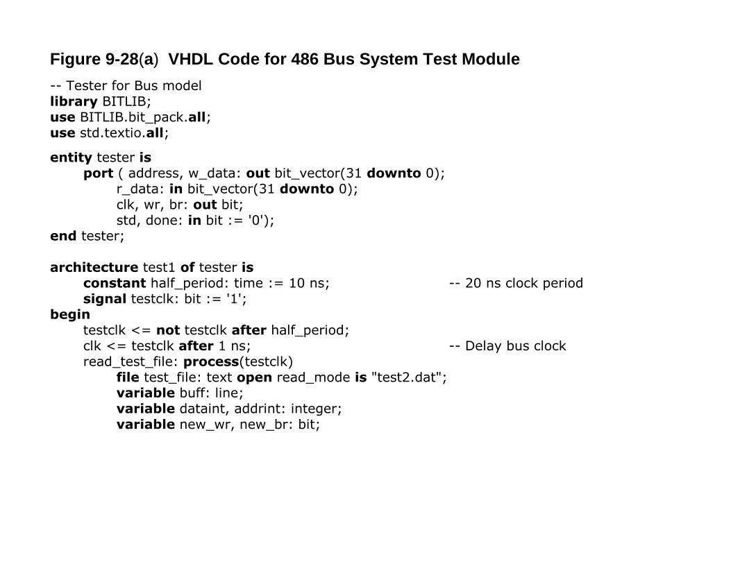
Figure 9-28(a) VHDL Code for 486 Bus System Test Module-- Tester for Bus modellibrary BITLIB;use BITLIB.bit_pack.all;use std.textio.all;
entity tester isport ( address, w_data: out bit_vector(31 downto 0);
r_data: in bit_vector(31 downto 0);clk, wr, br: out bit;std, done: in bit := '0');
end tester;
architecture test1 of tester isconstant half_period: time := 10 ns; -- 20 ns clock periodsignal testclk: bit := '1';
begintestclk <= not testclk after half_period;clk <= testclk after 1 ns; -- Delay bus clockread_test_file: process(testclk)
file test_file: text open read_mode is "test2.dat";variable buff: line;variable dataint, addrint: integer;variable new_wr, new_br: bit;
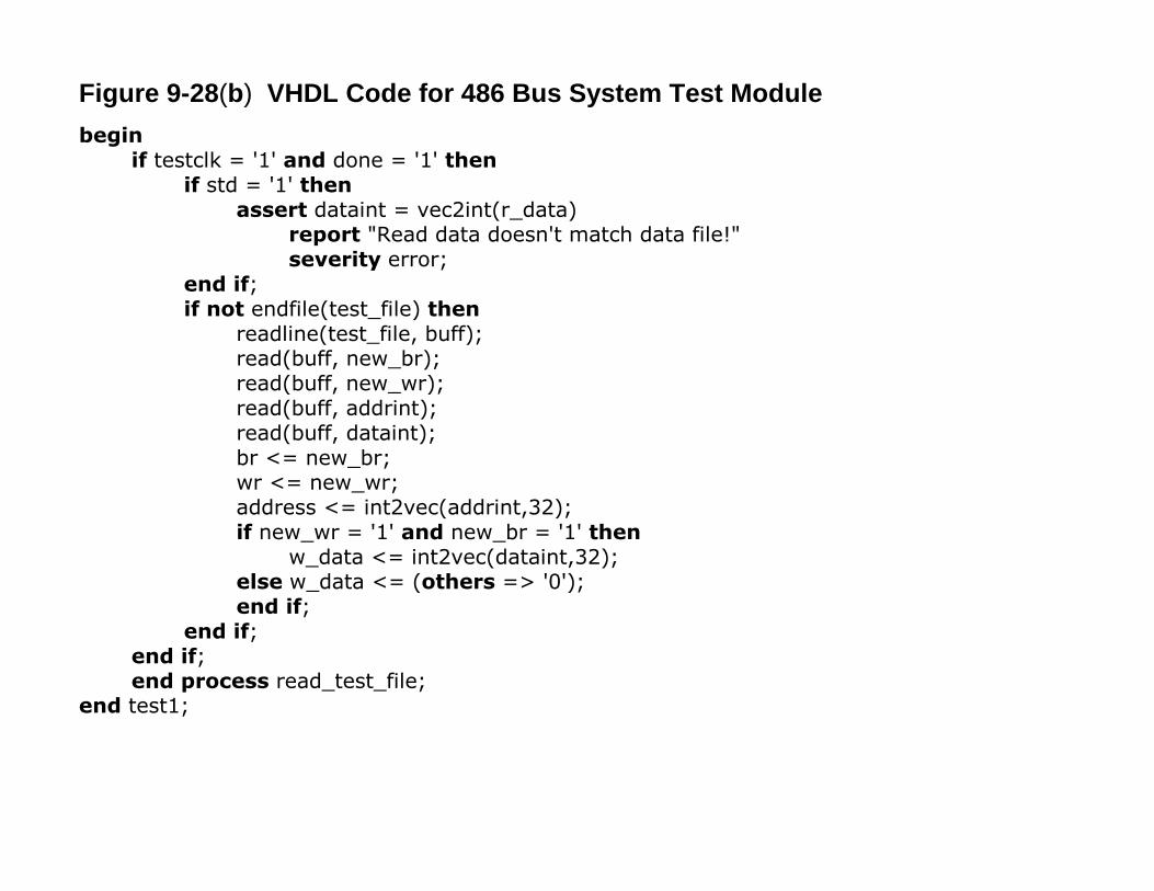
Figure 9-28(b) VHDL Code for 486 Bus System Test Modulebegin
if testclk = '1' and done = '1' thenif std = '1' then
assert dataint = vec2int(r_data)report "Read data doesn't match data file!"severity error;
end if;if not endfile(test_file) then
readline(test_file, buff);read(buff, new_br);read(buff, new_wr);read(buff, addrint);read(buff, dataint);br <= new_br;wr <= new_wr;address <= int2vec(addrint,32);if new_wr = '1' and new_br = '1' then
w_data <= int2vec(dataint,32);else w_data <= (others => '0');end if;
end if;end if;end process read_test_file;
end test1;
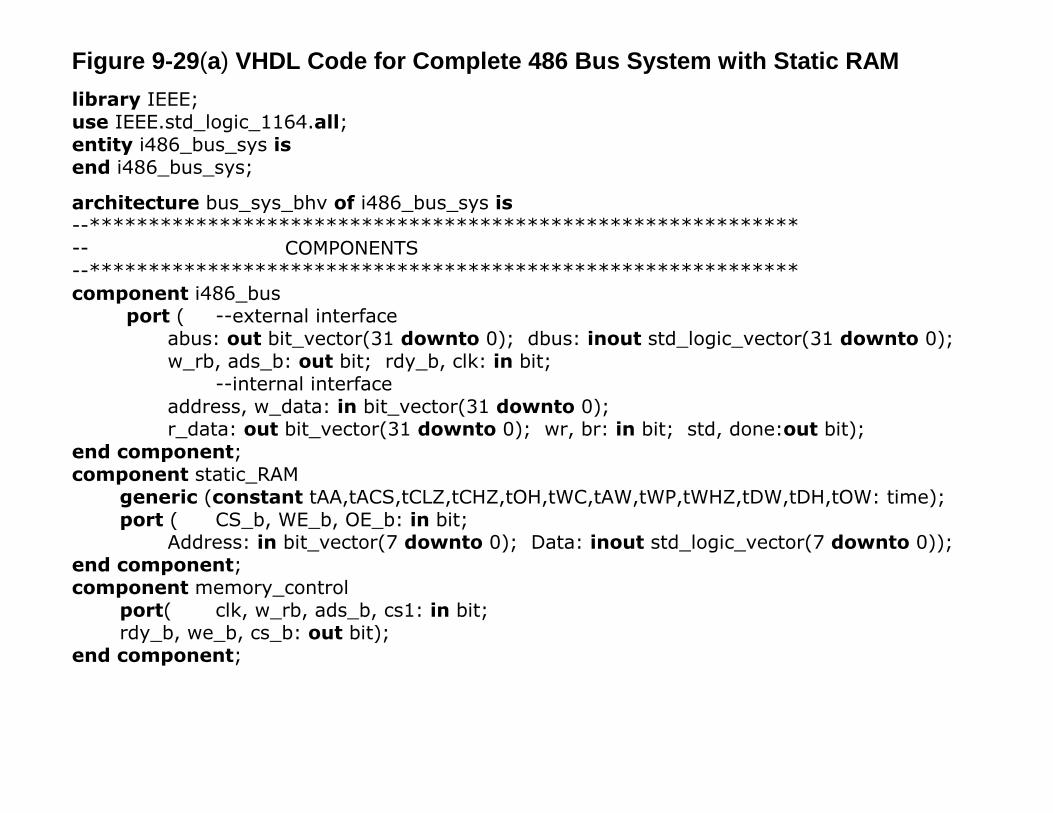
Figure 9-29(a) VHDL Code for Complete 486 Bus System with Static RAMlibrary IEEE;use IEEE.std_logic_1164.all;entity i486_bus_sys isend i486_bus_sys;
architecture bus_sys_bhv of i486_bus_sys is--************************************************************-- COMPONENTS--************************************************************component i486_bus
port ( --external interfaceabus: out bit_vector(31 downto 0); dbus: inout std_logic_vector(31 downto 0);w_rb, ads_b: out bit; rdy_b, clk: in bit;
--internal interfaceaddress, w_data: in bit_vector(31 downto 0);r_data: out bit_vector(31 downto 0); wr, br: in bit; std, done:out bit);
end component;component static_RAM
generic (constant tAA,tACS,tCLZ,tCHZ,tOH,tWC,tAW,tWP,tWHZ,tDW,tDH,tOW: time);port ( CS_b, WE_b, OE_b: in bit;
Address: in bit_vector(7 downto 0); Data: inout std_logic_vector(7 downto 0));end component;component memory_control
port( clk, w_rb, ads_b, cs1: in bit;rdy_b, we_b, cs_b: out bit);
end component;
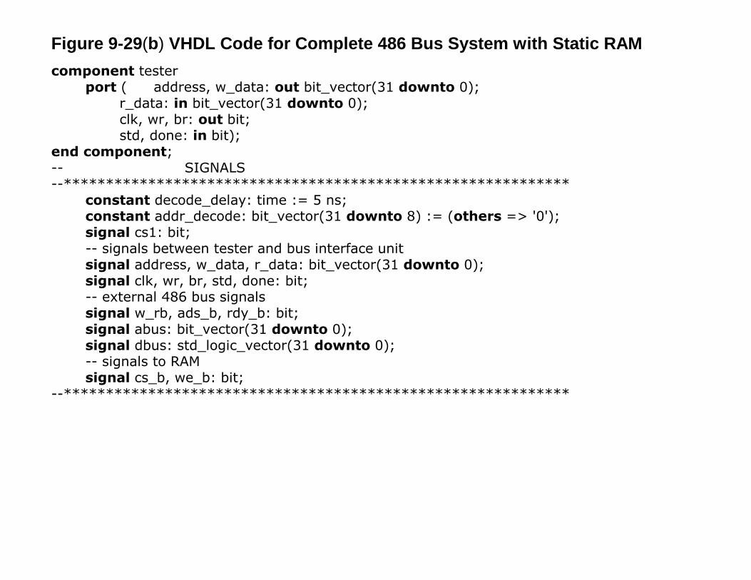
Figure 9-29(b) VHDL Code for Complete 486 Bus System with Static RAMcomponent tester
port ( address, w_data: out bit_vector(31 downto 0);r_data: in bit_vector(31 downto 0);clk, wr, br: out bit;std, done: in bit);
end component;-- SIGNALS--************************************************************
constant decode_delay: time := 5 ns;constant addr_decode: bit_vector(31 downto 8) := (others => '0');signal cs1: bit;-- signals between tester and bus interface unitsignal address, w_data, r_data: bit_vector(31 downto 0);signal clk, wr, br, std, done: bit;-- external 486 bus signalssignal w_rb, ads_b, rdy_b: bit;signal abus: bit_vector(31 downto 0);signal dbus: std_logic_vector(31 downto 0);-- signals to RAMsignal cs_b, we_b: bit;
--************************************************************
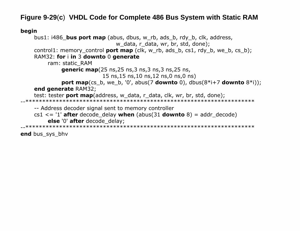
Figure 9-29(c) VHDL Code for Complete 486 Bus System with Static RAM
beginbus1: i486_bus port map (abus, dbus, w_rb, ads_b, rdy_b, clk, address,
w_data, r_data, wr, br, std, done);control1: memory_control port map (clk, w_rb, ads_b, cs1, rdy_b, we_b, cs_b);RAM32: for i in 3 downto 0 generate
ram: static_RAMgeneric map(25 ns,25 ns,3 ns,3 ns,3 ns,25 ns,
15 ns,15 ns,10 ns,12 ns,0 ns,0 ns)port map(cs_b, we_b, '0', abus(7 downto 0), dbus(8*i+7 downto 8*i));
end generate RAM32;test: tester port map(address, w_data, r_data, clk, wr, br, std, done);
--********************************************************************-- Address decoder signal sent to memory controllercs1 <= '1' after decode_delay when (abus(31 downto 8) = addr_decode)
else '0' after decode_delay;--********************************************************************end bus_sys_bhv
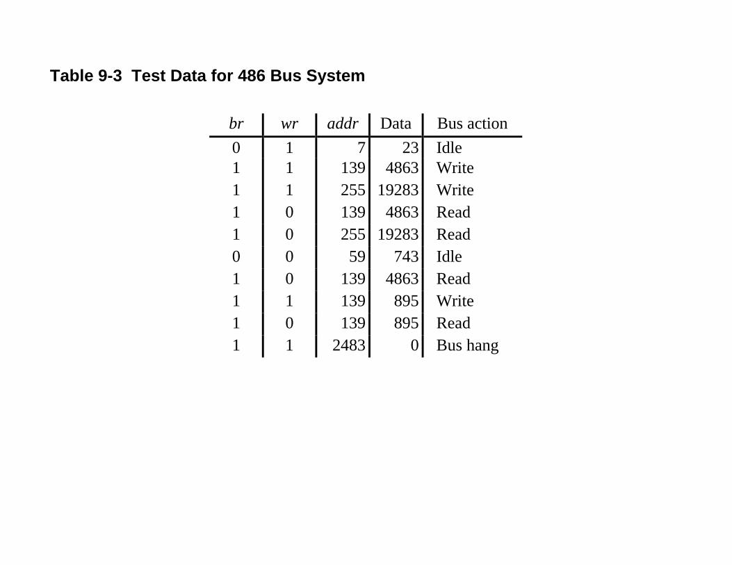
Table 9-3 Test Data for 486 Bus System
br wr addr Data Bus action0 1 7 23 Idle1 1 139 4863 Write1 1 255 19283 Write1 0 139 4863 Read1 0 255 19283 Read0 0 59 743 Idle1 0 139 4863 Read1 1 139 895 Write1 0 139 895 Read1 1 2483 0 Bus hang
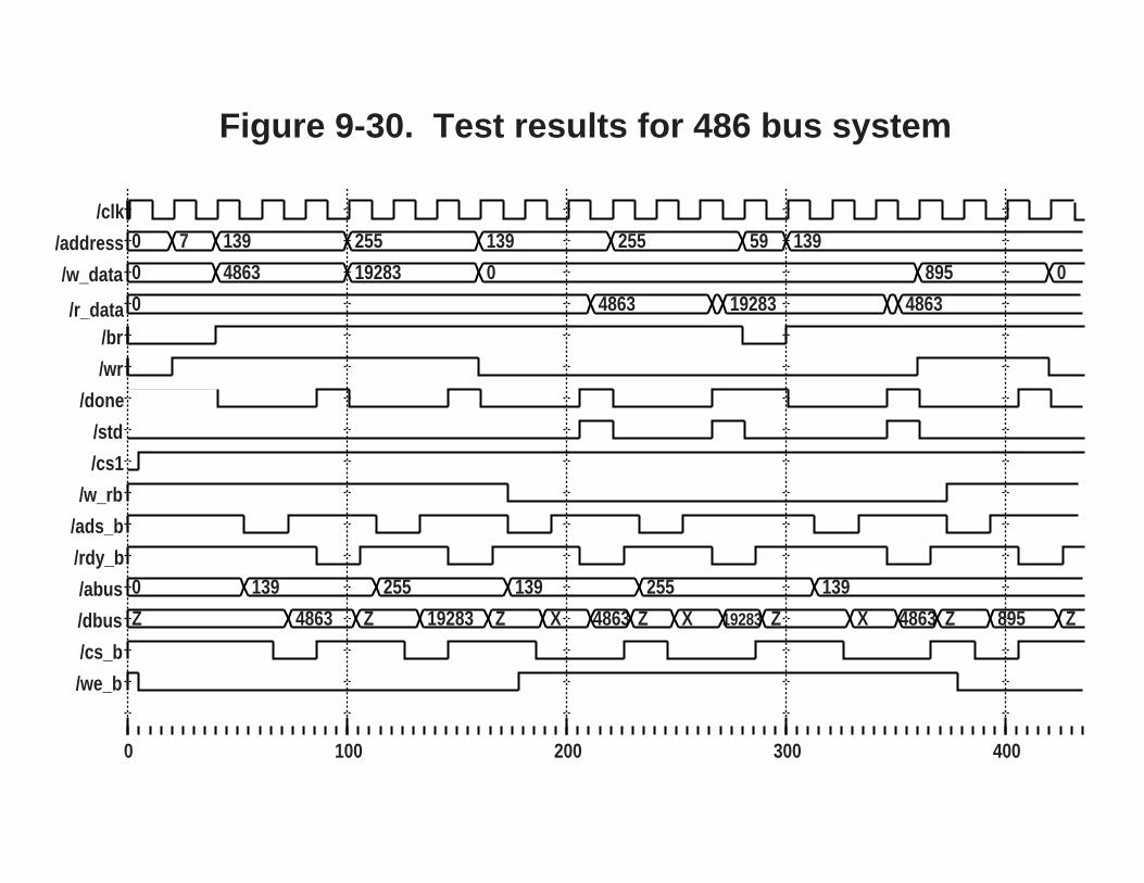
0 100 200 300 400
/clk
/address 0 7 139 255 139 255 59 139
/w_data 0 4863 19283 0 895 0
/r_data 0 4863 19283 4863
/br
/wr
/done
/std
/cs1
/w_rb
/ads_b
/rdy_b
/abus 0 139 255 139 255 139
/dbus Z 4863 Z 19283 Z X 4863 Z X 19283 Z X 4863 Z 895 Z
/cs_b
/we_b
Figure 9-30. Test results for 486 bus system