final 16gb e-die nand flashn2k1.com/n2k1/nb7/pdf/k9gag08u0e.pdf · - 3 - table of contents...
TRANSCRIPT

- 1 -
K9GAG08U0E
Rev. 0.9.1,Mar. 2010
SAMSUNG ELECTRONICS RESERVES THE RIGHT TO CHANGE PRODUCTS, INFORMATION AND SPECIFICATIONS WITHOUT NOTICE.
Products and specifications discussed herein are for reference purposes only. All information discussed herein is provided on an "AS IS" basis, without warranties of any kind.
This document and all information discussed herein remain the sole and exclusive property of Samsung Electronics. No license of any patent, copyright, mask work, trademark or any other intellectual property right is granted by one party to the other party under this document, by implication, estoppel or other-wise.
Samsung products are not intended for use in life support, critical care, medical, safety equipment, or similar applications where product failure could result in loss of life or personal or physical harm, or any military or defense application, or any governmental procurement to which special terms or provisions may apply.
For updates or additional information about Samsung products, contact your nearest Samsung office.
All brand names, trademarks and registered trademarks belong to their respective owners.
ⓒ 2010 Samsung Electronics Co., Ltd. All rights reserved.
K9LBG08U0EK9HCG08U1E
Final
16Gb E-die NAND FlashMulti-Level-Cell (2bit/cell)
datasheet

- 2 -
datasheet FLASH MEMORYRev. 0.9.1
K9LBG08U0E
FinalK9GAG08U0E
K9HCG08U1E
Revision History
Revision No. History Draft Date Remark Editor
0.0 1. Initial issue Jun. 12, 2009 Advance
0.1 1. Pin configuration is changed.2. tREA is changed from 20ns to 25ns.3. Memory cell array is amended.4. Row address is modified.5. Dummy busy time for Two-Plane Program(tDBSY) is deleted.
Oct. 21, 2009 Advance
0.2 1. Pin configuration is changed. Oct. 21, 2009 Advance
0.3 1. tRC/tWC is changed from 30ns to 20ns.2. The Parameter related tRC/tWC is changed
Nov. 6, 2009 Advance
0.4 1. 52LGA (11x14) QDP is added Nov. 13, 2009 Advance S.M.Lee
0.5 1. AC character‘s changed. Jan. 20, 2010 Advance S.M.Lee
0.9 1. Part ID K9LBG08U0E and K9HCG08U1E are added. Mar. 09, 2010 Final S.M.Lee
0.9.1 1. tR 300->400 changed.2. K9HCG08U5E is deleted.3.Package Dimensions of 48-TSOP are amended.
Mar. 31, 2010 Final S.M.Lee
- 3 -
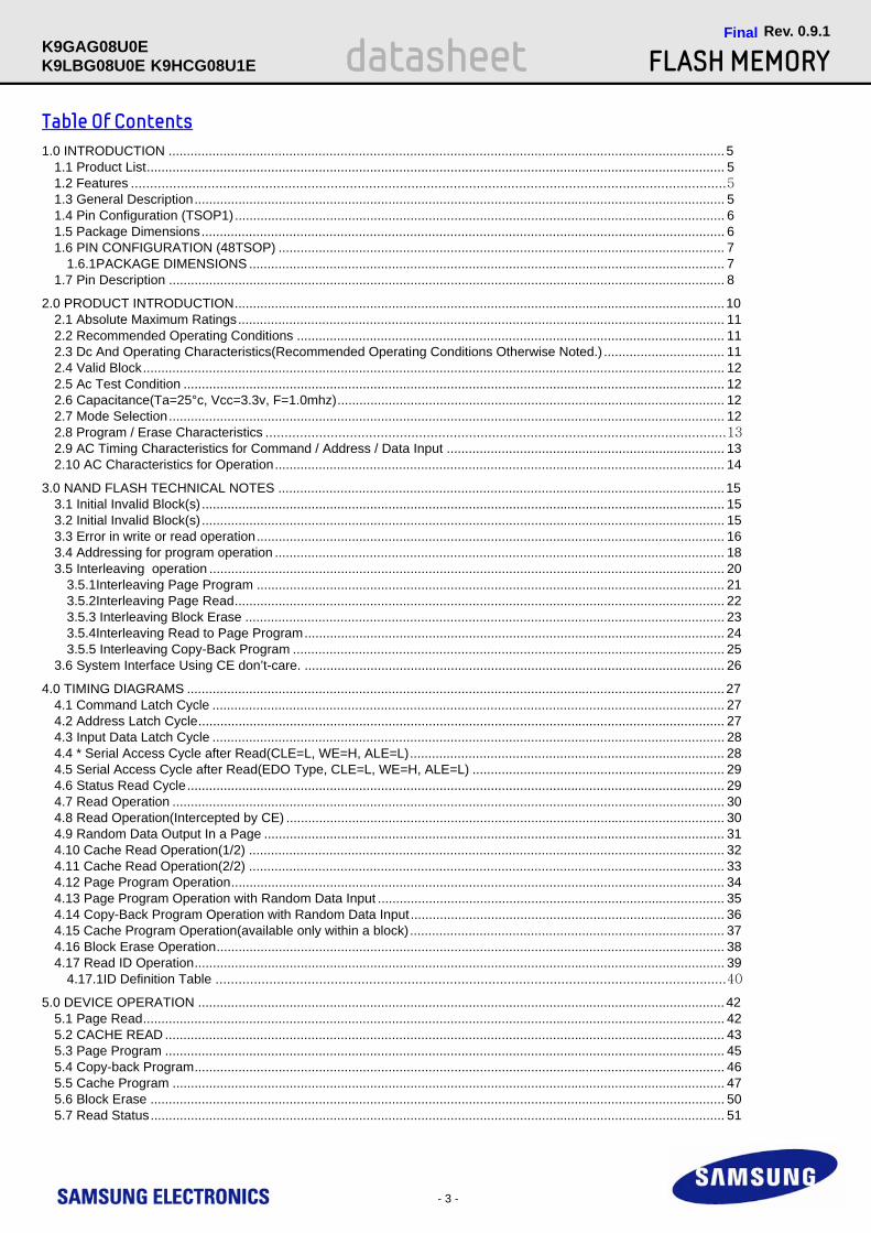
Table Of Contents
datasheet FLASH MEMORYRev. 0.9.1
K9LBG08U0E
FinalK9GAG08U0E
K9HCG08U1E
1.0 INTRODUCTION ........................................................................................................................................................ 51.1 Product List.............................................................................................................................................................. 51.2 Features ...........................................................................................................................................................51.3 General Description................................................................................................................................................. 51.4 Pin Configuration (TSOP1)...................................................................................................................................... 61.5 Package Dimensions............................................................................................................................................... 61.6 PIN CONFIGURATION (48TSOP) .......................................................................................................................... 7
1.6.1PACKAGE DIMENSIONS .................................................................................................................................. 71.7 Pin Description ........................................................................................................................................................ 8
2.0 PRODUCT INTRODUCTION......................................................................................................................................102.1 Absolute Maximum Ratings..................................................................................................................................... 112.2 Recommended Operating Conditions ..................................................................................................................... 112.3 Dc And Operating Characteristics(Recommended Operating Conditions Otherwise Noted.) ................................. 112.4 Valid Block............................................................................................................................................................... 122.5 Ac Test Condition .................................................................................................................................................... 122.6 Capacitance(Ta=25°c, Vcc=3.3v, F=1.0mhz).......................................................................................................... 122.7 Mode Selection........................................................................................................................................................ 122.8 Program / Erase Characteristics ........................................................................................................................132.9 AC Timing Characteristics for Command / Address / Data Input ............................................................................ 132.10 AC Characteristics for Operation........................................................................................................................... 14
3.0 NAND FLASH TECHNICAL NOTES .......................................................................................................................... 153.1 Initial Invalid Block(s) ............................................................................................................................................... 153.2 Initial Invalid Block(s) ............................................................................................................................................... 153.3 Error in write or read operation................................................................................................................................ 163.4 Addressing for program operation ........................................................................................................................... 183.5 Interleaving operation ............................................................................................................................................. 20
3.5.1Interleaving Page Program ................................................................................................................................ 213.5.2Interleaving Page Read...................................................................................................................................... 223.5.3 Interleaving Block Erase ................................................................................................................................... 233.5.4Interleaving Read to Page Program................................................................................................................... 243.5.5 Interleaving Copy-Back Program ...................................................................................................................... 25
3.6 System Interface Using CE don’t-care. ................................................................................................................... 26
4.0 TIMING DIAGRAMS ................................................................................................................................................... 274.1 Command Latch Cycle ............................................................................................................................................ 274.2 Address Latch Cycle................................................................................................................................................ 274.3 Input Data Latch Cycle ............................................................................................................................................ 284.4 * Serial Access Cycle after Read(CLE=L, WE=H, ALE=L)...................................................................................... 284.5 Serial Access Cycle after Read(EDO Type, CLE=L, WE=H, ALE=L) ..................................................................... 294.6 Status Read Cycle................................................................................................................................................... 294.7 Read Operation ....................................................................................................................................................... 304.8 Read Operation(Intercepted by CE) ........................................................................................................................ 304.9 Random Data Output In a Page .............................................................................................................................. 314.10 Cache Read Operation(1/2) .................................................................................................................................. 324.11 Cache Read Operation(2/2) .................................................................................................................................. 334.12 Page Program Operation....................................................................................................................................... 344.13 Page Program Operation with Random Data Input ............................................................................................... 354.14 Copy-Back Program Operation with Random Data Input ...................................................................................... 364.15 Cache Program Operation(available only within a block)...................................................................................... 374.16 Block Erase Operation........................................................................................................................................... 384.17 Read ID Operation................................................................................................................................................. 39
4.17.1ID Definition Table .....................................................................................................................................40
5.0 DEVICE OPERATION ................................................................................................................................................ 425.1 Page Read............................................................................................................................................................... 425.2 CACHE READ ......................................................................................................................................................... 435.3 Page Program ......................................................................................................................................................... 455.4 Copy-back Program................................................................................................................................................. 465.5 Cache Program ....................................................................................................................................................... 475.6 Block Erase ............................................................................................................................................................. 505.7 Read Status............................................................................................................................................................. 51

- 4 -
datasheet FLASH MEMORYRev. 0.9.1
K9LBG08U0E
FinalK9GAG08U0E
K9HCG08U1E
5.8 Read ID ................................................................................................................................................................... 525.9 RESET..................................................................................................................................................................... 525.10 Ready/Busy ........................................................................................................................................................... 53
6.0 DATA PROTECTION & POWER UP SEQUENCE.....................................................................................................546.1 WP AC Timing guide ............................................................................................................................................... 55

- 5 -
datasheet FLASH MEMORYRev. 0.9.1
K9LBG08U0E
FinalK9GAG08U0E
K9HCG08U1E
1.0 INTRODUCTION
1.1 Product List
1.2 Features• Voltage Supply - 3.3V Device : 2.7V ~ 3.6V• Organization - Memory Cell Array : (2,076M x 110.49K) x 8bit - Data Register : (8K + 436) x 8bit • Automatic Program and Erase - Page Program : (8K + 436)Byte - Block Erase : (1M + 54.5K)Byte• Page Read Operation - Page Size : (8K + 436)Byte - Random Read : 400μs(Max.) - Serial Access : 30ns(Min.)• Memory Cell : 2bit / Memory Cell• Fast Write Cycle Time - Program time : 1.2ms(Typ.) - Block Erase Time : 1.5ms(Typ.)
• Command/Address/Data Multiplexed I/O Port• Hardware Data Protection - Program/Erase Lockout During Power Transitions• Reliable CMOS Floating-Gate Technology - ECC Requirement : 24bit/(1K +54.5)Byte - Endurance & Data Retention : Pleae refer to the qualification report• Command Register Operation• Unique ID for Copyright Protection• Package : - K9GAG08U0E-SCB0/SIB0 : Pb-Halogen FREE PACKAGE 48 - Pin TSOP1 (12 x 20 / 0.5 mm pitch) - K9LBG08U0E-SCB0/SIB0 : Pb-Halogen FREE PACKAGE 48 - Pin TSOP1 (12 x 20 / 0.5 mm pitch) - K9HCG08U1E-SCB0/SIB0 : Pb-Halogen FREE PACKAGE 48 - Pin TSOP1 (12 x 20 / 0.5 mm pitch)
1.3 General DescriptionThe device is offered in 3.3V Vcc. Its NAND cell provides the most cost-effective solution for the solid state mass storage market. A program operation can be performed in typical 1.2ms on the 8,628-byte page and an erase operation can be performed in typical 1.5ms on a (1M+54.5K)byte block. Data in the data register can be read out at 30ns cycle time per byte. The I/O pins serve as the ports for address and data input/output as well as command input. The on-chip write controller automates all program and erase functions including pulse repetition, where required, and internal verification and margining of data. Even the write-intensive systems can take advantage of the K9GAG08U0E′s extended reliability of P/E cycles which are presented in the Qualifi-cation report by providing ECC(Error Correcting Code) with real time mapping-out algorithm. The K9GAG08U0E is an optimum solution for large nonvol-atile storage applications such as solid state file storage and other portable applications requiring non-volatility.
Part Number Density Interface Vcc Range Organization PKG Type
K9GAG08U0E-S 16GbConventional 2.7V ~ 3.6V x8 48TSOP1K9LBG08U0E-S 32Gb
K9HCG08U1E-S 64Gb

- 6 -
datasheet FLASH MEMORYRev. 0.9.1
K9LBG08U0E
FinalK9GAG08U0E
K9HCG08U1E
1.4 Pin Configuration (48TSOP)
K9GAG08U0E-SCB0/SIB0
48-pin TSOP1Standard Type12mm x 20mm
123456789101112131415161718192021222324
484746454443424140393837363534333231302928272625
N.CN.CN.CN.CN.CN.CR/B RECE
N.CN.CVccVssN.CN.CCLEALEWEWPN.CN.CN.CN.CN.C
N.CN.CN.CN.CI/O7I/O6I/O5I/O4N.CN.C
VccVssN.CN.CN.CI/O3I/O2I/O1I/O0N.CN.CN.CN.C
N.C
K9LBG08U0E-SCB0/SIB0
1.4.1 Package Dimensions
48-PIN LEAD FREE PLASTIC THIN SMALL OUT-LINE PACKAGE TYPE(I)
48 - TSOP1 - 1220AF Unit :mm
#1
#240.50
TYP
[0.5
0±0.
06]
#48
0.10
0.
075
MA
X
0.05 MIN
(18.80)(13°)
0.12
5+0
.075
-0.0
35
0.20
+0.0
7-0
.03
(1.0
0)
(1.00)
(1.0
0)
(1.00)
0.16
+0.0
3-0
.01
#25
(0.2
5)
18.40.±0.10
(19.00)
20.00.±0.20
0.43
75±0
.05
0.43
75±0
.05
(R0.1
5)
(R0.15)
(10°)
1.20MAX1.00.±0.05
(13°)(10°)
12.0
0.±0
.10
(R0.15)(R0.15)
0.45 ~ 0.75
(0.50)
0° ~ 8°
(R0.25)(R0.25)0.
25TY
P

- 7 -
datasheet FLASH MEMORYRev. 0.9.1
K9LBG08U0E
FinalK9GAG08U0E
K9HCG08U1E
1.5 Pin Configuration (48TSOP)
48-pin TSOP1Standard Type12mm x 20mm
123456789
101112131415161718192021222324
484746454443424140393837363534333231302928272625
N.CN.CN.CN.CN.C
R/B2R/B1
RECE1CE2N.CVccVssN.CN.CCLEALEWEWPN.CN.CN.CN.CN.C
N.CN.CN.CN.CI/O7I/O6I/O5I/O4N.CN.CN.CVccVssN.CN.CN.CI/O3I/O2I/O1I/O0N.CN.CN.CN.C
K9HCG08U1E-SCB0/SIB0
1.5.1 package dimensions48-PIN LEAD/LEAD FREE PLASTIC THIN SMALL OUT-LINE PACKAGE TYPE(I)
48 - TSOP1 - 1220BF Unit :mm
#1
#240.50
TYP
[0.5
0±0.
06]
#48
0.10
0.
075
MA
X
0.02 MIN
(18.80)(13°)
0.12
5+0
.075
-0.0
35
0.20
+0.0
7-0
.03
(1.0
0)
(1.00)
(1.0
0)
(1.00)
#25
(0.2
5)
18.40.±0.10
(19.00)
20.00.±0.20
0.46
25±0
.05
0.46
25±0
.05
(R0.1
5)
(R0.15)
(10°)
1.20MAX1.05.±0.3
(13°)(10°)
12.0
0.±0
.10
(R0.15)(R0.15)
0.45 ~ 0.75
(0.50)
0°~ 8°
(R0.25)(R0.25)0.
25TY
P
0.16
+0.0
7-0
.03
- 8 -
datasheet FLASH MEMORYRev. 0.9.1
K9LBG08U0E
FinalK9GAG08U0E
K9HCG08U1E
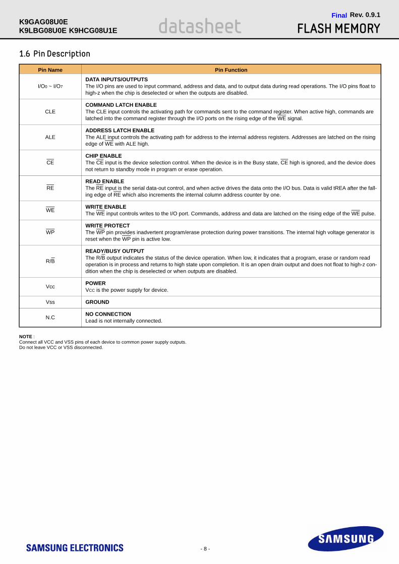
1.6 Pin Description
NOTE :Connect all VCC and VSS pins of each device to common power supply outputs.Do not leave VCC or VSS disconnected.
Pin Name Pin Function
I/O0 ~ I/O7
DATA INPUTS/OUTPUTS The I/O pins are used to input command, address and data, and to output data during read operations. The I/O pins float to high-z when the chip is deselected or when the outputs are disabled.
CLECOMMAND LATCH ENABLEThe CLE input controls the activating path for commands sent to the command register. When active high, commands are latched into the command register through the I/O ports on the rising edge of the WE signal.
ALEADDRESS LATCH ENABLEThe ALE input controls the activating path for address to the internal address registers. Addresses are latched on the rising edge of WE with ALE high.
CECHIP ENABLEThe CE input is the device selection control. When the device is in the Busy state, CE high is ignored, and the device does not return to standby mode in program or erase operation.
REREAD ENABLEThe RE input is the serial data-out control, and when active drives the data onto the I/O bus. Data is valid tREA after the fall-ing edge of RE which also increments the internal column address counter by one.
WE WRITE ENABLEThe WE input controls writes to the I/O port. Commands, address and data are latched on the rising edge of the WE pulse.
WPWRITE PROTECTThe WP pin provides inadvertent program/erase protection during power transitions. The internal high voltage generator is reset when the WP pin is active low.
R/B
READY/BUSY OUTPUTThe R/B output indicates the status of the device operation. When low, it indicates that a program, erase or random read operation is in process and returns to high state upon completion. It is an open drain output and does not float to high-z con-dition when the chip is deselected or when outputs are disabled.
Vcc POWERVCC is the power supply for device.
Vss GROUND
N.C NO CONNECTIONLead is not internally connected.

VCC
X-Buffers
Command
I/O Buffers & Latches
Latches& Decoders
Y-BuffersLatches& Decoders
Register
Control Logic& High Voltage
Generator Global Buffers OutputDriver
VSS
A14 - A33
A0 - A13
Command
CEREWE
CLE WP
I/0 0
I/0 7
VCCVSS
ALE
(16,608M + 883.9M)BitsNAND Flash
ARRAY
(8,192 + 436)Byte x 265,728
Y-Gating
Data Register & S/A
Figure 1. K9GAG08U0E Functional Block Diagram
Figure 2. K9GAG08U0E Array Organization
8K Bytes 436 Bytes
(=2,076 Blocks)
8K Bytes
8 bit
436 Bytes
1 Block = 128 Pages(1M + 54.5K)Bytes
I/O 0 ~ I/O 7
1 Page = (8K + 436)Bytes1 Block = (8K + 436)B x 128 Pages = (1M + 54.5K) Bytes
= 17,491 Mbits
Page Register
265,728 Pages
- 9 -
datasheet FLASH MEMORYRev. 0.9.1
K9LBG08U0E
FinalK9GAG08U0E
K9HCG08U1E
NOTE : Column Address : Starting Address of the Register.* L must be set to ’Low’.* The device ignores any additional input of address cycles than required.* Row Address consists of Page address (A14 ~ A20) & Block address(A21 ~ the last Address)
I/O 0 I/O 1 I/O 2 I/O 3 I/O 4 I/O 5 I/O 6 I/O 7
1st Cycle A0 A1 A2 A3 A4 A5 A6 A7
2nd Cycle A8 A9 A10 A11 A12 A13 *L *L
3rd Cycle A14 A15 A16 A17 A18 A19 A20 A21
4th Cycle A22 A23 A24 A25 A26 A27 A28 A29
5th Cycle A30 A31 A32 A33* *L *L *L *L
Row Address;
Column Address
Block Address : A21 ~ A32Page Address : A14 ~ A20
*A33 : Chip address forK9LBG08U0E, K9HCG08U1E

- 10 -
datasheet FLASH MEMORYRev. 0.9.1
K9LBG08U0E
FinalK9GAG08U0E
K9HCG08U1E
2.0 PRODUCT INTRODUCTIONNAND Flash Memory has addresses multiplexed into 8 I/Os. This scheme dramatically reduces pin counts and allows system upgrades to future densities by maintaining consistency in system board design. Command, address and data are all written through I/O's by bringing WE to low while CE is low. Those are latched on the rising edge of WE. Command Latch Enable(CLE) and Address Latch Enable(ALE) are used to multiplex command and address respectively, via the I/O pins. Some commands require one bus cycle. For example, Reset Command, Status Read Command, etc. require just one cycle bus. Some other commands, like page read and block erase and page program, require two cycles: one cycle for setup and the other cycle for execution..Page Read and Page Program need the same five address cycles following the required command input. In Block Erase operation, however, only the three row address cycles are used. Device operations are selected by writing specific commands into the command register. The table below defines the specific commands.
[Table 1] Command Sets
NOTE : 1) Random Data Input/Output can be executed in a page.
CAUTION : Any undefined command inputs are prohibited except for above command set of Table 1.
Function 1st Set 2nd Set Acceptable Command during Busy
Read 00h 30h
Read for Copy Back 00h 35h
Cache Read 31h -
Read Start for Last Page Cache Read 3Fh -
Page Program 80h 10h
Cache Program 80h 15h
Copy-Back Program 85h 10h
Block Erase 60h D0h
Random Data Input(1) 85h -
Random Data Output(1) 05h E0h
Read ID 90h -
Read Status 70h - O
Chip Status1 F1h - O
Chip Status2 F2h O
Reset FFh - O

- 11 -
datasheet FLASH MEMORYRev. 0.9.1
K9LBG08U0E
FinalK9GAG08U0E
K9HCG08U1E
2.1 Absolute Maximum Ratings
NOTE : 1) Minimum DC voltage is -0.6V on input/output pins. During transitions, this level may undershoot to -2.0V for periods <30ns. Maximum DC voltage on input/output pins is VCC+0.3V which, during transitions, may overshoot to VCC+2.0V for periods <20ns.2) Permanent device damage may occur if ABSOLUTE MAXIMUM RATINGS are exceeded. Functional operation should be restricted to the conditions as detailed in the operational sections of this data sheet. Exposure to absolute maximum rating conditions for extended periods may affect reliability.
2.2 Recommended Operating Conditions(Voltage reference to GND, K9XXG08XXE-XCB0 :TA=0 to 70°C(1), K9XXG08XXE-XIB0:TA=-40 to 85°C(1))
NOTE: 1) Data retention is not guaranteed on Operating condition temperature over/under.
2.3 Dc And Operating Characteristics(Recommended Operating Conditions Otherwise Noted.)
NOTE : 1) VIL can undershoot to -0.4V and VIH can overshoot to VCC +0.4V for durations of 20 ns or less.2) Typical value is measured at Vcc=3.3V, TA=25°C. Not 100% tested.3) The Typical value of the K9LBG08U0E’s ISB is 20μA and the maximum value is100μA The Typical value of the K9HCG08U1E’s ISB is 40μA and the maximum value is200μA4) The Typical value of K9LBG08U0E, K9HCG08U1E’s Icc1, Icc2 and Icc3 are 35mA and the maximum values are 55mA.5) The maximum value of K9LBG08U0E’s is ±20μA. The maximum value of K9HCG08U1E’s is ±40μA.
Parameter Symbol Rating Unit
Voltage on any pin relative to VSS
VCC -0.6 to + 4.6
VVIN -0.6 to + 4.6
VI/O -0.6 to Vcc+0.3 (<4.6V)
Storage TemperatureK9XXG08UXE-XCB0
TSTG -65 to +100 °CK9XXG08UXE-XIB0
Short Circuit Current Ios 5 mA
Parameter Symbol Min Typ. Max Unit
Supply Voltage VCC 2.7 3.3 3.6 V
Supply Voltage VSS 0 0 0 V
Parameter Symbol Test Conditions Min Typ Max Unit
Operating Current
Page Read with Serial Access ICC1(4) tRC=30ns
CE=VIL, IOUT=0mA- 30 50 mAProgram ICC2(4) -
Erase ICC3(4) -
Stand-by Current(CMOS) ISB(3) CE=VCC-0.2, WP=0V/VCC - 10 50
μAInput Leakage Current ILI(5) VIN=0 to Vcc(max) - - ±10
Output Leakage Current ILO(5) VOUT=0 to Vcc(max) - - ±10
Input High Voltage VIH(1) - 0.8 xVcc - Vcc +0.3
VInput Low Voltage, All inputs VIL(1) - -0.3 - 0.2 xVcc
Output High Voltage Level VOH K9GAG08U0E :IOH=-400μA 2.4 - -
Output Low Voltage Level VOL K9GAG08U0E :IOL=2.1mA - - 0.4
Output Low Current(R/B) IOL(R/B) K9GAG08U0E :VOL=0.4V 8 10 - mA

- 12 -
datasheet FLASH MEMORYRev. 0.9.1
K9LBG08U0E
FinalK9GAG08U0E
K9HCG08U1E
2.4 Valid Block
NOTE : 1) The device may include initial invalid blocks when first shipped. Additional invalid blocks may develop while being used. The number of valid blocks is presented with both
cases of invalid blocks considered. Invalid blocks are defined as blocks that contain one or more bad bits which cause status failure during program and erase operation. Do not erase or program factory-marked bad blocks. Refer to the attached technical notes for appropriate management of invalid blocks.
2) The 1st block, which is placed on 00h block address, is guaranteed to be a valid block at the time of shipment
2.5 Ac Test Condition(K9XXG08XXE-XCB0 :TA=0 to 70°C, K9XXG08XXE-XIB0:TA=-40 to 85°C, K9XXG08UXE: Vcc=2.7V ~ 3.3V,unless otherwise noted)
2.6 Capacitance(Ta=25°c, Vcc=3.3v, F=1.0mhz)
NOTE :1) Capacitance is periodically sampled and not 100% tested.2) CI/O(W) and CIN(W) are tested at wafer level.
2.7 Mode Selection
NOTE :1) X can be VIL or VIH.
2) WP should be biased to CMOS high or CMOS low for standby.
Parameter Symbol Min Typ. Max Unit
K9GAG08U0ENVB
2,018-
2,076BlocksK9LBG08U0E 4,036 4,152
K9HCG08U1E 8,072 8,304
Parameter K9XXG08UXE
Input Pulse Levels 0V to Vcc
Input Rise and Fall Times 5ns
Input and Output Timing Levels Vcc/2
Output Load 1 TTL GATE and CL=50pF
Item Symbol Test ConditionK9GAG08U0E K9LBG08U0E K9HCG08U1E
UnitMin Max Min Max Min Max
Input/Output CapacitanceCI/O
VIL=0V- 8 - 13 - 23 pF
CI/O(W)* - 5 - 10 - 20 pF
Input CapacitanceCIN
VIN=0V- 8 - 13 - 23 pF
CIN(W)* - 5 - 10 - 20 pF
CLE ALE CE WE RE WP Mode
H L L H X Read Mode Command Input
L H L H X Address Input(5clock)
H L L H H Write Mode Command Input
L H L H H Address Input(5clock)
L L L H H Data Input
L L L H X Data Output
X X X X H X During Read(Busy)
X X X X X H During Program(Busy)
X X X X X H During Erase(Busy)
X X(1) X X X L Write Protect
X X H X X 0V/VCC(2) Stand-by

- 13 -
datasheet FLASH MEMORYRev. 0.9.1
K9LBG08U0E
FinalK9GAG08U0E
K9HCG08U1E
2.8 Program / Erase Characteristics
NOTE: 1)Typical program time is measured at Vcc=3.3V, TA=25°C. Not 100% tested.2) Typical Program time is defined as the time within which more than 50% of the whole pages are programed at 3.3V Vcc and 25°C temperature.3) Within a same block, program time(tPROG) of page group A is faster than that of page group B. Typical tPROG is the average program time of the page group A and B(Table 5). Page Group A: Page 0, 1, 3, 5, 7, ... , 77,79,7B,7D Page Group B: Page 2, 4, 6, 8, 0A, ... , 7A,7C,7E,7F4) tCBSY depends on the timing between internal programming time and data in time.
2.9 AC Timing Characteristics for Command / Address / Data Input
NOTES : 1. The transition of the corresponding control pins must occur only once while WE is held low 2. tADL is the time from the WE rising edge of final address cycle to the WE rising edge of first data cycle
Parameter Symbol Min Typ Max Unit
Program Time tPROG - 1.2 5 ms
Dummy Busy Time for Cache Program tCBSY(4) - - 5 ms
Number of Partial Program Cycles in the Same Page Nop - - 1 cycle
Block Erase Time tBERS - 1.5 10 ms
Parameter Symbol Min Max Unit
CLE Setup Time tCLS(1) 15 - ns
CLE Hold Time tCLH 5 - ns
CE Setup Time tCS(1) 25 - ns
CE Hold Time tCH 5 - ns
WE Pulse Width tWP 15 - ns
ALE Setup Time tALS(1) 15 - ns
ALE Hold Time tALH 5 - ns
Data Setup Time tDS(1) 15 - ns
Data Hold Time tDH 5 - ns
Write Cycle Time tWC 30 - ns
WE High Hold Time tWH 10 - ns
Address to Data Loading Time tADL(2) 300 - ns

- 14 -
datasheet FLASH MEMORYRev. 0.9.1
K9LBG08U0E
FinalK9GAG08U0E
K9HCG08U1E
2.10 AC Characteristics for Operation
Note :1) If reset command(FFh) is written at Ready state, the device goes into Busy for maxium 10us.
Parameter Symbol Min Max Unit
Data Transfer from Cell to Register tR - 400 μs
ALE to RE Delay tAR 10 - ns
CLE to RE Delay tCLR 10 - ns
Ready to RE Low tRR 20 - ns
RE Pulse Width tRP 15 - ns
WE High to Busy tWB - 100 ns
WP High to WE Low tWW 100 ns
Read Cycle Time tRC 30 - ns
RE Access Time tREA - 25 ns
CE Access Time tCEA - 35 ns
RE High to Output Hi-Z tRHZ - 100 ns
CE High to Output Hi-Z tCHZ - 30 ns
CE High to ALE or CLE Don’t Care tCSD 0 - ns
RE High to Output Hold tRHOH 15 - ns
RE Low to Output Hold tRLOH 5 - ns
RE High Hold Time tREH 10 - ns
Output Hi-Z to RE Low tIR 0 - ns
RE High to WE Low tRHW 100 - ns
WE High to RE Low tWHR 60 - ns
Device Resetting Time(Read/Program/Erase) tRST - 10/30/500(1) μs
Cache Busy in Read Cache (following 31h and 3Fh) tDCBSYR - 400 μs

- 15 -
datasheet FLASH MEMORYRev. 0.9.1
K9LBG08U0E
FinalK9GAG08U0E
K9HCG08U1E
3.0 NAND FLASH TECHNICAL NOTES
3.1 Initial Invalid Block(s)Initial invalid blocks are defined as blocks that contain one or more initial invalid bits whose reliability is not guaranteed by Samsung. The information regarding the initial invalid block(s) is called the initial invalid block information. Devices with initial invalid block(s) have the same quality level as devices with all valid blocks and have the same AC and DC characteristics. An initial invalid block(s) does not affect the performance of valid block(s) because it is isolated from the bit line and the common source line by a select transistor. The system design must be able to mask out the initial invalid block(s) via address mapping. The 1st block, which is placed on 00h block address, is guaranteed to be a valid block at the time of shipment.
3.2 Initial Invalid Block(s)All device locations are erased(FFh) except locations where the initial invalid block(s) information is written prior to shipping. The initial invalid block(s) status is defined by the 1st byte in the spare area. Samsung makes sure that the first or the last page of every initial invalid block has non-FFh data at the column address of 0 or 8,192.The initial invalid block information is also erasable in most cases, and it is impossible to recover the information once it has been erased. Therefore, the system must be able to recognize the initial invalid block(s) based on the initial invalid block information and create the initial invalid block table via the following suggested flow chart. Any intentional erasure of the initial invalid block information is prohibited
Figure 3. Flow Chart to Create Initial Invalid Block Table
No
Yes
Read FFh CheckColumn 0 or 8192of the last page
Block No = 1
End
Pass
Pass
Fail
Start
Block No. = Block No. + 1
Read FFh CheckColumn 0 or 8192of the First page
Entry Bad Block 1)
Fail
Last Block
NOTE :1) No Erase Operation is allowed to detected bad block

- 16 -
datasheet FLASH MEMORYRev. 0.9.1
K9LBG08U0E
FinalK9GAG08U0E
K9HCG08U1E
3.3 Error in write or read operationWithin its life time, additional invalid blocks may develop with NAND Flash memory. Refer to the qualification report for the actual data. Block replacement should be done upon erase or program error.
ECC : Error Correcting Code --> RS Code or BCH Code etc. Example) 24bit correction / 1K+54.5 byte
Program Flow Chart
Start
I/O 6 = 1 ?
I/O 0 = 0 ? No*
Write 80h
Write Address
Write Data
Write 10h
Read Status Register
Program Completed
or R/B = 1 ?
Program Error
Yes
No
Yes
: If program operation results in an error, map outthe block including the page in error and copy the *target data to another block.
Failure Mode Detection and Countermeasure sequence
Write Erase Failure Status Read after Erase --> Block Replacement
Program Failure Status Read after Program --> Block Replacement
Read Up to 24 Bit Failure Verify ECC -> ECC Correction

- 17 -
datasheet FLASH MEMORYRev. 0.9.1
K9LBG08U0E
FinalK9GAG08U0E
K9HCG08U1E
NAND Flash Technical Notes (Continued)
Erase Flow Chart
Start
I/O 6 = 1 ?
I/O 0 = 0 ? No*
Write 60h
Write Block Address
Write D0h
Read Status Register
or R/B = 1 ?
Erase Error
Yes
No
: If erase operation results in an error, map outthe failing block and replace it with another block. *
Erase Completed
Yes
Read Flow Chart
Start
Verify ECC No
Write 00h
Write Address
Read Data
ECC Generation
Reclaim the Error
Page Read Completed
Yes
Write 30h
Block Replacement
Buffer memory of the controller.
1stBlock A
Block B
(n-1)thnth
(page)
{∼
1st
(n-1)thnth
(page)
{∼
an error occurs.1
2
* Step1When an error happens in the nth page of the Block ’A’ during erase or program operation. * Step2Copy the data in the 1st ~ (n-1)th page to the same location of another free block. (Block ’B’)* Step3Then, copy the nth page data of the Block ’A’ in the buffer memory to the nth page of the Block ’B’.* Step4Do not erase or program Block ’A’ by creating an ’invalid block’ table or other appropriate scheme.

- 18 -
datasheet FLASH MEMORYRev. 0.9.1
K9LBG08U0E
FinalK9GAG08U0E
K9HCG08U1E
3.4 Addressing for program operationWithin a block, the pages must be programmed consecutively from the LSB (least significant bit) page of the block to MSB (most significant bit) pages of the block. Random page address programming is prohibited. In this case, the definition of LSB page is the LSB among the pages to be programmed. Therefore, LSB doesn’t need to be page 0.
From the LSB page to MSB page
DATA IN: Data (1) Data (128)
(1)(2)(3)
(32)
(128)
Data register
Page 0Page 1Page 2
Page 31
Page 127
Ex.) Random page program (Prohibition)
DATA IN: Data (1) Data (128)
(2)(32)(3)
(1)
(128)
Data register
Page 0Page 1Page 2
Page 31
Page 127
:
:
:
:
- 19 -
datasheet FLASH MEMORYRev. 0.9.1
K9LBG08U0E
FinalK9GAG08U0E
K9HCG08U1E
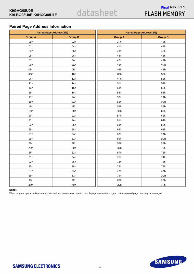
Paired Page Address Information
NOTE :When program operation is abnormally aborted (ex. power-down, reset), not only page data under program but also paired page data may be damaged.
Paired Page Address(1/2) Paired Page Address(2/2)
Group A Group B Group A Group B
00h 02h 3Fh 42h
01h 04h 41h 44h
03h 06h 43h 46h
05h 08h 45h 48h
07h 0Ah 47h 4Ah
09h 0Ch 49h 4Ch
0Bh 0Eh 4Bh 4Eh
0Dh 10h 4Dh 50h
0Fh 12h 4Fh 52h
11h 14h 51h 54h
13h 16h 53h 56h
15h 18h 55h 58h
17h 1Ah 57h 5Ah
19h 1Ch 59h 5Ch
1Bh 1Eh 5Bh 5Eh
1Dh 20h 5Dh 60h
1Fh 22h 5Fh 62h
21h 24h 61h 64h
23h 26h 63h 66h
25h 28h 65h 68h
27h 2Ah 67h 6Ah
29h 2Ch 69h 6Ch
2Bh 2Eh 6Bh 6Eh
2Dh 30h 6Dh 70h
2Fh 32h 6Fh 72h
31h 34h 71h 74h
33h 36h 73h 76h
35h 38h 75h 78h
37h 3Ah 77h 7Ah
39h 3Ch 79h 7Ch
3Bh 3Eh 7Bh 7Eh
3Dh 40h 7Dh 7Fh

- 20 -
datasheet FLASH MEMORYRev. 0.9.1
K9LBG08U0E
FinalK9GAG08U0E
K9HCG08U1E
3.5 Interleaving operationK9LBG08U0E and K9HCG08U1E devices are composed of two chips sharing per CE pin. They provide interleaving operation between two chipsThis interleaving operation improves the system throughput almost twice compared to non-interleaving operation.
At first, the host issues a operation command to one of the LSB chips, say (chip #1). Due to DDP device goes into busy state. During this time, MSB chip (chip #2) is in ready state. So it can execute the operation command issued by the host.
After the execution of operation by LSB chip (chip #1), it can execute another operation regardless of MSB chip (chip #2). Before that the host needs to check the status of LSB chip (chip #1) by issuing F1h command. Only when the status of LSB chip (chip #1) becomes ready status, host can issue another operation command. If LSB chip (chip #1) is in busy state, the host has to wait for LSB chip (chip #1) to get into ready state.
Similarly, MSB chip (chip #2) can execute another operation after the completion of the previous operation. The host can monitor the status of MSB chip (chip #2) by issuing F2h command. When MSB chip (chip #2) shows ready state, host can issue another operation command to MSB chip (chip #2).
This interleaving algorithm improves the system throughput almost twice. The host can issue page operation command to each chip individually. This reduces the time lag for the completion of operation.
NOTES : During interleave operations, 70h command is prohibited.
[Table 2] F1h Read Status Register Definition
NOTE : 1. I/Os defined ’Not use’ are recommended to be masked out when Read Status is being executed.
[Table 3] F2h Read Status Register Definition
NOTE : 1. I/Os defined ’Not use’ are recommended to be masked out when Read Status is being executed.
I/O No. Page Program Block Erase Read Definition
I/O 0 Chip1 Pass/Fail Chip1 Pass/Fail Not use Pass : "0" Fail : "1"
I/O 1 Plane Pass/Fail Plane Pass/Fail Not use Pass : "0" Fail : "1"
I/O 2 Not Use Not Use Not use Don’t -cared
I/O 3 Not Use Not Use Not Use Don’t -cared
I/O 4 Not Use Not Use Not Use Don’t -cared
I/O 5 Not Use Not Use Not Use Don’t -cared
I/O 6 Ready/Busy Ready/Busy Ready/Busy Busy : "0" Ready : "1"
I/O 7 Write Protect Write Protect Write Protect Protected : "0" Not Protected : "1"
I/O No. Page Program Block Erase Read Definition
I/O 0 Chip2 Pass/Fail Chip2 Pass/Fail Not use Pass : "0" Fail : "1"
I/O 1 Plane Pass/Fail Plane Pass/Fail Not use Pass : "0" Fail : "1"
I/O 2 Not Use Not Use Not use Don’t -cared
I/O 3 Not Use Not Use Not Use Don’t -cared
I/O 4 Not Use Not Use Not Use Don’t -cared
I/O 5 Not Use Not Use Not Use Don’t -cared
I/O 6 Ready/Busy Ready/Busy Ready/Busy Busy : "0" Ready : "1"
I/O 7 Write Protect Write Protect Write Protect Protected : "0" Not Protected : "1"

- 21 -
datasheet FLASH MEMORYRev. 0.9.1
K9LBG08U0E
FinalK9GAG08U0E
K9HCG08U1E
3.5.1 Interleaving Page Program
R/B (#1) busy of Chip #1
I/OX80h 10h
Chip Address : Low
Add & Data 80h 10h
Chip Address : High
Add & Data
busy of Chip #2
internal only
internal only
R/B
≈≈
≈
A B
R/B (#2)
1
busy of Chip #1
F1h
busy of Chip #2
≈≈
≈
B C D
another page program on Chip #1
I/O6Ready
Busy
"1"
"0"
1
R/B (#1)
I/OX
internal only
internal only
R/B
R/B (#2)
F2h I/O6Ready
Busy
"1"
"0"
State A : Chip #1 is executing page program operation and chip #2 is in ready state. So the host can issue page program command to chip #2.State B : Both chip #1 and chip #2 are executing page program operation.State C : Page program on chip #1 is terminated, but page program on chip #2 is still operating. And the system should issue F1h /F2hcommand to detect the status of chip #1. If chip #1 is ready, status I/O6 is "1" and the system can issue another page program command to chip #1.State D : Chip #1 and Chip #2 are ready.
According to the above process, the system can operate page program on chip #1 and chip #2 alternately.
- 22 -
datasheet FLASH MEMORYRev. 0.9.1
K9LBG08U0E
FinalK9GAG08U0E
K9HCG08U1E
3.5.2 Interleaving Page Read
Add00h 30h 00h 30h F1h
Chip Address: Low Chip Address: High
Add I/O6Ready
Busy
"1"
"0"
A B C 1
R/B (#1)
I/OX
internal only
R/B (#2)internal only
R/B
Add00h 05h
Chip Address: Low
Add E0h
Column Address
D
R/B (#1)
I/OX
internal only
R/B (#2)internal only
R/B
Data Out Add00h
1
Add 05h Col.Add E0h Data Out
E
R/B (#1)
I/OX
internal only
R/B (#2)internal only
R/B
2
2
F2h I/O6Ready
Busy
"1"
"0"
State A : Chip #1 is executing page read operation, and chip #2 is in ready state. So the host can issue page read command to chip #2.State B : Both chip #1 and chip #2 are executing page read operation.State C : Page read on chip #1 is completed and chip #2 is still executing page read operation.State D : Before the host read the data, the host should check the Ready/Busy status for both chips by F1h and F2h commands.State E : Chip #1 and Chip #2 are ready.Note : *F1h command is required to check the status of chip #1. F2h command is required to check the status of chip #2.

- 23 -
datasheet FLASH MEMORYRev. 0.9.1
K9LBG08U0E
FinalK9GAG08U0E
K9HCG08U1E
3.5.3 Interleaving Block Erase
R/B (#1) busy of Chip #1
I/OX60h D0h
Chip Address : Low
Add 60h D0h
Chip Address : High
Add
internal only
R/B (#2)internal only
≈≈
≈
A B
R/B
1
F1h
busy of Chip #2
≈≈
≈
B C D
another block erase on Chip #1
I/O6Ready
Busy
"1"
"0"
R/B (#1)
I/OX
internal only
R/B (#2)internal only
R/B
1
F2h I/O6Ready
Busy
"1"
"0"
State A : Chip #1 is executing block erase operation, and chip #2 is in ready state. So the host can issue block erase command to chip #2.State B : Both chip #1 and chip #2 are executing block erase operation.State C : Block erase on chip #1 is terminated, but block erase on chip #2 is still operating. And the system should issue F1h /F2hcommand to detect the status of chip #1. If chip #1 is ready, status I/O6 is "1" and the system can issue another block erase command to chip #1.State D : Chip #1 and Chip #2 are ready.
According to the above process, the system can operate block erase on chip #1 and chip #2 alternately.

- 24 -
datasheet FLASH MEMORYRev. 0.9.1
K9LBG08U0E
FinalK9GAG08U0E
K9HCG08U1E
3.5.4 Interleaving Read to Page Program
R/B (#1)
I/OX
internal only
R/B (#2)internal only
R/B
A B
10h80h
Chip Address : Low
Add Data in
tPROG of chip #1
tR of chip #2
30h00h Add
Chip Address : High
F2h
1
R/B (#1)
I/OX
internal only
R/B (#2)internal only
R/B C
05h00h
Chip Address : High
Add Data out
tPROG of chip #1
Add E0h
Column Address
F1h I/O6Ready
Busy
"1"
"0"
D
I/O6Ready
Busy
"1"
"0"
1
State A : Chip #1 is executing page program operation, and chip #2 is in ready state. So the host can issue read command to chip #2.State B : Both chip #1 is executing page program operation and chip #2 is executing read operation.State C : Read operation on chip #2 is completed and chip #2 is ready for the next operation. Chip #1 is still executing page program operation.State D : Both chip #1 and chip #2 are ready.Note : *F1h command is required to check the status of chip #1 to issue the next command to chip #1. F2h command is required to check the status of chip #2 to issue the next command to chip #2.As the above process, the system can operate Interleave read to page porgram on chip #1 and chip #2 alternatively.

- 25 -
datasheet FLASH MEMORYRev. 0.9.1
K9LBG08U0E
FinalK9GAG08U0E
K9HCG08U1E
3.5.5 Interleaving Copy-Back Program
R/B (#1)
I/OX
internal only
R/B (#2)internal only
R/B
35h00h
Chip Address : Low
Add I/O6Ready
Busy
"1"
"0"
F1h 05h00h Add E0hAdd
Chip Address : Low Column Address
tR of chip #1
1
I/OX
R/B
1 B C
tPROG of chip #1
A
10h85h
Chip Address : Low
Add & Data 35h00h
Chip Address : High
Add
tR of chip #2
I/O6Ready
Busy
"1"
"0"
R/B (#1)internal only
R/B (#2)internal only
2
00h
R/B (#1)
I/OX
internal only
R/B (#2)internal only
R/B
2
10h85h
Chip Address : High
Add & Data Data Out
D
05hAdd E0hAdd
Column AddressChip Address : High
3
E
tPROG of chip #2
I/O6Ready
Busy
"1"
"0"
F
R/B (#1)
I/OX
internal only
R/B (#2)internal only
R/B
3
F2h
F1h
F1h I/O6Ready
Busy
"1"
"0"
F2h
State A : Chip #1 is executing copy-back program operation, and chip #2 is in ready state. So the host can issue read for copy-back command to chip #2.State B : Chip #1 is executing copy-back program operation and chip #2 is executing read for copy-back operation.State C : Read for copy-back operation on chip #2 is completed and chip #2 is ready for the next operation. Chip #1 is still executing copy-back program operation.State D : Both chip #1 and chip #2 are executing copy-back program operation.State E : Chip #2 is still executing a copy-back program operation, and chip #1 is in ready for the next operation. State F : Both chip #1 and chip #2 are ready.Note : *F1h command is required to check the status of chip #1 to issue the next command to chip #1. F2h command is required to check the status of chip #2 to issue the next command to chip #2.As the above process, the system can operate Interleave copy-back program on chip #1 and chip #2 alternatively.

- 26 -
datasheet FLASH MEMORYRev. 0.9.1
K9LBG08U0E
FinalK9GAG08U0E
K9HCG08U1E
3.6 System Interface Using CE don’t-care. For an easier system interface, CE may be inactive during the data-loading or serial access as shown below. The internal 8,628byte data registers are utilized as separate buffers for this operation and the system design gets more flexible. In addition, for voice or audio applications which use slow cycle time on the order of μ-seconds, de-activating CE during the data-loading and serial access would provide significant savings in power consumption.
Figure 4. Program Operation with CE don’t-care.
Figure 5. Read Operation with CE don’t-care.
Address(5Cycle)00h
CE
CLE
ALE
WE
Data Output(serial access)
CE don’t-care
R/B tR
RE
30hI/Ox
≈
≈≈
≈≈
≈
≈≈
≈≈
≈
≈
CE
WEtWP
tCHtCS
Address(5Cycles)80h Data Input
CE
CLE
ALE
WE
Data Input
CE don’t-care
10h
tCEA
out
tREA
CE
RE
I/O0~7
I/Ox
≈≈
≈≈
≈≈
≈≈
≈≈
≈ ≈

- 27 -
datasheet FLASH MEMORYRev. 0.9.1
K9LBG08U0E
FinalK9GAG08U0E
K9HCG08U1E
4.0 TIMING DIAGRAMS
4.1 Command Latch Cycle
CE
WE
CLE
ALE
Command
tCLS
tCS
tCLH
tCH
tWP
tALS tALH
tDS tDH
I/Ox
4.2 Address Latch Cycle
CE
WE
CLE
ALE
Col. Add1
tCStWC
tWP
tALS
tDStDH
tALH tALStWH
tWC
tWP
tDStDH
tALH tALStWH
tWC
tWP
tDStDH
tALH tALStWH
tDStDH
tWP
I/Ox Col. Add2 Row Add1 Row Add2
tWC
tWHtALH tALS
tDStDH
Row Add3
tALH
tCLS
- 28 -
datasheet FLASH MEMORYRev. 0.9.1
K9LBG08U0E
FinalK9GAG08U0E
K9HCG08U1E
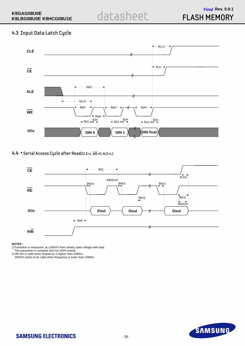
4.3 Input Data Latch Cycle
CE
CLE
WE
DIN 0 DIN 1 DIN final
ALE
tALS
tCLH
tWC
tCH
tDS tDH tDStDH
tDStDH
tWP
tWH
tWP tWP≈≈
≈I/Ox
≈≈
≈
4.4 * Serial Access Cycle after Read(CLE=L, WE=H, ALE=L)
RE
CE
R/B
Dout Dout Dout
tRC
tREA
tRR
tRHOH
tREAtREH
tREA
tRHZ
≈≈
≈≈
I/Ox
tCHZ
tRHZ
NOTES : 1)Transition is measured at ±200mV from steady state voltage with load. This parameter is sampled and not 100% tested.2) tRLOH is valid when frequency is higher than 20MHz. tRHOH starts to be valid when frequency is lower than 20MHz.

- 29 -
datasheet FLASH MEMORYRev. 0.9.1
K9LBG08U0E
FinalK9GAG08U0E
K9HCG08U1E
4.5 Serial Access Cycle after Read(EDO Type, CLE=L, WE=H, ALE=L)
RE
CE
R/B
I/Ox
≈
tRR
tCEA
tREA
tRP tREH
tRC
≈
tRHZ
tCHZ
tRHOHtRLOH
≈≈
Dout Dout
tREA
≈
NOTES : 1) Transition is measured at ±200mV from steady state voltage with load. This parameter is sampled and not 100% tested.2) tRLOH is valid when frequency is higher than 20MHz. tRHOH starts to be valid when frequency is lower than 20MHz.
4.6 Status Read Cycle
CE
WE
CLE
RE
70h/F1h/F2h Status Output
tCLR
tCLH
tWPtCH
tDStDH tREAtIR
tRHOH
tWHR
tCEA
tCLS
I/Ox
tCHZ
tRHZ
tCS

- 30 -
datasheet FLASH MEMORYRev. 0.9.1
K9LBG08U0E
FinalK9GAG08U0E
K9HCG08U1E
4.7 Read Operation
CE
CLE
R/B
WE
ALE
RE
Busy
00h Col. Add1 Col. Add2 Row Add1 Dout N Dout N+1
Column Address Row Address
tWBtAR
tR tRCtRHZ
tRR
Dout M
tWC
≈≈
≈
Row Add2 30h
tCLR
I/Ox Row Add3
4.8 Read Operation(Intercepted by CE)
CE
CLE
R/B
WE
ALE
RE
Busy
00h Dout N Dout N+1 Dout N+2
Row AddressColumn Address
tWB
tAR
tCHZ
tR
tRR
tRC
30hI/Ox Col. Add1 Col. Add2 Row Add1 Row Add2 Row Add3
tCLR
tCSD

- 31 -
datasheet FLASH MEMORYRev. 0.9.1
K9LBG08U0E
FinalK9GAG08U0E
K9HCG08U1E
4.9 Random Data Output In a Page
CE
CLE
R/B
WE
ALE
RE
Busy
00h
Dout
NDo
ut N
+1
Row
Addr
ess
Colu
mn
Addr
ess
tWB
tAR
tR
tRR
tRC
30h/
35h
05h
Colu
mn
Addr
ess
Dout
MDo
ut M
+1I/O
xC
ol. A
dd1
Col.
Add2
Row
Add1
Row
Add
2Co
l. Ad
d1C
ol. A
dd2
Row
Add3
E0h
tRH
W
tCLR
tWH
R tRE
A

- 32 -
datasheet FLASH MEMORYRev. 0.9.1
K9LBG08U0E
FinalK9GAG08U0E
K9HCG08U1E
4.10 Cache Read Operation(1/2)
CE
CLE R/BWE
ALE R
E
I/Ox
1
≈
tDC
BSY
RtR
C
31htW
B
tRR
D0
D1
≈
Page
Add
ress
M
tDC
BSY
R
DO
UT
31htW
B
tRR
D0
Page
Add
ress
M+1
tWC
tWB
tR
00h
30h
Col
. Add
. 0C
ol. A
dd. 0
Col
. Add
1 C
ol. A
dd2
Row
Add
1 R
ow A
dd2
Row
Add
3
NO
TE :
1. T
he c
olum
n ad
dres
s w
ill b
e re
set t
o 0
by th
e 31
h co
mm
and
inpu
t.2.
Cac
he R
ead
oper
atio
n is
ava
ilabl
e on
ly w
ithin
a b
lock
.

- 33 -
datasheet FLASH MEMORYRev. 0.9.1
K9LBG08U0E
FinalK9GAG08U0E
K9HCG08U1E
4.11 Cache Read Operation(2/2)
CE
CLE R/BWE
ALE R
E
I/Ox
≈tD
CB
SYR
tRC
DO
UT
31htW
B
tR
R
D0
D1
≈
Page
Add
ress
M+2
Col
. Add
. 0
1
≈
tDC
BS
YRtR
C
DO
UT
31htW
B
tRR
D0
D1
≈
Page
Add
ress
M+3
Col
. Add
. 0
≈
tDC
BSY
RtR
C
DO
UT
3FhtW
B
tDH
D0
D1
≈
Pag
e A
ddre
ss M
+4
Col
. Add
. 0
NO
TE :
1. T
he c
olum
n ad
dres
s w
ill b
e re
set t
o 0
by th
e 31
h an
d 3F
h co
mm
and
inpu
t.2.
Cac
he R
ead
oper
atio
n is
ava
ilabl
e on
ly w
ithin
a b
lock
.

- 34 -
datasheet FLASH MEMORYRev. 0.9.1
K9LBG08U0E
FinalK9GAG08U0E
K9HCG08U1E
4.12 Page Program Operation
CE
CLE
R/B
WE
ALE
RE
80h 70hI/O0
DinN
Din 10hMSerialData
Input Command Column Address Row Address 1 up to m ByteSerial Input
ProgramCommand
Read StatusCommand
I/O0=0 Successful ProgramI/O0=1 Error in Program
tPROGtWB
tWC tWC tWC
≈≈
≈
≈
I/Ox Co.l Add1 Col. Add2 Row Add1 Row Add2 Row Add3
tADLtWHR
/F!h
NOTE : tADL is the time from the WE rising edge of final address cycle to the WE rising edge of first data cycle.

- 35 -
datasheet FLASH MEMORYRev. 0.9.1
K9LBG08U0E
FinalK9GAG08U0E
K9HCG08U1E
4.13 Page Program Operation with Random Data Input
CE
CLE
R/B
WE
ALE
RE
80h
70h
I/O0
Din N
Din
10h
MSe
rial D
ata
Inpu
t Com
man
dC
olum
n Ad
dres
sR
ow A
ddre
ssSe
rial I
nput
Prog
ram
Com
man
dR
ead
Stat
usC
omm
and
tPR
OG
tWB
tWC
tWC
≈ ≈
≈
≈85
h
Ran
dom
Dat
aIn
put C
omm
and
Col
umn
Addr
ess
tWC
Din J
Din K
Seria
l Inp
ut
≈ ≈
I/Ox
Col. A
dd1
Col. A
dd2
Row
Add1
Row
Add2
Col. A
dd1
Col. A
dd2
Row
Add3
≈
NO
TE :
1. tA
DL
is th
e tim
e fro
m th
e W
E ri
sing
edg
e of
fina
l add
ress
cyc
le to
the
WE
risin
g ed
ge o
f firs
t dat
a cy
cle.
tAD
LtA
DL
tWH
R
I/O0=
0 Su
cces
sful
Pro
gram
I/O0=
1 Er
ror i
n Pr
ogra
m

- 36 -
datasheet FLASH MEMORYRev. 0.9.1
K9LBG08U0E
FinalK9GAG08U0E
K9HCG08U1E
4.14 Copy-Back Program Operation with Random Data Input
00h
I/Ox
85h
Colum
n Ad
dres
sRo
w Ad
dres
s R
ead
Stat
us C
omm
and
I/O0=
0 Su
cces
sful P
rogr
amI/O
0=1
Erro
r in
Prog
ram
tPR
OG
tWB
tWC
≈
Busy
tWB
tR
Busy
≈
10h
Copy
-Bac
k Da
taIn
put C
omm
and
35h
Colum
n Ad
dres
sRo
w Ad
dres
s
Data
1Da
ta N
≈≈
Col. A
dd1Co
l. Add2
Row A
dd1Ro
w Add2
Col. A
dd1Co
l. Add2
Row A
dd1Ro
w Add2
Row A
dd3Ro
w Add3
70h
NO
TE :
1. t
ADL
is th
e tim
e fro
m th
e W
E ris
ing
edge
of f
inal
add
ress
cyc
le to
the
WE
risin
g ed
ge o
f firs
t dat
a cy
cle.
tAD
L
tWH
R
Data
1Da
ta N
≈≈
tRC
CE
CLE
R/B
WE
ALE
RE
I/Ox

- 37 -
datasheet FLASH MEMORYRev. 0.9.1
K9LBG08U0E
FinalK9GAG08U0E
K9HCG08U1E
4.15 Cache Program Operation(available only within a block)
CE
CLE
R/B
WE
ALE
RE
80h
Din N
Din
15h
MSe
rial D
ata
Inpu
t Com
man
dColu
mn
Addr
ess
Seria
l Inp
utPr
ogram
Max
. 127
tim
es re
peat
able
tCB
SYtW
B
tWC
≈ ≈
≈
≈
Comm
and
Last
Pag
e In
put &
Pro
gram
tCBSY
:
max
. 4ms
(Dum
my)
Din NDi
n10
h
tPR
OG
*2tW
B
≈ ≈
≈
I/O
80h
Col
. Add
1,2
& R
ow A
dd1,
2, 3
R/B
Dat
a
Add
ress
& D
ata
Inpu
t15
h80
h A
ddre
ss &
Dat
a In
put
15h
80h
Add
ress
& D
ata
Inpu
t15
h80
h A
ddre
ss &
Dat
a In
put
10h
Ex.)
Cac
he P
rogr
am
tCBS
YtC
BS
YtC
BSY
tPR
OG
*2
Prog
ram C
onfirm
Comm
and
(True
)
80h
70h
70h
M
Row
Addr
ess
I/Ox
I/Ox
Col. A
dd1Co
l. Add
2Ro
w Add
1Ro
w Add
2Co
l. Add1
Col. A
dd2Ro
w Add
1Ro
w Add
2Ro
w Add3
Row A
dd3
≈
tAD
LtA
DL
NO
TE :
1. t
AD
L is
the
time
from
the
WE
risi
ng e
dge
of fi
nal a
ddre
ss c
ycle
to th
e W
E ris
ing
edge
of f
irst d
ata
cycl
e.
2. S
ince
pro
gram
min
g th
e la
st p
age
does
not
em
ploy
cac
hing
, the
pro
gram
tim
e ha
s to
be
that
of P
age
Prog
ram
. How
ever
, if
th
e pr
evio
us p
rogr
am c
ycle
with
the
cach
e da
ta h
as n
ot fi
nish
ed, t
he a
ctua
l pro
gram
cyc
le o
f the
last
pag
e is
initi
ated
onl
y
afte
r com
plet
ion
of th
e pr
evio
us c
ycle
, whi
ch c
an b
e ex
pres
sed
as th
e fo
llow
ing
form
ula.
tP
RO
G =
Pro
gram
tim
e fo
r the
last
pag
e +
Pro
gram
tim
e fo
r the
( la
st -1
)th p
age
- (co
mm
and
inpu
t cyc
le ti
me
+ ad
dres
s in
put c
ycle
tim
e +
Last
pag
e da
ta lo
adin
g tim
e)
/

- 38 -
datasheet FLASH MEMORYRev. 0.9.1
K9LBG08U0E
FinalK9GAG08U0E
K9HCG08U1E
4.16 Block Erase Operation
CE
CLE
R/B
WE
ALE
RE
60h
Erase CommandRead StatusCommand
I/O0=1 Error in Erase
D0h 70h I/O 0
Busy
tWB tBERS
I/O0=0 Successful Erase
Row Address
tWC
≈Auto Block EraseSetup Command
I/Ox Row Add1 Row Add2 Row Add3
tWHR

- 39 -
datasheet FLASH MEMORYRev. 0.9.1
K9LBG08U0E
FinalK9GAG08U0E
K9HCG08U1E
4.17 Read ID Operation
CE
CLE
WE
ALE
RE
90h
Read ID Command Maker Code Device Code
00h ECh
tREA
Address 1cycle
I/Ox
tAR
Device 4th cyc.Code 3rd cyc. 5th cyc. 6th cyc.
Device Device Code (2nd Cycle) 3rd Cycle 4th Cycle 5th Cycle 6th Cycle
K9GAG08U0E D5h 84h72h
50h42hK9LBG08U0E D7h C5h 54h
K9HCG08U1E

- 40 -
datasheet FLASH MEMORYRev. 0.9.1
K9LBG08U0E
FinalK9GAG08U0E
K9HCG08U1E
4.17.1 ID Definition Table
3rd ID Data
4th ID Data
Description
1st Byte2nd Byte3rd Byte4th Byte5th Byte6th Byte
Maker CodeDevice CodeInternal Chip Number, Cell Type, Number of Simultaneously Programmed Pages, Etc.Page Size, Block Size,Redundant Area Size.Plane Number, ECC Level, Organization.Device Technology, EDO, Interface.
Description I/O7 I/O6 I/O5 I/O4 I/O3 I/O2 I/O1 I/O0
Internal Chip Number
1 2 4 8
0 0 0 1 1 0 1 1
Cell Type
2 Level Cell 4 Level Cell 8 Level Cell 16 Level Cell
0 0 0 1 1 0 1 1
Number of Simultaneously Programmed Pages
1 2 4 8
0 0 0 1 1 0 1 1
Interleave OperationBetween multiple chips
Not Support Support
0 1
Cache Operation Not Support Support
0 1
Description I/O7 I/O6 I/O5 I/O4 I/O3 I/O2 I/O1 I/O0
Page Size (w/o redundant area )
2KB 4KB 8KB Reserved
0 00 11 01 1
Block Size (w/o redundant area )
128KB256KB512KB1MBReservedReservedReservedReserved
00001111
0 0 0 1 1 0 1 1 0 0 0 1 1 0 1 1
Redundant Area Size ( byte / Page Size)
Reserved128B218B400B436BReservedReservedReserved
00001111
00110011
01010101

- 41 -
datasheet FLASH MEMORYRev. 0.9.1
K9LBG08U0E
FinalK9GAG08U0E
K9HCG08U1E
5th ID Data
6th ID Data
Description I/O7 I/O6 I/O5 I/O4 I/O3 I/O2 I/O1 I/O0
Plane Number
1 2 4 8
0 00 11 01 1
ECC Level
1bit / 512B2bit / 512B4bit / 512B8bit / 512B16bit / 512B24bit / 1KBReservedReserved
0 0 00 0 10 1 00 1 11 0 01 0 11 1 01 1 1
Reserved 0 0 0
Description I/O7 I/O6 I/O5 I/O4 I/O3 I/O2 I/O1 I/O0
Device Version
50nm40nm30nmReservedReservedReservedReservedReserved
0 0 00 0 10 1 00 1 11 0 01 0 11 1 01 1 0
EDO Not SupportSupport
01
Interface SDR DDR
01
Reserved 0 0 0

- 42 -
datasheet FLASH MEMORYRev. 0.9.1
K9LBG08U0E
FinalK9GAG08U0E
K9HCG08U1E
5.0 DEVICE OPERATION
5.1 Page ReadPage read is initiated by writing 00h-30h to the command register along with five address cycles. The 8,628 bytes of data within the selected page are transferred to the cache registers via data registers in less than 400μs(tR). The system controller can detect the completion of this data transfer(tR) by analyzing the output of R/B pin. Once the data in a page is loaded into the cache registers, they may be read out in 30ns cycle time by sequentially puls-ing RE. The repetitive high to low transitions of the RE clock make the device output the data starting from the selected column address up to the last col-umn address. The device may output random data in a page instead of the consecutive sequential data by writing random data output command. The column address of next data, which is going to be out, may be changed to the address which follows random data output command. Random data output can be operated multiple times regardless of how many times it is done in a page.
Figure 6. Read Operation
Address(5Cycle)00h
Col. Add.1,2 & Row Add.1,2,3
Data Output(Serial Access)
Data Field Spare Field
CE
CLE
ALE
R/B
WE
RE
tR
30hI/Ox
≈≈
≈≈
≈≈

Figure 7. Random Data Output In a Page
Address00h Data Output
R/B
RE
tR
30h/35h Address05h E0h5Cycles 2Cycles Data Output
Data Field Spare Field Data Field Spare Field
I/Ox
Col. Add.1,2 & Row Add.1,2,3 Col. Add.1,2
- 43 -
datasheet FLASH MEMORYRev. 0.9.1
K9LBG08U0E
FinalK9GAG08U0E
K9HCG08U1E
5.2 CACHE READCache Read is an extension of Page Read, which is executed with 8,628byte data registers, and is available only within a block. Since the device has 1 page of cache memory, serial data output may be executed while data in the memory cell is read into data registers.
Cache read is also initiated by writing 00h-30h to the command register along with five address cycles. After initial power up, 00h command is latched. Therefore only five address cycles and 30h command initiates that operation after initial power up. The 8,628 bytes of data within the selected page are transferred to the cache registers via data registers in less than 400μs(tR). After issuing Cache Read command(31h), read data in the data registers is transferred to cache registers for a short period of time(tDCBSYR). While the data in the cache registers is read out in 30ns cycle time by sequentially puls-ing RE, data of next page is transferred to the data registers. By issuing Last Cache Read command(3Fh), last data is transferred to the cache registers from the data registers after the completion of transfer from memory cell to data registers. Cache Read is available only within a block.

Figure 8. Cache Read
CE
CLE R/BWE
ALE R
E
I/Ox
NO
TE-.
If th
e 31
h co
mm
and
is is
sued
to th
e de
vice
, the
dat
a co
nten
t of t
he n
ext p
age
is tr
ansf
erre
d to
the
data
regi
ster
s du
ring
seria
l dat
a ou
t fro
m th
e ca
che
regi
ster
s, a
nd th
eref
ore
the
tR
(Dat
a tra
nsfe
r fro
m m
emor
y ce
ll to
dat
a re
gist
er) w
ill b
e re
duce
d.1.
Nor
mal
read
. Dat
a is
tran
sfer
red
from
Pag
e N
to c
ache
regi
ster
s th
roug
h da
ta re
gist
ers.
Dur
ing
this
tim
e pe
riod,
the
devi
ce o
utpu
ts B
usy
stat
e fo
r tR
max
.2.
Afte
r the
Rea
dy/B
usy
retu
rns
to R
eady
, 31h
com
man
d is
issu
ed a
nd d
ata
is tr
ansf
erre
d to
cac
he re
gist
ers
from
dat
a re
gist
ers
agai
n. T
his
data
tran
sfer
take
s tD
CB
SY
R m
ax a
nd th
e co
mpl
etio
n of
this
tim
e pe
riod
can
be d
etec
ted
by R
eady
/Bus
y si
gnal
.3.
Dat
a of
Pag
e N
+1 is
tran
sfer
red
to d
ata
regi
ster
s fro
m c
ell w
hile
the
data
of P
age
N in
cac
he re
gist
ers
can
be re
ad o
ut b
y R
E c
lock
sim
ulta
neou
sly.
4. T
he 3
1h c
omm
and
mak
es d
ata
of P
age
N+1
tran
sfer
to c
ache
regi
ster
s fro
m d
ata
regi
ster
s af
ter t
he c
ompl
etio
n of
the
trans
fer f
rom
cel
l to
data
regi
ster
s. T
he d
evic
e ou
tput
s B
usy
stat
e fo
r tD
CB
SY
R m
ax..T
his
Bus
y pe
riod
depe
nds
on th
e co
mbi
natio
n of
the
inte
rnal
dat
a tra
nsfe
r tim
e fro
m c
ell t
o da
ta re
gist
ers
and
the
seria
l dat
a ou
t tim
e.5.
Dat
a of
Pag
e N
+2 is
tran
sfer
red
to d
ata
regi
ster
s fro
m c
ell w
hile
the
data
of P
age
N+1
in c
ache
regi
ster
s ca
n be
read
out
by
RE
clo
ck s
imul
tane
ousl
y.6.
The
3Fh
com
man
d m
akes
the
data
of P
age
N+2
tran
sfer
to th
e ca
che
regi
ster
s fro
m th
e da
ta re
gist
ers
afte
r the
com
plet
ion
of tr
ansf
er fo
rm c
ell t
o da
ta re
gist
ers.
The
dev
ice
outp
uts
Bus
y st
ate
for
tDC
BS
YR
max
.Thi
s B
usy
perio
d de
pend
s on
the
com
bina
tion
of th
e in
tern
al d
ata
trans
fer t
ime
from
cel
l to
data
regi
ster
s an
d th
e tra
nsfe
r fro
m d
ata
regi
ster
s to
cac
he
regi
ster
s.7.
Dat
a of
Pag
e N
+2 in
cac
he re
gist
ers
can
be re
ad o
ut, b
ut s
ince
the
3Fh
com
man
d do
es n
ot tr
ansf
er th
e da
ta fr
om th
e m
emor
y ce
ll to
dat
a re
gist
ers,
the
devi
ce c
an a
ccep
t new
co
mm
and
inpu
t im
med
iate
ly a
fter t
he c
ompl
etio
n of
ser
ial d
ata
out.
The
devi
ce h
as a
Rea
d op
erat
ion
with
cac
he re
gist
ers
that
ena
bles
the
high
spe
ed re
ad o
pera
tion
show
n be
low
. Whe
n th
e bl
ock
addr
ess
chan
ges,
this
seq
uenc
e ha
s to
be
star
ted
from
the
begi
nnin
g.
00h
30h
31h
31h
3Fh
01
23
8627
01
23
8627
01
23
8627
30h
31h
& R
E cl
ock
Pag
e N
31h
& R
E cl
ock
Pag
e N
+1
3Fh
& R
E cl
ock
Pag
e N
+2
Page
NPa
ge N
+1Pa
ge N
+2
tR
Pag
e R
ow
Col
umn
Add
ress
Add
ress
Col
umn
0P
age
Add
ress
NPa
ge A
ddre
ss N
+1P
age
Add
ress
N+2
Pag
e N
Pag
e N
+1P
age
N+2
1
1
12
2
2
34
43
56
7
5
56
7
tDC
BSY
RtD
CB
SYR
tDC
BSY
R
Cac
he re
gist
er
Dat
a re
gist
er
- 44 -
datasheet FLASH MEMORYRev. 0.9.1
K9LBG08U0E
FinalK9GAG08U0E
K9HCG08U1E

- 45 -
datasheet FLASH MEMORYRev. 0.9.1
K9LBG08U0E
FinalK9GAG08U0E
K9HCG08U1E
5.3 Page ProgramThe device is programmed basically on a page basis, and the number of consecutive partial page programming operation within the same page without an intervening erase operation must not exceed 1 time for the page. The addressing should be done in sequential order in a block. A page program cycle consists of a serial data loading period in which up to 8,628bytes of data may be loaded into the data registers via cache registers, followed by a non-vol-atile programming period where the loaded data is programmed into the appropriate cell. The serial data loading period begins by inputting the Serial Data Input command(80h), followed by the five cycle address inputs and then serial data loading. The words other than those to be programmed do not need to be loaded. The device supports random data input in a page. The column address for the next data, which will be entered, may be changed to the address which follows random data input command(85h). Random data input may be operated multiple times regardless of how many times it is done in a page.The Page Program confirm command(10h) initiates the programming process. Writing 10h alone without previously entering the serial data will not initiate the programming process. The internal write state controller automatically executes the algorithms and timings necessary for program and verify, thereby freeing the system controller for other tasks. Once the program process starts, the Read Status Register command may be entered to read the status reg-ister. The system controller can detect the completion of a program cycle by monitoring the R/B output, or the Status bit(I/O 6) of the Status Register. Only the Read Status command and Reset command are valid while programming is in progress. When the Page Program is complete, the Write Status Bit(I/O 0) may be checked. The internal write verify detects only errors for "1"s that are not successfully programmed to "0"s. The command register remains in Read Status command mode until another valid command is written to the command register.
Figure 9. Program & Read Status Operation
Figure 10. Random Data Input In a Page
80h
R/B
Address & Data Input I/O0 Pass10h 70h
Fail
tPROG
85h Address & Data InputI/OxCol. Add.1,2 & Row Add1,2,3 Col. Add.1,2
Data Data
"0"
"1"
80h
R/B
Address & Data Input I/O0 Pass
Data
10h70h
Fail
tPROG
I/OxCol. Add.1,2 & Row Add.1,2,3
"0"
"1"

- 46 -
datasheet FLASH MEMORYRev. 0.9.1
K9LBG08U0E
FinalK9GAG08U0E
K9HCG08U1E
5.4 Copy-back ProgramCopy-Back program with Read for Copy-Back is configured to quickly and efficiently rewrite data stored in one page without data re-loading when the bit error is not in data stored. Since the time-consuming re-loading cycles are removed, the system performance is improved. The benefit is especially obvi-ous when a portion of a block is updated and the rest of the block also needs to be copied to the newly assigned free block. Copy-Back operation is a sequential execution of Read for Copy-Back and of copy-back program with the destination page address. A read operation with "35h" command and the address of the source page moves the whole 8,628byte data into the internal data buffer. A bit error is checked by sequential reading the data output. In the case where there is no bit error, the data do not need to be reloaded. Therefore Copy-Back program operation is initiated by issuing Page-Copy Data-Input command (85h) with destination page address. Actual programming operation begins after Program Confirm command (10h) is issued. Once the program process starts, the Read Status Register command (70h) may be entered to read the status register. The system controller can detect the com-pletion of a program cycle by monitoring the R/B output, or the Status bit(I/O 6) of the Status Register. When the Copy-Back Program is complete, the Write Status Bit(I/O 0) may be checked. The command register remains in Read Status command mode until another valid command is written to the command register.During copy-back program, data modification is possible using random data input command (85h) as shown below.
Figure 11. Page Copy-Back Program Operation
Figure 12. Page Copy-Back Program Operation with Random Data Input
R/B
Source Address Destination Address There is no limitation for the number of repetition.
I/OxCol. Add.1,2 & Row Add.1,2,3 Col. Add.1,2 & Row Add.1,2,3 Col. Add.1,2
00h Add.(5Cycles) 35h
tR
Data Output 85h Add.(5Cycles) Data
≈≈
85h Add.(2Cycles) Data 10h
tPROG
70h
"0"
"1"
00h
R/B
Add.(5Cycles) I/O0 Pass
Fail
tPROGtR
Source Address Destination Address
I/OxCol. Add.1,2 & Row Add.1,2,3Col. Add.1,2 & Row Add.1,2,3
35h Data Output 85h Add.(5Cycles) 10h 70h≈≈
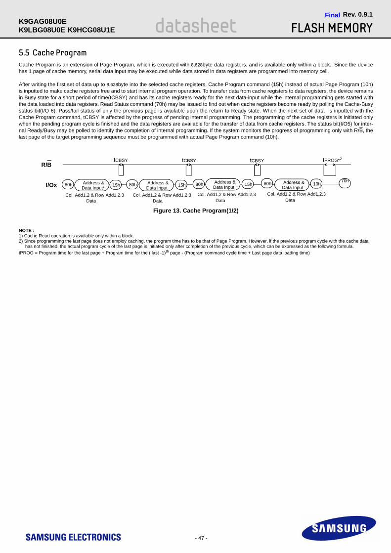
- 47 -
datasheet FLASH MEMORYRev. 0.9.1
K9LBG08U0E
FinalK9GAG08U0E
K9HCG08U1E
5.5 Cache ProgramCache Program is an extension of Page Program, which is executed with 8,628byte data registers, and is available only within a block. Since the device has 1 page of cache memory, serial data input may be executed while data stored in data registers are programmed into memory cell.
After writing the first set of data up to 8,628byte into the selected cache registers, Cache Program command (15h) instead of actual Page Program (10h) is inputted to make cache registers free and to start internal program operation. To transfer data from cache registers to data registers, the device remains in Busy state for a short period of time(tCBSY) and has its cache registers ready for the next data-input while the internal programming gets started with the data loaded into data registers. Read Status command (70h) may be issued to find out when cache registers become ready by polling the Cache-Busy status bit(I/O 6). Pass/fail status of only the previous page is available upon the return to Ready state. When the next set of data is inputted with the Cache Program command, tCBSY is affected by the progress of pending internal programming. The programming of the cache registers is initiated only when the pending program cycle is finished and the data registers are available for the transfer of data from cache registers. The status bit(I/O5) for inter-nal Ready/Busy may be polled to identify the completion of internal programming. If the system monitors the progress of programming only with R/B, the last page of the target programming sequence must be programmed with actual Page Program command (10h).
Figure 13. Cache Program(1/2)
80h
R/B
80h Address & Data Input 15h 80h Address &
Data Input 15h 80h Address & Data Input
10h
tCBSY tCBSY tCBSY tPROG*2
70h Address & Data Input* 15h
Col. Add1,2 & Row Add1,2,3 Col. Add1,2 & Row Add1,2,3 Col. Add1,2 & Row Add1,2,3Data Data Data
Col. Add1,2 & Row Add1,2,3Data
I/Ox
NOTE :1) Cache Read operation is available only within a block.2) Since programming the last page does not employ caching, the program time has to be that of Page Program. However, if the previous program cycle with the cache data has not finished, the actual program cycle of the last page is initiated only after completion of the previous cycle, which can be expressed as the following formula.tPROG = Program time for the last page + Program time for the ( last -1)th page - (Program command cycle time + Last page data loading time)

Figure 14. Cache Program(2/2)
- 48 -
datasheet FLASH MEMORYRev. 0.9.1
K9LBG08U0E
FinalK9GAG08U0E
K9HCG08U1E
15h
Page
K
Cac
he re
gist
er
data
regi
ster
CE
CLE
R/B
WE
ALE
RE
80h
Din N
Din
15h
M
Max
. 127
tim
es re
peat
able
≈
≈
≈
Last
Pag
e In
put &
Pro
gram
Din N
Din
10h
≈
≈
I/O80
h70
hM
I/Ox
≈
Page
KPa
ge K
Page
K+1
page
K
page
Kpa
ge K
+1
page
K+1
page
K
1
12
2
3
34
34
4
10h
NO
TE :
- Is
suin
g th
e 15
h co
mm
and
to th
e de
vice
afte
r ser
ial d
ata
inpu
t ini
tiate
s th
e pr
ogra
m o
pera
tion
with
cac
he re
gist
ers.
1. D
ata
for P
age
K is
inpu
t to
cach
e re
gist
ers.
2. D
ata
is tr
ansf
erre
d to
the
data
regi
ster
s by
the
15h
com
man
d. D
urin
g th
e tra
nsfe
r the
Rea
dy/B
usy
outp
uts
Bus
y St
ate
(tCB
SY
).3.
Dat
a fo
r Pag
e K
+1 is
inpu
t to
cach
e re
gist
ers
whi
le th
e da
ta o
f the
Pag
e K
is b
eing
pro
gram
med
.4.
The
pro
gram
min
g w
ith c
ache
regi
ster
s is
term
inat
ed b
y th
e 10
h co
mm
and
. Whe
n th
e de
vice
bec
omes
Rea
dy, i
t sho
ws
that
the
inte
rnal
pro
gram
min
g of
the
Pag
e K
+1 is
com
plet
ed.
tP
RO
G* =
Pro
gram
tim
e fo
r the
last
pag
e +
Prog
ram
tim
e fo
r the
( la
st -1
)th p
age
- (co
mm
and
inpu
t cyc
le ti
me
+ ad
dres
s in
put c
ycle
tim
e +
Last
pag
e da
ta lo
adin
g tim
e)
tCB
SY
tPR
OG
*

Pas
s/Fa
il st
atus
for e
ach
page
pro
gram
med
by
the
Cac
he P
rogr
am o
pera
tion
can
be d
etec
ted
by th
e R
ead
Stat
us o
pera
tion.
• I/
O 0
: P
ass/
Fail
of th
e cu
rren
t pag
e pr
ogra
m o
pera
tion.
• I/
O 1
: P
ass/
Fail
of th
e pr
evio
us p
age
prog
ram
ope
ratio
n.Th
e P
ass/
Fail
stat
us o
n I/O
0 a
nd I/
O 1
are
val
id u
nder
the
follo
win
g co
nditi
ons.
• S
tatu
s on
I/O
0 :
True
Rea
dy/B
usy
is R
eady
sta
te.
T
he T
rue
Rea
dy/B
usy
is o
utpu
t on
I/O 5
by
Rea
d St
atus
ope
ratio
n or
R/B
pin
afte
r the
10h
com
man
d. •
Sta
tus
on I/
O 1
:Cac
he R
ead/
Bus
y is
Rea
dy S
tate
.
The
Cac
he R
eady
/Bus
y is
out
put o
n I/O
6 b
y R
ead
Stat
us o
pera
tion
or R
/B p
in a
fter t
he 1
5h c
omm
and.
Exa
mpl
e)
70h
80h.
...15
hS
tatu
sO
ut80
h....
15h
70h
Sta
tus
Out
70h
Sta
tus
Out
80h.
...15
h
I/O1
=>
Inva
lid
Pa
ge1
P
age1
Pag
e N
-2
I
nval
id
P
age
N-1
70h
Sta
tus
Out
80h.
...10
h70
hS
tatu
sO
ut70
hSt
atus
Out
I/O0
=>
Inva
lid
In
valid
P
age2
Inva
lid
In
valid
Pag
e N
Pag
e 1
Pag
e 2
Pag
e N
-1Pa
ge N
R/B
pin
Cach
e
True
Pag
e 1
Pag
e 2
Page
N-1
Pag
e N
Rea
dy/B
usy
Rea
dy/B
usy
Dur
ing
both
Tru
e R
eady
/Bus
y an
d C
ache
Rea
dy/B
usy
retu
rn to
Rea
dy s
tate
, the
Pas
s/Fa
il fo
r pre
viou
spa
ge a
nd c
urre
nt p
age
can
be s
how
n th
roug
h I/O
1 a
nd I/
O 0
con
curr
ently
.
- 49 -
datasheet FLASH MEMORYRev. 0.9.1
K9LBG08U0E
FinalK9GAG08U0E
K9HCG08U1E
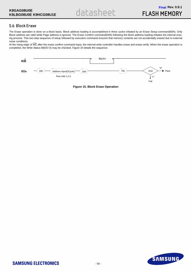
- 50 -
datasheet FLASH MEMORYRev. 0.9.1
K9LBG08U0E
FinalK9GAG08U0E
K9HCG08U1E
5.6 Block EraseThe Erase operation is done on a block basis. Block address loading is accomplished in three cycles initiated by an Erase Setup command(60h). Only Block address are valid while Page address is ignored. The Erase Confirm command(D0h) following the block address loading initiates the internal eras-ing process. This two-step sequence of setup followed by execution command ensures that memory contents are not accidentally erased due to external noise conditions.At the rising edge of WE after the erase confirm command input, the internal write controller handles erase and erase-verify. When the erase operation is completed, the Write Status Bit(I/O 0) may be checked. Figure 20 details the sequence.
Figure 15. Block Erase Operation
60h
Row Add 1,2,3
R/B
Address Input(3Cycle) I/O0 PassD0h 70h
tBERS
I/Ox"0"
"1"
Fail

- 51 -
datasheet FLASH MEMORYRev. 0.9.1
K9LBG08U0E
FinalK9GAG08U0E
K9HCG08U1E
5.7 Read StatusThe device contains a Status Register which may be read to find out whether program or erase operation is completed, and whether the program or erase operation is completed successfully. After writing 70h or F1h/F2h command to the command register, a read cycle outputs the content of the Status Reg-ister to the I/O pins on the falling edge of CE or RE, whichever occurs last. This two line control allows the system to poll the progress of each device in multiple memory connections even when R/B pins are common-wired. RE or CE does not need to be toggled for updated status. Refer to Table 2 for spe-cific 70h Status Register definitions and Table 3 for specific F1h status Register definitions. The command register remains in Status Read mode until fur-ther commands are issued to it. Therefore, if the status register is read during a random read cycle, the read command(00h) should be given before starting read cycles.
[Table 4] Status Register Definition for 70h Command
NOTE : 1) I/Os defined ’Not use’ are recommended to be masked out when Read Status is being executed.2) N : current page, N-1: previous page.
[Table 5] F1h Read Status Register Definition
NOTE :1) I/Os defined ’Not use’ are recommended to be masked out when Read Status is being executed.2) N : current page, N-1 : previous page.
[Table 6] F2h Read Status Register Definition
NOTE :1) I/Os defined ’Not use’ are recommended to be masked out when Read Status is being executed.2) N : current page, N-1 : previous page.
I/O Page Program Block Erase Cache Program Read Cache Read Definition
I/O 0 Pass/Fail Pass/Fail Pass/Fail(N) Not Use Not Use Pass : "0" Fail : "1"
I/O 1 Not Use Not Use Pass/Fail(N-1) Not Use Not Use Pass : "0" Fail : "1"
I/O 2 Not Use Not Use Not Use Not Use Not Use Don’t -cared
I/O 3 Not Use Not Use Not Use Not Use Not Use Don’t -cared
I/O 4 Not Use Not Use Not Use Not Use Not Use Don’t -cared
I/O 5 Not Use Not Use True Ready/Busy Not Use True Ready/Busy Busy : "0" Ready : "1"
I/O 6 Ready/Busy Ready/Busy Cache Ready/Busy Ready/Busy Cache Ready/Busy Busy : "0" Ready : "1"
I/O 7 Write Protect Write Protect Write Protect Write Protect Write Protect Protected : "0" Not Protected : "1"
I/O Page Program Block Erase Cache Program Read Cache Read Definition
I/O 0 Chip1 Pass/Fail Chip1 Pass/Fail Chip1 Pass/Fail(N) Not Use Not Use Pass : "0" Fail : "1"
I/O 1 Plane Pass/Fail Plane Pass/Fail Plane Pass/Fail(N) Not Use Not Use Pass : "0" Fail : "1"
I/O 2 Not Use Not Use Not Use Not Use Not Use Don‘t-cared
I/O 3 Not Use Not Use Plane Pass/Fail(N-1) Not Use Not Use Pass : "0" Fail : "1"
I/O 4 Not Use Not Use Not Use Not Use Not Use Don‘t-cared
I/O 5 Not Use Not Use True Ready/Busy Not Use True Ready/Busy Busy : "0" Ready : "1"
I/O 6 Ready/Busy Ready/Busy Cache Ready/Cache Ready/Busy Cache Ready/Busy Busy : "0" Ready : "1"
I/O 7 Write Protect Write Protect Write Protect Write Protect Write Protect Protected : "0" Not Protected : "1"
I/O Page Program Block Erase Cache Program Read Cache Read Definition
I/O 0 Chip2 Pass/Fail Chip2 Pass/Fail Chip2 Pass/Fail(N) Not Use Not Use Pass : "0" Fail : "1"
I/O 1 Plane Pass/Fail Plane Pass/Fail Plane Pass/Fail(N) Not Use Not Use Pass : "0" Fail : "1"
I/O 2 Not Use Not Use Not Use Not Use Not Use Don‘t-cared
I/O 3 Not Use Not Use Plane Pass/Fail(N-1) Not Use Not Use Pass : "0" Fail : "1"
I/O 4 Not Use Not Use Not Use Not Use Not Use Don‘t-cared
I/O 5 Not Use Not Use True Ready/Busy Not Use True Ready/Busy Busy : "0" Ready : "1"
I/O 6 Ready/Busy Ready/Busy Cache Ready/Cache Ready/Busy Cache Ready/Busy Busy : "0" Ready : "1"
I/O 7 Write Protect Write Protect Write Protect Write Protect Write Protect Protected : "0" Not Protected : "1"

- 52 -
datasheet FLASH MEMORYRev. 0.9.1
K9LBG08U0E
FinalK9GAG08U0E
K9HCG08U1E
5.8 Read IDThe device contains a product identification mode, initiated by writing 90h to the command register, followed by an address input of 00h. Six read cycles sequentially output the manufacturer code(ECh), the device code, 3rd, 4th, 5th and 6th cycle ID respectively. The command register remains in Read ID mode until further commands are issued to it. Figure 22 shows the operation sequence.
Figure 16. Read ID Operation
CE
CLE
I/OX
ALE
RE
WE
90h 00h
Address. 1cycle Maker code Device code
tCEA
tAR
tREA
tWHR
tCLR
Device4th Cyc.CodeECh 3rd Cyc. 5th Cyc. 6th Cyc.
5.9 RESETThe device offers a reset feature, executed by writing FFh to the command register. When the device is in Busy state during random read, program or erase mode, the reset operation will abort these operations. The contents of memory cells being altered are no longer valid, as the data will be partially programmed or erased. The command register is cleared to wait for the next command, and the Status Register is cleared to value E0h when WP is high. Refer toTable 7 for device status after reset operation. If the device is already in reset state a new reset command will be accepted by the command reg-ister. The R/B pin changes to low for tRST after the Reset command is written. Refer to Figure 17 below.
Figure 17. RESET Operation
FFhI/OX
R/BtRST
[Table 7] Device Status
Device Device Code (2nd Cycle) 3rd Cycle 4th Cycle 5th Cycle 6th Cycle
K9GAG08U0E D5h 84h72h
50h42hK9LBG08U0E D7h C5h 54h
K9HCG08U1E
After Reset
Operation Mode Waiting for next command

- 53 -
datasheet FLASH MEMORYRev. 0.9.1
K9LBG08U0E
FinalK9GAG08U0E
K9HCG08U1E
5.10 Ready/BusyThe device has a R/B output that provides a hardware method of indicating the completion of a page program, erase and random read completion. The R/B pin is normally high but transitions to low after program or erase command is written to the command register or random read is started after address loading. It returns to high when the internal controller has finished the operation. The pin is an open-drain driver thereby allowing two or more R/B outputs to be Or-tied. Because pull-up resistor value is related to tr(R/B) and current drain during busy(ibusy) , an appropriate value can be obtained with the fol-lowing reference chart(Figure 18). Its value can be determined by the following guidance.
Figure 18. Rp vs tr ,tf & Rp vs ibusy
tr,tf
[s]
Ibus
y [A
]
Rp(ohm)
Ibusy
tr
@ Vcc = 3.3V, Ta = 25°C , CL = 50pF
1K 2K 3K 4K
100n
200n 2m
1m
50
tf
100
150
200
3.6 3.6 3.6 3.6
2.4
1.2
0.8
0.6
where IL is the sum of the input currents of all devices tied to the R/B pin.
Rp value guidance
Rp(max) is determined by maximum permissible limit of tr
Rp(min, 3.3V part) =VCC(Max.) - VOL(Max.)
IOL + ΣIL =
3.2V
8mA + ΣIL
VCC
R/Bopen drain output
Device
GND
Rp ibusy
CL
Busy
Ready Vcc
VOH
tf tr
VOL
3.3V device - VOL : 0.4V, VOH : 2.4V

- 54 -
datasheet FLASH MEMORYRev. 0.9.1
K9LBG08U0E
FinalK9GAG08U0E
K9HCG08U1E
6.0 DATA PROTECTION & POWER UP SEQUENCEThe device is designed to offer protection from any involuntary program/erase during power-transitions. An internal voltage detector disables all functions whenever Vcc is below about 2V. The Reset command(FFh) must be issued to all CEs as the first command after the NAND Flash device is powered on. Each CE will be busy for a maximum of 5ms after a RESET command is issued. In this time period, the acceptable command is 70h/F1h/F2h.WP pin provices hardware protection and is recommanded to be kept at VIL during power-up and power-down. The two step command sequence for pro-gram/erase provides additional software protection.
Figure 19. AC Waveforms for Power Transition
VCC
WP
High
≈≈
WE≈
≈
R/B100μs
~ 2.7V ~ 2.7V
Invalid Don’t care
Don’t care
CLE
≈≈
CE
≈≈
I/Ox FFh
≈≈
5ms max
Don’t care
≈
Operation
100μs
NOTE :During the initialization, the device consumes a maximum current of 50mA (ICC1)

- 55 -
datasheet FLASH MEMORYRev. 0.9.1
K9LBG08U0E
FinalK9GAG08U0E
K9HCG08U1E
6.1 WP AC Timing guideEnabling WP during erase and program busy is prohibited. The erase and program operations are enabled and disabled as follows:
Figure B-1. Program Operation
Figure B-2. Erase Operation
1. Enable Mode
≈
60h D0h
tww(min.100ns)
2. Disable Mode
≈
60h D0h
tww(min.100ns)
WE
I/O
WP
R/B
WE
I/O
WP
R/B
1. Enable Mode
≈
80h 10h
WE
I/O
WP
R/B tww(min.100ns)
2. Disable Mode
≈
80h 10h
tww(min.100ns)
WE
I/O
WP
R/B