final
TRANSCRIPT


Welcome to theMicroCotrollers,MicroProcessors,
DSP,Tools & RTOS seminar Amir Sherman –
FAE Manager ,Arrow Israel

Agenda
• Microcontrollers Market Changes
•What is ARM and how they change the world
•Every Supplier need to fit to the market so Arrow Bring it to you .
•What will come in the Future

•Advanced Microcontroller Bus Architecture1
•AHB and APB / VPB
High-bandwidth on-
chip RAM
ARM core
DMA Bus Master
High-bandwidth
Memory Interface
UART
Timer
Keypad
Display
APBAPB Bridge
RTC
I/O
AHB
•Advanced High-Performance Bus •Advanced Peripheral Bus /
VLSI Peripheral Bus


ARM966E Benefits vs. ARM7TDMI
F = FetchD = DecodeE = ExecuteM = Memory ReadW = Memory Write-Back
F D E M WF D E M W
F D E M WF D E M W
F D E M W
F D E MF D E
F DF
5-STAGE PIPELINE
CPUCORE
F D E F DF D E F D
F D E F D
E F D EE F D
E F
3-STAGE PIPELINE
CPUCORE
ARM966E
ARM7TDMI
AHB/APB
BUS/APB
F D E M WF D E M W
F D E M WF D E M W
F D E M W
F D E MF D E
F DF
CODE5-STAGE PIPELINE
F D E F DF D E F D
F D E F D
E F D EE F D
E F
3-STAGE PIPELINE
DMI
Harvard Architecture
Von Neumann Architecture
CODE & DATA
DATA
CPUCORE
CODEMEMORY
DATAMEMORY
CPUCORE
CODE ANDDATA
MEMORYCOMBINED
ARM966E
ARM7T
AHB/APB
BUS/APB


New Architecture in ARM7 TDMI-S


Development ToolsAvailable from traditional 8-bit
tool providers as well as established 32-bit providers


JTAG Emulators

Debuggers/Simulators (1)
Pathfinder debugger
ARM RealView debugger
MULTI Debugger
C-SPY debugger ARM

Debuggers/Simulators (2)
Keil debugger &
simulator µVision3
Seehau debugger ARM
Universal Debug
Engine (UDE)
Chameleon Debugger

Compilers
ARM Compiler
GNU GCC
GHS Compiler
IAR Compiler

IDE’s - Integrated Development Environment

RTOS & Stacks

Arrow’s Solutionsto you !


EDN LPC210x award2006

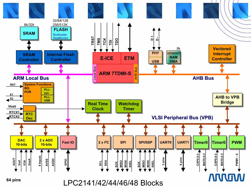
ETMETM
Vectored Interrupt
Controller
Vectored Interrupt
Controller
AHB BusAHB BusARM Local BusARM Local Bus
VLSI Peripheral Bus (VPB)VLSI Peripheral Bus (VPB)
AHB to VPB Bridge
AHB to VPB Bridge
WatchdogTimer
WatchdogTimer
RTC Osc
Vbatt
RTCX1RTCX2
Real TimeClock
Real TimeClock
UART0UART0
2 pi
ns
UART1UART1
8 pi
ns
2 x I2C2 x I2C
SCL
SDA
ADC10-bitsADC
10-bits
8 In
puts
AVS
S
AVD
D
SRAMController
SRAMController
SRAMSRAM
Internal FlashController
Internal FlashController
FLASHFLASHBootloader,RealMonitor
SPISPI
SCK
MIS
OM
OSI
SSEL
SPI/SSPSPI/SSP
SCK
MIS
OM
OSI
SSEL
Timer032-bit
Timer032-bit
3 x
CA
P0
3 x
MA
T0
Timer132-bit
Timer132-bit
4 x
CA
P1
4 x
MA
T1
8/16/32Kb2/4/8Kb
TCK
TMS
TDI
TDO
TRST
E-ICE
ARM 7TDMI-SARM 7TDMI-S
AH
B B
us
Loca
l Bus
FastGPIOFastGPIO
GPI
O
SystemFunctions
SystemFunctions
PLLPLL
RST
X1X2
Timer216-bit
Timer216-bit
3 x
CA
P2
3 x
MA
T2
Timer316-bit
Timer316-bit
4 x
MA
T3
70MHz
1$(50Kpcs)
LPC2101/2/3 Blocks48 pins

EDN LPC213x &LPC214x award
2006

Vectored Interrupt
Controller
Vectored Interrupt
Controller
TCK
TMS
TDI
TDO
TRST
E-ICE ETMETM
ARM 7TDMI-SARM 7TDMI-SAHB BusAHB BusA
HB
Bus
Loca
l Bus
VLSI Peripheral Bus (VPBVLSI Peripheral Bus (VPB))
AHB to VPB Bridge
AHB to VPB Bridge
Fast IO(1)
Fast IO(1)
GPI
O
WatchdogTimer
WatchdogTimer
RTC Osc
Supply
RTCX1RTCX2
Real TimeClock
Real TimeClock
UART0UART0
2 pi
ns
UART1UART1
8 pi
ns
2 x I2C2 x I2C
SCL
SDA
2 x ADC10-bits
2 x ADC10-bits
8 In
puts
AVS
S
AVD
D
DAC10-bitsDAC
10-bits
AO
UT
V3A
Vref
VssA
SRAMController
SRAMController
SRAMSRAM
Internal FlashController
Internal FlashController
FLASHFLASHBootloader,RealMonitor
SystemFunctionsBO, POR
SystemFunctionsBO, POR
PLLPLL
RST
X1X2
SPISPI
SCK
MIS
OM
OSI
SSEL
SPI/SSPSPI/SSPSC
KM
ISO
MO
SISS
EL
Timer0Timer0
CA
P0.0
-3
MA
T0.0
-3
PWMPWM
PWM
1 -6
Timer0Timer0
CA
P0.0
-3
MA
T0.0
-3
32/64/12816/32k
ARM Local BusARM Local Bus
256/512K
(1) /01 version only
LPC2131/32/34/36/38 Blocks version /0164 pins
Vectored Interrupt
Controller
Vectored Interrupt
Controller
TCK
TMS
TDI
TDO
TRST
E-ICE ETMETM
ARM 7TDMI-SARM 7TDMI-SAHB BusAHB BusA
HB
Bus
ARM Local BusARM Local Bus Loca
l Bus
VLSI Peripheral Bus (VPB)VLSI Peripheral Bus (VPB)
AHB to VPB Bridge
AHB to VPB Bridge
Fast IOFast IO
GPI
O
WatchdogTimer
WatchdogTimer
RTC Osc
Vbatt
RTCX1RTCX2
Real TimeClock
Real TimeClock
UART0UART0
2 pi
ns
UART1UART1
8 pi
ns
2 x I2C2 x I2C
SCL
SDA
2 x ADC10-bits
2 x ADC10-bits
8 In
puts
AVS
S
AVD
D
DAC10-bitsDAC
10-bits
AO
UT
V3A
Vref
VssA
SRAMController
SRAMController
SRAMSRAM
Internal FlashController
Internal FlashController
FLASHFLASHBootloader,RealMonitor
SPISPI
SCK
MIS
OM
OSI
SSEL
SPI/SSPSPI/SSPSC
KM
ISO
MO
SISS
EL
Timer0Timer0
CA
P0.0
-3
MA
T0.0
-3
PWMPWM
PWM
1 -6
Timer0Timer0
CA
P0.0
-3
MA
T0.0
-3
System FunctionsBO,POR
System FunctionsBO,POR
PLL-USB
PLL-USB
RST
X1X2
PLL-sys
PHY
USB
PHY
USB
D +
D -
(shared)RAMDMA
(shared)RAMDMA
8k/32k
8k
32/64/128256/512K
64 pins LPC2141/42/44/46/48 Blocks

Arrow Israel
award for LPC2880/8
in 2007

Txd,
Rxd
RTS
, CTS
Internal FlashController
Internal FlashController
FLASHFLASH
VLSI Peripheral Bus (VPBVLSI Peripheral Bus (VPB))
Vectored Interrupt
Controller
Vectored Interrupt
Controller
AHB to APB Bridges 0, 1, 2, 3
AHB to APB Bridges 0, 1, 2, 3
WatchdogTimer
WatchdogTimer
Real TimeClock
Real TimeClock
AHB BusAHB BusARM Local BusARM Local Bus
TCK
TMS
TDI
TDO
TRST
E-ICE
ARM 7TDMI-SARM 7TDMI-S
AH
B B
us
Loca
l Bus
External Static MemoryController
(SDRAM/Flash/SRAM)SRAM
ControllerSRAM
Controller
SRAMSRAM64k 1MB (1)
SPISPI
SCK
MIS
O
MO
SISS
ELUARTWithIrDA
UARTWithIrDA
SD/MMCcard
SD/MMCcard
MD
[3:0
]
Timer0Timer0
CA
P0.0
-3
MA
T0.0
-3
Timer1Timer1
CA
P1.0
-3
MA
T1.0
-3
PWMPWM
PWM
1 -6
LCDLCD
LCD
Bus
GPIO85x
GPIO85x
GPI
O
I2CI2C
SCL
SDA
ADC10-bitsADC
10-bits
4 In
puts
2x
System FunctionsBO,POR
System FunctionsBO,POR
PLL-USB
PLL-USB
RST
X1X2
PLL-sys
8KB Cache8KB Cache HS USBWithDMA
HS USBWithDMA
RTC Osc
RTCX1RTCX2
MC
LK
I²SIn/Out
I²SIn/Out
DA
TI
DA
TO, B
CK
O,
DC
LKO
,WSO
BC
KI,
WSI
GP DMAControllerGP DMA
Controller
SEL
ROMController
ROMController
BootROMBootROM
(1) LPC2888 only
180 pins LPC2880/88 Blocks

35
With a single bus, the CPU, Ethernet and USB all contend for bandwidth, potentially causing a
communications “traffic jam”
The solution is the NXP LPC2300/2400

Arrow Israel
award for LPC23xx
in 2007

WatchdogTimer
WatchdogTimer
SRAMController
SRAMController
SRAMSRAM
Internal FlashController
Internal FlashController
FLASHFLASHBootloader,RealMonitorBootloader,RealMonitor
Real TimeClock
Real TimeClockRTC
Osc
Vbatt
RTCX1RTCX2
RAM2KB
RAM2KB
Vectored Interrupt
Controller
Vectored Interrupt
Controller
SRAM16KB
SRAM16KB
Ethernet MAC, RMII, 10/100,
DMA
Ethernet MAC, RMII, 10/100,
DMA
SystemFunctions,POR, BO
SystemFunctions,POR, BO
RST
X1X2
PLL
Osc. IRC4MHzOsc.
AHB1 to APB Bridge
AHB1 to APB Bridge
APB
ADC10-bitsADC
10-bits
Result reg.’s
Inpu
ts
AVS
S
AVD
D
GPIOGPIOFast I/O
GPI
O
Timer0,1,2,3
32 bit
Timer0,1,2,3
32 bit
CA
P0.0
-3
MA
T0.0
-3
EICE ETMETM
ARM 7TDMI-SARM 7TDMI-S
AHB1
AHB2
AH
B B
ridge
ARM Local Bus Loca
l Bus
JTAGDebug
Trace
PWM1
32 bit
PWM1
32 bit
PWM
1 -6
PCA
P0-1
126/256/512K8/32/32K
I2SI2S
6 pi
ns
3I2CI2C
3
SCL
SDA
2CANCAN
2
TX 0
,1
RX
0,1
UART1UART1Fr.B.r. gen.
8 pi
ns
SSPSSP
SCK
MIS
O
MO
SISS
EL
UART0,2,3
UART0,2,3
Fr.B.r. gen.
3
2 pi
ns
SSP,SPI
SSP,SPI
SCK
MIS
O
MO
SISS
EL
2SD/MMC
Card SD/MMC
Card
MC
ICLK
, M
CIP
WR
MC
ICM
D,
MC
IDA
T3:0
70
GP DMAControllerGP DMA
ControllerRAM8KB
RAM8KB
USB,DMA
USB,DMA PH
YRAM4KB
MasterMaster
AHB to AHB Bridge
AHB to AHB Bridge
SlaveSlave
DAC10-bitsDAC
10-bits
AO
UT
V3A
Vref
VssA
LPC2364/66/68 Blocks100 pins

WatchdogTimer
WatchdogTimer
SRAMController
SRAMController
SRAMSRAM
Internal FlashController
Internal FlashController
FLASHFLASHBootloader,RealMonitorBootloader,RealMonitor
Real TimeClock
Real TimeClockRTC
Osc
Vbatt
RTCX1RTCX2
RAM2KB
RAM2KB
Vectored Interrupt
Controller
Vectored Interrupt
Controller
SRAM16KB
SRAM16KB
External Memory
Controller
External Memory
Controller
Ethernet MAC, RMII, 10/100,
DMA
Ethernet MAC, RMII, 10/100,
DMA
SystemFunctions,POR, BO
SystemFunctions,POR, BO
RST
X1X2
PLL
Osc. IRC4MHzOsc.
AHB1 to APB Bridge
AHB1 to APB Bridge
APB
ADC10-bitsADC
10-bits
Result reg.’s
Inpu
ts
AVS
S
AVD
D
GPIOGPIOFast I/O
GPI
O
Timer0,1,2,3
32 bit
Timer0,1,2,3
32 bit
CA
P0.0
-3
MA
T0.0
-3
EICE ETMETM
ARM 7TDMI-SARM 7TDMI-S
AHB1
AHB2
AH
B B
ridge
ARM Local Bus Loca
l Bus
JTAGDebug
Trace
PWM1
32 bit
PWM1
32 bit
PWM
1 -6
PCA
P0-1
512K32K
I2SI2S
6 pi
ns
3I2CI2C
3
SCL
SDA
2CANCAN
2
TX 0
,1
RX
0,1
UART1UART1Fr.B.r. gen.
8 pi
ns
SSPSSP
SCK
MIS
O
MO
SISS
EL
UART0,2,3
UART0,2,3
Fr.B.r. gen.
3
2 pi
ns
SSP,SPI
SSP,SPI
SCK
MIS
O
MO
SISS
EL
2SD/MMC
Card SD/MMC
Card
MC
ICLK
, M
CIP
WR
MC
ICM
D,
MC
IDA
T3:0
Alarm
104
GP DMAControllerGP DMA
ControllerRAM8KB
RAM8KB
USB,DMA
USB,DMA PH
YRAM4KB
MasterMaster
AHB to AHB Bridge
AHB to AHB Bridge
SlaveSlave
DAC10-bitsDAC
10-bits
AO
UT
V3A
Vref
VssA
8/64
144 pins LPC2378 Block

Arrow Israel
award for LPC24xx
in 2007

MasterMaster
AHB to AHB Bridge
AHB to AHB Bridge
SlaveSlave
WatchdogTimer
WatchdogTimer
SRAMController
SRAMController
SRAMSRAM
Internal FlashController
Internal FlashController
FLASHFLASHBootloader,RealMonitorBootloader,RealMonitor
Real TimeClock
Real TimeClockRTC
Osc
Vbatt
RTCX1RTCX2
RAM2KB
RAM2KB
Vectored Interrupt
Controller
Vectored Interrupt
Controller
SRAM16KB
SRAM16KB
External Memory
Controller
External Memory
Controller
Ethernet MAC, MII/RMII, 10/100,
DMA
Ethernet MAC, MII/RMII, 10/100,
DMA
SystemFunctions,POR, BO
SystemFunctions,POR, BO
RST
X1X2
PLL
Osc. IRC4MHzOsc.
AHB1 to APB Bridge
AHB1 to APB Bridge
APB
ADC10-bitsADC
10-bits
Result reg.’s
Inpu
ts
AVS
S
AVD
D
GPIOGPIOFast I/O
GPI
O
Timer0,1,2,3
32 bit
Timer0,1,2,3
32 bit
CA
P0.0
-3
MA
T0.0
-3
EICE ETMETM
ARM 7TDMI-SARM 7TDMI-S
AHB1
AHB2
AH
B B
ridge
ARM Local Bus Loca
l Bus
JTAGDebug
Trace
PWM0,1
32 bit
PWM0,1
32 bit
PWM
1 -6
PCA
P0-1
512K64K
I2SI2S
6 pi
ns
3I2CI2C
3
SCL
SDA
2CANCAN
2
TX 0
,1
RX
0,1
UART1UART1Fr.B.r. gen.
8 pi
ns
SSPSSP
SCK
MIS
O
MO
SISS
EL
UART0,2,3
UART0,2,3
Fr.B.r. gen.
3
2 pi
ns
SSP,SPI
SSP,SPI
SCK
MIS
O
MO
SISS
EL
2SD/MMC
Card SD/MMC
Card
MC
ICLK
, M
CIP
WR
MC
ICM
D,
MC
IDA
T3:0
Alarm
160
GP DMAControllerGP DMA
ControllerRAM16KB
RAM16KB
USB,otg,DMA
USB,otg,DMA PH
YRAM4KB
DAC10-bitsDAC
10-bits
AO
UT
V3A
Vref
VssA
LPC2468 Block208 pins

Real TimeClock
Real TimeClockRTC
Osc
Vbatt
RTCX1RTCX2
RAM2KB
RAM2KB
SystemFunctions,POR, BO
SystemFunctions,POR, BO
RST
X1X2
PLL
Osc. IRC4MHzOsc.
AHB1 to APB Bridge
AHB1 to APB Bridge
APBAlarm
MasterMaster
AHB to AHB Bridge
AHB to AHB Bridge
SlaveSlave
WatchdogTimer
WatchdogTimer
SRAMController
SRAMController
SRAMSRAM
Internal FlashController
Internal FlashController
FLASHFLASHBootloader,RealMonitorBootloader,RealMonitor
Vectored Interrupt
Controller
Vectored Interrupt
Controller
SRAM16KB
SRAM16KB
External Memory
Controller
External Memory
Controller
Ethernet MAC, MII/RMII, 10/100,
DMA
Ethernet MAC, MII/RMII, 10/100,
DMA
ADC10-bitsADC
10-bits
Result reg.’s
Inpu
ts
AVS
S
AVD
D
GPIOGPIOFast I/O
GPI
O
Timer0,1,2,3
32 bit
Timer0,1,2,3
32 bit
CA
P0.0
-3
MA
T0.0
-3
EICE ETMETM
ARM 7TDMI-SARM 7TDMI-S
AHB1
AHB2
AH
B B
ridge
Loca
l Bus
JTAGDebug
Trace
PWM0,1
32 bit
PWM0,1
32 bit
PWM
1 -6
PCA
P0-1
0/512K64K
I2SI2S
6 pi
ns
3I2CI2C
3
SCL
SDA
2CANCAN
2
TX 0
,1
RX
0,1
UART1UART1Fr.B.r. gen.
8 pi
ns
SSPSSP
SCK
MIS
O
MO
SISS
EL
UART0,2,3
UART0,2,3
Fr.B.r. gen.
3
2 pi
ns
SSP,SPI
SSP,SPI
SCK
MIS
O
MO
SISS
EL
2SD/MMC
Card SD/MMC
Card
MC
ICLK
, M
CIP
WR
MC
ICM
D,
MC
IDA
T3:0
160
GP DMAControllerGP DMA
ControllerRAM16KB
RAM16KB
USB,otg,DMA
USB,otg,DMA PH
YRAM4KB
DAC10-bitsDAC
10-bits
AO
UT
V3A
Vref
VssA
32/24
QVGAController
QVGAController
ARM Local Bus
LPC2470/78 Block208 pins


Arrow Israel
award for STR71x
in 2006

STR71xF Series Block Diagram
Deterministic Operation from Flash Memory
Large size SRAM and Flash Mem
USB and CAN Connectivity
External Memory Interface
12-bit Accuracy for ADC
AC
CEL
AC
CEL 64KB + 16KB,
128KB + 16KB, 256KB + 16KB Flash Memory
64KB + 16KB, 128KB + 16KB, 256KB + 16KB Flash Memory
16KB, 32KB, or 64KB SRAM16KB, 32KB, or 64KB SRAM
AR
M7
Nat
ive
Bus
AR
M7
Nat
ive
Bus
JTAG DebugJTAG Debug
ARM7TDMI CPU
50 MHz
ARM7TDMI CPU
50 MHz
Nested Interrupt Cntl
Nested Interrupt Cntl
AR
M P
erip
hera
l Bus
, APB
2A
RM
Per
iphe
ral B
us, A
PB 2
External MemInterface
External MemInterface
4 x 12-bit ADC4 x 12-bit ADC
AR
M P
erip
hera
l Bus
, A
PB1
AR
M P
erip
hera
l Bus
, A
PB1
1 x I2C1 x I2C
4 x 16-bit Timer4 x 16-bit Timer
Clock ControlClock Control
1 x I2C or 1 x SPI
1 x I2C or 1 x SPI
1 x SPI1 x SPI
1 x UART with SmartCard
1 x UART with SmartCard
3 x UART3 x UART
1 x CAN 2.0B1 x CAN 2.0B
1 x USB FS Device
1 x USB FS Device
1 x HDLC1 x HDLC
Up to 14 External Intr
Up to 14 External Intr
48 I/Os48 I/Os
WatchdogWatchdogRTC / WUURTC / WUU
32KHz Oscfrom Ext XTAL
32KHz Oscfrom Ext XTAL
PLLPLL
V Reg 1.8VV Reg 1.8V
BridgeBridge

STR73xF Series Block Diagram
Absolute Deterministic Operation from Flash Memory
True 5V Operation
Up to 20 Timers
Many CAN, UART, ADC, and SPI
Internal RC OscClock Generation
AH
BA
HB
64KB, 128KB, or 256KB
Flash Memory
64KB, 128KB, or 256KB
Flash Memory
16KB SRAM16KB SRAM
AR
M7
Nat
ive
Bus
AR
M7
Nat
ive
Bus
JTAG DebugJTAG Debug
ARM7TDMI CPU
36 MHz
ARM7TDMI CPU
36 MHz
Nested Interrupt Cntl
Nested Interrupt Cntl
AR
M P
erip
hera
l Bus
, APB
1A
RM
Per
iphe
ral B
us, A
PB1
12 or 16 x 10-bit ADC12 or 16 x 10-bit ADC
AR
M P
erip
hera
l Bus
, APB
0A
RM
Per
iphe
ral B
us, A
PB0 2 x I2C2 x I2C
3 x SPI3 x SPI
4 x UART4 x UART
3 x CAN 2.0B3 x CAN 2.0B
72 or 112 I/Os72 or 112 I/Os
WatchdogWatchdog
RTCRTC
PLL, Internal RC Osc
PLL, Internal RC Osc
Power Supply V Reg 1.8V
Power Supply V Reg 1.8V
Wake Up UnitWake Up Unit
3 x Time Base3 x Time Base
6 or 10 x 16-bit Timer
6 or 10 x 16-bit Timer
6 x 16-bit PWM6 x 16-bit PWM
Clock Management
Clock Management
APB
1A
PB1
4 Channel DMA
4 Channel DMA
Clock ControlClock Control
BridgeBridge

Arrow Israel
award for STR75x
in 2007

16KB SRAM16KB SRAM
AR
M L
iteH
i-Spe
ed B
usA
RM
Lite
Hi-S
peed
Bus
JTAG DebugJTAG Debug
ARM7TDMI CPU
60 MHz
ARM7TDMI CPU
60 MHz
Nested Intr CntlNested Intr Cntl
AR
M P
erip
hera
l Bus
AR
M P
erip
hera
l Bus
11 or 16 x 10-bit ADC11 or 16 x 10-bit ADC
AR
M P
erip
hera
l Bus
AR
M P
erip
hera
l Bus
1 x I2C1 x I2C
2 x SPI2 x SPI
3 x UART/LIN3 x UART/LIN
1 x CAN 2.0B1 x CAN 2.0B
32 or 72 I/Os32 or 72 I/OsWatchdogWatchdogRTCRTC
Oscs for 32KHz & 4MHz XTAL
Oscs for 32KHz & 4MHz XTAL
Internal RC OscInternal RC Osc
Power Supply V Reg 1.8V
Power Supply V Reg 1.8V
16 External Interrupts
16 External Interrupts
6 x 16-bit PWM Synchronized
6 x 16-bit PWM Synchronized
3 x 16-bit Timer 1 x Sys Timer
3 x 16-bit Timer 1 x Sys Timer
Clock ControlClock Control
1 x USB FS DEVICE
1 x USB FS DEVICE
PLLPLL
4 Channel DMA
4 Channel DMA
Mat
rix /
Arb
iter
Mat
rix /
Arb
iter
BridgeBridge
Wake Up Unit Wake Up Unit
SPI BootSPI Boot
AC
CEL
AC
CEL 64KB + 16KB,
128KB + 16KB, 256KB + 16KB Flash Memory
64KB + 16KB, 128KB + 16KB, 256KB + 16KB Flash Memory
54 peak MIPS operating directly from Flash memory
Excellent fail-safe clock modes
State-of-the-art motor control PWM controller
3V or 5V Supply
Low-power modes with internal wake-up
STR75xF Series Block Diagram

Arrow Israel
award for STR91x
in 2007

ITC
MIT
CM
AC
CEL
AC
CEL
256KB + 32KB, 512KB + 32KB
Burst Flash
256KB + 32KB, 512KB + 32KB
Burst Flash
64KB or 96KB SRAM
64KB or 96KB SRAMD
TCM
DTC
M
AR
BIT
ERA
RB
ITER
AR
M H
i-Spe
ed B
usA
RM
Hi-S
peed
Bus
JTAG & ETMJTAG & ETM
ARM966 CPU96MHz
withDSP Inst
ARM966 CPU96MHz
withDSP Inst
1 x Ethernet MAC w/DMA1 x Ethernet MAC w/DMA Intr Control
33 Priority LvlsIntr Control
33 Priority Lvls
AR
M P
erip
hB
usA
RM
Per
iph
Bus
BridgeBridge
1 x USB FS Device w/DMA1 x USB FS
Device w/DMA
1 x CAN 2.0B1 x CAN 2.0B
3-Phase Motor Control
3-Phase Motor Control
8 Channel DMA
8 Channel DMA
EMI, Data x8 or x16
EMI, Data x8 or x16
8 x 10-bit ADC8 x 10-bit ADC
POR LVD BOD
POR LVD BOD
Voltage Inputs:3.0V I/O, 1.8V
Core, Opt. Battery for RTC
and SRAM
Voltage Inputs:3.0V I/O, 1.8V
Core, Opt. Battery for RTC
and SRAM
AR
M P
erip
hera
l Bus
AR
M P
erip
hera
l Bus
2 x I2C2 x I2C
2 x SPI2 x SPI
3 x UART / IrDA
3 x UART / IrDA
Up to 80 I/OsUp to 80 I/Os
4 x 16-bit Timer
4 x 16-bit Timer
WatchdogWatchdog
RTC / WUURTC / WUU
Clock Control / Power Down
Clock Control / Power Down
PLLPLL
Crystal Inputs: Main &
Optional RTC
Crystal Inputs: Main &
Optional RTC
96 MIPS peak operating directly from Flash Memory
Ethernetconnectivity
Largest SRAM in Class
Highly Efficient Data Flow
Extensive Supervisor Functions
Excellent Low-Power Operation
ITCM = Instruction Tightly Coupled Memory ETM = Embedded Trace Module POR = Power-On Reset BOD = Brown Out DetectDTCM = Data Tightly Coupled Memory EMI = External Memory Interface LVD = Low Voltage Detect WUU = Wake Up Unit
STR91xF Series Block Diagram

LQFP80 LQFP128LQFP128
BGA
BGA
BGA
LQFP128
LQFP128
STR911FAW44544 KB F / 96 KB SUSB, CAN, EMI
STR911FAW42288 KB F / 96 KB SUSB, CAN, EMI
STR912FAW34544 KB F / 64 KB SENET, USB, CAN, EMI
BGA144 Option Avail
Coming Q207
Flash Density (bytes)
288K
544KSTR912FW44*544 KB F / 96 KB SENET, USB, CAN, EMI
STR912FW42*288 KB F / 96 KB SENET, USB, CAN, EMI
STR911FM44*544 KB F / 96 KB SUSB, CAN
STR911FM42*288 KB F / 96 KB SUSB, CAN
STR910FW32*288 KB F / 64 KB SCAN, EMI
STR910FM32*288 KB F / 64 KB SCAN
LQFP80 LQFP128 LQFP80 LQFP128
544K
Common Features to All Devices
• 96 peak MIPS at 96 MHz• I2C, SPI, UART, IrDA, 10b
ADC, RTC, TIMERS• Embedded Trace Module
(ETM9)
Production Now
1.1M
2.1M
LQFP80 LQFP128
BGA
BGA
STR912FAW472.1 MB F / 96 KB SENET, USB, CAN, EMI
BGA = STR912FAZ47
STR912FAW461.1 MB F / 96 KB SENET, USB, CAN, EMI
BGA = STR912FAZ46
STR911FAM461.1 MB F / 96KB SUSB, CAN
LQFP80
STR911FAM472.1 MB F / 96KB SUSB, CAN
LQFP128
STR911FAW472.1 MB F / 96KB SUSB, CAN, EMI
STR911FAW461.1 MB F / 96 KB SUSB, CAN, EMI
LQFP128
Development for Q307
BGA = STR910FAZ32 BGA = STR912FAZ42
BGA = STR912FAZ44
Capability* “FA” versions available Q207
STR91x Series, Now and Next

In the Low Power Market


Arrow Israel
award for i.MX21
in 2006

Freescalei.MX21 Portable Media Center
Reference Platform

i.MX21 Portable Media Center (PMC) PlatformExample Implementation Includes:•Freescale i.MX21 Apps Processor•64MB Flash, 64 MB SDRAM•3.6” 320x240 16-bit color LCD•Stereo headphone output•HS USB, Ethernet and UART support•4 Hours of video playback•Push-button based UI•WinCE PMC Bard support package•Demo hardware available for demonstration upon request

Block Diagram
i.
Comprehensive Media Player Reference Design KitSchematic: PDF and OrCADLayout: Gerber files of PCBBoard Support Packages:
Metrowerks “Buggles” Linux BSP from FreescalePMC WinCE5.0 from Microsoft, drivers from Freescale
Bill of Material: Complete parts list, Costed at volume Performance Data: Battery life, WMV frame rate and bit rate performance
Cost : Free of Charge
Available from the page:http://www.freescale.com/imx21or
http://www.freescale.com/webapp/sps/site/overview.jsp?nodeId=018rH3297349759983

Arrow Israel
award for i.MX27
& i.MX31
in 2007

CPU ComplexARM926EJ-S™ 400 MHz @1.6V, 266 MHz @1.2V*16 Kb L1 I- and D-caches16 Channel DMAArchitecture compatible with i.MX21ETM Real-Time Debug
Low PowerActive Well-BiasDynamic Process Temperature CompensationDynamic Voltage and Frequency Scaling
SecuritySahara2 Crypto Accelerator (AES, 3DES)Electronically-Blown Fuse Box for custom HW IDs
ConnectivityEthernet MAC6x UARTs, IrDA480 Mbps USBOTG + 2 Hosts
ExpansionMemStick Pro, PCMCIA/CF, MMC & SD/SDIO Card InterfaceATA-6 HDD Interface
MultimediaMPEG 4/ H.263/H.264 D1 @30fps HW Codecw/ pre- & post- processingHigh speed CMOS sensor I/F + I2C
External Memory Interface16/32-bit SDRAM @133 MHz16/32-bit DDR @266 MHz8/16-bit NAND Flash, PSRAM support
TechnologyLow power 90nm
Inherited from i.MX21Inherited from i.MX21 New or enhanced from i.MX21New or enhanced from i.MX21
i.MX27i.MX27 System ControlSystem Control
Clock Mgt.
Bootstrap
JTAG/ICEM
6 x Timer
GPIO
RTC
PWM
WD Timer
8x8 Keypad
Human InterfaceHuman InterfaceLCD ControlSmart LCD
Camera I/FMultimedia I/FMultimedia I/F
MPEG4/H.263
MultimediaAcceleratorMultimediaAccelerator
Pre & PostProcessing
MemoryInterfaceMemoryInterface
DDR/SDRAM
NAND Flash
EIM
ExpansionExpansion
MemStick Pro
PCMCIA / CF
ConnectivityConnectivity
1-Wire
IrDA
I2C x 2
InternalInternal
6 x UARTHS USB OTG
Hostx2
10/100 Ether.
i-cache d-cache MMU
Bus Control
Internal Control
MemoryControl
CPU ComplexCPU Complex
ARM926EJ-S™ Smart SpeedSwitch (MAX)
Audio MuxStd System I/OStd System I/O
DMA
ATA
H.264
2x I2S/SSI
3x CSPI
3x MMC/SD
Vsync Flash
SCCSecurity ControlSecurity Control
SAHARA2
IIM RTICRNGA
ExternalExternal
i.MX27 Multimedia Application Processor


In the Low Power Market

MC9RS08KA FamilyA New Leader at the Ultra-low End
MC9RS08KA2MC9RS08KA1
April 2006

MC9RS08KA• Supply Voltage / Performance• 1.8-5.5V
• Core• RS08 Core
• Memory• 1K / 2K Flash• 63 B RAM
• Analog Comparator• Full rail-to-rail supply operation• Can operate in STOP mode
• Features/ Benefits• Integrated Clock Source (ICS) up to 10MHz internal bus operation with 2% deviation over full temperature and voltage range
• Computer operating properly feature (COP)• 8-bit Modulo Timer• 3 / 5 channel keyboard interrupt (KBI)• LVD (low voltage detect) with reset or stop wakeup• External Vpp required for Flash programming• Auto wakeup• Background debug controller(BDC)
6 pin DFN, 8 pin NB-SOIC, 8 pin PDIP
1K/2K Flash
63 BRAM
LVD
BDC
ICS
KBI
Analog
Comp
8-bit
Modulo
Timer
COPRS08
Core

Key Features/Benefits• 4k Flash and 256B of RAM
• Supply Voltage/ Performance2.7V – 5.5V operation , -40 to +105C range4MHz bus @ 3.0 V ±10%, 8MHz bus @ 5.0 V ±10% operation
• Low pin count MCU8 pin package PDIP and NB SOIC
• Analog to Digital Converter (ADC)• 4 channel, 10 bit ADC with internal reference voltage
• Internal Clock Source (ICS)• ±2% accurate to 105°• Reduce board space
• Background Debug Controller (BDC) • Compatible S08/S12 serial interface
• (2) 16-Bit Timer Modules• 1-ch 16-bit Timer and 2-ch 16-Bit Timer
• Flexible Timer Channels• Each channel of the 16 bit timer can be used for:
Input capture or Output compareBuffered edge or centered aligned PWM
MC9S08QD4
HCS08 CPU16 MHz
4K Flash
256B RAM
2 GPIO**
Plus 1 input, 1 output
8-pin PDIP/ NB SOIC Packages
COP**COP**
LVD, LVI**
ICS
4-ch 10-bitADC
1-ch 16-bit Timer
4 KBI**2-ch 16-bit
Timer
**General Purpose I/O (GPIO), Keyboard Interrupts (KBI), Low Voltage Interrupt (LVI), Low Voltage Detect (LVD), Computer Operating Properly (COP)


Arrow Israel
award for Epson
S1S65010
in 2006


Arrow Israel
award for Epson
S1S65Axx
in 2007

S1S65Axx Feature – Drive Recorder
Usage 2:
1
1
2
2
S1S65Axx
Memory
Camera 1 Camera 2Usage 1:
VGA 2 set Camera I/F

S1S65Axx System Diagram
Camera Module 1Camera I/F
GPIO
SerialI/F
CF/SDI/F
ExternalMemory
I/F
USB2.0Device
JPEGEncoder
ARM7TDMI
I2CI2S
DMACTIMER
ADC
Storage Media(CF, SD Card)
Camera Module 2
SDRAMFor image data
bufferingEvent Info
Speed, Brake
FLASHSensor InfoG sensor, ...
Time InfoGPS
PC I/FUSB2.0

In the Low Power Market

1.Super Low Power !4/8bit MCU Features4/8bit MCU Features
・EPSON Original Low Voltage and Low Power Consumption Process basis-Low Operation Voltage: 0.9V~ (C6Sxxx/C60N08)-Low&Wide Operation Voltage: 1.8~5.5V (C88 Series) -Power Consumption Halt: 0.7uA~/Run: 1.4uA (C60N16) Halt:0.15uA(C63708 New!)
・ Low Power Consumption Flash MCU which is similar to Mask version-Low power consumption Halt:2uA (C8F360)
2.LCD Driver Built-in!・Wide selection from Segment type., Dot Matrix type ・Automatic creation of LCD voltage by LCD booster circuit・Will support EPD drivers in near future
3.Internal Voltage Regulator!・OSC/LCD Constant-Voltage circuit realizes stable OSC/ High quality display・SVD(Supply Voltage Detection) circuit monitors Supply Voltage.
4.Twin Clock Modes!・Selectable normal/high speed mode by OSC1=32.768KHz,OSC3=8.2MHz(Max)・RTC(Real Time Clock) Timer built-in

S1C63358 Solution
LCD Dr, ADC & Low Power32seg x 4com LCDDr-8bitADC 4ch-2uA / Halt-SIO 1ch-Clock Timer(RTC)-Internal Regulator-Buzzer Control-SVD
-LCD Dr Less VerS1C63158
-Flash ROM VerS1C6P366
S1C63358


Arrow Israel
award for TI
DaVinchi Family
in 2006

FeaturesCore
ARM926EJ-S™ (MPU) Core TMS320C64x+™ DSP Core
MemoryOn-Chip L1/SRAM: 112 KB DSP, 40 KB ARMOn-Chip L2/SRAM: 64 KB DSP
PeripheralsVideo Encode/Decode
H.264 BP D1 encoding, simultaneous H.264 BP CIF codingH.264 MP, 30-fps SD decoding,
VC1/WMV9 D1 SD decoding, MPEG-2 MP SD decoding, MPEG-4 ASP D1 SD decoding
Video Processing SubsystemFront end – Resizer, image processing
engine, 16-bit digital inputBack end – Integrated OSD, four video
DACs, 24-bit digital RGB outputThe Right Peripherals for Your Video, Audio, Storage and Connectivity Needs
Package: 23mm x 23mm - 361-Pin BGASampling Now; Production 3Q06Price: $34.95 @ 600 MHz / 10 KU – 2006
BenefitsThe highly integrated DM6446 Digital Video processor enables OEMs and ODMs to quickly bring new products to market at low consumer price points
TMS320DM6446 ProcessorVideo Encode and Decode Application Processing
ApplicationsVideo conferencing, video phones, video surveillance, digital media adaptors and IP set-top boxes
Peripherals
ARM Subsystem
DSP Subsystem
EDMA
ATA/ Compact Flash™
Async EMIF/NAND/
SmartMediaMMC/
SDDDR2
Controller(16b/32b)
Program/Data Storage
ARM926EJ-S 300 MHz
C64x+TM
DSP 600 MHz
Switched Central Resource (SCR)
Video-Imaging
Coprocessor
EVM Available
WDTimer
System
PWM×3
Timer×2
Connectivity
VLYNQEMAC WithMDIO
USB 2.0
PHY
SPI
I2CSerial Interfaces
UART ×3
AudioSerialPort
CCD Controller Video Interface
PreviewHistogram/3A
Resizer
On-ScreenDisplay (OSD)
10b DAC10b DAC10b DAC10b DACVideo
Enc(VENC)
Video Processing Subsystem
Back End
Front End

Arrow Israel
award for TI
New Low Cost DaVinchi Family
in 2007

FeaturesNew C64x+™ Core• C64x+™ Core @ 300 MHzMemory• 32 KB L1D, 32 KB L1P Cache/SRAM• 64 KB L2 Cache/SRAMPeripherals• BT656 video input port• Two EMIFs: DDR2 16 bits, EMIF 2.1• 10/100 Ethernet MAC, MII or RMII; McASP• VLYNQ™ – Serial Interface to FPGAs• UART (2), I2C, SPI, GPIO, PWM (3),
64-bit Timer (2)Package: 16x16mm or 23×23mm, 361 pin, 0.8mm or 324 pin 1.0mm; Pb-free ballsPin compatible with DM6437/5/3Samples 4Q06; Production 2Q07Price: $9.95 @ 300 MHz, 10 KU - 2007
BenefitsHigh-level of application specific integration to reduce system cost
TMS320DM6431 ProcessorOptimized Solution for Imaging and Vision
EVM Available
DSP Subsystem
C64x+TM DSP 300 MHz
CoreVideo In
Switch Fabric
L264 KBCache
L1P 32KB
L1D 32KB
Peripherals
WDTimer
System
PWMx3
Timer64-bit
x2
Connectivity
Serial InterfacesUART
SPI
DDR2Controller
(16b)
Program/Data Storage
EMIF(8b)
EDMA
DDRPLL
PLL
JTAG
OSCMcASP
EMAC
I2C
CANApplications
Auto visionMachine visionEntry level video

In the Low Power Market

Modern CPUMinimum cycles per task
Multiple operating modesZero-power BOR
50nA pin leakage
0.1uA power down0.8uA standby mode250uA / 1MIPS @ 3V
Ultra-Low Power Architecture
Intelligent peripheralsInstant-on stable high-speed clock

• Standby as long as possible
• Interrupt-driven activity
250uA
1uA t
Standby
Active ActiveUltra-low Power Activity Profile
<1us<1us
32768
DCOMCLKCPU and peripherals
ACLKlow-power peripherals
MSP430Always-on
On demand

DCO Allows Fast Reaction To Events
Interrupt
DCO
Immediate-stable clock start for reaction to events

Ultra-low Power Clock Control
Stand-byDCO offACLK on0.8uA
Stand-byDCO offACLK on0.8uA
Active ModeDCO on
ACLK on250uA
Active ModeDCO on
ACLK on250uA
<1us
<1us
“LPM4”RAM/SFRs retained
Power DownAll
clocks off0.1uA
Power DownAll
clocks off0.1uA
“LPM3”RTC function
LCD driverRAM/SFRs retained
CPU OffDCO on
ACLK on35uA
CPU OffDCO on
ACLK on35uA
“LPM0”

MSP430F2xx Update


Where the world is going ?
Mobile Internet Device (MID) UMPC
Display 5”-7”
Business &Entertainment
Mainly Windows
Med.&High End Prices
Display<3.5”Mainly consumer
Embedded
Consumer price points
Display 4.5”-6”
Mainly consumerLinux, Windows
Consumerprice points
EntertainmentEntertainmentMP3/MP4/H.264
Phones & Phones & Smart PhonesSmart PhonesSingle Function
MP3/MP4/H.264Single Function

263.5 cm3
300g1.8” HDD1 GB Memory3G, WiMax16WHr Battery
85 m
m 155 mm
5”
Work On The Go:
Office Apps,VOIP,
IT ManagedInternet
everywhere
Example UMPC Device

5”
Thickness: 17 mmExample Mobile Internet Device
Usage VectorsInternet EverywhereIM / EmailBasic Navigation
250gSolid State Disk (2GB)256 MB MemoryGPS, WiMax, BT, WiFiSmaller battery and thickness goes to 20mm for BL targets
75 mm
130 mm
*Other names and brands may be claimed as the property of others.

Microsoft - UMPC

Examples of Optimized Apps/ContentStreetdeckStreetdeck UIUI
GestureGesture--Based UI for InBased UI for In--Car applicationYahoo! Go for UMPCYahoo! Go for UMPCOptimized Portal for Entertainment and InformationOptimized Portal for Entertainment and Informat Car applicationion
Customized UICustomized UITouchTouch--enabled Simplified UI for Volkswagenenabled Simplified UI for Volkswagen
MicrosoftMicrosoft’’s s TouchpackTouchpackSimplified Shell to Hide the Windows ComplexitiesSimplified Shell to Hide the Windows Complexities
AOL Video On DemandAOL Video On DemandPortal for Video On DemandPortal for Video On Demand

What is coming in the
Near Future ?

+Low Power ? 2µA and less ?

i.MX27L – Low Cost Solution !


Only In
Arrow Israel

Amir Sherman
FAE Manager ,Arrow Israel
03-9203465
052-2240811
