final report - yagiz munganyagizmungan.com/adc_cadence.pdf · final report...
TRANSCRIPT
A/D Converter for laser measuring setup 2009‐09‐01
1 | P a g e
DAT095 Team D‐A
Final Report t‐1000‐[email protected]
DAT 095
Electronic System Design Project
Final Report
Group A Company D
Robert Legeza Jian Liu
M.Tariq Mir
R. Yagiz Mungan Johan Riisberg-Jensen
Spring 2009

A/D Converter for laser measuring setup 2009‐09‐01
2 | P a g e
DAT095 Team D‐A
Final Report t‐1000‐[email protected]
Table of Contents
Abstract ................................................................................................................................. 3
1 Introduction ......................................................................................................................... 4
1.1 Background .................................................................................................................... 4
1.2 Purpose and Goal ............................................................................................................ 4
1.3 Method .......................................................................................................................... 5
2 Requirements ....................................................................................................................... 5
3 Design Considerations ........................................................................................................... 6
3.1 System Level .................................................................................................................. 6
3.2 Sub-ADC ...................................................................................................................... 12
3.3 Sub-DAC ...................................................................................................................... 16
3.4 Opamp ......................................................................................................................... 16
3.5 Delay and Digital Correction ........................................................................................... 20
4 Converter Blocks, Theory and Simulation Results .................................................................... 21
4.1 System Level ................................................................................................................ 21
4.2 Sub-ADC ...................................................................................................................... 23
4.3 Opamp ......................................................................................................................... 30
4.4 Sub-DAC and Opamp Block............................................................................................. 33
4.5 Delay and Digital Correction ........................................................................................... 36
4.6 Simulated Output Spectrum ............................................................................................ 37
5 Discussion .......................................................................................................................... 39
5.1 System Level ................................................................................................................ 39
5.2 Sub-ADC ...................................................................................................................... 40
5.3 Opamp ......................................................................................................................... 40
5.4 Sub-DAC and Opamp Block............................................................................................. 41
5.5 Delay and Digital Correction ........................................................................................... 41
5.5 Implications of using 10 bits at 200MHz ........................................................................... 41
6 Conclusion ......................................................................................................................... 41
7 Reflections ......................................................................................................................... 43
8 References ......................................................................................................................... 43

A/D Converter for laser measuring setup 2009‐09‐01
3 | P a g e
DAT095 Team D‐A
Final Report t‐1000‐[email protected]
Abstract
In this report a pipeline ADC for distance measurement setup is presented. The post-layout simulations
of the design successfully satisfy 8-bit data conversion with a clock frequency of 10 MHz. The ADC is
implemented AMS 0.35 µm process and the final design has an area of approximately 0.9 µm2. The
circuit has 0.349 W of average power dissipation while a ramp is applied at inputs. The project is
carried out under the content of the course DAT 095 Electronic System Design Project within Chalmers
University of Technology in spring 2009. The group has approached the problem by splitting the stages
in the converter into different building blocks. These blocks have then been designed separately. When
all blocks have been designed, the system have been put together and tested. Overall the converter
works and gives the correct results. In a few cases, the two least significant bits are wrong, resulting in
incorrect conversion. The speed requirement of 25 MHz could not be met, instead a speed of 10 MHz
was used.
The goal to design a converter according to the specification given has been partially fulfilled. Since this
is a student project, the main purpose is to get experience from working in a project and making trade-
offs and design decisions. Therefore the main purposes of the project have been fulfilled.
The pipeline structure is well suited to meet the specification of this project. However more effort in
modelling the loads of the different blocks of the converter must be made, in order to make the
converter meet the speed requirements.
A/D Converter for laser measuring setup 2009‐09‐01
4 | P a g e
DAT095 Team D‐A
Final Report t‐1000‐[email protected]
1 Introduction
This student circuit design project is part of a master’s program in Integrated Electronic System Design
at Chalmers University of Technology in Gothenburg, Sweden. All participants of this project are
students at Chalmers, taking their first year on the master programme. The aim of the project is to get
hands-on experience on circuit designing, taking a design from specification to final tape out. The
project group consists of 5 persons, who will work with this project half time 20 hours a week for 20
weeks, giving a total time of 400 hours per student.
Assistance to the project will be given by the project director. Weekly meetings and continuous
reporting through a logbook will keep the project director up to speed.
1.1 Background
A company called Mega System AB is developing a laser distance measurement system. Included in the
system is an electronic circuit that handles and processes measurement data from the laser system.
The electronic system contains one analog and one digital part. The analog part is an ADC that converts
the signal from the laser system into a digital signal. The digital part of the system uses this digital
signal to perform the necessary filtering and calculations.
The analog part of this project is to be designed in the 0.35 µm process, and will result in a full custom
ASIC design. Together with the description of the project come the project specifications, which list the
specifications that the ADC must meet. In the end of this project, Mega System AB will test the
produced design and verify the functionality and see that it meets the specifications.
1.2 Purpose and Goal
The goal of this project is to design and verify a full custom ASIC. The chip has to be developed using
AMS 0.35 μm process with the frequency of 25 MHz and 8-bits in the design.
The main purpose of the project is to get acquainted with the decision making steps involved in real
world projects. It is also required to familiarize with the different stages of project cycle by practically
being involved in each stage. By working in a team having members with different cultural
background, it is required to have the exposure of working in multicultural environment and to improve
interpersonal skills.
The other important purpose of the project is to educate students in IC designing by considering various
design constraints and different trade-offs among different possible solutions. By meeting different
deadlines, it is intended to train students with the very important issues related to IC industry i.e.
Time-To-Market (TTM).
A/D Converter for laser measuring setup 2009‐09‐01
5 | P a g e
DAT095 Team D‐A
Final Report t‐1000‐[email protected]
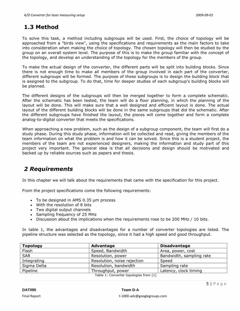
1.3 Method
To solve this task, a method including subgroups will be used. First, the choice of topology will be
approached from a "birds view", using the specifications and requirements as the main factors to take
into consideration when making the choice of topology. The chosen topology will then be studied by the
group on an overall system level. The purpose of this is to make the group familiar with the concept of
the topology, and develop an understanding of the topology for the members of the group.
To make the actual design of the converter, the different parts will be split into building blocks. Since
there is not enough time to make all members of the group involved in each part of the converter,
different subgroups will be formed. The purpose of these subgroups is to design the building block that
is assigned to the subgroup. To do that, time for deeper studies of each subgroup's building blocks will
be planned.
The different designs of the subgroups will then be merged together to form a complete schematic.
After the schematic has been tested, the team will do a floor planning, in which the planning of the
layout will be done. This will make sure that a well designed and efficient layout is done. The actual
layout of the different building blocks will be done in the same subgroups that did the schematic. After
the different subgroups have finished the layout, the pieces will come together and form a complete
analog-to-digital converter that meets the specifications.
When approaching a new problem, such as the design of a subgroup component, the team will first do a
study phase. During this study phase, information will be collected and read, giving the members of the
team information on what the problem is and how it can be solved. Since this is a student project, the
members of the team are not experienced designers, making the information and study part of this
project very important. The general idea is that all decisions and design should be motivated and
backed up by reliable sources such as papers and thesis.
2 Requirements
In this chapter we will talk about the requirements that came with the specification for this project.
From the project specifications come the following requirements:
To be designed in AMS 0.35 μm process
With the resolution of 8 bits
Two digital output channels
Sampling frequency of 25 MHz
Discussion about the implications when the requirements rose to be 200 MHz / 10 bits.
In table 1, the advantages and disadvantages for a number of converter topologies are listed. The
pipeline structure was selected as the topology, since it had a high speed and good throughput.
Topology Advantage Disadvantage
Flash Speed, Bandwidth Area, power, cost
SAR Resolution, power Bandwidth, sampling rate
Integrating Resolution, noise rejection Speed
Sigma Delta Resolution, bandwidth Sampling rate
Pipeline Throughput, power Latency, clock timing Table 1: Converter topologies from [1]
A/D Converter for laser measuring setup 2009‐09‐01
6 | P a g e
DAT095 Team D‐A
Final Report t‐1000‐[email protected]
3 Design Considerations
For the pipeline structure, a number of design considerations needs to be taken into account. The
specifications clearly states the requirements for the converter, but to meet these requirements, the
different things need to be taken into account when designing the different blocks. In this chapter we
discuss the theory behind each sub-block and what need to be considered when designing the different
sub-blocks.
3.1 System Level
The following section contains an explanation of the theory behind subranging converters, and what
needs to be considered when designing one.
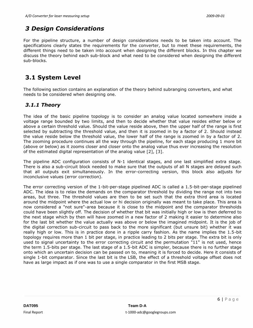
3.1.1 Theory
The idea of the basic pipeline topology is to consider an analog value located somewhere inside a
voltage range bounded by two limits, and then to decide whether that value resides either below or
above a certain threshold value. Should the value reside above, then the upper half of the range is first
selected by subtracting the threshold value, and then it is zoomed in by a factor of 2. Should instead
the value reside below the threshold value, the lower half of the range is zoomed in by a factor of 2.
The zooming procedure continues all the way through the pipeline, for each stage producing 1 more bit
(above or below) as it zooms closer and closer onto the analog value thus ever increasing the resolution
of the estimated digital representation of the analog value [2], [3].
The pipeline ADC configuration consists of N-1 identical stages, and one last simplified extra stage.
There is also a sub-circuit block needed to make sure that the outputs of all N stages are delayed such
that all outputs exit simultaneously. In the error-correcting version, this block also adjusts for
inconclusive values (error correction).
The error correcting version of the 1-bit-per-stage pipelined ADC is called a 1.5-bit-per-stage pipelined
ADC. The idea is to relax the demands on the comparator threshold by dividing the range not into two
areas, but three. The threshold values are then to be set such that the extra third area is located
around the midpoint where the actual low or hi decision originally was meant to take place. This area is
now considered a "not sure"-area because it is close to the midpoint and the comparator thresholds
could have been slightly off. The decision of whether that bit was initially high or low is then deferred to
the next stage which by then will have zoomed in a new factor of 2 making it easier to determine also
for the last bit whether the value actually was above or below the imagined midpoint. It is the job of
the digital correction sub-circuit to pass back to the more significant (but unsure bit) whether it was
really high or low. This is in practice done in a ripple carry fashion. As the name implies the 1.5-bit
topology requires more than 1 bit per stage, in practice leading to 2 bits per stage. The extra bit is only
used to signal uncertainty to the error correcting circuit and the permutation "11" is not used, hence
the term 1.5-bits per stage. The last stage of a 1.5-bit ADC is simpler, because there is no further stage
onto which an uncertain decision can be passed on to, meaning it is forced to decide. Here it consists of
single 1-bit comparator. Since the last bit is the LSB, the effect of a threshold voltage offset does not
have as large impact as if one was to use a single comparator in the first MSB stage.

A/D Converter for laser measuring setup 2009‐09‐01
7 | P a g e
DAT095 Team D‐A
Final Report t‐1000‐[email protected]
Figure 1: Block diagram of pipelined 1.5-bit ADC
Figure 2: Block diagram of 1 stage in the pipeline
The pipeline is driven by a clock and its non-overlapping inverses (phi1 and phi2) as shown in Figure 4.
Consecutive pipeline stages are triggered by opposite clock-phases so that some data is always clocked
out of the pipeline sub-circuit every half period. This means that the delays in the digital-correction
circuit needs to be wired in such a way that every other delay chain is offset by half a period. This
ensures that the data bits that belong together will be output at the same instant, as shown in
figure 13. A new data word is thus complete for each clock cycle, and the latency added by the pipeline
for an 8-bit result becomes 4 clock cycles.

A/D Converter for laser measuring setup 2009‐09‐01
8 | P a g e
DAT095 Team D‐A
Final Report t‐1000‐[email protected]
Figure 3: 1.5-bit stage residue input/output characteristics
The input/output characteristic for each single 1.5-bit stage is described in Figure 3. The input (x-axis)
is mapped to an output (y-axis). The slope is always 2/1 because of the zooming amplification at the
end of each stage. The input is equal to two times the output except when the input trips any of the
comparator threshold values. Then the input is either subtracted (exceeds high threshold) or added
(subceeds low threshold) by 1/4*2=1/2 of the small signal voltage swing.

A/D Converter for laser measuring setup 2009‐09‐01
9 | P a g e
DAT095 Team D‐A
Final Report t‐1000‐[email protected]
Figure 4: 10 MHz non-overlapping clocks simulated using transient analysis
The function of the single 1.5-bit stage is illustrated in Figures 5 and 6 below [3]. Firstly, as shown in
Figure 5, clock phi1 is high (phase 1) and the input is applied to the stage already when the opamp of
the last stage is still in operation. The sampling capacitors then follow the input because they are
grounded and can accept charge. The input is also routed to the comparators which decide whether the
input is above or below their respective threshold value. The comparator digital outputs are then
recoded and latched at the end of the first phase according to table 2 below. Also at the end of the first
phase the sampling is performed. The actual sampling instant is when the clock designated phi1prim
goes low cutting off the connection to ground, thus making it impossible to charge the capacitor any
further. An instant later clock phi1 also goes low, disconnecting the capacitors from the input and then,
as clock phi2 goes high, reconnecting them to the multiplexer and the feedback path, hereby
proceeding to phase 2, as indicated by Figure 7. This phase establishes a times-two amplification once
the opamp has settled (supposedly) sometime before clock phi2prim has gone low and the next stage
samples. Note again that the next stage is already at this time following the input from the current
stage’s output, because phi2 controls the input switch to the next stage. Also consider that each stage
does nothing else than follows the input for most of the time during phase 1 when the preceding stage
is busy settling.

A/D Converter for laser measuring setup 2009‐09‐01
10 | P a g e
DAT095 Team D‐A
Final Report t‐1000‐[email protected]
Figure 5: Single-ended switched-capacitor operation of single 1.5-bit pipeline stage during phase 1
Figure 6: Single-ended switched-capacitor operation of single 1.5-bit pipeline stage during phase 2
Comparator value [bottom,
top]
Recoded value [bit0, bit1] Comment
11 10 certain 1
10 01 not sure
00 00 certain 0
01 X supposedly not possible Table 2: Comparator recoding scheme

A/D Converter for laser measuring setup 2009‐09‐01
11 | P a g e
DAT095 Team D‐A
Final Report t‐1000‐[email protected]
Although Figures 5 and 6 are shown conceptually as single-ended, all real analog signal paths need to
be differential in the final chip realization to reduce common-mode disturbances commonly caused by
clocks and other kinds of switching-activity. These disturbances are believed not to be an issue
regarding digital signals which are all single-ended. Refer to appendix A for information on the
differential signal conventions used in this project.
To simulate and understand the timing between the different blocks, we created a Simulink model of
the converter. The model used non-overlapping clocks, and gave us good insight into how the complete
system works.
Figure 7: Stage clocking

A/D Converter for laser measuring setup 2009‐09‐01
12 | P a g e
DAT095 Team D‐A
Final Report t‐1000‐[email protected]
3.1.2 Considerations
When designing an 8-bit pipeline ADC according to the specifications, the main consideration on a
system level is the clock speed. Since the converter is set to work at 25 MHz, new data must be
sampled into the converter every 40 ns. This means that the stages of the pipeline must work in
25 MHz cycles. Since the stages are overlapped this gives each stage a total time of 20 ns from
sampling to the time that the data must be ready for the next stage. Settling time of the opamp and
other factors eventually put a boundary to at what rate the circuit can actually be clocked.
3.2 Sub-ADC
The Sub-ADC which is discussed here refers to the block called ADC in Figure 2.
3.2.1 Theory
As shown in Figure 2, the main part of the 1.5bits sub-ADC cell is the comparator.
A comparator is used to compare two analog inputs voltages and output a high voltage level or a low
voltage level which can be used to generate the logic outputs later. The comparator can be seen as
the bridge between an analog circuit and a digital circuit.
The ideal comparator character is that when input voltage Vin larger than (or equal to) the reference
voltage Vref, Vout should pull up to high voltage level; when Vin smaller than the reference voltage
Vref, Vout should pull down to low voltage level. That is:
However, due to practical considerations, the real comparator has to be:
Av is the gain of the comparator
The comparator character leads to a high gain requirement. Higher gain can reduce the demand for
differential input which makes the output change from high voltage level to low voltage level and vice
versa. In other words, high gain is the key requirement to improve the sensitivity and the speed.
A/D Converter for laser measuring setup 2009‐09‐01
13 | P a g e
DAT095 Team D‐A
Final Report t‐1000‐[email protected]
Frequency compensation is not needed since comparator is the largest signal application of an
amplifier, that is, the system always works in open loop.
In addition, a high voltage swing is important as well, since the output should be the high voltage
level or the low voltage level of the system.
A latch is used to achieve a stable output and to enlarge the voltage difference between the high
voltage level and the low voltage level.
To generate the threshold voltage and compare the input voltages with the threshold voltage, two
switched capacitors with a certain ratio are used.
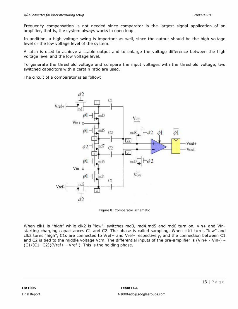
The circuit of a comparator is as follow:
Figure 8: Comparator schematic
When clk1 is “high” while clk2 is “low”, switches md3, md4,md5 and md6 turn on, Vin+ and Vin-
starting charging capacitances C1 and C2. The phase is called sampling. When clk1 turns “low” and
clk2 turns “high”, C1s are connected to Vref+ and Vref- respectively, and the connection between C1
and C2 is tied to the middle voltage Vcm. The differential inputs of the pre-amplifier is (Vin+ - Vin-) –
(C1/(C1+C2))(Vref+ - Vref-). This is the holding phase.
A/D Converter for laser measuring setup 2009‐09‐01
14 | P a g e
DAT095 Team D‐A
Final Report t‐1000‐[email protected]
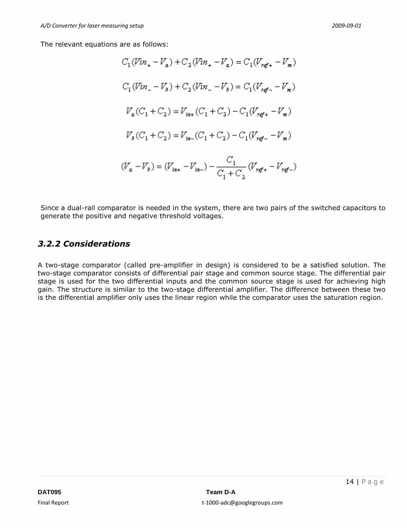
The relevant equations are as follows:
Since a dual-rail comparator is needed in the system, there are two pairs of the switched capacitors to
generate the positive and negative threshold voltages.
3.2.2 Considerations
A two-stage comparator (called pre-amplifier in design) is considered to be a satisfied solution. The
two-stage comparator consists of differential pair stage and common source stage. The differential pair
stage is used for the two differential inputs and the common source stage is used for achieving high
gain. The structure is similar to the two-stage differential amplifier. The difference between these two
is the differential amplifier only uses the linear region while the comparator uses the saturation region.

A/D Converter for laser measuring setup 2009‐09‐01
15 | P a g e
DAT095 Team D‐A
Final Report t‐1000‐[email protected]
Figure 9: Pre-amplifier schematic
Appropriate values of the current and the ratio of the length and width of the two transistors of
differential pair are keys when considering the voltage gain, since decreasing the current from current
source or enlarging the ratio leads to the voltages gain increasing and the linear region diminishing.
The common source stage is designed for higher voltage gain.
To solve the problem of body effect, pmos type differential pair is used in design.
To match this, an nmos type latch is used in this system, so that a current path exists from pmos in
the common source stage to the nmos in latch when the clocked transistor switch shut down.
Figure 10: Latch schematic
A/D Converter for laser measuring setup 2009‐09‐01
16 | P a g e
DAT095 Team D‐A
Final Report t‐1000‐[email protected]
The capacitances of the switched capacitors are calculated according to the equations shown above.
Since the last stage is actually the one bit ADC, both positive threshold and negative threshold should
merge to 0 volt. In order to keep the similar structure so that the layout can be reused, one of the
capacitors in both positive capacitor pair and negative capacitor pair are set to be small enough to
make the two thresholds close enough to 0 volt.
Clock is also considered in ADC design. The clock applied to latch should be the inversion of the one
applied to pre-amplifier. The clocked transistor switches should be applied to the common source stage
rather than differential pair stage, since there should be the current path from Vdd to Vss when the
two transistors shut down.
3.3 Sub-DAC
The DAC function is closely integrated into the stage together with the ADC and the opamp. The
concept is depicted in Figures 5 and 6 above.
3.3.1 Theory and considerations
The function of the DAC block is to use a digital value to subtract the correct analog value from the
sampling capacitors inside the stage.
For the switching/subtracting operations in the DAC, C-switches were used to minimize influence of
asymmetric voltage characteristics compared with using single transistors. Possibly single N-transistor
could have been enough because the swing does not use the full voltage range, but that was never
investigated more closely.
3.4 Opamp
The purpose of the opamp in the circuit is multiplying the residue signal with 2 to restore the signal
level back to the original swing. The place of the opamp can be observed from Figures 5 and 6.
3.4.1 Theory
When choosing topology for the opamp, we mainly considered speed. Table 3 from [4] shows 4
different topologies and their properties. The fastest opamp is the telescopic topology. However, the
telescopic topology suffers from low voltage swing. It is not a top priority for this project to have a high
voltage swing; however, the folded-cascode topology was selected as the opamp topology for this
project. The folded-cacscode has a high speed and medium voltage swing, which makes it suitable for
the project. The folded-cascode topology is found in Figure 11.

A/D Converter for laser measuring setup 2009‐09‐01
17 | P a g e
DAT095 Team D‐A
Final Report t‐1000‐[email protected]
Gain Output
Swing
Speed Power
Dissipation
Noise
Telescopic Medium Medium Highest Low Low
Folded
Cascode
Medium Medium High Medium Medium
Two Stage High Highest Low Medium Low
Gain Boosted High Medium Medium High Medium
Table 3: Opamp topologies
Figure 11: Folded-cascode schematic
To calculate the theoretical voltage swing, the formulas below are used. The voltage drops over the
lower and upper transistors are calculated. These voltages are then subtracted from the total supply
voltage, leaving the total voltage swing.
A/D Converter for laser measuring setup 2009‐09‐01
18 | P a g e
DAT095 Team D‐A
Final Report t‐1000‐[email protected]
Lower end: (Vgs3/4-Vt3/4)+ (Vgs5/6-Vt5/6)
Upper end: Vdd – ( |(Vgs7/8-Vt7/8)|+ |(Vgs9/10-Vt9/10)|)
Total peak to peak: Vdd – ( |(Vgs7/8-Vt7/8)|+ |(Vgs9/10-Vt9/10)| + (Vgs3/4-Vt3/4)+
(Vgs5/6-Vt5/6))
The frequency response is dominated by the pole at the output which is the combination of load
capacitance and the output resistance where the output resistance is approximately:
Gain is based on transconductance and output resistance:
The gain can be increased by using NMOS input transistors to take advantage of higher mobility of
electrons however this lowers the pole in the nodes X and Y.
Common-mode feedback (CMFB) is necessary in fully differential amplifiers since the common-mode
level is very sensitive to mismatches and it can not be set via differential feedback. The difference
between the output nodes should be sensed via a sensing circuitry and then fed back to the appropriate
biasing node in order to put the amplifier output back on the desired dc points.
The sensing circuitry can be designed with resistors, transistors or capacitors. In resistor-based design,
the resistance values must be high enough in order to avoid causing a decrease in gain. This gives very
large resistance values that are on the order of mega ohms which are not very cheap to produce in
reality. Source followers can be added to decrease the amount of required resistance. However they
cause a drop in maximum available voltage swing. In this project, we use capacitors in switched-
capacitor mode with two capacitors that are pre-charged to desired value controlling bias of the
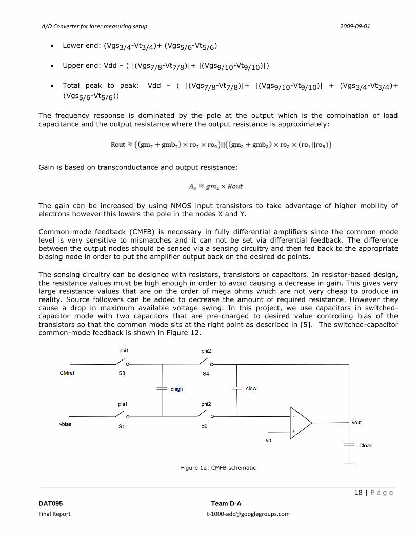
transistors so that the common mode sits at the right point as described in [5]. The switched-capacitor
common-mode feedback is shown in Figure 12.
Figure 12: CMFB schematic
A/D Converter for laser measuring setup 2009‐09‐01
19 | P a g e
DAT095 Team D‐A
Final Report t‐1000‐[email protected]
3.4.2 Considerations
The main consideration for the opamp is the speed and the exact gain of 2. Using a switched capacitor
CMFB we will make sure that the outputs are around the common mode. The timing of the switches in
the CMFB will make the CMFB operate when the opamp is not operating.
With the folded-cascode architecture, the theoretical voltage swing depends on the overdrive voltages
of the upper and lower transistors in the output stage. These should be as small as possible to give a
large voltage range. However, the sizes of the transistors are dependent on the overdrive voltages and
the drain current. When increasing the overdrive voltages and keeping the size of the transistor fixed,
one enables a larger current to pass through the transistor. A tradeoff between transistor size and
voltage swing must be made. Choosing overdrive voltages between 0.2-0.3, we arrive at a large
enough voltage swing and the transistors are kept to a reasonable size.
A high open-loop gain is needed to avoid nonlinearities in the opamp. When designing the folded-
cascode opamp, an open-loop gain of around 80 dB is desirable. Since the opamp must be fast, a high
slew rate at the output is desired. 1 pF loads was used during calculations, with feedback capacitances
of 1.8 pF. We chose 1 pF to make the design comparable to our previous opamp-design assignments.
However our approach was not the most successful.
To meet the requirements, the settling time of the opamp is more important to the project than the
bandwidth. Since the input to the opamp will be a sampled signal, the input will be constant during the
whole phase, and the performance will depend on the settling time. The stage will operate in 40ns, but
the opamp needs to settle within 20 ns to meet the requirements. However, the actual settling time is
smaller, around 10-15ns due to settling of input signal and other factors.
Since the gain of the opamp is defined by the relations between the capacitors in the feedback, the
ratio between them must be very well matched. To define an accurate gain, square unit capacitors are
used with a size that guarantees that the relative matching is 99.99%.
To meet the requirements on speed, preliminary calculations on speed and slew rate gave a
recommended bias current ib of around 350 mA. The calculations were made by approximately dividing
the time budget between circuit blocks. To squeeze even more out of the amplifier, even higher
currents were tested. The tradeoff in this case is between speed and transistor sizes. Small transistors
give smaller parasitics and are smaller in layout. However, larger transistors are needed to handle the
drain current. Drain current of 400 mA, 500 mA and 600 mA were examined. However, the advantage
of going from 400mA to 500mA is extremely small in comparison to the increased transistor sizes.
When going to 600mA, the transistors became so large that the parasitics clearly affected the speed of
the opamp.

A/D Converter for laser measuring setup 2009‐09‐01
20 | P a g e
DAT095 Team D‐A
Final Report t‐1000‐[email protected]
3.5 Delay and Digital Correction
The delay and correction circuit block works according to Figure 13 below.
3.5.1 Theory
By delaying the output from the initial stage with seven delays and so on, one makes sure that the
output from all the stages will be passed on to the digital correction part at the same instant. In the
correction part, an undecided stage is decided by receiving the carry from the lower-bit stage. The
thresholds should be set to 1/4 of the reference voltage (3/8 and 5/8 of the total swing). In this case,
the stage after the undecided stage can never manage to amplify the new residue above or below
2/4=1/2, meaning that the output of the next stage will certainly be either below 0 (undecided stage
residue above 0) or above 0 (undecided stage residue below 0). Note that if the undecided stage
instead would have been decided, it would have amplified only the upper or lower half of the residue to
start with. The idea is illustrated in [2] page 17.
Figure 13: Delay and digital correction concept circuit
A/D Converter for laser measuring setup 2009‐09‐01
21 | P a g e
DAT095 Team D‐A
Final Report t‐1000‐[email protected]
3.5.2 Considerations
The digital correction and delay part does not pose any dire timing requirements when running at a
clock frequency of less than or equal to 25 MHz. Instead the primary design goal for this circuit is that it
should function reliably and present an as small a load as possible to the clock drivers. A secondary
design goal is to minimize the area. The delay-correction block is clocked by clocks Phi1prim and
Phi2prim, outputting data at an integer number of half clock cycles from the sampling instant. The
decision to use the delayed prim clocks instead of the standard clocks was a design decision that has
the advantage of spreading the total load onto different clock buffers.
4 Converter Blocks, Theory and Simulation Results
In this chapter we will discuss the results we got during the simulations of the different circuits.
When designing the converter, we developed and tested the different blocks of the converter
separately. We made decisions about timing and voltages in advance, to make sure that the blocks
would fit together in a good way. After the different blocks had been tested, they were put together to
form the complete converter system, and then the whole system was finally tested and verified as a
unit.
4.1 System Level
The converter was assembled piece by piece. All blocks were tested separately, and then put together
to form the entire pipeline. This was done first on a schematic level. When the system was working on a
schematic level, all the blocks were laid out. All blocks were again tested separately after being laid out.
After that, all blocks were assembled again and post-layout simulations were run.
The requirements of the project states that the speed of the converter should be 25MHz. However,
when the entire ADC was assembled at a schematic level, it became clear that the settling time of the
system was longer than expected. The output of each stage did not settle within an acceptable level,
and therefore the outputs of the entire ADC were wrong. To remedy this problem, all blocks were
revisited. Small changes were made in the opamp and in the sub-ADC to make them faster. However,
when assembling the ADC again, the stage still could not settle. Therefore we made the decision to
lower the clock frequency. Instead of making the system run at the desired 25 MHz, the group decided
together with the project director to aim for a lower clock frequency. The reason for this decision is that
the group wanted to continue with the project and go on to layout.
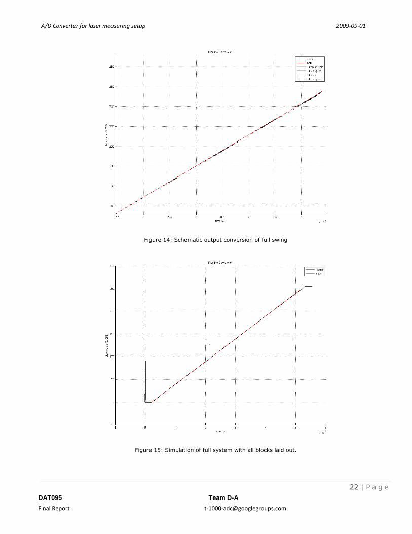
To test the whole converter, a simulation using a ramp input was used. As input, a ramp that covers
the whole input range was used, implying that the entire output range ought to be covered smoothly.
In Figure 14 a piece of the ramp simulated using schematics is seen. The figure shows how the
converter follows the input. The step size of the output is not perfect, however a part of this is due to
timing problems between the ramp input signal and the sampling of the converter.
A/D Converter for laser measuring setup 2009‐09‐01
22 | P a g e
DAT095 Team D‐A
Final Report t‐1000‐[email protected]
Figure 14: Schematic output conversion of full swing
Figure 15: Simulation of full system with all blocks laid out.

A/D Converter for laser measuring setup 2009‐09‐01
23 | P a g e
DAT095 Team D‐A
Final Report t‐1000‐[email protected]
4.2 Sub-ADC
The main part of Sub-ADC cell is implemented as pre-amplifier followed by a latch. The pre-amplifier
consists of two differential stages followed by a common source stage.
Switched capacitors are used to sample the input voltages and generate the threshold voltages. All the
ratios of capacitors are the same except the ones in the last stage. Since the output should be decided
by the last stage finally, one bit ADC cell is needed here. To avoid the different structure from other
stages, in the one bit ADC cell, only the ratio of capacitors changed but still two comparators are used
rather than one. To implement that, the threshold voltages should be close to 0 volt as much as
possible. One capacitor of the pair (That is C2 in Figure 8) need to be very small. Considering the
capacitor size limitation in layout implementation, 3.4 fF capacitors are selected for the one bit ADC
cell.
The schematics and layouts are shown as follow.
Figure 16: Schematic of Pre-amplifier
A/D Converter for laser measuring setup 2009‐09‐01
24 | P a g e
DAT095 Team D‐A
Final Report t‐1000‐[email protected]
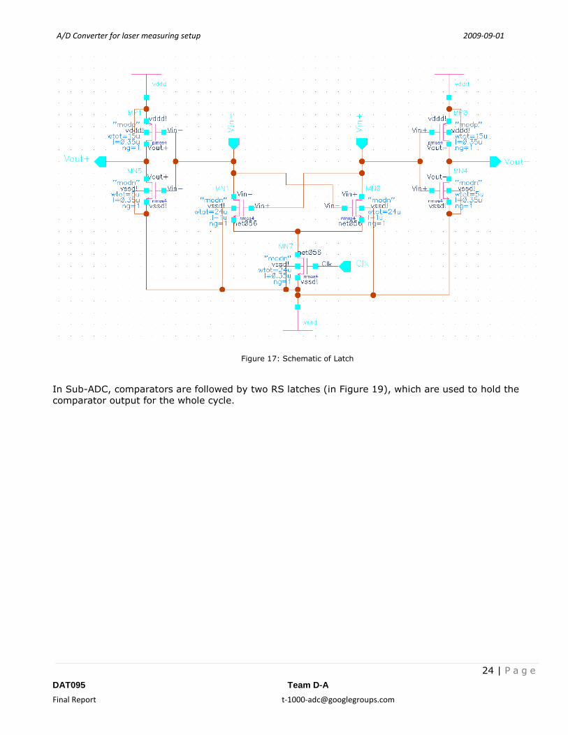
Figure 17: Schematic of Latch
In Sub-ADC, comparators are followed by two RS latches (in Figure 19), which are used to hold the
comparator output for the whole cycle.
A/D Converter for laser measuring setup 2009‐09‐01
25 | P a g e
DAT095 Team D‐A
Final Report t‐1000‐[email protected]
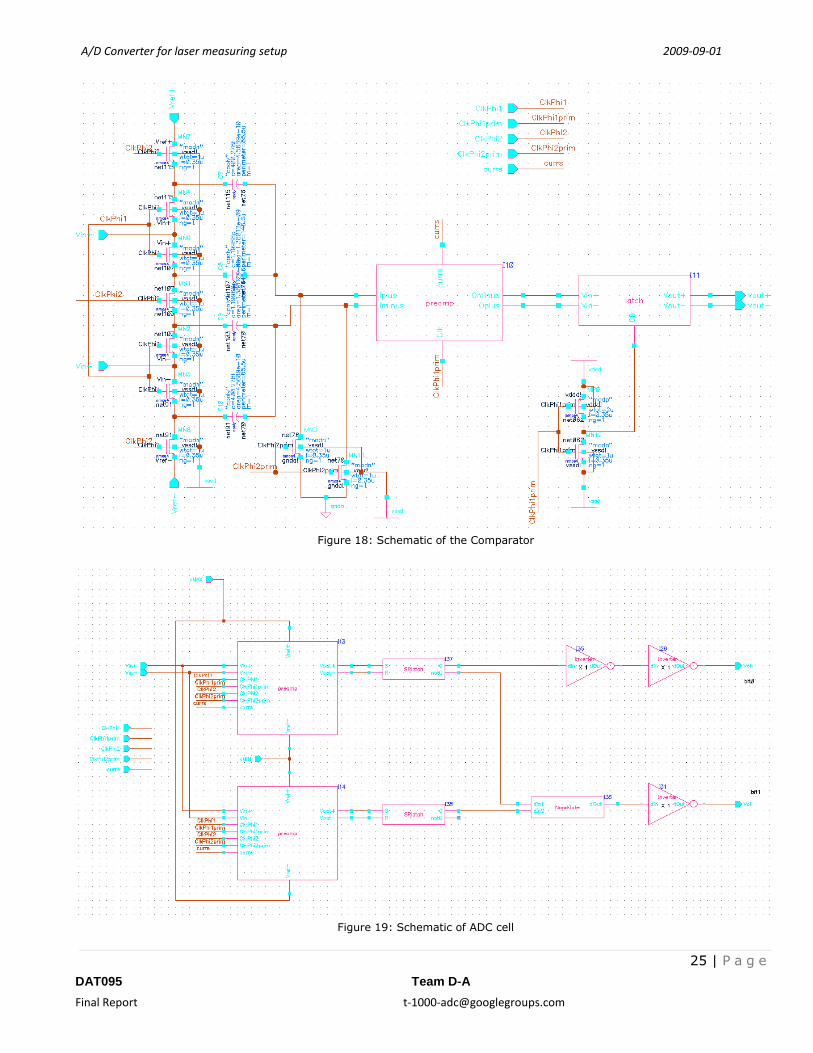
Figure 18: Schematic of the Comparator
Figure 19: Schematic of ADC cell

A/D Converter for laser measuring setup 2009‐09‐01
26 | P a g e
DAT095 Team D‐A
Final Report t‐1000‐[email protected]
Figure 20: Layout of the ADC cell
Figure 21: Layout of ADC cell of the last stage
A/D Converter for laser measuring setup 2009‐09‐01
27 | P a g e
DAT095 Team D‐A
Final Report t‐1000‐[email protected]
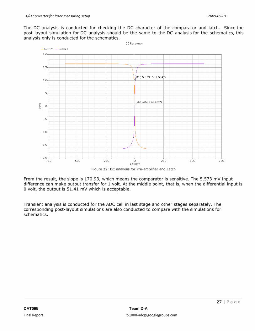
The DC analysis is conducted for checking the DC character of the comparator and latch. Since the
post-layout simulation for DC analysis should be the same to the DC analysis for the schematics, this
analysis only is conducted for the schematics.
Figure 22: DC analysis for Pre-amplifier and Latch
From the result, the slope is 170.93, which means the comparator is sensitive. The 5.573 mV input
difference can make output transfer for 1 volt. At the middle point, that is, when the differential input is
0 volt, the output is 51.41 mV which is acceptable.
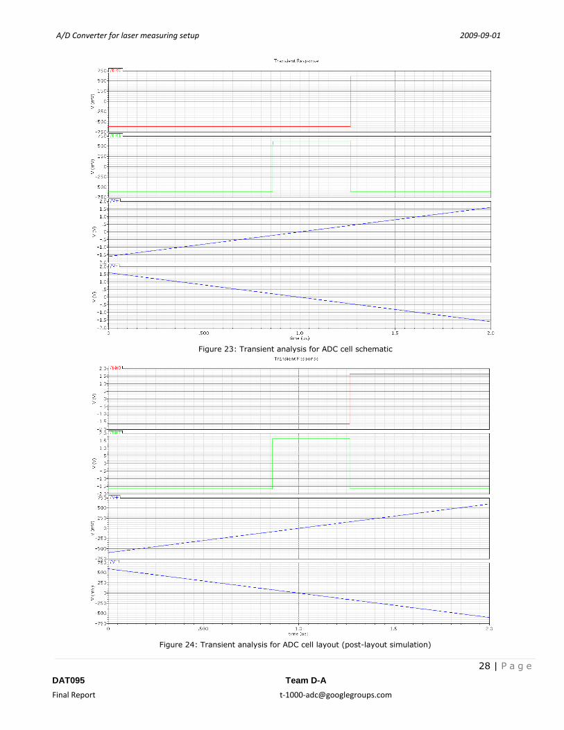
Transient analysis is conducted for the ADC cell in last stage and other stages separately. The
corresponding post-layout simulations are also conducted to compare with the simulations for
schematics.
A/D Converter for laser measuring setup 2009‐09‐01
28 | P a g e
DAT095 Team D‐A
Final Report t‐1000‐[email protected]
Figure 23: Transient analysis for ADC cell schematic
Figure 24: Transient analysis for ADC cell layout (post-layout simulation)
A/D Converter for laser measuring setup 2009‐09‐01
29 | P a g e
DAT095 Team D‐A
Final Report t‐1000‐[email protected]
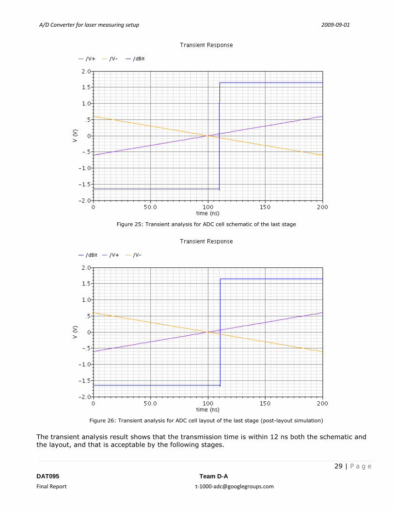
Figure 25: Transient analysis for ADC cell schematic of the last stage
Figure 26: Transient analysis for ADC cell layout of the last stage (post-layout simulation)
The transient analysis result shows that the transmission time is within 12 ns both the schematic and
the layout, and that is acceptable by the following stages.
A/D Converter for laser measuring setup 2009‐09‐01
30 | P a g e
DAT095 Team D‐A
Final Report t‐1000‐[email protected]
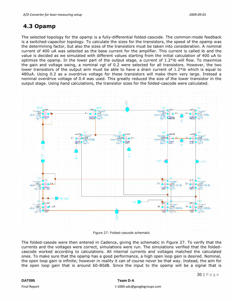
4.3 Opamp
The selected topology for the opamp is a fully-differential folded-cascode. The common-mode feedback
is a switched-capacitor topology. To calculate the sizes for the transistors, the speed of the opamp was
the determining factor, but also the sizes of the transistors must be taken into consideration. A nominal
current of 400 uA was selected as the base current for the amplifier. This current is called ib and the
value is decided as we simulated with different values starting from the initial calculation of 400 uA to
optimize the opamp. In the lower part of the output stage, a current of 1.2*ib will flow. To maximize
the gain and voltage swing, a nominal vgt of 0.2 were selected for all transistors. However, the two
lower transistors of the output arm must be able to have a drain current of 1.2*ib which is equal to
480uA. Using 0.2 as a overdrive voltage for these transistors will make them very large. Instead a
nominal overdrive voltage of 0.4 was used. This greatly reduced the size of the lower transistor in the
output stage. Using hand calculations, the transistor sizes for the folded-cascode were calculated.
Figure 27: Folded-cascode schematic
The folded-casode were then entered in Cadence, giving the schematic in Figure 27. To verify that the
currents and the voltages were correct, simulations were run. The simulations verified that the folded-
cascode worked according to calculations. All internal currents and voltages matched the calculated
ones. To make sure that the opamp has a good performance, a high open loop gain is desired. Nominal,
the open loop gain is infinite; however in reality it can of course never be that way. Instead, the aim for
the open loop gain that is around 60-80dB. Since the input to the opamp will be a signal that is
A/D Converter for laser measuring setup 2009‐09‐01
31 | P a g e
DAT095 Team D‐A
Final Report t‐1000‐[email protected]
sampled, the bandwidth of the opamp is not of great importance.
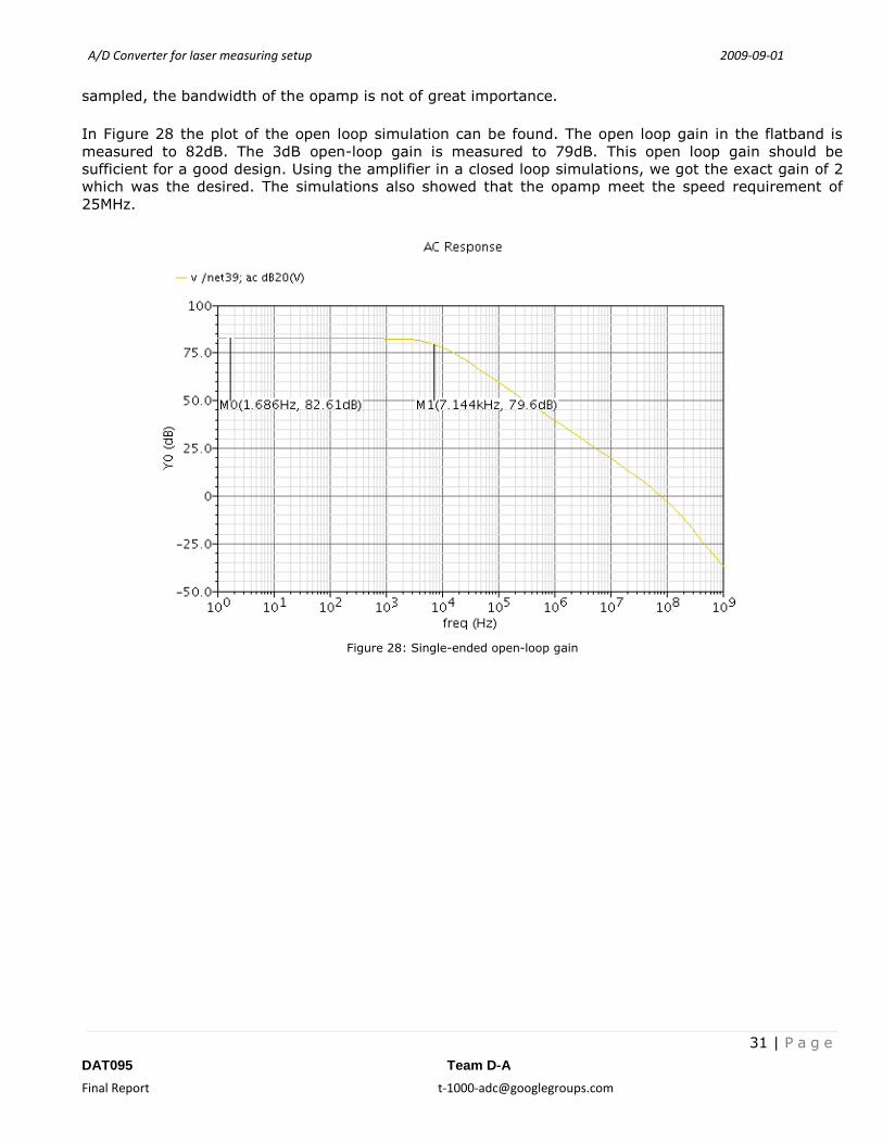
In Figure 28 the plot of the open loop simulation can be found. The open loop gain in the flatband is
measured to 82dB. The 3dB open-loop gain is measured to 79dB. This open loop gain should be
sufficient for a good design. Using the amplifier in a closed loop simulations, we got the exact gain of 2
which was the desired. The simulations also showed that the opamp meet the speed requirement of
25MHz.
Figure 28: Single-ended open-loop gain

A/D Converter for laser measuring setup 2009‐09‐01
32 | P a g e
DAT095 Team D‐A
Final Report t‐1000‐[email protected]
Figure 29: Opamp CMFB schematic

A/D Converter for laser measuring setup 2009‐09‐01
33 | P a g e
DAT095 Team D‐A
Final Report t‐1000‐[email protected]
CMFB [5], was then added to the opamp, see Figure 29. This makes the output of the opamp sit at the
right place, centered around middle of the voltage range which was 0 V for our design as our circuit was
operating between 1.65 V and -1.65 V. The switches in the opamp are regular C-swiches. The CMFB
takes the bias voltage from the opamp in the "vb_out_net". The reference voltage is set in the voltage
source "vb_bias1". Since the output is designed to be centered around 0V, the "vb_bias1" is nominal
0V, or GND. However, since offsets might appear that needs to be cancelled out by the CMFB, a slightly
different voltage might be chosen. Using the CMFB made the output sit at the correct point; however
the gain was no longer 2 but rather 1.999. The speed of the opamp was also lower than without the
CMFB, but the timing requirements were still meet.
When the whole pipeline was put together on a system level, the sizes of the feedback capacitors were
examined. Small capacitors are convenient when making the layout, however due to parasitics; the
feedback capacitors must be large enough to dominate over the parasitics to define the correct gain.
Moreover having large capacitors also decreases the kt/C noise caused by the capacitors. Testing
showed that a size of 600 fF was big enough to define a correct gain. 600 fF is also large enough to
meet the internal desire of 99.99% relative capacitor matching.
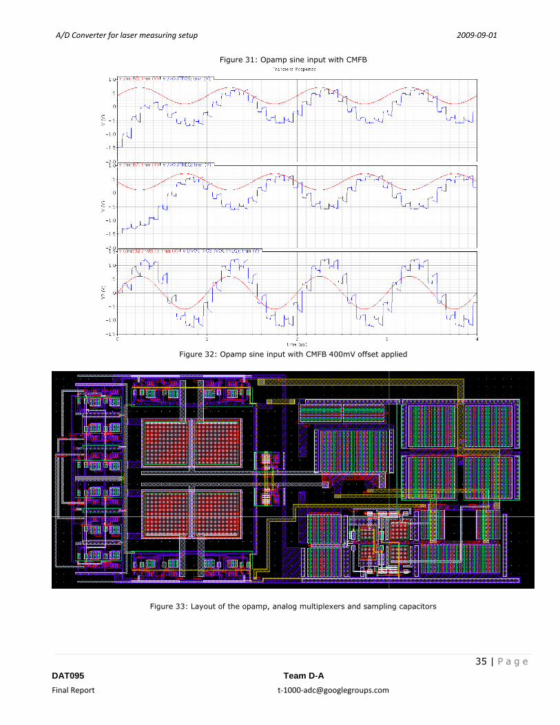
4.4 Sub-DAC and Opamp Block
To further verify that the opamp and the CMFB work, it was put in a configuration together with the
opamp. The schematic is seen in Figure 30. It was then tested within a testbench using a sinusoidal
input. Firstly, a sinusoidal input centered around zero was applied to the testbench. In Figure 31 the
sine input (red) and the output (blue) is visible. The first period of the output signal is wrong, since this
is the warm up time of the system. After that, the output follows the input and everything is correct. To
verify that the CMFB is pulling the outputs back to the common mode 0, the input is offset 400 mV, to
be a sine wave centered around 400mV. In Figure 32 the resulting simulation data is found. The input is
a sine wave with a 400mV offset. The output is a sine wave amplified by 2, but correctly centered
around zero. This is the result of the common mode feedback.

A/D Converter for laser measuring setup 2009‐09‐01
34 | P a g e
DAT095 Team D‐A
Final Report t‐1000‐[email protected]
Figure 30: DAC and opamp schematic
A/D Converter for laser measuring setup 2009‐09‐01
35 | P a g e
DAT095 Team D‐A
Final Report t‐1000‐[email protected]
Figure 31: Opamp sine input with CMFB
Figure 32: Opamp sine input with CMFB 400mV offset applied
Figure 33: Layout of the opamp, analog multiplexers and sampling capacitors
A/D Converter for laser measuring setup 2009‐09‐01
36 | P a g e
DAT095 Team D‐A
Final Report t‐1000‐[email protected]
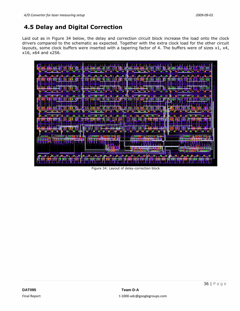
4.5 Delay and Digital Correction
Laid out as in Figure 34 below, the delay and correction circuit block increase the load onto the clock
drivers compared to the schematic as expected. Together with the extra clock load for the other circuit
layouts, some clock buffers were inserted with a tapering factor of 4. The buffers were of sizes x1, x4,
x16, x64 and x256.
Figure 34: Layout of delay-correction block
A/D Converter for laser measuring setup 2009‐09‐01
37 | P a g e
DAT095 Team D‐A
Final Report t‐1000‐[email protected]
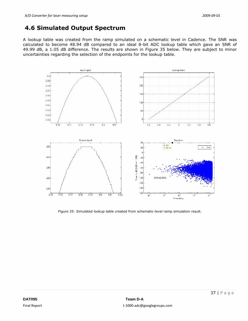
4.6 Simulated Output Spectrum
A lookup table was created from the ramp simulated on a schematic level in Cadence. The SNR was
calculated to become 48.94 dB compared to an ideal 8-bit ADC lookup table which gave an SNR of
49.99 dB, a 1.05 dB difference. The results are shown in Figure 35 below. They are subject to minor
uncertainties regarding the selection of the endpoints for the lookup table.
Figure 35: Simulated lookup table created from schematic-level ramp simulation result.
A/D Converter for laser measuring setup 2009‐09‐01
38 | P a g e
DAT095 Team D‐A
Final Report t‐1000‐[email protected]
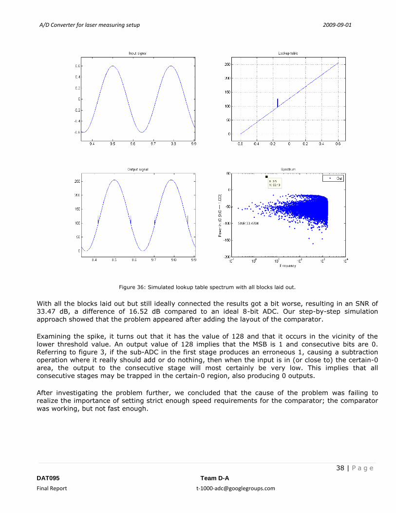
Figure 36: Simulated lookup table spectrum with all blocks laid out.
With all the blocks laid out but still ideally connected the results got a bit worse, resulting in an SNR of
33.47 dB, a difference of 16.52 dB compared to an ideal 8-bit ADC. Our step-by-step simulation
approach showed that the problem appeared after adding the layout of the comparator.
Examining the spike, it turns out that it has the value of 128 and that it occurs in the vicinity of the
lower threshold value. An output value of 128 implies that the MSB is 1 and consecutive bits are 0.
Referring to figure 3, if the sub-ADC in the first stage produces an erroneous 1, causing a subtraction
operation where it really should add or do nothing, then when the input is in (or close to) the certain-0
area, the output to the consecutive stage will most certainly be very low. This implies that all
consecutive stages may be trapped in the certain-0 region, also producing 0 outputs.
After investigating the problem further, we concluded that the cause of the problem was failing to
realize the importance of setting strict enough speed requirements for the comparator; the comparator
was working, but not fast enough.

A/D Converter for laser measuring setup 2009‐09‐01
39 | P a g e
DAT095 Team D‐A
Final Report t‐1000‐[email protected]
Figure 37: Simulated ideal 8-bit ADC spectrum.
5 Discussion
In the previous chapters, the requirements, theory and results this project are presented. In this
chapter we will discuss these results.
5.1 System Level
The main objectives for the converter was that it should use 8 bits with a 25MHz input. The pipeline
that is designed during this project contains 8 bits. But the speed of 25MHz could not be met; instead
we used a speed of 10 MHz. This has been the main concern for this project on a system level.
Attempts to decrease the settling time on a block level have been done, without result. One way to
make the timing requirement on a system level is of course to change to a faster topology, for example
a flash converter. However, with that comes other disadvantages, and since the speed problem was
revealed so late in the project, no attempts to change the topology have been made by the group.

A/D Converter for laser measuring setup 2009‐09‐01
40 | P a g e
DAT095 Team D‐A
Final Report t‐1000‐[email protected]
The results from the simulations show that the overall behavior of the converter is correct. There are
some minor spikes and errors but overall it follows the input. The changes in step size of the output
from the ramp simulation can partially be explained by timing errors between the sample and hold
stage and the input. The ramp is in fact a "stair" with small steps. If the timing is not perfect between
the ramp and the sample and hold, then one value can be sampled twice, resulting in a double value on
the output which is can explain some of the errors in the step size on the output.
5.2 Sub-ADC
Considering about the DC analysis, since in the system, the inputs of the ADC cell would between -
600mV and 600mV, the sweep voltage of the input of the pre-amplifier is set to from -600mV to
600mV. By adjusting the current source and the ratio of the width and length of the transistors of the
differential pair, satisfied outputs are achieved. The intersection of the dual-rail output is almost the 0
volt point so that precise enough decision can be make even the differential voltage between input
voltage and threshold voltage is small. The theoretical threshold voltage is 51.41mV according to the
result of simulation. If 1V is considered to be the voltage that can drive the next stage, then only
differential voltage of 5.573mV is need to achieve such an output. All of this thanks to the large gain of
the two stages amplifier and the latch.
The transient simulation result is depended on the precision of the capacitors. Considering the
capacitors also need to be able to be implemented in layout, the ratio can not be ideal, especially in the
last stage. Considering the balance of the two aspects, in addition, the imprecision is only several
mV, it is acceptable.
The post-layout simulation is OK, since the results are almost the same to the schematics.
5.3 Opamp
The main problems with the opamp during this project have been the gain and the speed. To make the
pipeline architecture work correctly, the gain must be exactly 2. However, after adding the CMFB to the
opamp, the gain dropped to 1.99, which has caused complications during the rest of the project.
However, this problem could not be solved by the group. The CMFB is a switched capacitor common
mode feed back. We have tried different sizes of switches and capacitors, but the results are still the
same. One way to get around this problem could be to try another topology of CMFB topologys.
The speed of the opamp became a problem when assembling the system. When we examined the
opamp on its own, the settling time was acceptable and was within the time budget. However, when
putting it together with the full system, the settling time increased, making it exceed the original time
budget. This problem probably aroused because all the loads became larger than expected when
assembling the system. When simulating the opamp on its own, we used a load of 1 pF. However, this
turned out to be an erronous way to model it. Since the speed depends on the current in the output
stage, a higher current could result in a faster opamp. However, when the current through the
transistors in the output stage increases, the sizes of these transistors increase which also increase the
parasitics of the transistors which may eat up the extra current that is added to the system. So there is
an optimum point where you have small parasitics and large current. To find that point could increase
the performance of the opamp.
A/D Converter for laser measuring setup 2009‐09‐01
41 | P a g e
DAT095 Team D‐A
Final Report t‐1000‐[email protected]
5.4 Sub-DAC and Opamp Block
When putting the opamp together with the DAC, the opamp and the CMFB could be tested in a good
way. When testing the opamp together with the CMFB on its own, it is hard to simulate the switched
feedback. Therefore these pieces were tested together. It became clear that the sizes of the switches in
the feedback clearly affect the speed of the opamp. Before, smaller switches had been used in the DAC,
but when connecting the opamp, larger switches were required to keep the settling time of the opamp
within the time budget. However, when connecting the ADC, the settling time again became longer, and
the adjustments made could not correct it to the right level.
5.5 Delay and Digital Correction
It may have been luxurious to use full D-flipflops instead of just D-latches. Some area and switching
power could possibly have been saved with a simpler latch layout implying no function quality
drawbacks at all.
5.5 Implications of using 10 bits at 200MHz
This project uses 8 bits and 25MHz. But what if the requirements were changed to 10 bits at 200MHz.
Since a pipeline structure is used, the extra 2 bits would not cause any problems since it would only
result in 2 extra stages in the pipeline. However, the speed requirement of 200MHz would most
certainly require a lot of work. Increasing the speed 4 times results in shorter settling time for all
components in the converter. The opamp needs to be faster, and it is uncertain if the folded cascode
can meet that requirement, so another opamp topology might have to be considered.
6 Conclusion
The main goal of this project was to design an 8-bit 25MHz analog to digital converter. It turned out
that the speed requirement could not be meet. Instead a lower clock frequency was selected. In some
cases, the least significant bits are wrong, which results in erroneous conversions, but for the main
case, the ADC can do the conversions with no errors at the lower frequency.
The purpose of this project was for the students to get acquainted with all the things that come from
working in a project and to experience the different trade-offs and design decisions that must be taken
when designing a system from scratch. During the project the group has experienced a lot of these
factors. The timeplan have been revised several times and a decision to lower the frequency has been
made. These are all things that have helped fulfill the purpose of the project. If all things had gone well,
the purpose would not have been fulfilled to the same extent. Therefore it can be concluded that the
purpose of the project have been fulfilled.
For this project we draw the conclusion that the pipeline ADC is a suitable topology for making a
converter that must operate under the conditions given in the specification. The main cause for not
meeting the requirement of 25MHz sampling is that the stages did not have enough time to settle fully,
even though all different parts of the stage looked fine by itself. A more accurate modeling of the loads
could have fixed this problem. The incorrect conversions can be fixed if the gain of the opamp would be
exactly 2.
A/D Converter for laser measuring setup 2009‐09‐01
42 | P a g e
DAT095 Team D‐A
Final Report t‐1000‐[email protected]
When approaching a new problem a method described in chapter 1.3 has been used. This method has
turned out to work well and gave the results that were expected. The design of the schematic took
more time than expected, which rapidly shortened the time for the layout and testing. However, this
was necessary since testing and layout can not be performed if a working schematic is available.
The converter designed in this project does not work perfect, so therefore there is no purpose to use it
in an application where a proper ADC is needed. However, if there are applications where an ADC that
only needs to give rough estimations of the input signal, this converter could be used.
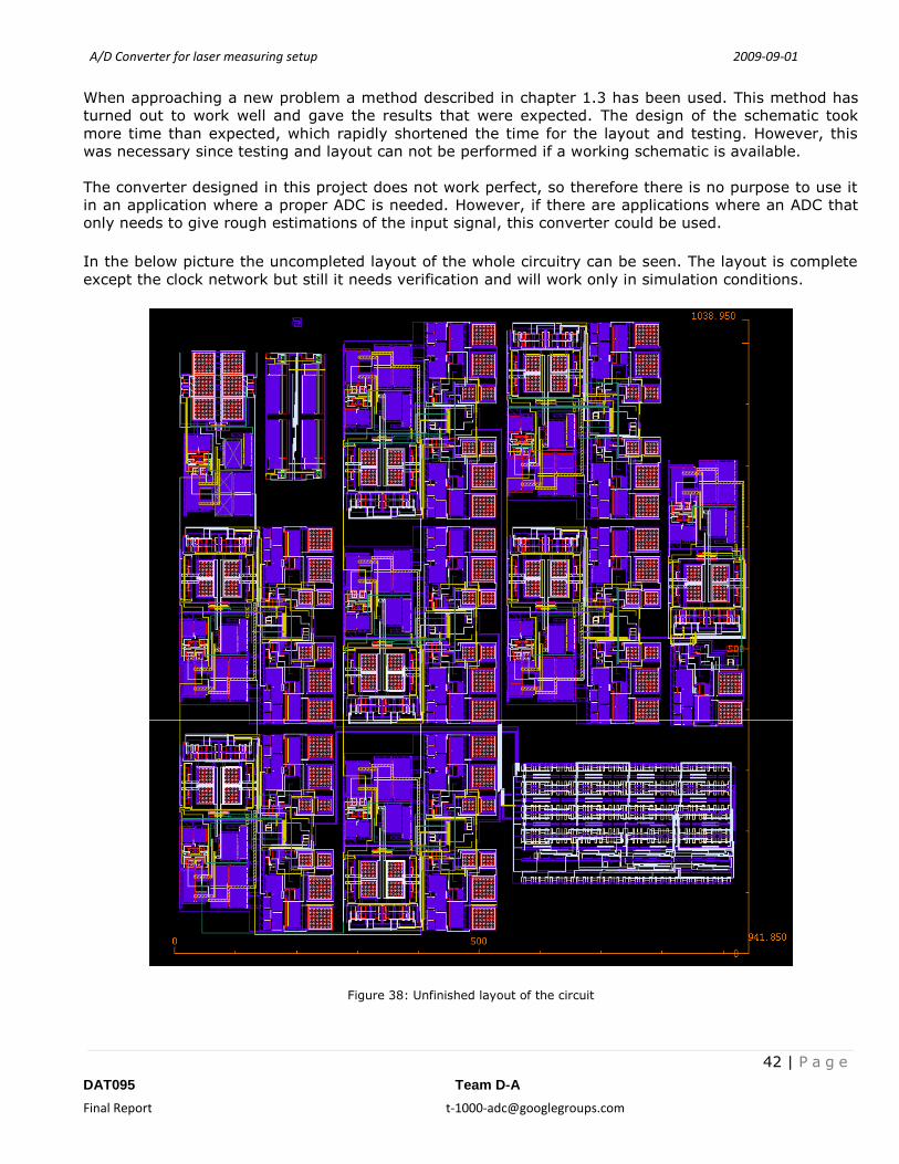
In the below picture the uncompleted layout of the whole circuitry can be seen. The layout is complete
except the clock network but still it needs verification and will work only in simulation conditions.
Figure 38: Unfinished layout of the circuit

A/D Converter for laser measuring setup 2009‐09‐01
43 | P a g e
DAT095 Team D‐A
Final Report t‐1000‐[email protected]
7 Reflections
This project is a student design project at Chalmers University of technology. The purpose of this
project is to give students experience from project work and chip design. Weekly meetings with the
project director have been taking place. During these meeting the group have reported the progress of
the project and had the chance to ask questions regarding the design. Most of the design decisions and
trade-offs have been done by the group. By doing this, the group experienced a top down design flow,
going from specification to layout. This has given the group an experience that will become useful in the
future. Even though the design specifications were not fulfilled, the project was still a success in the
sense that the group have learned a lot from this project.
8 References
[1] Maxim Integrated Products, Appl. Note 634, pp. 1-10.
[2] E. Sanchez,"Pipeline ADC’s", Texas A&M University, Texas, USA, 2000.
[3] A. M Abo, "Design for Reliability of Low Voltage, Switched Capacitor Circuits" Ph.D. dissertation, UC
Berkeley, California, USA, 1999.
[4] B. Razavi, "Operational Amplifiers," in Design of Analog CMOS Integrated Circuts, 2nd ed., New
York: McGRaw-Hill, 2001, pp. 314
[5] O. Choksi, L. R. Carley, Analysis of Switched-Capacitor Common-Mode Feedback Circuit,IEEE
Transactions on Circuits and Systems -II: Analog and Digital Signal Processing, Vol. 50, No. 12,
December 2003.