fine diamonds with laser machining, by c. paul christensen
DESCRIPTION
Of all materials, diamond is harder than any known solid, while also exhibiting the highest values for elastic modulus, atomic density, Debye temperature and thermal conductivity at room temperature. Diamond is chemically inert, and is highly transparent throughout a broad range of the optical spectrum. It is a wide bandgap semiconductor that may be useful at high temperatures or high voltages.TRANSCRIPT
Photonics at Work
Laser Machining
Fine Dialllonds With Laser Machining
UV tools 1/lake quick work of the lvorld:~ hardest Inaterial.
CQ)f all matel1als. diamond . is harder than any
known solid. while also exhibiting the highest values for elas~ tic modulus. atomic denSity. Debye temperature and thennal conductivity at room temperature. Diamond is chemically inert. and Is highly transparent throughout a broad range of the optical spectrum. It Is a wide bandgap semiconductor that may be useful at high temperatures or high voltages.
These properties. along with the ease of growth of diamond Jl1ms by chemical vapor deposition. have made the material desirable for potential applications such as heat spreaders. optical windows. x-ray lithography masks. low-friction and wear-resistant sudaces. cutting-tool coatings and active electronic devices. I
Because of the hardness of dia mond-like materials. mechanical grinding. polishJng and cutting is lime-consuming and costly. Fabrication and shaping problems are compounded by the fact that many potential applications require a high degree of precision and spatial resoluUon. The availability of simple and affordable tecbnJques for shaping and patterning on spatial scales in the micron to millimeter range is expected to sJgnJficantly enhance the utility of diamond as a structural. electroniC and optical material.
The old ways Most current diamond-fabrication
technology has evolved from techn iques used in fabrication of gemstones and diamond tools from naturally occu rring diamond. For the
by C. Paul Christensen
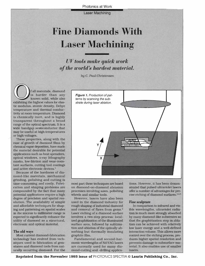
Figure 1. Production of patterns by scanning the substrate during laser ablation.
most part these technJques are based on diamond-on-diamond abrasion processes Involving saw . polishing wheels and similar tools.
However. lasers have also been used in the dJamond lndustry for T0Ugh sha:ping of Industrial diamond and removal of flaws from gems. 2
Laser etching of a diamond surface involves a two-step process: localized graphitization of the illuminated surface area, followed by sublimation and ablation of the optically absorbing but thermally insulating graphite film.
F u ndamental and second-harmornc wavelengths ofNd:YAG lasers are currently used for many diamond-cutting and -drilling appl1ca
tions. However. it has been demonstrated that pulsed ultraviolet lasers offer a number of advantages for precise etching of diamond surfaces.s,u
Fine sculpture In compadson to infrared and vis~
Ible wavelengths. ultraviolet radiation 1s much more strongly absorbed by many ctiamond-Uke substrates so that the graphJtization step in ablation can be achieved with relatively low laser energy and a well-defined Interaction volume. This allows more control over the etching process. produces higher spatial resolution and prevents damage to subsurfac material. It also enables use of smaller lasers.
Reprinted from the November 1993 issue of PHOTONICS SPECTRA © Laurin Publishing Co., Inc.

Photonics at Work
Laser Machining
into a diamond substrate withou t an intennediate mask-generation step.
During the raster motion, the laser output is gated on and off to produce the desired geometry. U e of a CAD/CAM program as a graphical interlace allows long sequences of motion commands associated with complex shapes to be generated with a minimal amount of programming.
Since the time needed to generate a pattern is proportional to the laser pulse repetition rate, most practical tools will incorporate a high-repetition -rate laser.
Ablation depth is cGntrolled by varying the X and Y step size between laser pulses and by adjusting the laser fluence. As s uccessive laser pulses are overlapped on the worksurface during
Figure 2. Laser micromachining configuration. scarmlng. the net exposure of any area become proportional to the spatially
Small ultraviolet lasers can shape lion. The typical 50-}JJ output of a averaged fluence of the focused beam. diamond surfaces with very high pre wavegUide KrF laser focused by an Consequen tly. pulse overlap can be cision and spatial resolution. These optic with numerical aperture of 0.5 used to reduce the effect of beam "hot optical tools combine the small laser will produce a focal spot of 15 to 20- spots- and reduce or eliminate the sources with high-resolUtion imaging }Jm diameter and corresponding flu need for beam homogenization. and precision motion-control systems ence of 10 to 20 J/cm2 • Appropriate The equipment configuration used for sculpting. planarlzing. marking and beam-delivery optics ca n produce for diamond micromachining at patterning of diamond and dlamond smaller spots of the same fluence by Potomac PhotOniCS is shown in Figure like materials. Applications for tools of imaging of the apertured beam. 2 . A waveguide KeF laser producing this type are pervasive, extending from 50- l-hl pulses of 80-ns duration at production of three-dimensional mi Computer control pulse repetition rates eJ!..i.ending to 2 croparts to sculpting likenesses ofAunt Raster or serpentine scanning of kHz i used as the optical source. The Martha·s grandchildren on a facet of the substrate under the focused bean1 laser emission is shaped and coIliher wedding ring. is a simple technique that allows ar mated by beam-delivery optics and
The tluence required for ablation bitrary shapes to be drawn using a focused onto a worksurface with a of diamond materials varies widely CAD/CAM program and then etched UV-transmilUng microscope objecwith the purity of the material and tile wavelength of the laser source. In general. fluences between 0.1 and 10 J/cm2 are required for ablation at ultraviolet wavelengths. Singlepulse ablation depth in diamond is typically a few tens of nanometers. This suggests that precise depth control should be poSSible 10 UV-laserablated microstructures.
Laser-energy requirements are a function of the area of laser focal spot on the worksurface. Beam divergence is also an important parameter that influences the minimum focal spot size and achievable "uence. On micron spatial scales. only a few microjoules of UV laser energy are needed to produce the Ouence levels required for ablation of diamond materials.
Consequently. small UV sources. suchas waveguide excimer lasers. are desirable for microstructure fabrica-
Computer and Stage Controller
Video Camera and Viewing Optics
X-Y-Z Stages
Figure 3. Gear structure formed in the surface of a polished type Ib diamond substrate by 248-nm laser ablation.
Photonics at Work
tive. The objective also images the interaction region onto a high-resolution video camera to allow the operator to closely monitor the machining process.
The workpiece is mounted on precision X-V stages driven by DC motors, and stage position is monitored by encoders. Computer control of stage velocity is carried out using CAD/CAM software, and laser pulsing is synchronized to stage motion.
Almost any shape Figure 3 shows an example of a di
amond gear structure produced by the raster scanning technique. The gear is 300 pm in diameter and is fabricated on the surface of a 0.3 X
1.5-mm chip of type Ib diamond . Depth of the relief around the gear is approximately 50 pm.
The structure was formed using a laser focal spot diameter of 10 pm and a fluence of 5J/cm2 • The gear shown in Figure 3 is not released from the substrate as a separate component. However, a released structure could be formed by simply using a thinner substrate.
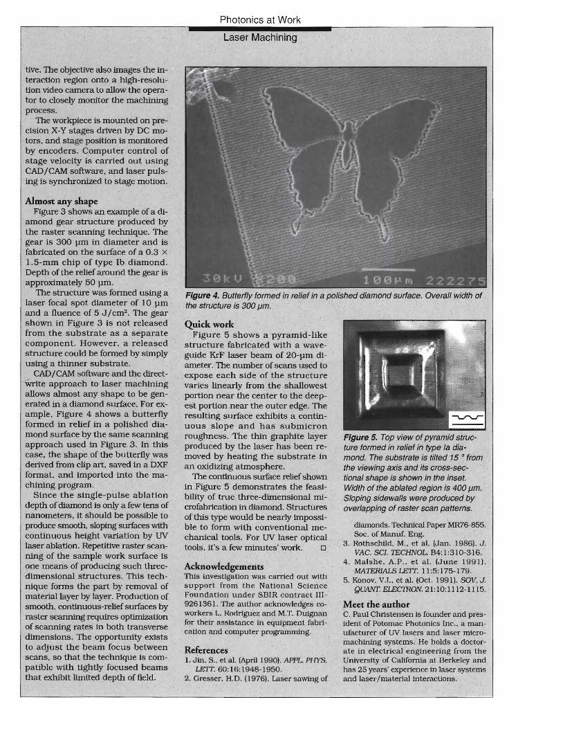
CAD/CAM software and the directWrite approach to laser machining allows almost any shape to be generated in a diamond surface. For example, Figure 4 shows a butterfly formed in relief in a polished diamond surface by the same scanning approach used in Figure 3. In this case, the shape of the butterfly was derived from clip art. saved in a DXF format, and imported into the machining program.
Since the single-pulse ablation depth of diamond is only a few tens of nanometers, it should be possible to produce smooth. sloping surfaces with continuous height variation by UV laser ablation. Repetitive raster scanning of the sample work surface is one means of producing such threedimensional structures. This technique forms the part by removal of material layer by layer. Production of smooth, continuous-relief surfaces by raster scanning requires optimization of scanning rates in both transverse dimensions. The opportunity exists to adjust the beam focus between
. scans, so that the technique is compatible with tightly focused beams that exhibit limited depth of field.
Laser Machining
Quick work Figure 5 shows a pyramid~like
structure fabricated with a wavegUide KrF laser beam of 20-pm diameter. The number of scans used to expose each side of the structure varies linearly from the shallowest portion near the center to the deepest portion near the outer edge. The resulting surface exhibits a continuous slope and has submicron roughness. The thin graphite layer produced by the laser has been removed by heating the substrate in an oxidizing atmosphere.
The continuous surface relief shown in Figure 5 demonstrates the feasibility of true three-dimensional microfabrication in 'diamond. Structures ofthis type woUld be nearly impossible to form with conventional mechanical tools. For UV laser optical tools. it's a few minutes' work. 0
Acknowledgements This investigation was carried out with support from the National Science Foundation under SBIR contract III9261361. The author acknowledges coworkers L. Rodriguez and M.T. Duignan for their assjstance In equipment f1;lbri
. cation and computer programmjng.
References 1. Jin. S .. et al. (April 1990). APPL PHYS.
LE1T. 60: 16: 1948-1950. 2 . Gresser. H.D. (1976). Laser sawing of
Figure 5. Top view of pyramid structure formed in relief in type la diamond. The substrate is tilted 15 0 from the viewing axis and its cross-sectional shape is shown in the inset. Width of the ablated region is 400 11m.
. Sloping sidewalls were produced by overlapping of raster scan patterns.
illamonds. Techriical Paper MR76-855. Soc. of Manuf. Eng. .
3. Rothschild. Moo et al. (Jan. 1986). J. VAC. SCI. 1ECHNOL B4:1 :310-316.
4. Malshe. A.P . . et al. (June 1991). MATERIALS LE1T. II :5: 175-179.
5. Konov. V.I .. et al. (Oct. 1991). SOV. J. QUANT. ELEC1RON. 21: 10: 1112-11 15. .
Meet the author C. Paul Christensen is founder and president of Potomac Photonics Inc .. a manufacturer of UV lasers and laser mjcromachining systems. He holds a doctorate in electrical engineering from the University of Califorrua at Berkeley and has 25 years' experience in laser systems and laser/material interactions.