firing series scrs at medium voltage - tom blair's …thomasblairpe.com/scrsfire.pdf · ·...
TRANSCRIPT

Firing Series SCRs at Medium Voltage: Understanding the Topologies Ensures the
Optimum Gate Drive Selection
Frank Peter Wahl III, Member, IEEE
Abstract-- After 40 years of evolution, the series Thyristor (SCR) stack remains the valve -of-choice for multi -megawatt applications such as solid-state transfer switches, motor soft starters, VAR compensators and high-energy physics. However, the SCR's enduring popularity resulted in an almost overwhelming number of gate-firing methods — at least ten widely used methods for medium voltage series stacks alone. To aid the engineer during the initial design or specification stage, a survey is made of the three fundamental series SCR gate drive topologies and their most common variants, including floating bias drivers, MV pulse transformers and light triggered designs. The advantages, limitations and inherent features of several methods are described and compared with the competing methods. Methods are also compared against established electrical requirements for gate triggering, discussed in the appendix, "Firing Series SCRs."
Index Terms-- firing card, gate drive, HVDC, high-voltage techniques, ignitron, light triggered, medium voltage, multilevel drives, SCR, static switch, thyristor.
I. INTRODUCTION
OR over one hundred years electrical engineers have controlled higher voltages through a cascade
of commonly available lower voltage rated components. One notable early example, described by Uhlmann [1], is a French dc transmission link using the "Thury" system, which used several dc generators in series to create 57 kVdc at power levels to 4 MW. From this early design, the field of applications for series-stacks has evolved to include solid-state "valve" designs for static transfer switches (STS) and protection circuits, multi-megawatt motor drives, high voltage dc (HVDC) transmission and pulsed power for high-energy physics experiments.
The viability of these systems depends on the proper coordination of the gate drive method and power device technology to meet the design requirements while observing cost constraints. This author has identified at least ten distinctly different medium voltage gate drive methods — all currently used in industry — each optimized to meet unique requirements related to the systems mentioned above.
For brevity, the scope of this discussion is limited to comparing the gate drive methods used for thyristors in line/load commutating and pulsed power supply designs controlling medium voltage. In this context, medium voltage is defined as line voltages on the order of 1kVac to 34 kVac and dc link voltages to 100 kVdc across a given stack assembly or "panel." The term high voltage in HVDC systems will refer to voltages from 100 kVdc to 600 kVdc.
According to Hingorani [2], typical HVDC systems have valve arrangements containing multiple "valve panels" each with up to 20 series thyristors. The differences in voltage potential within each panel are in the range considered medium voltage. Thus, the methods described here are applicable to the gate drive type used inside each panel. However, HVDC valve assemblies using multiple valve panels often use a hybrid of several bias methods discussed herein. The classification and comparison of these hybrid designs at the system level is outside the scope of this paper.
The popularity and diversity of stacked thyristor (a.k.a. silicon controlled rectifier, or SCR) designs is due in large part to their very favorable electrical characteristics, i.e., very low gate power requirements (typically <10 W average each), low on-state losses, and the availability of proven gate drive designs. To establish a baseline for comparing the various drive methods, an appendix, "Firing Series SCRs," briefly discusses the necessity for voltage ballasting and a "hard firing" gate profile, i.e., high open circuit voltage, high short circuit current, fast rise time, and a time -coherent leading edge.
F
This work was supported in part by research performed to meet rectifier upgrade requirements for the 60 MW Arc Jet Test Facility, NASA Ames Research Center, Moffett Field, CA. Frank Peter Wahl III is with Enerpro, Inc., Goleta, CA 93117 USA (e-mail: [email protected]).
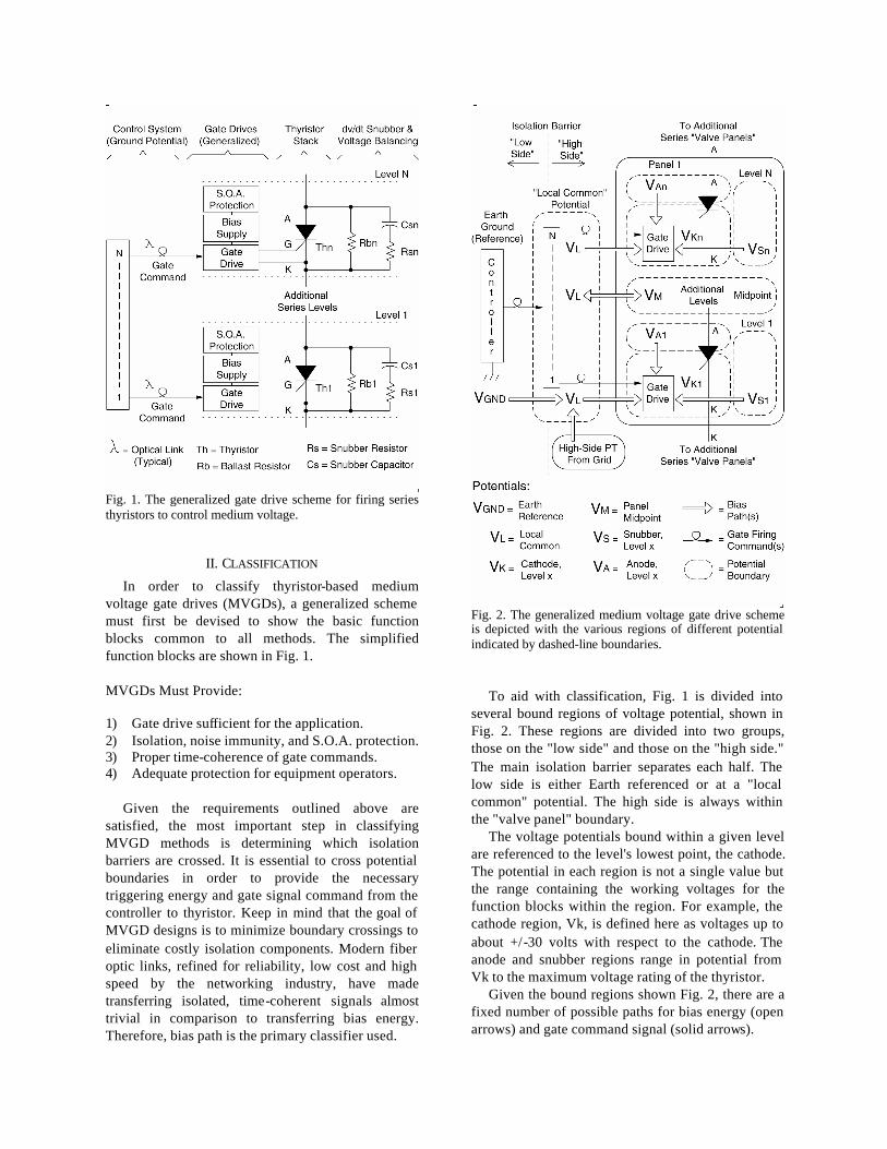
Fig. 1. The generalized gate drive scheme for firing series thyristors to control medium voltage.
II. CLASSIFICATION
In order to classify thyristor-based medium voltage gate drives (MVGDs), a generalized scheme must first be devised to show the basic function blocks common to all methods. The simplified function blocks are shown in Fig. 1. MVGDs Must Provide: 1) Gate drive sufficient for the application. 2) Isolation, noise immunity, and S.O.A. protection. 3) Proper time-coherence of gate commands. 4) Adequate protection for equipment operators.
Given the requirements outlined above are satisfied, the most important step in classifying MVGD methods is determining which isolation barriers are crossed. It is essential to cross potential boundaries in order to provide the necessary triggering energy and gate signal command from the controller to thyristor. Keep in mind that the goal of MVGD designs is to minimize boundary crossings to eliminate costly isolation components. Modern fiber optic links, refined for reliability, low cost and high speed by the networking industry, have made transferring isolated, time-coherent signals almost trivial in comparison to transferring bias energy. Therefore, bias path is the primary classifier used.
Fig. 2. The generalized medium voltage gate drive scheme is depicted with the various regions of different potential indicated by dashed-line boundaries.
To aid with classification, Fig. 1 is divided into
several bound regions of voltage potential, shown in Fig. 2. These regions are divided into two groups, those on the "low side" and those on the "high side." The main isolation barrier separates each half. The low side is either Earth referenced or at a "local common" potential. The high side is always within the "valve panel" boundary.
The voltage potentials bound within a given level are referenced to the level's lowest point, the cathode. The potential in each region is not a single value but the range containing the working voltages for the function blocks within the region. For example, the cathode region, Vk, is defined here as voltages up to about +/-30 volts with respect to the cathode. The anode and snubber regions range in potential from Vk to the maximum voltage rating of the thyristor.
Given the bound regions shown Fig. 2, there are a fixed number of possible paths for bias energy (open arrows) and gate command signal (solid arrows).
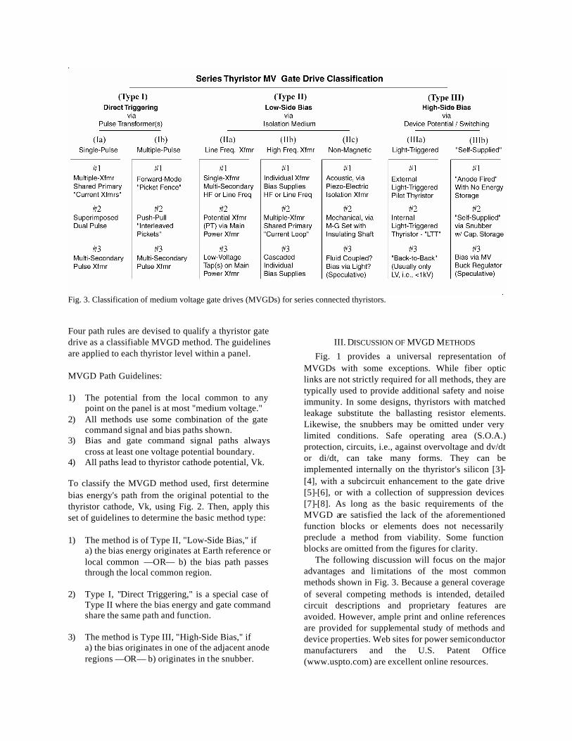
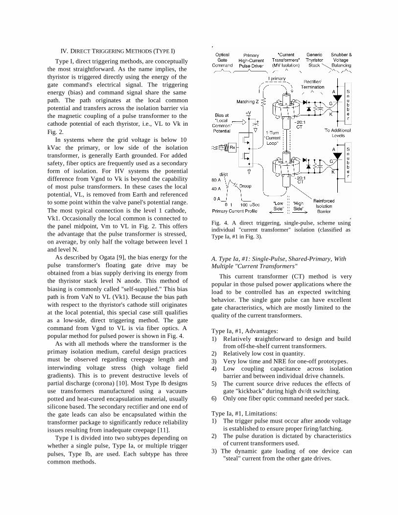
Fig. 3. Classification of medium voltage gate drives (MVGDs) for series connected thyristors. Four path rules are devised to qualify a thyristor gate drive as a classifiable MVGD method. The guidelines are applied to each thyristor level within a panel. MVGD Path Guidelines: 1) The potential from the local common to any
point on the panel is at most "medium voltage." 2) All methods use some combination of the gate
command signal and bias paths shown. 3) Bias and gate command signal paths always
cross at least one voltage potential boundary. 4) All paths lead to thyristor cathode potential, Vk. To classify the MVGD method used, first determine bias energy's path from the original potential to the thyristor cathode, Vk, using Fig. 2. Then, apply this set of guidelines to determine the basic method type: 1) The method is of Type II, "Low-Side Bias," if
a) the bias energy originates at Earth reference or local common —OR— b) the bias path passes through the local common region.
2) Type I, "Direct Triggering," is a special case of
Type II where the bias energy and gate command share the same path and function.
3) The method is Type III, "High-Side Bias," if
a) the bias originates in one of the adjacent anode regions —OR— b) originates in the snubber.
III. DISCUSSION OF MVGD METHODS
Fig. 1 provides a universal representation of MVGDs with some exceptions. While fiber optic links are not strictly required for all methods, they are typically used to provide additional safety and noise immunity. In some designs, thyristors with matched leakage substitute the ballasting resistor elements. Likewise, the snubbers may be omitted under very limited conditions. Safe operating area (S.O.A.) protection, circuits, i.e., against overvoltage and dv/dt or di/dt, can take many forms. They can be implemented internally on the thyristor's silicon [3]-[4], with a subcircuit enhancement to the gate drive [5]-[6], or with a collection of suppression devices [7]-[8]. As long as the basic requirements of the MVGD are satisfied the lack of the aforementioned function blocks or elements does not necessarily preclude a method from viability. Some function blocks are omitted from the figures for clarity.
The following discussion will focus on the major advantages and limitations of the most common methods shown in Fig. 3. Because a general coverage of several competing methods is intended, detailed circuit descriptions and proprietary features are avoided. However, ample print and online references are provided for supplemental study of methods and device properties. Web sites for power semiconductor manufacturers and the U.S. Patent Office (www.uspto.com) are excellent online resources.
IV. DIRECT TRIGGERING METHODS (TYPE I)
Type I, direct triggering methods, are conceptually the most straightforward. As the name implies, the thyristor is triggered directly using the energy of the gate command's electrical signal. The triggering energy (bias) and command signal share the same path. The path originates at the local common potential and transfers across the isolation barrier via the magnetic coupling of a pulse transformer to the cathode potential of each thyristor, i.e., VL to Vk in Fig. 2.
In systems where the grid voltage is below 10 kVac the primary, or low side of the isolation transformer, is generally Earth grounded. For added safety, fiber optics are frequently used as a secondary form of isolation. For HV systems the potential difference from Vgnd to Vk is beyond the capability of most pulse transformers. In these cases the local potential, VL, is removed from Earth and referenced to some point within the valve panel's potential range. The most typical connection is the level 1 cathode, Vk1. Occasionally the local common is connected to the panel midpoint, Vm to VL in Fig. 2. This offers the advantage that the pulse transformer is stressed, on average, by only half the voltage between level 1 and level N.
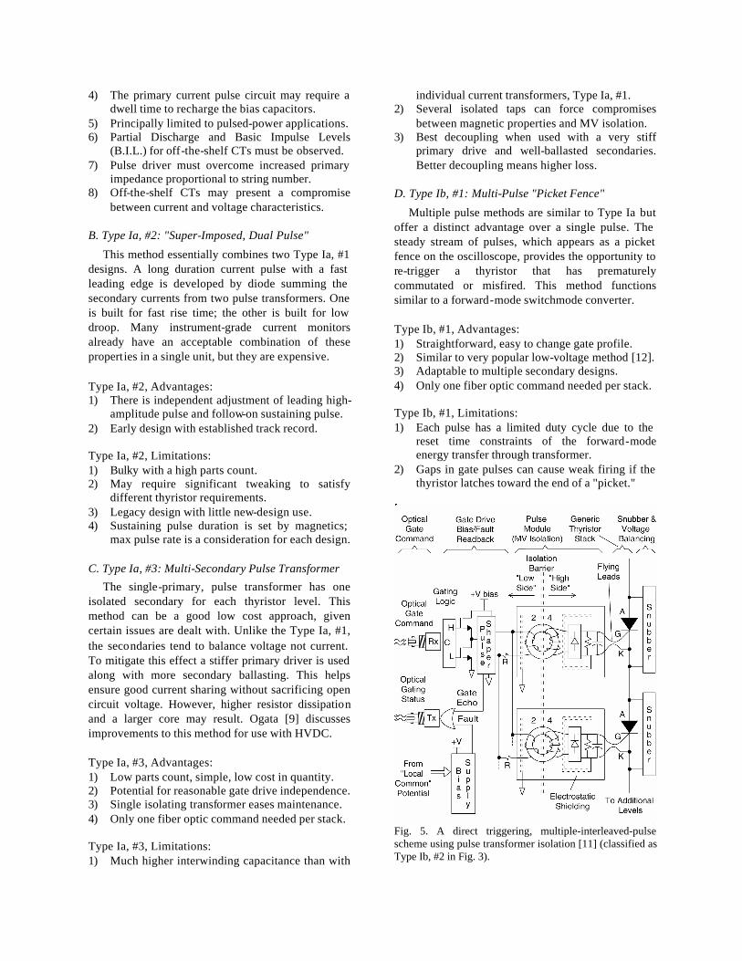
As described by Ogata [9], the bias energy for the pulse transformer's floating gate drive may be obtained from a bias supply deriving its energy from the thyristor stack level N anode. This method of biasing is commonly called "self-supplied." This bias path is from VaN to VL (Vk1). Because the bias path with respect to the thyristor's cathode still originates at the local potential, this special case still qualifies as a low-side, direct triggering method. The gate command from Vgnd to VL is via fiber optics. A popular method for pulsed power is shown in Fig. 4.
As with all methods where the transformer is the primary isolation medium, careful design practices must be observed regarding creepage length and interwinding voltage stress (high voltage field gradients). This is to prevent destructive levels of partial discharge (corona) [10]. Most Type Ib designs use transformers manufactured using a vacuum-potted and heat-cured encapsulation material, usually silicone based. The secondary rectifier and one end of the gate leads can also be encapsulated within the transformer package to significantly reduce reliability issues resulting from inadequate creepage [11].
Type I is divided into two subtypes depending on whether a single pulse, Type Ia, or multiple trigger pulses, Type Ib, are used. Each subtype has three common methods.
Fig. 4. A direct triggering, single-pulse, scheme using individual "current transformer" isolation (classified as Type Ia, #1 in Fig. 3).
A. Type Ia, #1: Single-Pulse, Shared-Primary, With Multiple "Current Transformers"
This current transformer (CT) method is very popular in those pulsed power applications where the load to be controlled has an expected switching behavior. The single gate pulse can have excellent gate characteristics, which are mostly limited to the quality of the current transformers. Type Ia, #1, Advantages: 1) Relatively straightforward to design and build
from off-the-shelf current transformers. 2) Relatively low cost in quantity. 3) Very low time and NRE for one-off prototypes. 4) Low coupling capacitance across isolation
barrier and between individual drive channels. 5) The current source drive reduces the effects of
gate "kickback" during high dv/dt switching. 6) Only one fiber optic command needed per stack. Type Ia, #1, Limitations: 1) The trigger pulse must occur after anode voltage
is established to ensure proper firing/latching. 2) The pulse duration is dictated by characteristics
of current transformers used. 3) The dynamic gate loading of one device can
"steal" current from the other gate drives.
4) The primary current pulse circuit may require a dwell time to recharge the bias capacitors.
5) Principally limited to pulsed-power applications. 6) Partial Discharge and Basic Impulse Levels
(B.I.L.) for off-the-shelf CTs must be observed. 7) Pulse driver must overcome increased primary
impedance proportional to string number. 8) Off-the-shelf CTs may present a compromise
between current and voltage characteristics.
B. Type Ia, #2: "Super-Imposed, Dual Pulse"
This method essentially combines two Type Ia, #1 designs. A long duration current pulse with a fast leading edge is developed by diode summing the secondary currents from two pulse transformers. One is built for fast rise time; the other is built for low droop. Many instrument-grade current monitors already have an acceptable combination of these properties in a single unit, but they are expensive. Type Ia, #2, Advantages: 1) There is independent adjustment of leading high-
amplitude pulse and follow-on sustaining pulse. 2) Early design with established track record. Type Ia, #2, Limitations: 1) Bulky with a high parts count. 2) May require significant tweaking to satisfy
different thyristor requirements. 3) Legacy design with little new-design use. 4) Sustaining pulse duration is set by magnetics;
max pulse rate is a consideration for each design.
C. Type Ia, #3: Multi-Secondary Pulse Transformer
The single-primary, pulse transformer has one isolated secondary for each thyristor level. This method can be a good low cost approach, given certain issues are dealt with. Unlike the Type Ia, #1, the secondaries tend to balance voltage not current. To mitigate this effect a stiffer primary driver is used along with more secondary ballasting. This helps ensure good current sharing without sacrificing open circuit voltage. However, higher resistor dissipation and a larger core may result. Ogata [9] discusses improvements to this method for use with HVDC.
Type Ia, #3, Advantages: 1) Low parts count, simple, low cost in quantity. 2) Potential for reasonable gate drive independence. 3) Single isolating transformer eases maintenance. 4) Only one fiber optic command needed per stack. Type Ia, #3, Limitations: 1) Much higher interwinding capacitance than with
individual current transformers, Type Ia, #1. 2) Several isolated taps can force compromises
between magnetic properties and MV isolation. 3) Best decoupling when used with a very stiff
primary drive and well-ballasted secondaries. Better decoupling means higher loss.
D. Type Ib, #1: Multi-Pulse "Picket Fence"
Multiple pulse methods are similar to Type Ia but offer a distinct advantage over a single pulse. The steady stream of pulses, which appears as a picket fence on the oscilloscope, provides the opportunity to re-trigger a thyristor that has prematurely commutated or misfired. This method functions similar to a forward-mode switchmode converter.
Type Ib, #1, Advantages: 1) Straightforward, easy to change gate profile. 2) Similar to very popular low-voltage method [12]. 3) Adaptable to multiple secondary designs. 4) Only one fiber optic command needed per stack. Type Ib, #1, Limitations: 1) Each pulse has a limited duty cycle due to the
reset time constraints of the forward-mode energy transfer through transformer.
2) Gaps in gate pulses can cause weak firing if the thyristor latches toward the end of a "picket."
Fig. 5. A direct triggering, multiple-interleaved-pulse scheme using pulse transformer isolation [11] (classified as Type Ib, #2 in Fig. 3).
E. Type Ib, #2: Multi-Pulse, Interleaved "DC Gating"
The Type Ib, #2 method, Fig. 5, is essentially a push-pull switchmode converter with virtually no output capacitance and a transformer capable of handling the first half-cycle switching event without saturation. The output's rectified square wave (dc) has an amplitude profile that is enhanced with a primary side pulse shaper to provide a strong leading edge [11].
The fiber optic receiver (Rx) converts the gate command light signal into the logic signal that is characterized by a square wave pulse train of approximately 200 pulses at a nominal frequency of 25 kHz and 5 msec duration (60 Hz line). The gating logic converts the signal into an even number of high-side and low-side pulses suitable for a totem-pole drive stage. The transformer is generally a high-permeability ferrite core of low turn count (1:2 ratio) to reduce parasitic inductance and interwinding capacitance. The bipolar square wave signal derived from the secondary is full-wave rectified via fast recovery rectifiers into a dc pulse. A terminating impedance of about 200 ohms and 0.01 uF can be used to enhance the noise immunity and help protect against transient gate reversal [13]. Type Ib, #2, Advantages: 1) Large amplitude, fast-rising edge possible. 2) Continuous interleaved sustaining pulses. 3) Very low interwinding capacitance push-pull
pulse modules. 4) Low corona signature pulse transformer feasible. 5) Adjacent gate drives are electrically independent. 6) The thyristor's gate structure remains in
saturation for the entire firing duration. This virtually eliminates misfires when compared to Type 1a, and Type Ib, #1.
7) Only one fiber optic command needed per stack. Type Ib, #2, Limitations: 1) May require a few milliseconds of dwell time to
establish optimum initial current profile. 2) The additional gating energy translates to more
low-side bias supply power required. 3) Proper design of the low-side transformer drive
circuit is essential for optimum magnetics utilization.
4) Some asynchronous, gated-oscillator designs may experience several microseconds of gate command latency.
5) Transformer reset must be ensured for optimum pulse amplitude/balance.
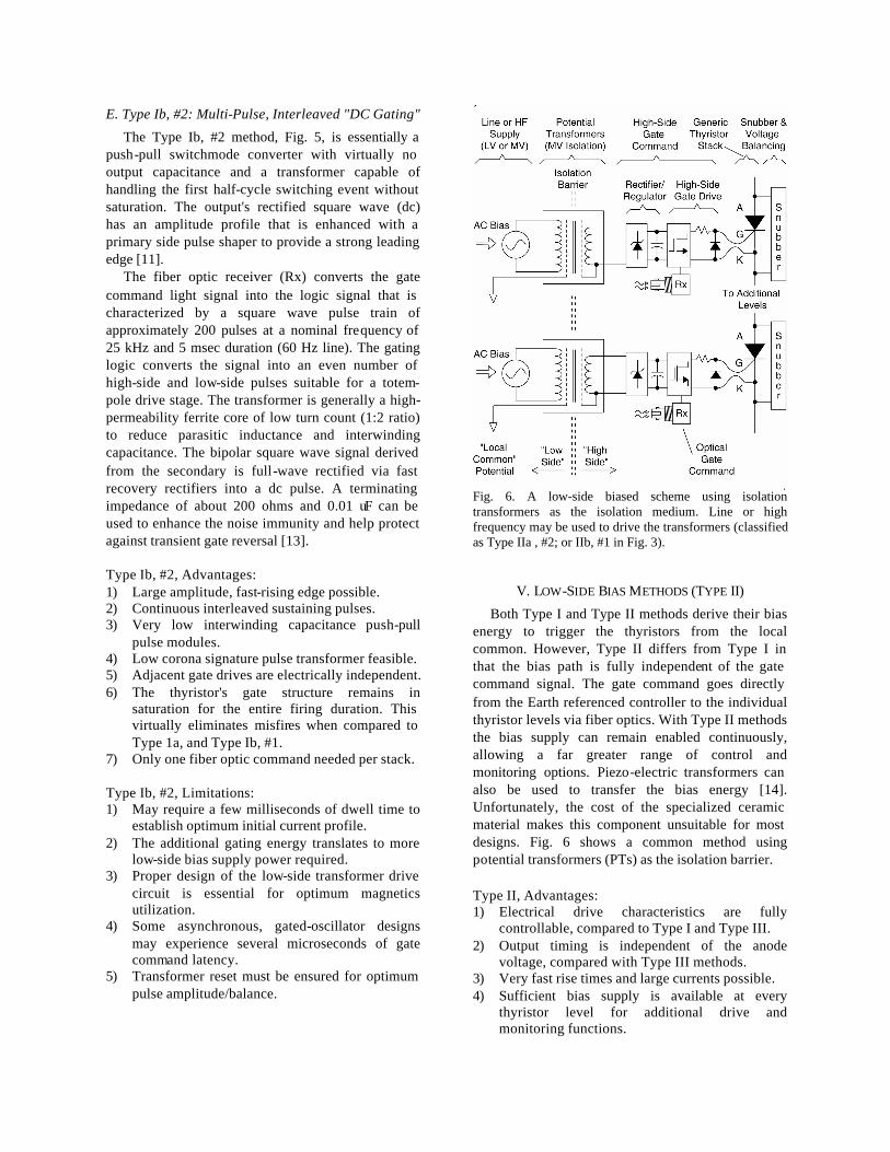
Fig. 6. A low-side biased scheme using isolation transformers as the isolation medium. Line or high frequency may be used to drive the transformers (classified as Type IIa , #2; or IIb, #1 in Fig. 3).
V. LOW-SIDE BIAS METHODS (TYPE II)
Both Type I and Type II methods derive their bias energy to trigger the thyristors from the local common. However, Type II differs from Type I in that the bias path is fully independent of the gate command signal. The gate command goes directly from the Earth referenced controller to the individual thyristor levels via fiber optics. With Type II methods the bias supply can remain enabled continuously, allowing a far greater range of control and monitoring options. Piezo-electric transformers can also be used to transfer the bias energy [14]. Unfortunately, the cost of the specialized ceramic material makes this component unsuitable for most designs. Fig. 6 shows a common method using potential transformers (PTs) as the isolation barrier.
Type II, Advantages: 1) Electrical drive characteristics are fully
controllable, compared to Type I and Type III. 2) Output timing is independent of the anode
voltage, compared with Type III methods. 3) Very fast rise times and large currents possible. 4) Sufficient bias supply is available at every
thyristor level for additional drive and monitoring functions.
5) Thyristor's gate structure remains in saturation for entire firing duration, virtually eliminating misfires compared to single-pulse methods.
Type II, Limitations: 1) The gate command signal's receiver, generally
involving fiber optics, is subject to a high voltage stress environment. Special precautions may apply regarding noise immunity and corona mitigation.
2) Each device in the string requires independent fiber optics and drive circuitry, high parts count, especially fiber optics, potentially compromising reliability.
3) Time coherence of command is dependent on the fiber optics (a minimal issue for modern optics).
F. Type IIa, #2; or IIb, #1: Individual, Line Frequency Transformers
This method is very straightforward and is a good choice for demonstrating a first-design prototype. The operation is evident by inspection of Fig. 6.
Type IIb, #1, Advantages: 1) Bias transformer may be fed directly from tap on
main power transformer. 2) The use of off-the-shelf potential transformers
(PTs) is possible, greatly simplifying the testing. 3) High gate-to-gate independence, easy to add
extra thyristor levels. Type IIb, #1, Limitations: 1) Line frequency transformers generally have high
interwinding capacitance and large size. 2) Systems for large numbers of devices may
become bulky. 3) Bias transformers may be more susceptible to
line sags than dc fed, low-side biasing schemes. 4) Requires one fiber optic command per thyristor.
G. Type IIa, #1: Multi-secondary Transformers
This method is identical in concept to Type IIb, #1 with the exception that the PT has multiple secondaries. Unwanted magnetic interactions are the only major drawback to this very simple method.
Type IIa, #1, Advantages: 1) Potentially smaller and less expensive than
individual transformers for large volume designs. Type IIa, #1, Limitations: 1) Transformer design is critical to achieve suitable
interwinding capacitance and isolation. 2) Less flexible than individual transformers
because the transformer is designed specifically
for a given number of thyristor levels. 3) Requires one fiber optic command per thyristor.
H. Type IIb, #1: Individual, High Frequency Transformers
This method uses a bias supply that is similar in design to the Type Ib, #2 driver and transformer. The difference is that the driver is continuously running and the gate command signal controls the secondary side of the pulse transformer. Almost all MV IGBT gate drives use this bias method. Type IIb, #1: Advantages: 1) Similar to existing MV IGBT drive designs and
thus relatively straightforward to understand. 2) Very modular in terms of expandability, and
reparability. 3) This method's push-pull transformer bias is
continuously running. The core can be much smaller than a Type Ib, #2 design because the core is allowed to saturate on startup.
Type IIb, #1: Limitations: 1) Higher parts count than designs that share the HF
transformer drive. 2) Requires one fiber optic command per thyristor.
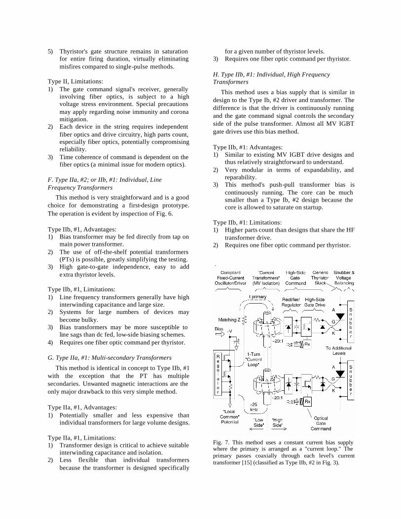
Fig. 7. This method uses a constant current bias supply where the primary is arranged as a "current loop." The primary passes coaxially through each level's current transformer [15] (classified as Type IIb, #2 in Fig. 3).
I. Type IIb, # 2: "Current loop" bias supply
This bias scheme combines the advantages of the Type IIb methods with the excellent dynamic properties of the coaxial primary transformer design. The only major drawback is that the coaxial interface isolation barrier is typically an air-immersed interface of high field stress. While several layers of insulation are used to ensure there is no arc over, the area is still subject to partial discharge. The cumulative effects of partial discharge are typically less of a concern for very low duty cycle, pulsed power applications where the anode potential is essentially an average dc value. A Type IIb, #2 method is described by Welleman [15] for use in pulsed power applications. Type IIb, # 2, Advantages: 1) Very common method used in industry. 2) Very modular, especially when the CTs are
aligned in a single, coaxial pass of primary wire. 3) Very low interwinding capacitance. 4) Short-term isolation and Basic Impulse Level
(B.I.L.) is very high for one-turn coaxially arranged CTs.
Type IIb, # 2, Limitations: 1) Usually exhibits some corona issues due to the
primary loop to secondary/transformer core air gap that is common to most designs of this type.
2) Current loop driver is a discrete, additional component that is sized per application, i.e., in proportion to number of thyristors in the string.
3) Requires one fiber optic command per thyristor.
J. Type IIb, #3: Cascaded HF transformers
This method is realized by creating an individual isolation transformer with an extra secondary. This secondary becomes the primary for the isolation transformer for the next higher level. This process continues until all levels are powered. Fig. 6 is will aid with visualization. The transformers are up-rated to handle the increased load. The transformer at level 1 has N loads; the Nth has a normal load. HF is used for the driver to minimize transformer size. Because isolation issues dominate the physical size of low VA potential transformers, the increase in VA may not increase physical size. The method's main advantage is that, on average, each isolation transformer is stressed by only 1/Nth the full blocking voltage.
Type IIb, #3, Advantages: 1) Potentially a very low corona method when a
significant amount of cascaded stages are used. 2) Potential for a very modular design.
Type IIb, #3, Limitations: 1) Bias supplies on the up-stream side may need to
be oversized to accommodate downstream load. 2) Interchangeability of drive modules dictates that
all modules are built to at least the largest bias supply requirement, i.e., each unit must be built as a master bias drive unit.
3) Upstream gate driver sections are under greater bias supply stress than downstream units.
4) Downstream loads (higher level number) are at the mercy of the upstream device's reliability.
5) Requires one fiber optic command per thyristor.
VI. HIGH-SIDE BIAS METHODS (TYPE III)
By definition, the bias energy for high-side methods originates and remains on the high side of the isolation barrier. Specifically, the bias originates from either the adjacent anode region(s) or the snubber region on the same level. Because no bias or signal paths depend on a local common as an origination or transit point, the local common exists arbitrarily. For sake of argument, the local common for a Type III MVGD is defined at the cathode potential (Vk in Fig. 2) for the gate drive of interest. Ideally, the largest potential experienced in normal operation is the breakdown voltage (or breakover voltage) of the thyristor — regardless of the stack length. This arbitrary assignment of local common implies that the panel voltage and/or the voltage with respect to Earth reference can be arbitrarily high. For practical considerations the stack length is still maintained at levels considered medium voltage.
Type III: High-Side Bias
Type III, Advantages: 1) No low-side bias required. 2) Gate command is via fiber. Complete galvanic,
electrostatic and magnetic isolation with respect to low-side gate signal (Earth reference).
3) Highest level of insulation and fault isolation. 4) Can be extremely compact and modular. Type III, Limitations: 1) Gating energy/power is generally limited due to
limitations in the energy recovery scheme 2) Gate drive performance is generally dependent
on delay angle, i.e., available anode voltage. 3) Limited high-side bias supply power available to
run diagnostic circuits. 4) Many MV "anode fired" circuits have a required
latency until the anode reaches the minimum required voltage.
5) Requires one fiber optic command per thyristor.
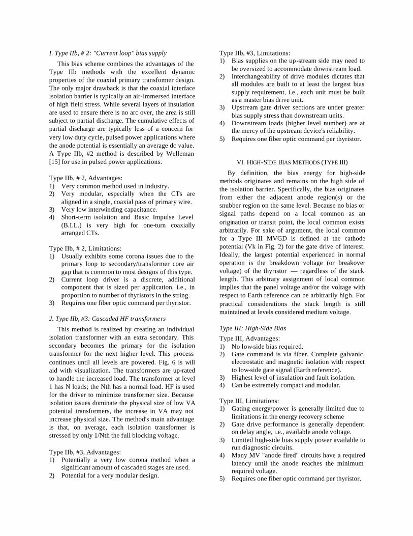
Fig. 8. A generalized external, light-activated pilot thyristor (ELTT) with external S.O.A. protection [3]-[16]-[19] (classified as Type IIIa, #1, in Fig. 3).
Type IIIa: Light-Triggered Thyristors
Light triggered thyristors (LTT) date back to the early 1960's, only about five years after the inception of electrically triggered power thyristors (ETT) [16]. Since then, LTTs have undergone continual improvements in both voltage ratings and in their ability to survive conditions of excessive di/dt [3], dv/dt [4], and overvoltage [6]-[7]-[17].
The LTT differs from an ETT in that light energy activates the initial sensitive amplifying gate structure rather than an externally supplied current. LTTs are classified as high-side bias method because essentially all of the actual triggering energy is derived from the anode (Fig. 8); otherwise they would qualify as direct triggering, Type Ia. According to Dorn [17], the required light power to trigger an LTT is about 40 mW for about 10 microseconds. The sensitivity of the gate is due to several stages of amplification. Several silicon-level enhancements have been made to the amplifying gate structure to improve the S.O.A. capability [3]-[4]-[17]. Otherwise, the LTT's power handling structure is similar to that of a conventional electrically triggered thyristor [17].
K. Type IIIa, #1: Externally Light-Triggered Thyristors (ELTT)
The ELTT method uses a separate package to
contain the light activated gate device, initial gate amplification stages, pilot SCR, and protection features [3]. This external light triggered pilot device is then connected to a conventional electrically triggered thyristor. Fig. 8 shows a generalized scheme. ELTTs are currently in use in static transfer switch installations [18]-[19]. Type IIIa, #1, Advantages: 1) Allows the use of "generic" thyristors. 2) Allows replacement of fiber and ELTT "pilot"
device without dismantling the stack. 3) Large installed user base [19]. Type IIIa, #1, Limitations: 1) Parts exposed to high voltage compared to
monolithically light triggered (LTT) devices. 2) Proprietary, ELTT has limited availability. 3) Shares same limitations as LTT.
L. Type IIIa, #2: Light Triggered Thyristors (LTT)
As described by Dorn [17] the LTT is a monolithic, light triggered device. The light signal enters through a windowed slot in the cathode pole face. A custom light carrying fiber cable assembly is preformed to fit into the pole face slot [22]. Fig. 9 shows the LTT's physical layout [17]. Applications include HVDC transmission systems, protection for HV capacitor banks [20], and pulsed power.
Type IIIa, #2, Advantages: 1) No exposed parts at HV, i.e., no driver board;
gate signal amplification is internal [17]. 2) Usually integrated with internal temp -tracking
B.O.D. and forward dv/dt protection. [17]. 3) Lowest corona signature. 4) Most compact, especially for pulsed power [21]. 5) Drive faults are contained within device housing. 6) The external electrical gate connections are
absent, improving reliability [17]. Type IIIa, #2, Limitations: 1) Dependent on anode voltage for gate drive. 2) Gating command (firing opportunities) supplied
in short pulses only, i.e., 10 microseconds. 3) Requires relatively expensive laser diode [22]. 4) B.O.D. is included usually by necessity. 5) Each thyristor requires its own fiber. Each stack
of N devices depends on N multiple fibers. 6) Optical power budget [22] dictates fiber length. 7) The special fiber cable may require an
experienced technician for splicing, termination. 8) High power laser diodes require special safety
precautions during commissioning [22]. 9) Proprietary thyristor and fiber link, expensive.

Fig. 9. A light-triggered thyristor scheme using an internal light-activated pilot thyristor (LTT) with built in S.O.A. Protection [17] (classified as Type IIIa, #2 in Fig. 3).
M. Type IIIb, #1, #3; Self-Supplied, "Anode Fired"
Type IIIb methods derive their energy from the anode of the thyristor being controlled. The fiber signal provides only the gating command signal and not the initial gating energy via light as the LTT and external LTT methods. Type IIIb methods are able to use relatively inexpensive and readily available fiber cables. However, conventional optical receivers are not designed to switch anode voltages. Some form of voltage regulator/limiter is used.
Few methods of anode firing without energy storage are currently in use. One method is "slave triggering." This legacy method uses the anode-switching transient of a "master" thyristor and capacitive level shifting to trigger the adjacent thyristor [26]. The string turns on in cascade. This method was not assigned a type because of its greatly limited use.
All present anode-fired methods require a "bootstrap" time to allow a sufficient precharge of the drive circuit bias. Some schemes may require a coordinated design between the snubber and the gate drives, given a specific application, in order to achieve an acceptable level of performance.
One method that may show promise for the future (speculative) is Type IIIb, #3. This method would use inexpensive switchmode buck regulators that could directly convert the multi-kilovolt anode potentials to levels suitable for a cathode-referenced gate drive.
Fig. 10. A high-side biased, self-supplied gate driver (SSGD) scheme using gating energy derived from the snubber [23]-[24] (classified as Type IIIb, #2 in Fig. 3).
N. Type IIIb, #2; Self-Supplied, With Capacitive Energy Storage
Self-supplied methods using an energy storage element generally derive the gating energy from the snubber's switching action. Two schemes are usually used to transfer the energy from high anode potential to cathode-referenced potentials reasonable for gate drive bias. Magnetic coupling of the snubber's switching current is one scheme used to recover bursts of energy during switching events. A more viable scheme uses capacitance [24] to recover charge via a capacitive divider. This scheme recovers charge over a much larger time period and works at a reduced capacity even when the thyristors are off. Most Type IIIb methods supplement the switching recovery scheme with a "bleeder" resistor to trickle charge the bias circuit when the thyristors are off.
A commercially viable [25], method of Type IIIb, #2 is described by Raonic [23]-[24]. This implementation, shown in Fig. 10, uses capacitive energy storage in addition to a capacitive divider energy recovery scheme with several improvements. The snubber current is actively diverted around the energy storage capacitor once it has achieved full charge [24]. This reduces regulator loss. The scheme uses an anode voltage feedback resistor to monitor the switching state and "economize the gating" [23].
Type IIIb, #2, Advantages: 1) A sufficient amount of gating energy is available
at a greater delay angle range when compared with anode firing alone.
2) Longer or multiple pulses per cycle are available (depending on delay angle). This allows the possibility for stronger triggering profiles.
3) A modest amount of bias for feedback available. Type IIIb, #2, Limitations: 1) A dwell time is needed to precharge the bias. 2) Bias charge will dissipate to zero when bypass
contactors are closed across the thyristor stacks. 3) The drive circuit may have finite dwell time
between when the bypass contactors open and the drive is active. During this short period, the thyristors may not be in control of the load.
4) Requires one fiber optic command per thyristor.
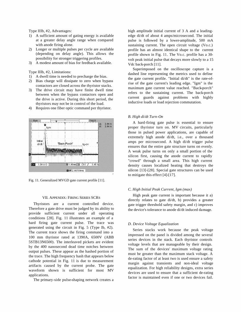
Fig. 11. Generalized MVGD gate current profile [11].
VII. APPENDIX: FIRING SERIES SCRS
Thyristors are a current controlled device. Therefore a gate drive must be judged by its ability to provide sufficient current under all operating conditions [28]. Fig. 11 illustrates an example of a hard firing gate current pulse. The trace was generated using the circuit in Fig. 5 (Type Ib, #2). The current trace shows the firing command into a 100 mm thyristor rated at 1390A, 6500V (ABB 5STB13N6500). The interleaved pickets are evident by the 400 nanosecond dead time notches between output pulses. These appear as the hashed portion of the trace. The high frequency hash that appears below cathode potential in Fig. 11 is due to measurement artifacts caused by the current probe. The gate waveform shown is sufficient for most MV applications.
The primary-side pulse-shaping network creates a
high amplitude initial current of 3 A and a leading-edge di/dt of about 4 amps/microsecond. The initial pulse is followed by a lower-amplitude, 500 mA sustaining current. The open circuit voltage (Vo.c.) profile has an almost identical shape to the current profile shown in Fig. 11. The Vo.c. profile has a 30-volt peak initial pulse that decays more slowly to a 15 Vdc back-porch [11].
Superimposed on the oscilloscope capture is a dashed line representing the metrics used to define the gate current profile. "Initial di/dt" is the rate-of-rise of the gate current's leading edge. "Igm" is the maximum gate current value reached. "Back-porch" refers to the sustaining current. The back-porch current guards against problems with highly inductive loads or load rejection commutation.
B. High di/dt Turn-On
A hard-firing gate pulse is essential to ensure proper thyristor turn on. MV circuits, particularly those in pulsed power applications, are capable of extremely high anode di/dt, i.e., over a thousand amps per microsecond. A high di/dt trigger pulse ensures that the entire gate structure turns on evenly. A weak pulse turns on only a small portion of the silicon first, causing the anode current to rapidly "crowd" through a small area. This high current density causes localized heating that destroys the silicon [13]-[28]. Special gate structures can be used to mitigate this effect [4]-[17].
C. High Initial Peak Current, Igm (max)
High peak gate current is important because it a) directly relates to gate di/dt, b) provides a greater gate trigger threshold safety margin, and c) improves the device's tolerance to anode di/dt induced damage.
D. Device Voltage Equalization
Series stacks work because the peak voltage impressed on the panel is divided among the several series devices in the stack. Each thyristor controls voltage levels that are manageable by their design. The sum of the devices' maximum voltage rating must be greater than the maximum stack voltage. A de-rating factor of at least two is used ensure a safety margin against transients and non-ideal voltage equalization. For high reliability designs, extra series devices are used to ensure that a sufficient de-rating factor is maintained even if one or two devices fail.
One of the worst things that can happen to a stack is a cascading overvoltage failure. This originates when one device fails from overvoltage. Because thyristors fail to short-circuit, the stack voltage is then impressed across the remaining devices. If the remaining devices cannot block the voltage, then they also will fail, one by one, at an increasing rate.
Voltage equalization is important during static conditions (thyristor off) and dynamic (switching) conditions. Dynamic voltage equalization [1]-[13]-[26] is beyond the scope of this paper.
Ballasting resistors, which function as a voltage divider network, are the most common way to accomplish static voltage balance. Ballasting ensures that differences in the device leakage currents and other parasitic paths are swamped out by the current in the ballast resistor path. Some MVGD methods, particularly Type III, use forced equalization circuits to either shunt the transient [7]-[8], or safely trigger the thyristor during overvoltage events [4]-[5]-[7]-[8]. Methods that use this "emergency-triggering" scheme usually have an extra number of thyristor levels to prevent an unintended cascade firing of additional thyristors. Cascading, emergency triggering events even of the entire string will not necessarily damage the devices, but the event is usually not good for the rest of the system.
Voltage equalization is a fundamental requirement for all medium voltage stacks. Careful consideration of this factor is an important step when designing or specifying either series stacks or MVGD methods. The topic of string voltage equalization is covered in depth by several sources [1]-[7]-[8]-[26].
E. Time Coherence of Pulse Leading Edges
Time coherence is important to ensure good dynamic voltage equalization. If one gate significantly leads the others, then one thyristor will turn on early. This forces the other devices to pick up the slack. The dv/dt limiting of the snubber [26] will help but not cure this problem. Ideally all gate pulses will occur at virtually the same time. The Type Ib, #2 method described by Wahl [11] has a leading-edge time coherence of better than about 100 nanoseconds. The time difference was measured at a one-amp level on the outputs of a six-device MVGD.
VIII. CONCLUSION
This objective of this paper is to provide an overview of several popular topologies used to trigger thyristors controlling medium voltage. The general structure of the MV gate drive is explained in order to develop a methodology for classifying the
major design types. Special emphasis was placed on providing the practical advantages, disadvantages and design features affecting decisions at the specification stage. The author has verified via online research and the references listed, that each method mentioned is commercially viable and currently in use by industry. Company names were intentionally not mentioned. (They are available upon request.) Instead, generalized circuits are described, with proprietary information referenced by its patent source. The information presented here will help significantly during the initial design and specification stage, but is not intended as a stand-alone MVGD design guide. Most all power thyristor manufacturers cover thyristor gate characteristics in great detail. The reader is encouraged to study this subject and the references included before embarking on a MVGD design.
IX. ACKNOWLEDGMENT
The author gratefully acknowledges the contributions of Frank J. Bourbeau and the late John E. Mungenast for their assistance and support toward this document.
X. REFERENCES [1] E. Uhlmann, Power Transmission by Direct
Current, New Springer-Verlag, New York, 1975, (ISBN: 0-387-07122-9).
[2] N. G. Hingorani, "The Rise of High-Voltage, Direct Current Systems," IEEE Spectrum, April 1996. [Online]. Available: http://www.spectrum.ieee. org/publicaccess/9604teaser/9604pow1.html.
[3] V. A. K. Temple, “Controlled Turn-On Thyristor,” U.S. Patent 4 908 687, Mar. 13, 1990.
[4] M. Ruff, H.-J. Schulze, F. Pfirsch, "Thyristor with Integrated dU/dt Protection," U.S. Patent 6 066 864, May 23, 2000.
[5] "Breakover Diodes," Application Note H-6, IXYS Corporation, 2000. [Online]. Available: http://www.ixys.com/pfbods01.html.
[6] H. Lawatsch and J. Vitins, "Protection of Thyristors Against Overvoltage with BOD Break-Over Diodes," proc. 1985 IEEE Ind. Applicat. Society, pp. 935-939.
[7] "Protection of Semiconductors with Symmetrical Silicon Surge Voltage Suppressors," Application Note No. 5SYA2011-01, ABB Semiconductors AG, Jan. 1999.
[8] P. Chadwick, "Thyristor-Switched Capacitor Apparatus," U.S. Patent 4 475 139, Oct. 2, 1984.

[9] F. Ogata, “High-Voltage Thyristor Converter,” U.S. Patent 4 084 221, Apr. 11, 1978.
[10] G. J. Paoletti and A. Golubev, "Partial Discharge Theory and Technologies Related to Medium-Voltage Electrical Equipment," IEEE Trans. Ind. Applicat., Vol. 37, No. 1, pp. 90-103, Jan./Feb. 2001.
[11] F. P. Wahl III "The MVTB Family of Fiber-Optically Coupled Medium Voltage Thyristor Trigger Boards," Product Datasheet PD744, Enerpro Inc., July 2002. [Online]. Available: http://www.enerpro-inc.com.
[12] 1999 Semikron Power Electronics Data Book , Semikron International GmbH & Co.KG, Neurnberg, Germany, Aug. 1998, pp. A-104 A-108.
[13] L. R. Rice, Silicon Controlled Rectifier Designer's Handbook, Westinghouse Electric Corporation, (2nd Ed.), Sept. 1970.
[14] J. Williams, "An Acoustic Transformer Powered Super-High Isolation Amplifier," Application Note AN-285, National Semiconductor Corp., Oct. 1981. [Online]. Available: http://www.national.com.
[15] A. Welleman, E. Ramezani, U. Schlapbach, “Semiconductor Switches Replace Thyratrons & Ignitrons,” ABB Semiconductors AG, Lenzburg, Switzerland, June 2001.
[16] D. R. Grafham and E. K. Howell, "The Light Activated Switch," App. Note 200.29, General Electric Company, Auburn, NY, Feb. 1963.
[17] J. Dorn, U. Kellner, F.-J. Niedernostheide, H.-J. Schulze, "State of the Art Light Triggered Thyristors with Integrated Protection Functions," eupec GmbH, 2000. [Online]. Available: http://www.eupec.com.
[18] W. Spencer, “Static Transfer Switch: Ideal Solution Across a Spectrum of Applications” Silicon Power Corporation, Exton PA, [Reprint]. Power Quality Magazine, April 2000.
[19] "Medium Voltage PowerDigm," Product Brochure, Silicon Power Corporation, Exton, PA, [Online]. Available: http://www.siliconpower.com.
[20] "Light-Fired Thyristors Protect Capacitor Banks," Power Electronics Europe, Issue 5, 2000, pg. 54.
[21] H. G. Wisken, F. Podeyn, T. H.G.G. Weise, TZN-Research and Development, Unterluess GmbH; J. Dorn, D. Westerholt, eupec GmbH, "Light Activated Semiconductors for ETC Pulsed Power Applications," Germany.
[22] Information on the LTT light pipe (LIR 200 AH) and laser diode (SPL PL90) is available from Prinz Optics, Stromberg, Germany. [Online]. Available: http://www.prinzoptics.de.
[23] D. M. Raonic, "SCR Self-Supplied Gate Driver for Medium Voltage Application with Capacitor as
Storage Element," IEEE Trans. Ind. Applicat., Vol. 36, No. 1, pp. 212-216, Jan./Feb. 2000.
[24] D. Raonic, D. S. MacLennan, D. G. Rouaud, "Self-Powered Gate Driver Board," U.S. Patent 5 796 599, Aug. 18, 1998.
[25] "MV Dialog Plus OEM Kits," Product Brochure 1503D, (1500-1.0-jun97.pdf), Rockwell Automation, Medium Voltage Business, Cambridge, ON, Canada, June, 1997, pg. 18. [Online]. Available: http://www.ab.com/mvb.
[26] D. R. Grafham and J. C. Hey, General Electric SCR Manual Including Triacs and Other Thyristors, (5th ed.), General Electric Company, Syracuse, NY, 1972.
[27] "Gate Triggering and Gate Characteristics," Application Note, AN4840, Dynex Semiconductor Ltd., Jan. 2000. [Online]. Available: http://www.dynexsemi.com.
[28] "PCT Data Book -- Application Aspects, Section 5," ABB Semiconductors AG, Lenzburg, Switzerland, 2002, pp. S5-1, S5-5, [Online]. Available: http://www.abb.com/semicomductors.
[29] Powerex Rectifier and Thyristor Applications and Technical Data Book, (1st ed.), Powerex, Incorporated, Youngwood, PA, pp. 14-24, Aug. 1993. [Online]. Available: http://www.pwrx.com.
Frank Peter Wahl III (B'96) Graduated from California Polytechnic State University, San Luis Obispo, where he received a B.Sc. Degree in Electrical Engineering. During this period he donated considerable time to designing educational displays for National Engineering Week and
implementing electro-hydraulic animation systems for the Pasadena Tournament of Roses Parade. His employment experience includes multiple-kilowatt IGBT arc lamp ballasts for JVI Corp., San Luis Obispo, CA, graphically based test systems for National Semiconductor's Power Management Group, Santa Clara, CA, and technical and managing editor responsibilities for PCIM Power Electronic Systems magazine, Ventura, CA, from 1997 to 1999. He is currently a design engineer with Enerpro, Incorporated, Goleta, CA. His work includes mixed-signal controllers, line-commutated thyristor gate firing cards, and medium voltage thyristor-based power systems. He is a member of IEEE.