first paper in 1984 on fadcs fadc cost power ram power ecl ttl narrow & deep need: wide &...
TRANSCRIPT

First Paper in 1984 on FADCS
FADCCostCost Cost
Power
RAMPower ECL TTLNarrow & Deep
Need: Wide & ShallowMore Expensive then FADC
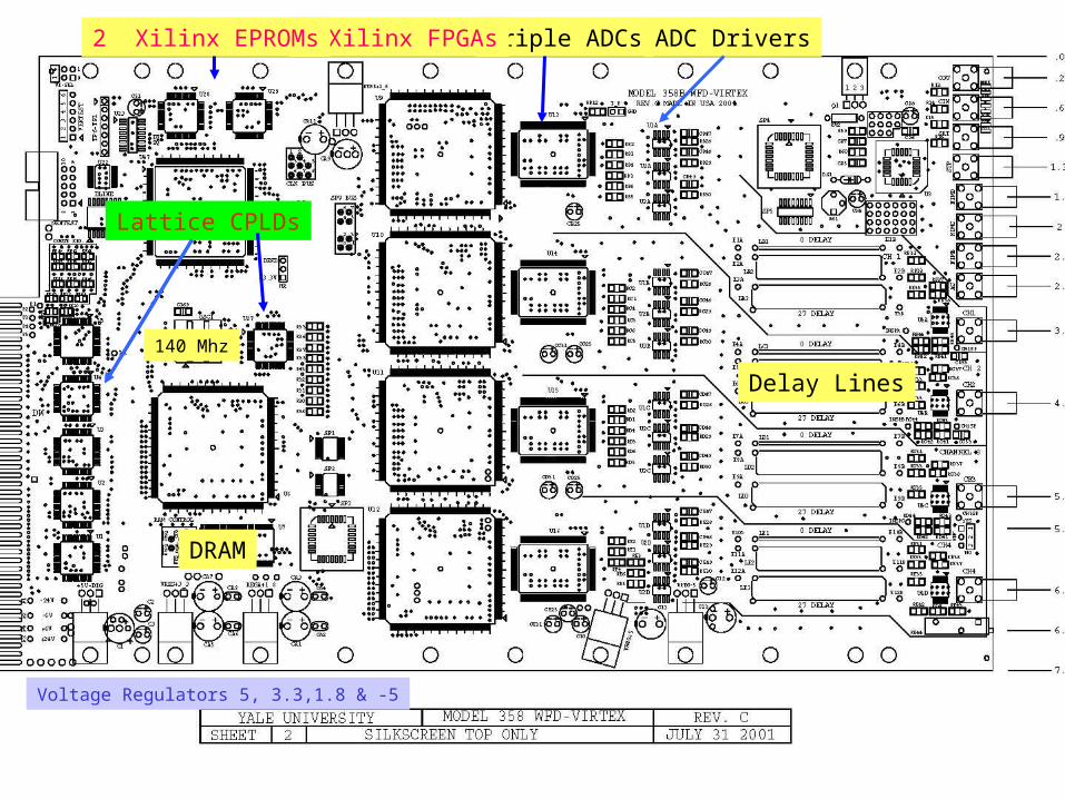
Triple ADCs5 Xilinx FPGAs
Lattice CPLDs
2 Xilinx EPROMs
DRAM
Delay Lines
Analog SectionInfrastructure
ADC Drivers
140 Mhz
Voltage Regulators 5, 3.3,1.8 & -5

Analog Front End
Delay Lines
Delay Lines Buried in PCB

> 240 Channels are being used at BNL & PSI
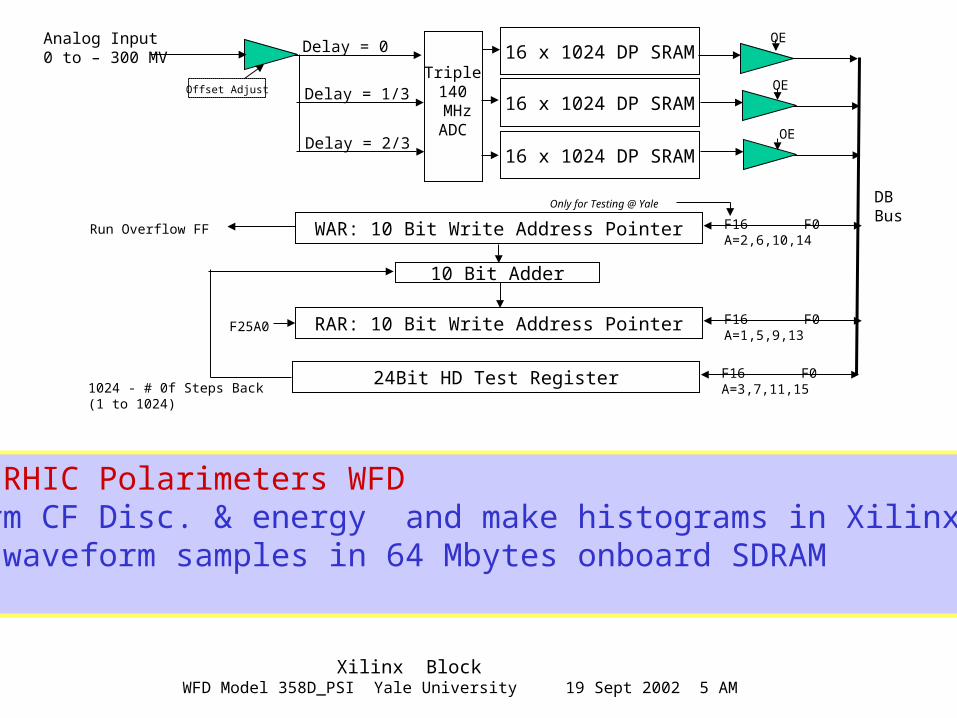
Analog Input0 to – 300 MV
Delay = 2/3OE
Delay = 1/3OE
16 x 1024 DP SRAM Delay = 0OE
WAR: 10 Bit Write Address Pointer F16 F0A=2,6,10,14
RAR: 10 Bit Write Address Pointer F16 F0A=1,5,9,13
10 Bit Adder
24Bit HD Test Register F16 F0A=3,7,11,151024 - # 0f Steps Back (1 to 1024)
DB Bus
F25A0
Run Overflow FF
Xilinx BlockWFD Model 358D_PSI Yale University 19 Sept 2002 5 AM
Only for Testing @ Yale
16 x 1024 DP SRAM
16 x 1024 DP SRAM
Triple140
MHzADC
Offset Adjust
AGS & RHIC Polarimeters WFDPerform CF Disc. & energy and make histograms in Xilinx ChipWrite waveform samples in 64 Mbytes onboard SDRAM

TTL Clk Out
NIM D
AC Clk In
Yes
NO
Model 358D- 200E
0 to 0.5 V
DC Input Offset AdjustClockwise More Positive
NIM C
Ch 1 Input
Ch 2 Input
Ch 4 Input
Ch 3 Input
Select DC Reference
NIM
Inputs Only
50 Ohm
Input Range
+/- 0.5 Vpp
Front Panel
NIM B
NIM-TTL10H125
OR
Pin 1 140 MHz XTL Pin 3
171 - SPCLK3 - 12
170 – SPCLK4 - 13
79 – MCCLKEN- 40 CLK_ENB
169 – SPCLK5 - 14EXT__IN
T
Stop TriggerARM II Out 14 Sec
187 – CamCLK- 10
168 – SPCLK6 - 15
8 - GCKO–92 Virtex
Load HD Register
ADC Encode Clock Fanout
SR8.ar
ADC Run
Yale University
Top Level Schematic
Model 358D_200E 14 Jan 2003 4:00 PM
172 – SPCLK2 - 11Read Clk - XMHZ
ARM I OutRead Clock XMHZ Out
External 140 MHz
ADC Clock Out
SR4.ar
Xilinx JTAG
Lattice JTAG
JTAG
Back Panel
EPROM
Xilinx Load Mode
0GG 1
1 XMHZ
2 YMHZ
3 AA0
4 AA1
5 Prog
6 Done
7 Gnd
Test Points
Stop Trigger
193 – !CamCLK- 9
8
To GCKO of Virtex Chips
SR CamCTL
Bit Signal Names PCB Line Pin #
0 Osc_Enb
1 Clk_Enb
2 Clk: Ext_ Internal. Int = 0
3 Disable Ram Addr Incr
4 Wait for Ext Trig
5 DONE
6 AA3 Run OverFlow Input
7 AB3 Run OverFlow Input
8 Write Port WEA: SPV0 SPV0 92
9 Write Port ENA: SPV1 SPV1 91
10 Write Port RSTA: SPV2 SPV2 90
11 Read Port WEB: SPV3 SPV3 89
12 Read Port ENB: SPV4 SPV4 93
13 Read Port RSTB: SPV5 SPV5 96
14 F9*A1*S1 # Sys_Rst SPV6 97
15 AC3 Run OverFlow Input SPV7 98
ADC_Mux_Clr 78
16 AD3 Run OverFlow Input
17 0
Comments
S1 HD0 136 67
S2 HD1 137 68 Not Used
F0 HD2 138 70 Not Used
F2 HD3 139 71
F16 HD4 140 72
F17 HD5 141 73 Not Used
BA1 HD6 142 74
BA2 HD7 143 78
1Volt PP Sinewaves
TTL C TTL B TTL A

Parts List M358B
Qty For
Qty/ Unit Cost Per 25 Extended
# PCB Description Manf. Part # Order # Price Board Boards InventoryNeeded Order qty Price
1 5 FPGA Xilinx XCV200E- 6 PQ240CINS 103002 76.55$ 382.75$ 125 0 125 115 8,803.25$ 2 2 jtagPROM Xilinx XC18V04VQ44C INS 103002 26.60$ 53$ 50 10 40 40 1,064.00$ 3 4 ADC ADI AD9483KS-140 FAI 092702 27.00$ 108$ 100 11 89 80 2,160.00$ 4 12 Diff Amp ADI AD8131AR FAI 092702 2.69$ 32$ 300 30 270 250 672.50$ 5 4 Driver Amp TI THS6022CPWP INS 103002 3.59$ 14$ 100 16 84 75 269.25$
6 1 DRAM Micron MT48LC16M16A2TG-75AV 072301 7.15$ 7$ 25 0 25 25 178.75$ 7 1 CamCTL Lattice M4A3-256/160-10YC-12YIAV 072301 20.90$ 21$ 25 6 19 24 501.60$ 8 5 Dataway Drv Lattice M4A5-64/32-10VC AV 072301 3.65$ 18$ 125 45 80 100 225.00$ 9 1 Clock Driver Lattice M4A3-32/32-5VC AV 072301 2.25$ 2$ 25 2 23 25 56.25$ 10 1 Oscillator 140 MHz Fox JITO-2-PC3AE-140 Quick Order 4.54$ 5$ 25 12 13 25 113.50$ 11 1 MM74H423AM Fairchild/Phil PHISN74HC123D FAI 0.19$ 0$ 25 100 -75 0 -$ 12 1 74 LCX 244T ST/Fairchild FSCSN74 LCX 244DGGFAI052201 0.22$ 0$ 25 100 -75 0 -$ 13 1 MECL-TTL Motorola MC10H125FN FAI 092702 2.49$ 2$ 25 9 16 20 49.80$ 14 2 Ferrite SMT 1806 6A 60 Ohms HI 1806T600R DK072301 0.26$ 0.510$ 50 200 -150 0 -$ 15 8 Diodes Case LL34 592-RLS4154 or RLS92 MS072301 0.046$ 0.368$ 200 137 63 100 4.60$
16 2 Fuse 3Amps LF251003 FAI 051401 0.18$ 0$ 50 60 -10 0 -$ 17 2 1.8 V Regulator 1.5A ST LD1086V18 Mouser:511-LD1086V18 2.00$ 4$ 50 135 -85 0 -$ 18 1 3.3 V Regulator 1.5A ST LD1086V33 Mouser:511-LD1086V33 0.96$ 0$ 25 20 5 25 5.75$ 19 2 5 V Regulator 3.0A Micrel MIC29300-5.0BT FAI 092702 2.49$ 5$ 50 40 10 15 37.35$ 20 1 . -5 V Regulator 1.0A NSC LM2990T-5.0 2.00$ 2$ 25 52 -27 0 -$ 21 1 2N5195 PNP 2N5195 FAI 051401 0.40$ 0$ 25 100 -75 0 -$ 22 1 1N4008 Diode 0.10$ 0$ 25 40 -15 0 -$ 23 12 LEMO Right Angle LemoUSA 6.00$ 72$ 300 46 254 300 1,800.00$ 24 1 JTAG Lattice Connector Digikey:MHD10K-ND 1.00$ 1$ 25 8 17 15 15.00$ 25 1 JTAG Xilinx Connector Newark 1.00$ 1$ 25 46 -21 -$ 26 1 Offset Connector Mouser: 571-1033611 0.50$ 1$ 25 26 -1 0 -$ 27 6 LED FAI 051401 0.13$ 1$ 150 54 96 110 13.75$ 28 1 PC Board 59.00$ 59$ 25 0 25 0 -$ 29 1 Assembly 150.00$ 150$ 25 25 0 -$ 30 1 Front Panel 30.00$ 30$ 25 0 5 31 2 Rails Techni Fab P3208 4.25$ 9$ 50 50 50 212.50$ 32 220 .1 uF 1206 Xicom Mouser: 140-CC502Z104M 0.026$ 5.720$ 5500 6000 -500 0 -$ 33 4 .1 uF .1inch 0.05$ 0.200$ 100 13 87 0 -$ 34 1 4.7uF 35V .1inch 0.22$ 0.220$ 25 200 -175 0 -$ 35 20 15uF 10V .1inch 0.22$ 4.400$ 500 264 236 500 110.00$ 36 4 68uF 10V .1inch 0.45$ 1.800$ 100 50 50 100 45.00$ 37 1 10Turn 50K Pot 3006P Bourns 3006P-503-ND DK072301 1.58$ 1.575$ 25 6 19 10 15.75$ 38 1 1Turn 500 Pot 3329P Bourns 1.00$ 1.000$ 25 0 25 30 30.00$ 39 1 TPStrip - 7 Female Berg 0.40$ 0.400$ 25 -$ 40 1 Misc SMD Components 25.00$ 25.000$ 25 -$
Total = 1,022.593$ 16,384$
13-Dec-02
10:00 AM

1.4 W


4 More
Lemos
ADCs Diff in / Diff Out
WFD Model 361 : 8 Channel 10 bits @ 250 MHz
Unchanged except for Clock

1. RHIC Polarimeters 10 Mbytes/ sec for 4 Channel Module2. Parallel bus systems can’t handle the rates3. Look at serial systems4. VITA34 Card size 8Ux220 mm Document in Draft Stage5. Time Scale >2 year. R. Downing ( FASTBUS & VME for Physics)
6. ATCA (Advanced Telecom Computing Architecture)7. 8Ux280 mm 140 sq inch -48V Power8. Switch Fabric: Mesh /Star/ Dual Star9. Star: Each slot had 4x connection to the 2 Controller slots10. Mesh: Peer – Peer connection11. Xilinx: Yale has PCI Express IP Core & Demo Unit
Current work

What is Next ?
• Need Larger PCB Size• Mucho amounts of current @ 1.2 Volts and Lower• Use Commodity Parts / Standards• Serial Interconnect• Very High Data Transmission on Copper• Infiniband Standard: Clocking @ 2.5 GHz• Embedded Clocking• Cables 10 to 20 Meters

1x LaneConsists of 2 Twisted pairs
20 inches on FR4 – 4 Layer PCB
Next is x2 Higher
250 Mbytes/sec
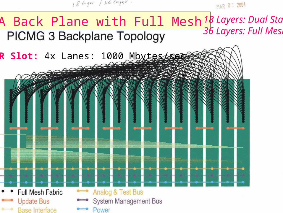
ATCA Back Plane with Full Mesh 18 Layers: Dual Star36 Layers: Full Mesh
PER Slot: 4x Lanes: 1000 Mbytes/sec

• Move Data Faster from the Front End to Computer Memory
• Embed PCI Express Silicon on Front End
• Copper Connections to @ 5 GHz and then11 GHz
• PCI Express Base (Need 1x) and not Infiniband (4x)
• Advanced Switching for Routing Event Data
• Trigger Processing Dual CPU sharing Memory
• Year 2006 Memory will be serial 32 Giga Bytes /sec
Data Moving in Future !

STT-SLT
Gigabit Ethernet Switch*
GTT Farm*
12 Dual 1 GHZ PCs
Event Builder Interface PC
GSLTInterface PC
8 TP Links
2 TP – PCI Cards
Preprocessor 1 PC
ProposedAdditions
Current VME Crate
CTD-SLT
8 TP LinksMVD ADC Crates
4 TP – PCI Cards
Preprocessor 1 PC
VME Crate VME Crate VME Crate VME Crate
Preprocessor 1 PC
Preprocessor 1 PC
Preprocessor 1 PC
Fast Ethernet
Fig. 4 ZEUS Global Track Trigger (GTT)
* Intel Grant Equipment
Run Control*Quad 700MHzPC
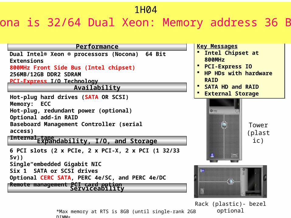
Performance
Availability
Expandability, I/O, and Storage
Serviceability
6 PCI slots (2 x PCIe, 2 x PCI-X, 2 x PCI (1 32/33 5v))Single embedded Gigabit NICSix 1” SATA or SCSI drives Optional CERC SATA, PERC 4e/SC, and PERC 4e/DCRemote management PCI card option
Hot-plug hard drives (SATA OR SCSI)Memory: ECCHot-plug, redundant power (optional)Optional add-in RAIDBaseboard Management Controller (serial access)Internal tape
Dual Intel® Xeon ® processors (Nocona) 64 Bit Extensions800MHz Front Side Bus (Intel chipset)256MB/12GB DDR2 SDRAM PCI-Express I/O Technology
Rack (plastic)- bezel optional
Tower(plastic)
Key Messages Intel Chipset at 800MHz PCI-Express IO HP HDs with hardware RAID SATA HD and RAID External Storage
Key Messages Intel Chipset at 800MHz PCI-Express IO HP HDs with hardware RAID SATA HD and RAID External Storage
*Max memory at RTS is 8GB (until single-rank 2GB DIMMs
1H04Nocona is 32/64 Dual Xeon: Memory address 36 Bits