five key steps to high-speed nand flash performance and
TRANSCRIPT
Five Key Steps to High-Speed NAND Flash Performance and Reliability
PresenterBob Pierce
Flash Memory Summit 2010Santa Clara, CA 1
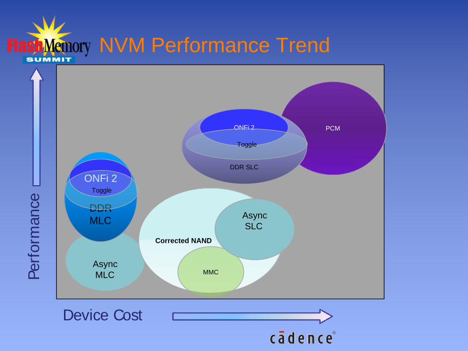
NVM Performance Trend
AsyncMLC
Corrected NAND
MMC
DDR MLC
PCM
DDR SLC
ONFi 2
Toggle
AsyncSLC
Perf
orm
ance
ONFi 2Toggle
Device Cost
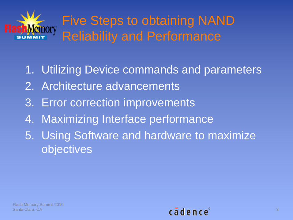
Five Steps to obtaining NAND Reliability and Performance
1. Utilizing Device commands and parameters2. Architecture advancements3. Error correction improvements 4. Maximizing Interface performance5. Using Software and hardware to maximize
objectives
Flash Memory Summit 2010Santa Clara, CA 3
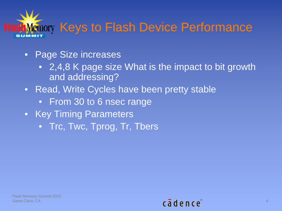
Keys to Flash Device Performance
Flash Memory Summit 2010Santa Clara, CA 4
• Page Size increases• 2,4,8 K page size What is the impact to bit growth
and addressing?• Read, Write Cycles have been pretty stable
• From 30 to 6 nsec range• Key Timing Parameters
• Trc, Twc, Tprog, Tr, Tbers
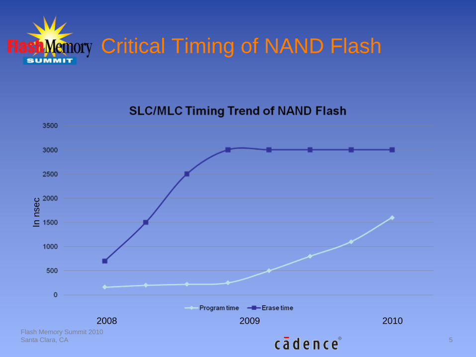
Critical Timing of NAND Flash
Flash Memory Summit 2010Santa Clara, CA 5
In n
sec
2008 2009 2010
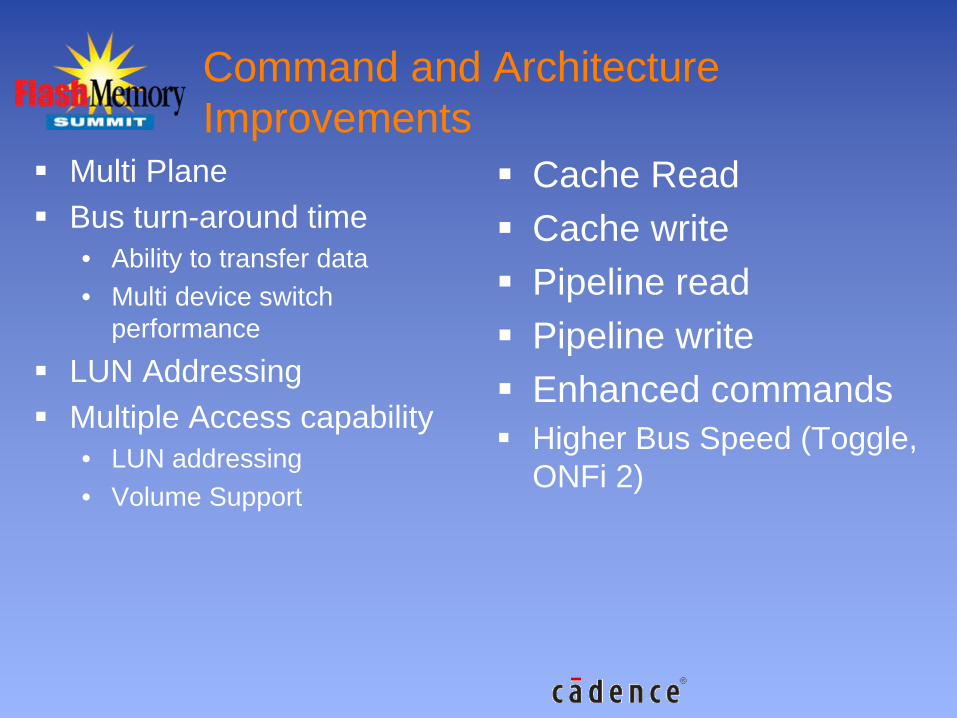
Command and Architecture Improvements
Multi PlaneBus turn-around time•
Ability to transfer data•
Multi device switch performance
LUN AddressingMultiple Access capability•
LUN addressing•
Volume Support
Cache ReadCache writePipeline readPipeline writeEnhanced commandsHigher Bus Speed (Toggle, ONFi 2)
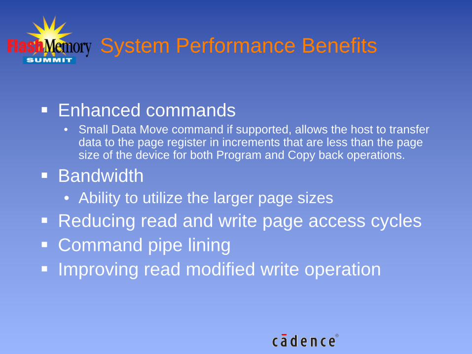
Enhanced commands•
Small Data Move command if supported, allows the host to transfer data to the page register in increments that are less than the page size of the device for both Program and Copy back operations.
Bandwidth•
Ability to utilize the larger page sizes
Reducing read and write page access cyclesCommand pipe liningImproving read modified write operation
System Performance Benefits
Mic
rose
cond
s
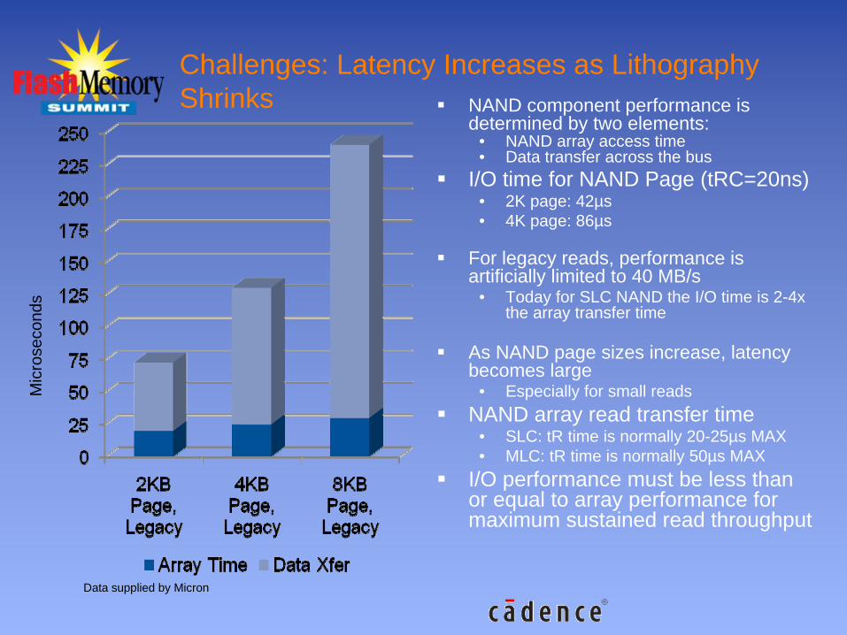
NAND component performance is determined by two elements:•
NAND array access time•
Data transfer across the busI/O time for NAND Page (tRC=20ns)•
2K page: 42µs•
4K page: 86µs
For legacy reads, performance is artificially limited to 40 MB/s•
Today for SLC NAND the I/O time is 2-4x the array transfer time
As NAND page sizes increase, latency becomes large•
Especially for small readsNAND array read transfer time•
SLC: tR time is normally 20-25µs MAX•
MLC: tR time is normally 50µs MAXI/O performance must be less than or equal to array performance for maximum sustained read throughput
Challenges: Latency Increases as Lithography Shrinks
Data supplied by Micron
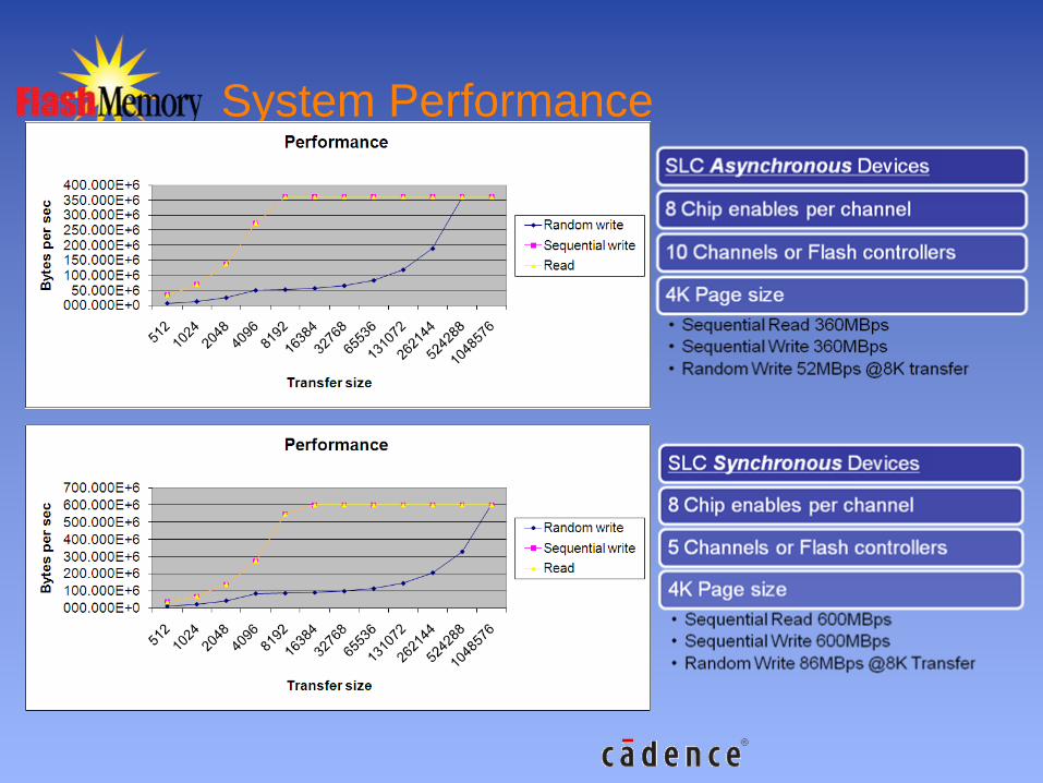
System Performance
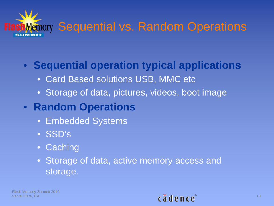
Sequential vs. Random Operations
• Sequential operation typical applications• Card Based solutions USB, MMC etc• Storage of data, pictures, videos, boot image
• Random Operations• Embedded Systems• SSD’s• Caching• Storage of data, active memory access and
storage.
Flash Memory Summit 2010Santa Clara, CA 10
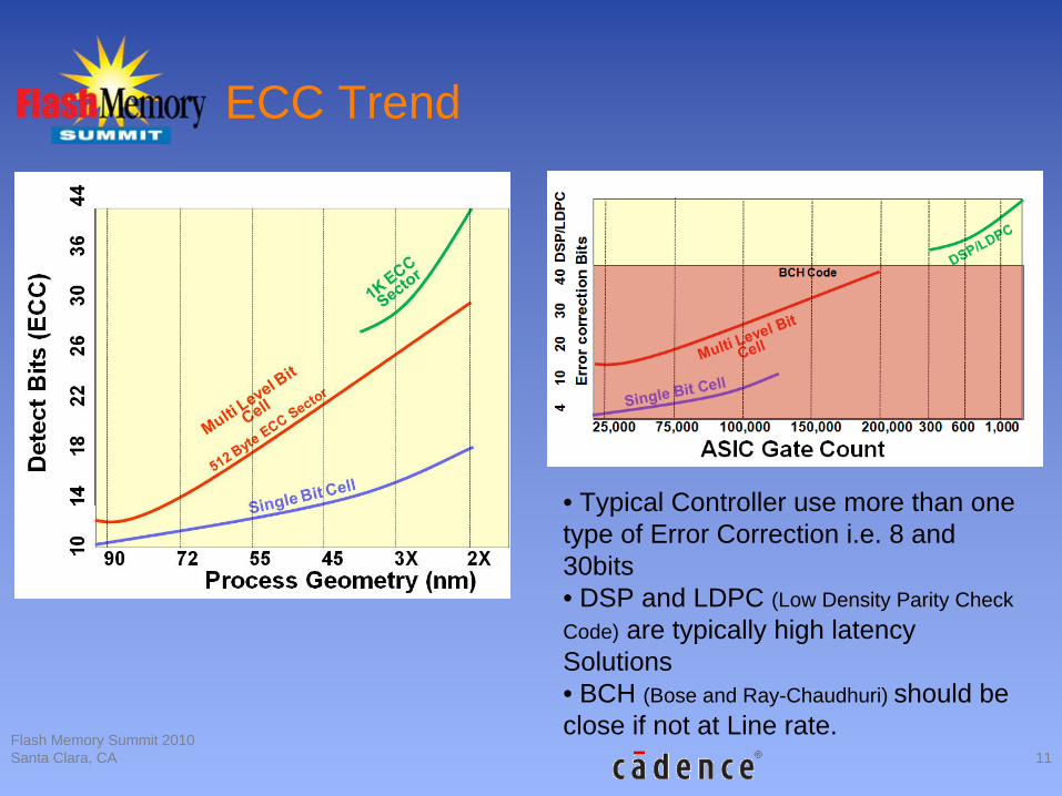
ECC Trend
Flash Memory Summit 2010Santa Clara, CA 11
• Typical Controller use more than one type of Error Correction i.e. 8 and 30bits• DSP and LDPC (Low Density Parity Check Code) are typically high latency Solutions• BCH (Bose and Ray-Chaudhuri) should be close if not at Line rate.
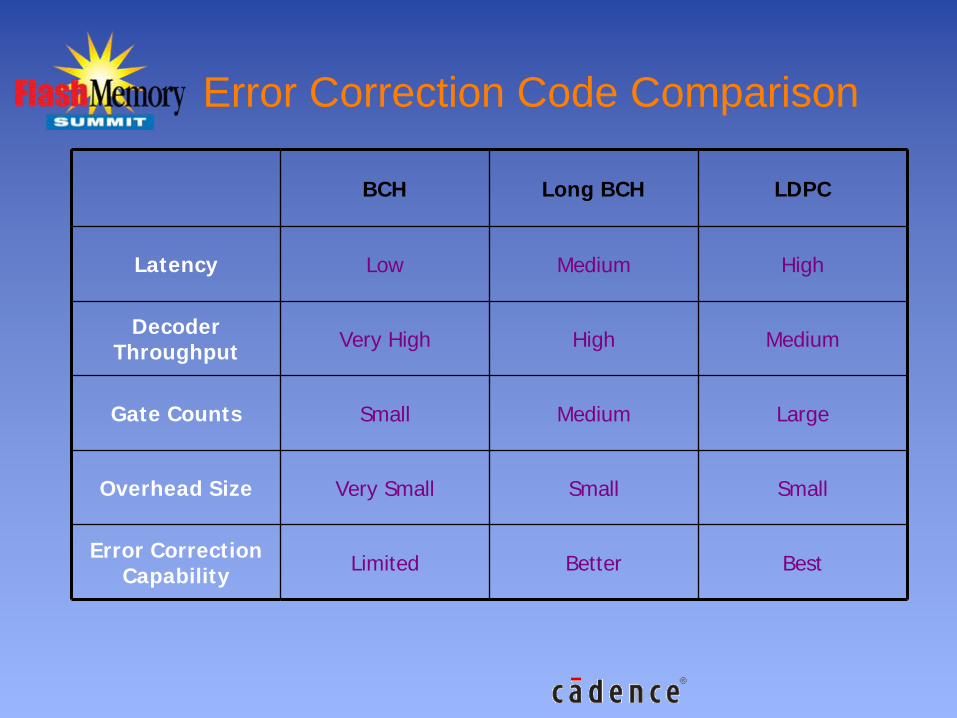
BCH Long BCH LDPC
Latency Low Medium High
Decoder Throughput Very High High Medium
Gate Counts Small Medium Large
Overhead Size Very Small Small Small
Error Correction Capability Limited Better Best
Error Correction Code Comparison
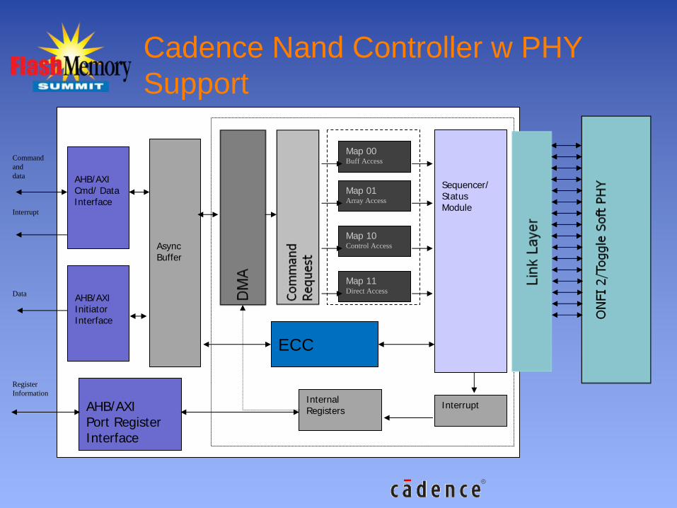
Cadence Nand Controller w PHY Support
Map 00Buff Access
Map 01Array Access
Map 10Control Access
Map 11Direct Access
Internal Registers Interrupt
Sequencer/StatusModule
Async Buffer
AHB/AXICmd/ Data Interface
AHB/AXIPort RegisterInterface
Commandanddata
Interrupt
Data
Register Information
ECC
AHB/AXIInitiator Interface
Centralized LDPC Hardware Architecture
ProcessorProcessor
HOSTSYSTEMHOSTSYSTEM
Host InterfaceController
Host InterfaceController
DMADMA
RAMControllerRAMController
BUFFERBUFFER
PHY
PHY
1 … x NAND Devices
1 … x NAND Devices
1 … x NAND Devices
1 … x NAND Devices
1 … x NAND Devices
1 … x NAND Devices
NANDControllerChannel n
NANDControllerChannel n
NANDControllerChannel 1
NANDControllerChannel 1
NANDControllerChannel 2
NANDControllerChannel 2
CMD &DATADMA
CMD &DATADMA
CMD &DATADMA
CMD &DATADMA
CMD &DATADMA
CMD &DATADMA
ECC,CRCOther
ECC,CRCOther
ECC,CRCOther
ECC,CRCOther
ECC,CRCOther
ECC,CRCOther
PHY
PHY
PHY
PHY
PHY
PHY
1 … x controller channels1 … x controller channels
LDPCLDPC
Multi-PortArbitrationUnit
Multi-PortArbitrationUnit
Centralized ECC Hardware Architecture
ProcessorProcessor
HOSTSYSTEMHOSTSYSTEM
Host InterfaceController
Host InterfaceController
DMADMA
RAMControllerRAMController
BUFFERBUFFER
PHY
PHY
1 … x NAND Devices
1 … x NAND Devices
1 … x NAND Devices
1 … x NAND Devices
1 … x NAND Devices
1 … x NAND Devices
NANDControllerChannel n
NANDControllerChannel n
NANDControllerChannel 1
NANDControllerChannel 1
NANDControllerChannel 2
NANDControllerChannel 2
CMD &DATADMA
CMD &DATADMA
CRCCRC
CRCCRC
CRCCRC
PHY
PHY
PHY
PHY
PHY
PHY
1 … x controller channels1 … x controller channels
LDPCLDPC
Multi-PortArbitrationUnit
Multi-PortArbitrationUnit
BCH, ECCBCH, ECC
BufferBuffer
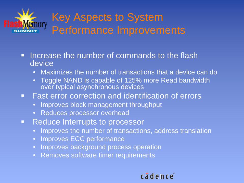
Key Aspects to System Performance Improvements
Increase the number of commands to the flash device•
Maximizes the number of transactions that a device can do•
Toggle NAND is capable of 125% more Read bandwidth over typical asynchronous devices
Fast error correction and identification of errors•
Improves block management throughput•
Reduces processor overheadReduce Interrupts to processor•
Improves the number of transactions, address translation•
Improves ECC performance•
Improves background process operation•
Removes software timer requirements
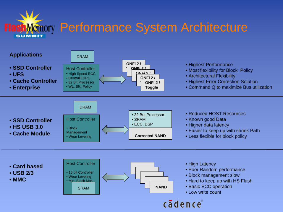
Performance System Architecture
Host Controller• High Speed ECC• Central LDPC• 32 Bit Processor• WL, Blk. Policy
DRAM
ONFi 2 / ToggleONFi 2 /
ToggleONFi 2 / ToggleONFi 2 /
ToggleONFi 2 / Toggle
• Highest Performance• Most flexibility for Block Policy• Architectural Flexibility• Highest Error Correction Solution• Command Q to maximize Bus utilization
Host Controller
• Block Management• Wear Leveling
DRAM
Corrected NAND
• 32 But Processor• SRAM• ECC, DSP
• Reduced HOST Resources• Known good Data• Higher data latency• Easier to keep up with shrink Path• Less flexible for block policy
Host Controller
• 16 bit Controller• Wear Leveling• Min. Block Mgr.
SRAM
NANDNAND
NANDNAND
NAND
• High Latency• Poor Random performance• Block management slow• Hard to keep up with HS Flash• Basic ECC operation• Low write count
Applications
• SSD Controller• UFS • Cache Controller• Enterprise
• SSD Controller• HS USB 3.0• Cache Module
• Card based• USB 2/3• MMC
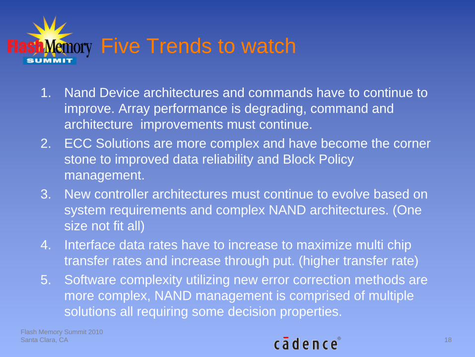
Five Trends to watch
1. Nand Device architectures and commands have to continue to improve. Array performance is degrading, command and architecture improvements must continue.
2. ECC Solutions are more complex and have become the corner stone to improved data reliability and Block Policy management.
3. New controller architectures must continue to evolve based on system requirements and complex NAND architectures. (One size not fit all)
4. Interface data rates have to increase to maximize multi chip transfer rates and increase through put. (higher transfer rate)
5. Software complexity utilizing new error correction methods are more complex, NAND management is comprised of multiple solutions all requiring some decision properties.
Flash Memory Summit 2010Santa Clara, CA 18