"flexible display enabling technology," spie 4362
TRANSCRIPT
Flexible display enabling technology
Sigurd Wagnera*, Stephen J. Fonashb**, Thomas N. Jacksonb***, James C. Sturma****
aPrinceton University, bPennsylvania State University
ABSTRACT In a collaboration between Pennsylvania State University and Princeton University, we have been laying the foundations for flexible display technology. Flexible substrates including plastic or steel foil, backplanes of organic or silicon transistors, and directly printed RGB organic light emitting diodes are issues central to this collaboration. We present an overview of key recent results. Silicon based thin film transistors have been processed at the ultralow temperatures required for processing on plastic substrates. Organic thin film transistors and circuits with record mobilities have been fabricated that are naturally matched to low temperature substrates. Organic light emitting diodes have been made by inkjet printing in an approach that solves the RGB patterning problem of OLED displays. The mechanics of flexible substrates have been defined and thin film silicon transistor performance is shown to be unaffected by bending. Substantial progress has been made toward the realization of rugged, lightweight, flexible and even conformal displays.
1. INTRODUCTION Displays that combine light weight with flexibility, and displays that conform to curved surfaces, are essential to many DOD applications. Light weight and flexibility makes displays inherently rugged and thus ensure dependable presentation of information in the field. Conformal displays do confer dual-function capability, for example as transparent overlays on cockpit canopies or stick-on displays attached to the structure of vehicles. Such displays have a number of common technical attributes: thin foil substrates, thin film electronics, and capability to extend over large surface areas. In a collaboration of four research groups we have been laying the groundwork for this technology[1]. We have reported highlights of the results obtained by our collaboration at an earlier SPIE Conference[2]. This paper presents some of our recent progress. Two kinds of thin foil qualify as substrate for flexible displays: foils of organic polymers ("plastics") and metal foils. Simple mechanical rules can be developed for building thin film circuits on foils in structures that are forgiving of mechanical stress. Recent interest has focused on the fabrication of circuits on plastic foil. Two of our projects focus on the fabrication of silicon based transistor electronics on plastic substrates. Their central aspect is reduction of all process temperatures below the strain points of the plastic substrates. This reduction requires considerable process innovation and modification. One of these projects is oriented toward new techniques for reaching very low silicon process temperatures. The other project serves to understand the mechano-electrical performance of thin film silicon transistors made on plastic foils. Organic thin-film electronics is a highly promising alternative to silicon electronics. Organic compounds are synthesized and processed at low temperatures, and frequently are unstable against moderately high temperatures. Thus organic semiconductors are natural candidates for low-temperature electronics, including transistor electronics and light emitting diodes. Furthermore, organic electronics are viewed to *[email protected]; phone 1 609 258 4631; fax 1 609 258 6279; Department of Electrical Engineering, Princeton University, Princeton, NJ 08544; **[email protected]; phone 1 814 865 4931; fax 1 814 865 3018; Electronic Materials & Processing Laboratory, Pennsylvania State University, 189 MRI Building, University Park, PA 16802; ***[email protected]; phone 1 814 865 7667; fax 1 814 863 5241; Department of Electrical Engineering, Pennsylvania State University, 216 West Building, University Park, PA 16802; ****[email protected]; phone 1 609 258 5610; fax 1 609 258 1954; Center for Photonic and Optoelectronic Materials, Princeton, NJ 08544.
Proc. SPIE 4362, 226-244 (2001), presented at SPIE Symp., Orlando, FL (April, 2001)
be a natural match for plastic substrates. One of our projects focuses on the fabrication of organic-molecule thin film transistors, and another on the fabrication of organic-polymer light emitting diodes. Even though specialized applications may tolerate substantial cost, in the long term low cost will be crucial for sustained technology development. Our premise has been that cost reduction will come primarily through the reduction in the number of process steps, and later on through the reduction of materials consumption during fabrication and in the product. Direct printing of device materials is a very efficient approach toward the reduction of the number of process steps. One of our projects employs inkjet printing for the fabrication of organic light emitting diodes in the three primary colors, red, green and blue. Another project is devoted to the direct printing of metalization using inkjet and imprinting. In this paper we focus on four of our projects: (1) techniques for fabricating silicon transistor materials at temperatures below 100°C; (2) the fabrication of organic thin film transistors and circuits; (3) the use of inkjet printing in the fabrication of organic RGB light emitting diodes; and (4) the dependence on mechanical strain of the electrical performance of silicon thin film transistors made on plastic substrates.
2. LOW TEMPERATURE PROCESSES FOR THIN FILM SILICON TRANSISTORS AND A NOVEL SEPARATION TECHNOLOGY
2.1 Development of low-temperature micro-crystalline silicon TFTs
This approach, the most basic, uses the direct low-temperature deposition of microcrystalline silicon (mc-Si) using high-density plasmas (HDP). We have already been successful fabricating TFTs with this approach using glass substrates; hence our goal is one of transferring the approach to plastic substrates and of broadening, refinement, and enhancement.
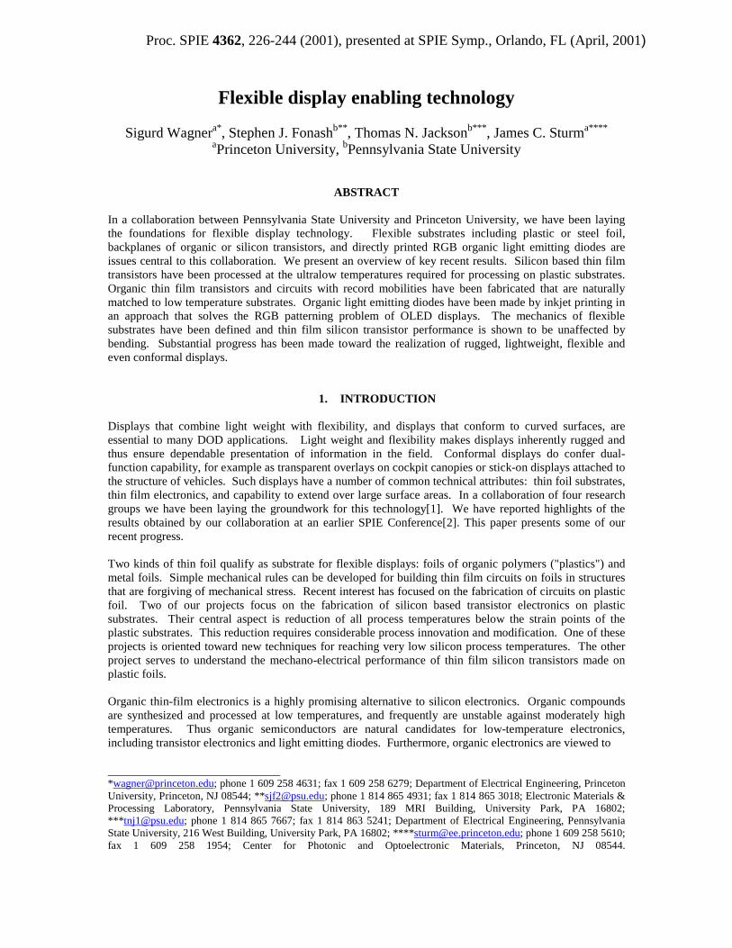
In the demonstration we did on glass substrates, the NMOS TFTs of Fig. 1 were fabricated using processing temperatures at or below 340 oC. The n-type doped silicon, silicon dioxide gate dielectric, and intrinsic silicon layers were all deposited using the same ECR-PECVD system. Only two masks were used and no critical etch steps were involved. The source and drain (S/D) regions were patterned by contact lithography and the patterns were defined by reactive ion etching. The conductivity of the n-type source/drain material was in the range of 1-10 S/cm when the n-type layer even was deposited at < 285 oC. The crystallinity of the silicon layers was verified by X-ray diffraction, Raman spectroscopy and UV reflectance spectroscopy[3].
Figure 1. Schematic of mc-Si TFT fabricated using the processing scheme described in the text. The layers in the center of the TFT are deposited on glass in the sequence of a passivation silicon nitride, the intrinsic microcrystalline
silicon, and a silicon oxide gate dielectric.
Gate metal S/D metal
N poly N poly
S/D metal
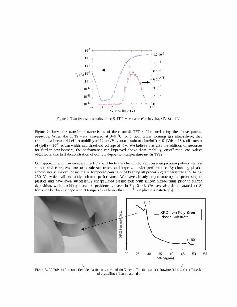
Figure 2. Transfer characteristics of mc-Si TFTs when source/drain voltage (Vds) = 1 V.
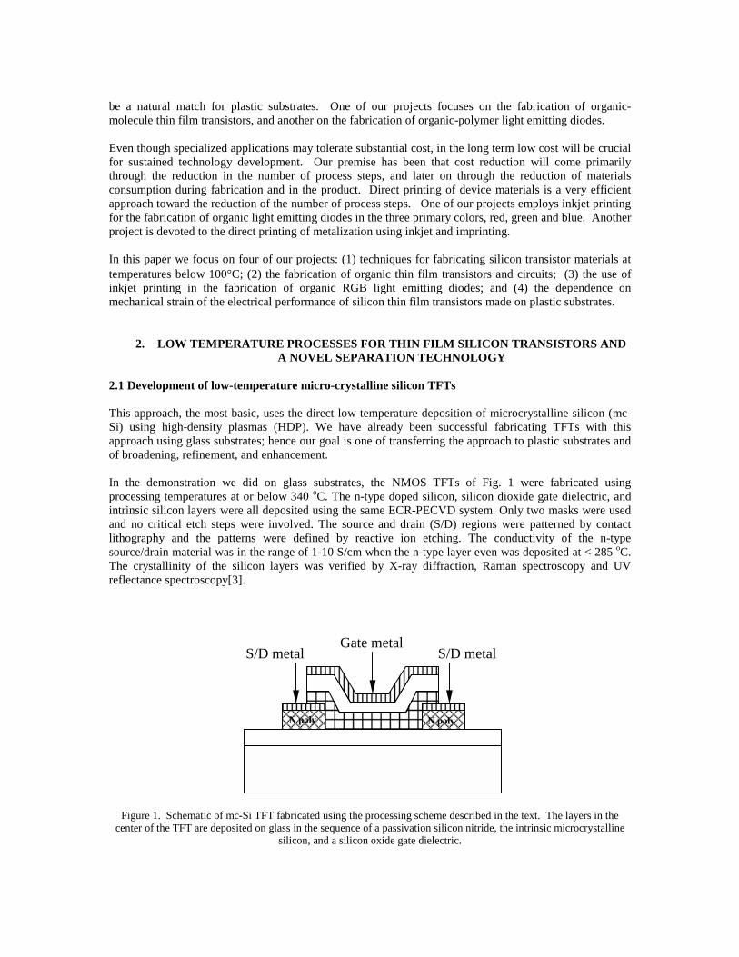
Figure 2 shows the transfer characteristics of these mc-Si TFT s fabricated using the above process sequence. When the TFTs were annealed at 340 oC for 1 hour under forming gas atmosphere, they exhibited a linear field effect mobility of 12 cm2/V-s, on/off ratio of (Ion/Ioff) >106 (Vds = 1V), off current of (Ioff) < 10-12 A/µm width, and threshold voltage of 5V. We believe that with the addition of resources for further development, the performance can improved above these mobility, on/off ratio, etc. values obtained in this first demonstration of our low deposition temperature mc-Si TFTs.
Our approach with low-temperature HDP will be to transfer this low process-temperature poly-crystalline silicon device process flow to plastic substrates, and improve device performance. By choosing plastics appropriately, we can loosen the self-imposed constraint of keeping all processing temperatures at or below 250 oC, which will certainly enhance performance. We have already begun moving the processing to plastics and have even successfully encapsulated plastic foils with silicon nitride films prior to silicon deposition, while avoiding distortion problems, as seen in Fig. 3 [4]. We have also demonstrated mc-Si films can be directly deposited at temperatures lower than 130 oC on plastic substrates[5].
(a) (b) Figure 3. (a) Poly-Si film on a flexible plastic substrate and (b) X-ray diffraction pattern showing (111) and (110) peaks
of crystalline silicon materials.
0
1000
2000
3000
4000
5000
6000
7000
8000
20 25 30 35 40 45 50 55
XRD from Poly-Si on Plastic Substrate
(111)
(110)
2θ (degree)
10 -12 10 -11
-10 10 -9 10 -8 10 -7 10 -6 10 -5
0
2 10-7
4 10-7
6 10-7
8 10-7
1 10-6
1.2 10 -6
-2 0 2 4 6 8 10
10
ID (A) S
Gate Voltage (V)
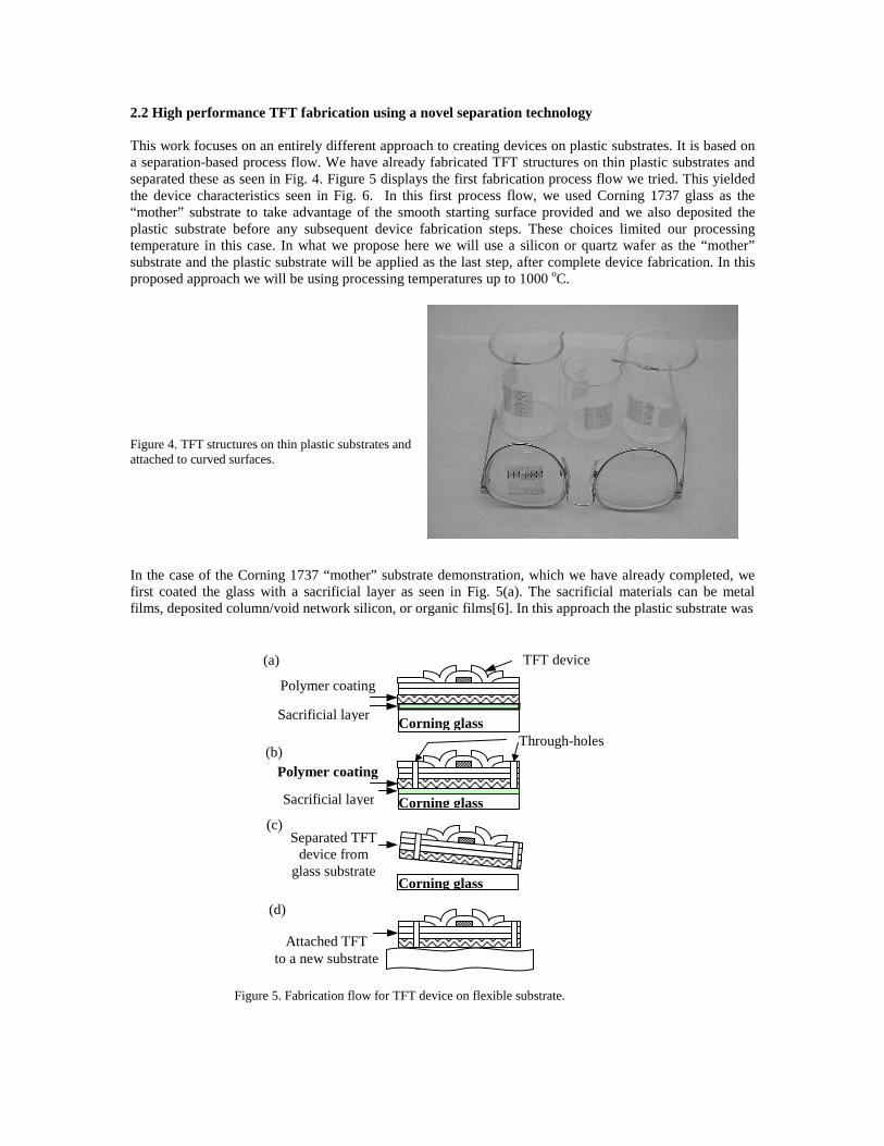
2.2 High performance TFT fabrication using a novel separation technology This work focuses on an entirely different approach to creating devices on plastic substrates. It is based on a separation-based process flow. We have already fabricated TFT structures on thin plastic substrates and separated these as seen in Fig. 4. Figure 5 displays the first fabrication process flow we tried. This yielded the device characteristics seen in Fig. 6. In this first process flow, we used Corning 1737 glass as the “mother” substrate to take advantage of the smooth starting surface provided and we also deposited the plastic substrate before any subsequent device fabrication steps. These choices limited our processing temperature in this case. In what we propose here we will use a silicon or quartz wafer as the “mother” substrate and the plastic substrate will be applied as the last step, after complete device fabrication. In this proposed approach we will be using processing temperatures up to 1000 oC. Figure 4. TFT structures on thin plastic substrates and attached to curved surfaces. In the case of the Corning 1737 “mother” substrate demonstration, which we have already completed, we first coated the glass with a sacrificial layer as seen in Fig. 5(a). The sacrificial materials can be metal films, deposited column/void network silicon, or organic films[6]. In this approach the plastic substrate was
Figure 5. Fabrication flow for TFT device on flexible substrate.
Corning glass
Polymer coating
Sacrificial layer
(a)
Corning glass
Polymer coating
Sacrificial layer
Through-holes(b)
Corning glass
Separated TFTdevice from
glass substrate
(c)
(d)
Rugged flexible Attached TFT
to a new substrate
TFT device
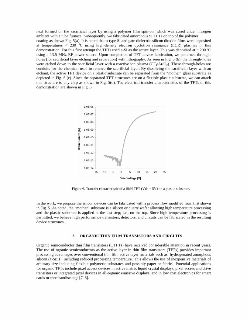
next formed on the sacrificial layer by using a polymer film spin-on, which was cured under nitrogen ambient with a tube furnace. Subsequently, we fabricated amorphous Si TFTs on top of the polymer coating as shown Fig. 5(a). It is noted that n-type Si and gate dielectric silicon dioxide films were deposited at temperatures < 230 oC using high-density electron cyclotron resonance (ECR) plasmas in this demonstration. For this first attempt the TFTs used a-Si as the active layer. This was deposited at ~ 200 oC using a 13.5 MHz RF power source. Upon completion of TFT device fabrication, we patterned through-holes (for sacrificial layer etching and separation) with lithography. As seen in Fig. 5 (b), the through-holes were etched down to the sacrificial layer with a reactive ion plasma (CF4/Ar/O2). These through-holes are conduits for the chemical used to remove the sacrificial layer. By dissolving the sacrificial layer with an etchant, the active TFT device on a plastic substrate can be separated from the “mother” glass substrate as depicted in Fig. 5 (c). Since the separated TFT structures are on a flexible plastic substrate, we can attach this structure to any chip as shown in Fig. 5(d). The electrical transfer characteristics of the TFTs of this demonstration are shown in Fig. 6.
Figure 6. Transfer characteristic of a-Si:H TFT (Vds = 5V) on a plastic substrate.
In the work, we propose the silicon devices can be fabricated with a process flow modified from that shown in Fig. 5. As noted, the “mother” substrate is a silicon or quartz wafer allowing high temperature processing and the plastic substrate is applied at the last step; i.e., on the top. Since high temperature processing is permitted, we believe high performance transistors, detectors, and circuits can be fabricated in the resulting device structures.
3. ORGANIC THIN FILM TRANSISTORS AND CIRCUITS
Organic semiconductor thin film transistors (OTFTs) have received considerable attention in recent years. The use of organic semiconductors as the active layer in thin film transistors (TFTs) provides important processing advantages over conventional thin film active layer materials such as hydrogenated amorphous silicon (a-Si:H), including reduced processing temperature. This allows the use of inexpensive materials of arbitrary size including flexible polymeric substrates and possibly paper or fabric. Potential applications for organic TFTs include pixel access devices in active matrix liquid crystal displays, pixel access and drive transistors or integrated pixel devices in all-organic emissive displays, and in low cost electronics for smart cards or merchandise tags [7, 8].
1.0E-14
1.0E-13
1.0E-12
1.0E-11
1.0E-10
1.0E-09
1.0E-08
1.0E-07
1.0E-06
-15 -10 -5 0 5 10 15 20 25
Gate Voltage [V]
Dra
in C
urre
nt [A
]
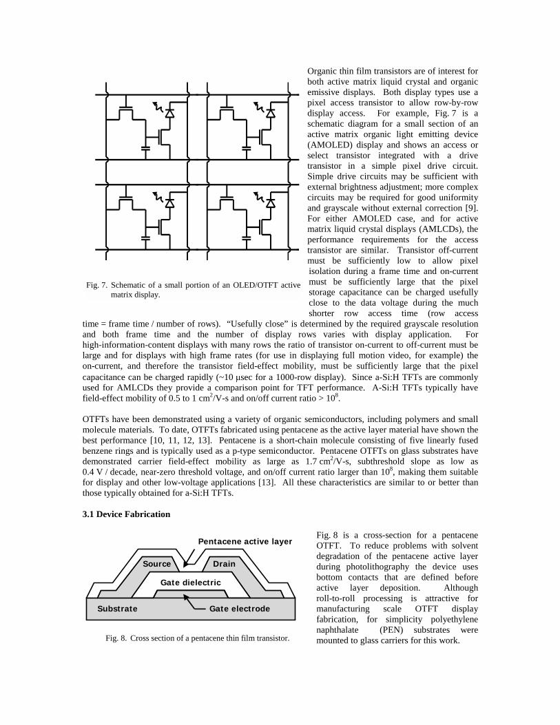
Organic thin film transistors are of interest for both active matrix liquid crystal and organic emissive displays. Both display types use a pixel access transistor to allow row-by-row display access. For example, Fig. 7 is a schematic diagram for a small section of an active matrix organic light emitting device (AMOLED) display and shows an access or select transistor integrated with a drive transistor in a simple pixel drive circuit. Simple drive circuits may be sufficient with external brightness adjustment; more complex circuits may be required for good uniformity and grayscale without external correction [9]. For either AMOLED case, and for active matrix liquid crystal displays (AMLCDs), the performance requirements for the access transistor are similar. Transistor off-current must be sufficiently low to allow pixel isolation during a frame time and on-current must be sufficiently large that the pixel storage capacitance can be charged usefully close to the data voltage during the much shorter row access time (row access
time = frame time / number of rows). “Usefully close” is determined by the required grayscale resolution and both frame time and the number of display rows varies with display application. For high-information-content displays with many rows the ratio of transistor on-current to off-current must be large and for displays with high frame rates (for use in displaying full motion video, for example) the on-current, and therefore the transistor field-effect mobility, must be sufficiently large that the pixel capacitance can be charged rapidly (~10 µsec for a 1000-row display). Since a-Si:H TFTs are commonly used for AMLCDs they provide a comparison point for TFT performance. A-Si:H TFTs typically have field-effect mobility of 0.5 to 1 cm2/V-s and on/off current ratio > 108. OTFTs have been demonstrated using a variety of organic semiconductors, including polymers and small molecule materials. To date, OTFTs fabricated using pentacene as the active layer material have shown the best performance [10, 11, 12, 13]. Pentacene is a short-chain molecule consisting of five linearly fused benzene rings and is typically used as a p-type semiconductor. Pentacene OTFTs on glass substrates have demonstrated carrier field-effect mobility as large as 1.7 cm2/V-s, subthreshold slope as low as 0.4 V / decade, near-zero threshold voltage, and on/off current ratio larger than 108, making them suitable for display and other low-voltage applications [13]. All these characteristics are similar to or better than those typically obtained for a-Si:H TFTs. 3.1 Device Fabrication
Fig. 8 is a cross-section for a pentacene OTFT. To reduce problems with solvent degradation of the pentacene active layer during photolithography the device uses bottom contacts that are defined before active layer deposition. Although roll-to-roll processing is attractive for manufacturing scale OTFT display fabrication, for simplicity polyethylene naphthalate (PEN) substrates were mounted to glass carriers for this work.
Fig. 7. Schematic of a small portion of an OLED/OTFT activematrix display.
Substrate Gate electrode
Pentacene active layer
Gate dielectric
Source Drain
Fig. 8. Cross section of a pentacene thin film transistor.
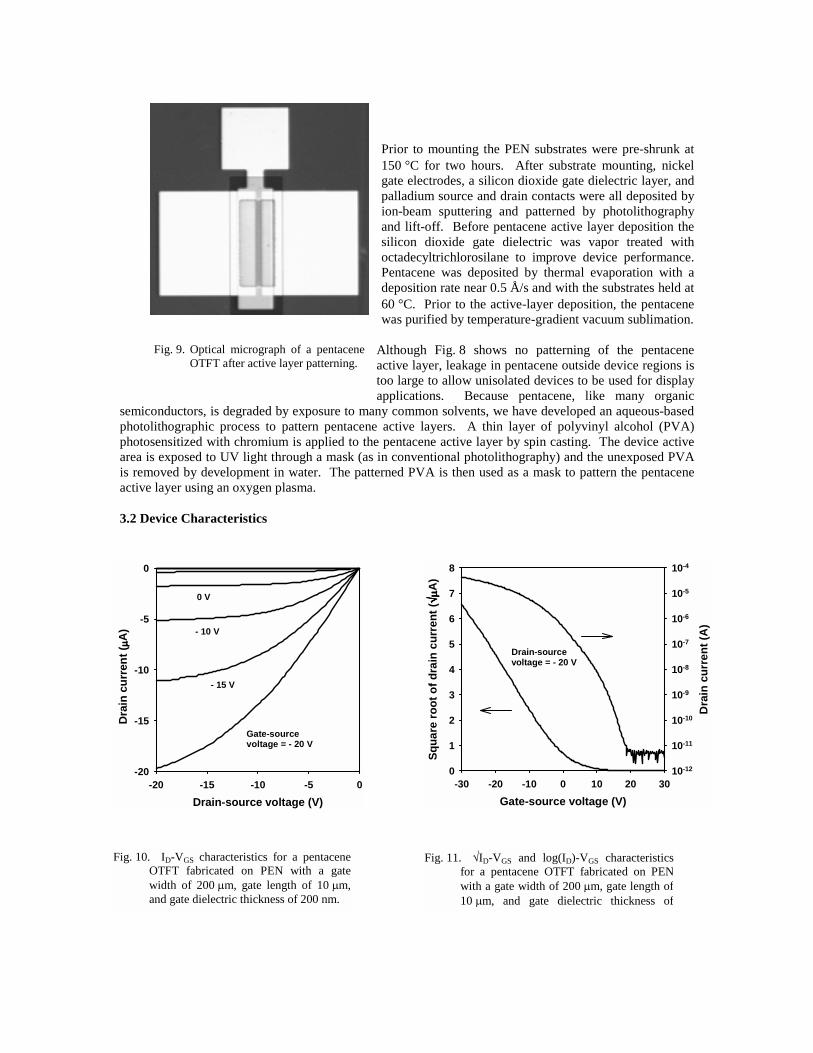
Prior to mounting the PEN substrates were pre-shrunk at 150 °C for two hours. After substrate mounting, nickel gate electrodes, a silicon dioxide gate dielectric layer, and palladium source and drain contacts were all deposited by ion-beam sputtering and patterned by photolithography and lift-off. Before pentacene active layer deposition the silicon dioxide gate dielectric was vapor treated with octadecyltrichlorosilane to improve device performance. Pentacene was deposited by thermal evaporation with a deposition rate near 0.5 Å/s and with the substrates held at 60 °C. Prior to the active-layer deposition, the pentacene was purified by temperature-gradient vacuum sublimation.
Although Fig. 8 shows no patterning of the pentacene active layer, leakage in pentacene outside device regions is too large to allow unisolated devices to be used for display applications. Because pentacene, like many organic
semiconductors, is degraded by exposure to many common solvents, we have developed an aqueous-based photolithographic process to pattern pentacene active layers. A thin layer of polyvinyl alcohol (PVA) photosensitized with chromium is applied to the pentacene active layer by spin casting. The device active area is exposed to UV light through a mask (as in conventional photolithography) and the unexposed PVA is removed by development in water. The patterned PVA is then used as a mask to pattern the pentacene active layer using an oxygen plasma. 3.2 Device Characteristics
Drain-source voltage (V)-20 -15 -10 -5 0
Dra
in c
urre
nt ( µµ µµ
A)
-20
-15
-10
-5
0
Gate-sourcevoltage = - 20 V
- 15 V
- 10 V
0 V
Fig. 11. √ID-VGS and log(ID)-VGS characteristicsfor a pentacene OTFT fabricated on PENwith a gate width of 200 µm, gate length of10 µm, and gate dielectric thickness of
Gate-source voltage (V)-30 -20 -10 0 10 20 30
Squa
re ro
ot o
f dra
in c
urre
nt ( √√ √√
µµ µµA
)
0
1
2
3
4
5
6
7
8
Dra
in c
urre
nt (A
)
10-12
10-11
10-10
10-9
10-8
10-7
10-6
10-5
10-4
Drain-sourcevoltage = - 20 V
Fig. 10. ID-VGS characteristics for a pentaceneOTFT fabricated on PEN with a gatewidth of 200 µm, gate length of 10 µm,and gate dielectric thickness of 200 nm.
Fig. 9. Optical micrograph of a pentaceneOTFT after active layer patterning.
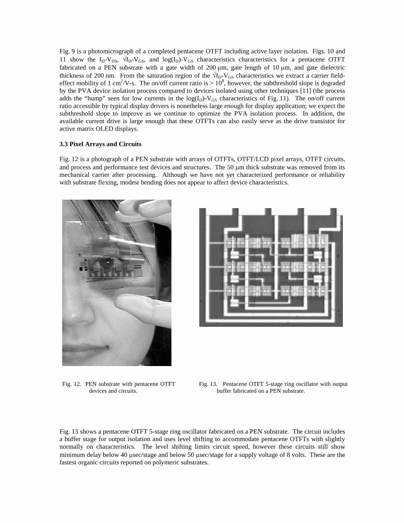
Fig. 9 is a photomicrograph of a completed pentacene OTFT including active layer isolation. Figs. 10 and 11 show the ID-VDS, √ID-VGS, and log(ID)-VGS characteristics characteristics for a pentacene OTFT fabricated on a PEN substrate with a gate width of 200 µm, gate length of 10 µm, and gate dielectric thickness of 200 nm. From the saturation region of the √ID-VGS characteristics we extract a carrier field-effect mobility of 1 cm2/V-s. The on/off current ratio is > 108, however, the subthreshold slope is degraded by the PVA device isolation process compared to devices isolated using other techniques [11] (the process adds the “hump” seen for low currents in the log(ID)-VGS characteristics of Fig. 11). The on/off current ratio accessible by typical display drivers is nonetheless large enough for display application; we expect the subthreshold slope to improve as we continue to optimize the PVA isolation process. In addition, the available current drive is large enough that these OTFTs can also easily serve as the drive transistor for active matrix OLED displays. 3.3 Pixel Arrays and Circuits Fig. 12 is a photograph of a PEN substrate with arrays of OTFTs, OTFT/LCD pixel arrays, OTFT circuits, and process and performance test devices and structures. The 50 µm thick substrate was removed from its mechanical carrier after processing. Although we have not yet characterized performance or reliability with substrate flexing, modest bending does not appear to affect device characteristics.
Fig. 13 shows a pentacene OTFT 5-stage ring oscillator fabricated on a PEN substrate. The circuit includes a buffer stage for output isolation and uses level shifting to accommodate pentacene OTFTs with slightly normally on characteristics. The level shifting limits circuit speed, however these circuits still show minimum delay below 40 µsec/stage and below 50 µsec/stage for a supply voltage of 8 volts. These are the fastest organic circuits reported on polymeric substrates.
Fig. 12. PEN substrate with pentacene OTFTdevices and circuits.
Fig. 13. Pentacene OTFT 5-stage ring oscillator with outputbuffer fabricated on a PEN substrate.
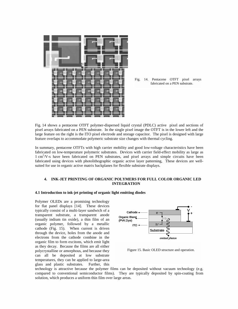
Fig. 14 shows a pentacene OTFT polymer-dispersed liquid crystal (PDLC) active pixel and sections of pixel arrays fabricated on a PEN substrate. In the single pixel image the OTFT is in the lower left and the large feature on the right is the ITO pixel electrode and storage capacitor. The pixel is designed with large feature overlaps to accommodate polymeric substrate size changes with thermal cycling. In summary, pentacene OTFTs with high carrier mobility and good low-voltage characteristics have been fabricated on low-temperature polymeric substrates. Devices with carrier field-effect mobility as large as 1 cm2/V-s have been fabricated on PEN substrates, and pixel arrays and simple circuits have been fabricated using devices with photolithographic organic active layer patterning, These devices are well-suited for use in organic active matrix backplanes for flexible substrate displays.
4. INK-JET PRINTING OF ORGANIC POLYMERS FOR FULL COLOR ORGANIC LED
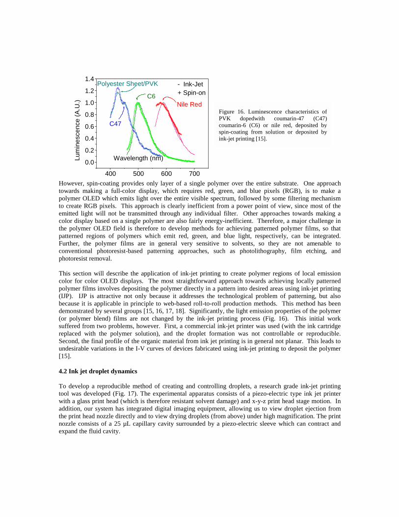
INTEGRATION 4.1 Introduction to ink-jet printing of organic light emitting diodes Polymer OLEDs are a promising technology for flat panel displays [14]. These devices typically consist of a multi-layer sandwich of a transparent substrate, a transparent anode (usually indium tin oxide), a thin film of an organic polymer, followed by a metallic cathode (Fig. 15). When current is driven through the device, holes from the anode and electrons from the cathode combine in the organic film to form excitons, which emit light as they decay. Because the films are all either polycrystalline or amorphous, and because they can all be deposited at low substrate temperatures, they can be applied to large-area glass and plastic substrates. Further, this technology is attractive because the polymer films can be deposited without vacuum technology (e.g. compared to conventional semiconductor films). They are typically deposited by spin-coating from solution, which produces a uniform thin film over large areas.
Figure 15. Basic OLED structure and operation.
SubstrateITO
Organic Blend(PVK:Dye)
Cathode
h+
e-
-
+V
emitted photon
SubstrateITO
Organic Blend(PVK:Dye)
Cathode
h+
e-
-
+V
emitted photon
Fig. 14. Pentacene OTFT pixel arraysfabricated on a PEN substrate.
Figure 15. Basic OLED structure and operation.
However, spin-coating provides only layer of a single polymer over the entire substrate. One approach towards making a full-color display, which requires red, green, and blue pixels (RGB), is to make a polymer OLED which emits light over the entire visible spectrum, followed by some filtering mechanism to create RGB pixels. This approach is clearly inefficient from a power point of view, since most of the emitted light will not be transmitted through any individual filter. Other approaches towards making a color display based on a single polymer are also fairly energy-inefficient. Therefore, a major challenge in the polymer OLED field is therefore to develop methods for achieving patterned polymer films, so that patterned regions of polymers which emit red, green, and blue light, respectively, can be integrated. Further, the polymer films are in general very sensitive to solvents, so they are not amenable to conventional photoresist-based patterning approaches, such as photolithography, film etching, and photoresist removal.
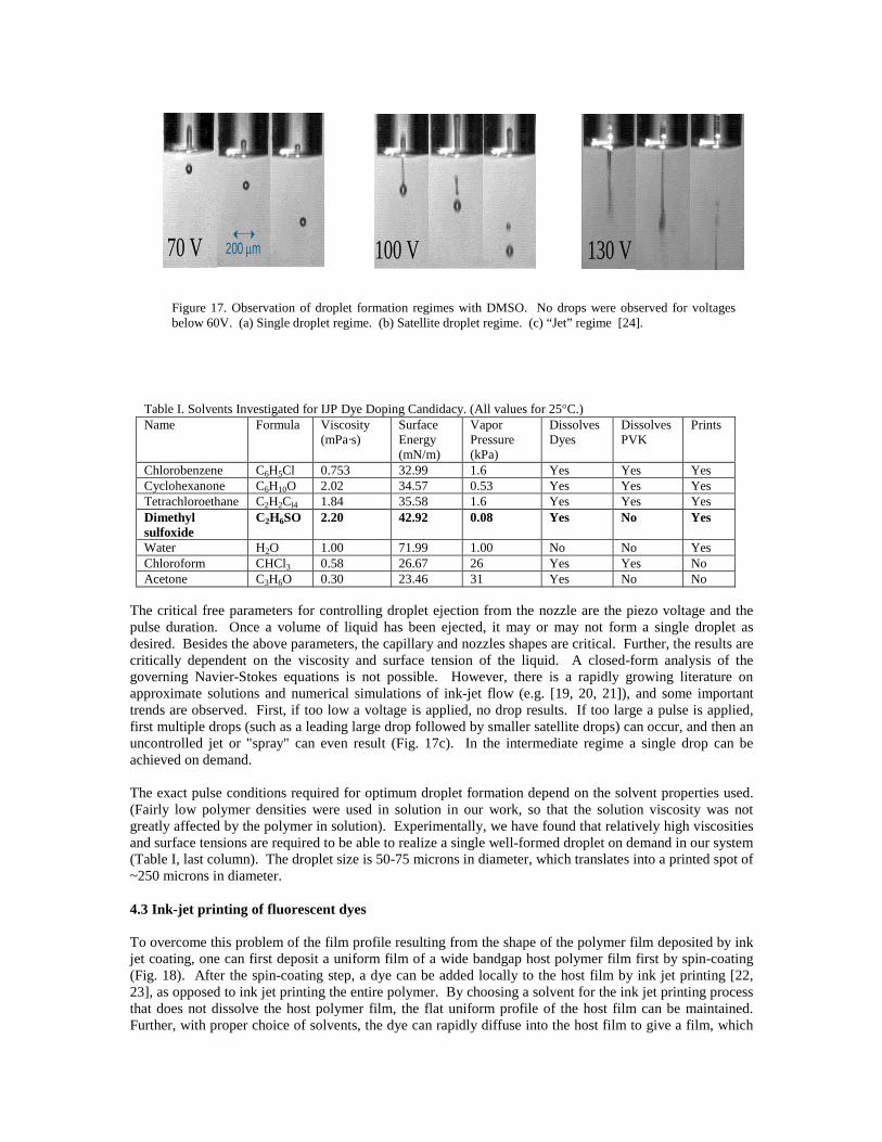
This section will describe the application of ink-jet printing to create polymer regions of local emission color for color OLED displays. The most straightforward approach towards achieving locally patterned polymer films involves depositing the polymer directly in a pattern into desired areas using ink-jet printing (IJP). IJP is attractive not only because it addresses the technological problem of patterning, but also because it is applicable in principle to web-based roll-to-roll production methods. This method has been demonstrated by several groups [15, 16, 17, 18]. Significantly, the light emission properties of the polymer (or polymer blend) films are not changed by the ink-jet printing process (Fig. 16). This initial work suffered from two problems, however. First, a commercial ink-jet printer was used (with the ink cartridge replaced with the polymer solution), and the droplet formation was not controllable or reproducible. Second, the final profile of the organic material from ink jet printing is in general not planar. This leads to undesirable variations in the I-V curves of devices fabricated using ink-jet printing to deposit the polymer [15].
4.2 Ink jet droplet dynamics
To develop a reproducible method of creating and controlling droplets, a research grade ink-jet printing tool was developed (Fig. 17). The experimental apparatus consists of a piezo-electric type ink jet printer with a glass print head (which is therefore resistant solvent damage) and x-y-z print head stage motion. In addition, our system has integrated digital imaging equipment, allowing us to view droplet ejection from the print head nozzle directly and to view drying droplets (from above) under high magnification. The print nozzle consists of a 25 µL capillary cavity surrounded by a piezo-electric sleeve which can contract and expand the fluid cavity.
Wavelength (nm)
400 500 600 700
0.0
0.2
0.4
0.6
0.8
1.0
1.2
1.4
Nile Red C6
C47
Polyester Sheet/PVK Lu
min
esce
nce
(A.U
.) - Ink-Jet + Spin-on
Figure 16. Luminescence characteristics ofPVK dopedwith coumarin-47 (C47)coumarin-6 (C6) or nile red, deposited byspin-coating from solution or deposited byink-jet printing [15].
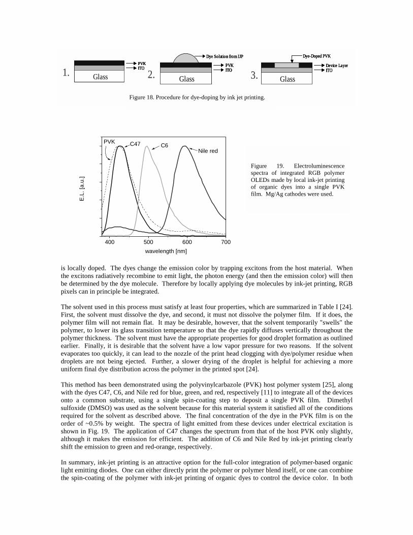
The critical free parameters for controlling droplet ejection from the nozzle are the piezo voltage and the pulse duration. Once a volume of liquid has been ejected, it may or may not form a single droplet as desired. Besides the above parameters, the capillary and nozzles shapes are critical. Further, the results are critically dependent on the viscosity and surface tension of the liquid. A closed-form analysis of the governing Navier-Stokes equations is not possible. However, there is a rapidly growing literature on approximate solutions and numerical simulations of ink-jet flow (e.g. [19, 20, 21]), and some important trends are observed. First, if too low a voltage is applied, no drop results. If too large a pulse is applied, first multiple drops (such as a leading large drop followed by smaller satellite drops) can occur, and then an uncontrolled jet or "spray" can even result (Fig. 17c). In the intermediate regime a single drop can be achieved on demand.
The exact pulse conditions required for optimum droplet formation depend on the solvent properties used. (Fairly low polymer densities were used in solution in our work, so that the solution viscosity was not greatly affected by the polymer in solution). Experimentally, we have found that relatively high viscosities and surface tensions are required to be able to realize a single well-formed droplet on demand in our system (Table I, last column). The droplet size is 50-75 microns in diameter, which translates into a printed spot of ~250 microns in diameter.
4.3 Ink-jet printing of fluorescent dyes To overcome this problem of the film profile resulting from the shape of the polymer film deposited by ink jet coating, one can first deposit a uniform film of a wide bandgap host polymer film first by spin-coating (Fig. 18). After the spin-coating step, a dye can be added locally to the host film by ink jet printing [22, 23], as opposed to ink jet printing the entire polymer. By choosing a solvent for the ink jet printing process that does not dissolve the host polymer film, the flat uniform profile of the host film can be maintained. Further, with proper choice of solvents, the dye can rapidly diffuse into the host film to give a film, which
Table I. Solvents Investigated for IJP Dye Doping Candidacy. (All values for 25°C.) Name Formula Viscosity
(mPa·s) Surface Energy (mN/m)
Vapor Pressure (kPa)
Dissolves Dyes
Dissolves PVK
Prints
Chlorobenzene C6H5Cl 0.753 32.99 1.6 Yes Yes Yes Cyclohexanone C6H10O 2.02 34.57 0.53 Yes Yes Yes Tetrachloroethane C2H2Cl4 1.84 35.58 1.6 Yes Yes Yes Dimethyl sulfoxide
C2H6SO 2.20 42.92 0.08 Yes No Yes
Water H2O 1.00 71.99 1.00 No No Yes Chloroform CHCl3 0.58 26.67 26 Yes Yes No Acetone C3H6O 0.30 23.46 31 Yes No No
(a) (b) (c)
Figure 17. Observation of droplet formation regimes with DMSO. No drops were observed for voltagesbelow 60V. (a) Single droplet regime. (b) Satellite droplet regime. (c) “Jet” regime [24].
70 V 200 µm70 V 200 µm 100 V100 V 130 V130 V
is locally doped. The dyes change the emission color by trapping excitons from the host material. When the excitons radiatively recombine to emit light, the photon energy (and then the emission color) will then be determined by the dye molecule. Therefore by locally applying dye molecules by ink-jet printing, RGB pixels can in principle be integrated.
The solvent used in this process must satisfy at least four properties, which are summarized in Table I [24]. First, the solvent must dissolve the dye, and second, it must not dissolve the polymer film. If it does, the polymer film will not remain flat. It may be desirable, however, that the solvent temporarily "swells" the polymer, to lower its glass transition temperature so that the dye rapidly diffuses vertically throughout the polymer thickness. The solvent must have the appropriate properties for good droplet formation as outlined earlier. Finally, it is desirable that the solvent have a low vapor pressure for two reasons. If the solvent evaporates too quickly, it can lead to the nozzle of the print head clogging with dye/polymer residue when droplets are not being ejected. Further, a slower drying of the droplet is helpful for achieving a more uniform final dye distribution across the polymer in the printed spot [24]. This method has been demonstrated using the polyvinylcarbazole (PVK) host polymer system [25], along with the dyes C47, C6, and Nile red for blue, green, and red, respectively [11] to integrate all of the devices onto a common substrate, using a single spin-coating step to deposit a single PVK film. Dimethyl sulfoxide (DMSO) was used as the solvent because for this material system it satisfied all of the conditions required for the solvent as described above. The final concentration of the dye in the PVK film is on the order of ~0.5% by weight. The spectra of light emitted from these devices under electrical excitation is shown in Fig. 19. The application of C47 changes the spectrum from that of the host PVK only slightly, although it makes the emission for efficient. The addition of C6 and Nile Red by ink-jet printing clearly shift the emission to green and red-orange, respectively. In summary, ink-jet printing is an attractive option for the full-color integration of polymer-based organic light emitting diodes. One can either directly print the polymer or polymer blend itself, or one can combine the spin-coating of the polymer with ink-jet printing of organic dyes to control the device color. In both
Figure 18. Procedure for dye-doping by ink jet printing.
Fig. 19. Electroluminescencespectra of integrated RGB polymerOLED's make by local ink-jetprinting of organic dyes into asingle PVK film. Mg/Ag cathodeswere used.
GlassITOPVK
1. GlassITOPVK
GlassITOPVK
1.Glass
ITOPVK
Dye Solution from IJP
2. GlassITOPVK
Dye Solution from IJP
GlassITOPVK
Dye Solution from IJP
2. GlassITODevice Layer
Dye-Doped PVK
3. GlassITODevice Layer
Dye-Doped PVK
GlassITODevice Layer
Dye-Doped PVK
3.
400 500 600 700
Nile redC6C47PVK
wavelength [nm]
E.L.
[a.u
.]
Figure 18. Procedure for dye-doping by ink jet printing.
Figure 19. Electroluminescencespectra of integrated RGB polymerOLEDs made by local ink-jet printingof organic dyes into a single PVKfilm. Mg/Ag cathodes were used.
cases, critical issues are the print-head design, the choice of the solvent, and the redistribution of the polymer and/or dyes during the drying of the droplet. Red, green, and blue organic LED's with this method have been successfully integrated.
5. MECHANO-ELECTRICAL PERFORMANCE OF THIN FILM TRANSISTORS ON PLASTIC SUBSTRATES
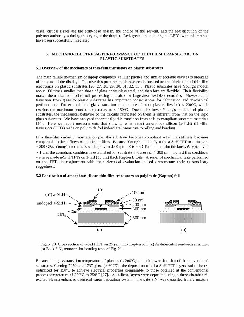
5.1 Overview of the mechanics of thin-film transistors on plastic substrates The main failure mechanism of laptop computers, cellular phones and similar portable devices is breakage of the glass of the display. To solve this problem much research is focused on the fabrication of thin-film electronics on plastic substrates [26, 27, 28, 29, 30, 31, 32, 33]. Plastic substrates have Young's moduli about 100 times smaller than those of glass or stainless steel, and therefore are flexible. Their flexibility makes them ideal for roll-to-roll processing and also for large-area flexible electronics. However, the transition from glass to plastic substrates has important consequences for fabrication and mechanical performance. For example, the glass transition temperature of most plastics lies below 200ºC, which restricts the maximum process temperature to ≤ 150ºC. Due to the lower Young's modulus of plastic substrates, the mechanical behavior of the circuits fabricated on them is different from that on the rigid glass substrates. We have analyzed theoretically this transition from stiff to compliant substrate materials [34]. Here we report measurements that show to what extent amorphous silicon (a-Si:H) thin-film transistors (TFTs) made on polyimide foil indeed are insensitive to rolling and bending. In a thin-film circuit / substrate couple, the substrate becomes compliant when its stiffness becomes comparable to the stiffness of the circuit films. Because Young's moduli Yf of the a-Si:H TFT materials are ~ 200 GPa, Young's modulus Ys of the polyimide Kapton E is ~ 5 GPa, and the film thickness df typically is ~ 1 µm, the compliant condition is established for substrate thickness ds << 300 µm. To test this condition, we have made a-Si:H TFTs on 1-mil (25 µm) thick Kapton E foils. A series of mechanical tests performed on the TFTs in conjunction with their electrical evaluation indeed demonstrate their extraordinary ruggedness. 5.2 Fabrication of amorphous silicon thin-film transistors on polyimide (Kapton) foil
Because the glass transition temperature of plastics (≤ 200ºC) is much lower than that of the conventional substrates, Corning 7059 and 1737 glass (≥ 600ºC), the deposition of all a-Si:H TFT layers had to be re-optimized for 150ºC to achieve electrical properties comparable to those obtained at the conventional process temperature of 250ºC to 350ºC [27]. All silicon layers were deposited using a three-chamber rf-excited plasma enhanced chemical vapor deposition system. The gate SiNx was deposited from a mixture
Cr (n + ) a- Si :H
undoped a- Si :H
SiN x Polyimide foil
100 nm
50 nm ~ 200 nm
360 nm
500 nm
(a)
Polyimide foil
(b)
Figure 20. Cross section of a-Si:H TFT on 25 µm thick Kapton foil. (a) As-fabricated sandwich structure. (b) Back SiNx removed for bending tests of Fig. 21.
of SiH4, NH3 and H2, the undoped a-Si:H from a mixture of SiH4 and H2, and the (n+) a-Si:H from a mixture of SiH4, PH3 and H2.
The TFTs have the bottom gate, back-channel etch structure shown in Fig. 20. We began by passivating a 25-µm-thick Kapton E substrate on both sides with 0.5 µm thick layers of SiNx. These layers serve as a barrier against the solvents, bases and acids used during photolithography. An ~ 100 nm thick Cr layer was thermally evaporated and wet etched to create the gate electrode. The TFT sequence was 360 nm of SiNx, ~ 200 nm of undoped a-Si:H, and ~ 50 nm of (n+) a-Si:H. An ~ 100 nm thick Cr layer was thermally evaporated. We wet etched the Cr source-drain pattern and dry etched the (n+) a-Si:H in CF4 gas. Then the undoped a-Si:H was dry etched to define the transistor island. In the last photolithographic step, we dry etched windows into the SiNx to open access to the gate contact pads. Arrays of TFTs with gate length L = 15 µm and width W = 210 µm were fabricated on 1.5 x 1.5 sq. in. substrates. Four substrates were processed simultaneously.
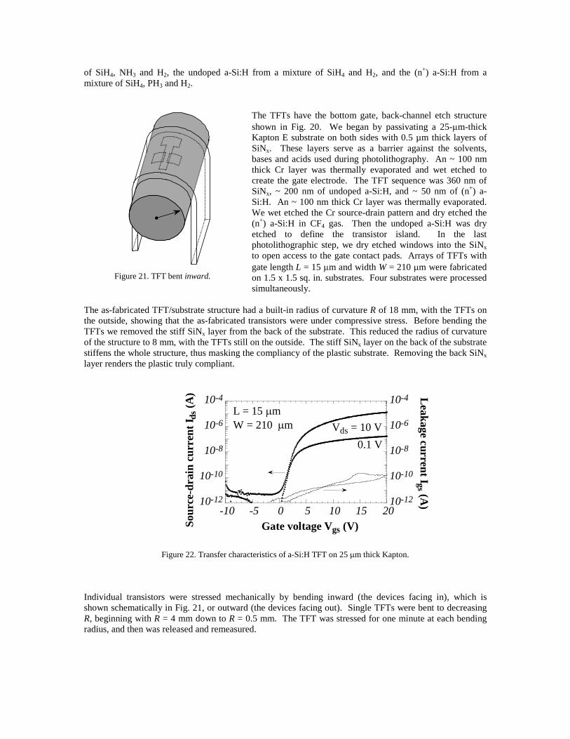
The as-fabricated TFT/substrate structure had a built-in radius of curvature R of 18 mm, with the TFTs on the outside, showing that the as-fabricated transistors were under compressive stress. Before bending the TFTs we removed the stiff SiNx layer from the back of the substrate. This reduced the radius of curvature of the structure to 8 mm, with the TFTs still on the outside. The stiff SiNx layer on the back of the substrate stiffens the whole structure, thus masking the compliancy of the plastic substrate. Removing the back SiNx layer renders the plastic truly compliant.
10-12
10-10
10-8
10-6
10-4
10-12
10-10
10-8
10-6
10-4
-10 -5 0 5 10 15 20
Sour
ce-d
rain
cur
rent
I ds (
A) Leakage current Igs (A
)
Gate voltage Vgs (V)
L = 15 µmW = 210 µm Vds = 10 V
0.1 V
Figure 22. Transfer characteristics of a-Si:H TFT on 25 µm thick Kapton.
Individual transistors were stressed mechanically by bending inward (the devices facing in), which is shown schematically in Fig. 21, or outward (the devices facing out). Single TFTs were bent to decreasing R, beginning with R = 4 mm down to R = 0.5 mm. The TFT was stressed for one minute at each bending radius, and then was released and remeasured.
S D
G
R R
Figure 21. TFT bent inward.
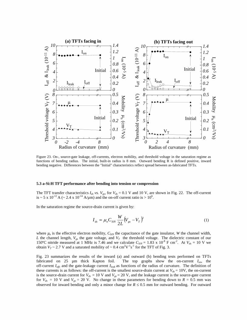
Figure 23. On-, source-gate leakage, off-currents, electron mobility, and threshold voltage in the saturation regime as functions of bending radius. The initial, built-in radius is 8 mm. Outward bending R is defined positive, inward bending negative. Differences between the "Initial" characteristics reflect spread between as-fabricated TFTs. 5.3 a-Si:H TFT performance after bending into tension or compression The TFT transfer characteristics Ids vs. Vgs, for Vds = 0.1 V and 10 V, are shown in Fig. 22. The off-current is ~ 5 x 10-12 A (~ 2.4 x 10⁻¹⁴ A/µm) and the on-off current ratio is > 106. In the saturation regime the source-drain current is given by:
( )22 TgsSiNnds VV
LWCI −= µ (1)
where µn is the effective electron mobility, CSiN the capacitance of the gate insulator, W the channel width, L the channel length, Vgs the gate voltage, and VT the threshold voltage. The dielectric constant of our 150ºC nitride measured at 1 MHz is 7.46 and we calculate CSiN = 1.83 x 10⁻⁸ F cm-2. At Vds = 10 V we obtain VT ~ 2.7 V and a saturated mobility of ~ 0.4 cm2V-1s-1 for the TFT of Fig. 3. Fig. 23 summarizes the results of the inward (a) and outward (b) bending tests performed on TFTs fabricated on 25 µm thick Kapton foil. The top graphs show the on-current Ion, the off-current Ioff, and the gate-leakage current Ileak as functions of the radius of curvature. The definition of these currents is as follows: the off-current is the smallest source-drain current at Vds = 10V, the on-current is the source-drain current for Vds = 10 V and Vgs = 20 V, and the leakage current is the source-gate current for Vds = 10 V and Vgs = 20 V. No change in these parameters for bending down to R = 0.5 mm was observed for inward bending and only a minor change for R ≤ 0.5 mm for outward bending. For outward
0 0
2
4
6
8
10
0.20.40.60.811.21.4
I off
& I
leak
(10-
11 A
)
Ion (10-5 A
)
Initial
Ion
Ileak Ioff
(a) TFTs facing in
3
4
5
6
7
8
0
0.1
0.2
0.3
0.4
0.5
0 -2 -4 8Thre
shol
d vo
ltage
VT
(V) M
obility µ
n (cm2/V
s)
Radius of curvature (mm)
InitialVT
µ
0
2
4
6
8
10
00.20.40.60.811.21.4
Ion (10-5 A
)
I off
& I
leak
(10-
11 A
)
Initial
Ion
Ileak Ioff
3
4
5
6
7
8
0
0.1
0.2
0.3
0.4
0.5
0 2 4 8Thre
shol
d vo
ltage
VT
(V) M
obility µ
n (cm2/V
s)
Radius of curvature (mm)
Initial
µ
VT
(b) TFTs facing out
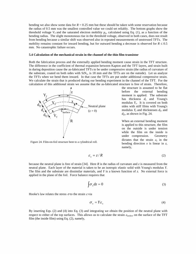
bending we also show some data for R = 0.25 mm but these should be taken with some reservation because the radius of 0.5 mm was the smallest controlled value we could set reliably. The bottom graphs show the threshold voltage VT and the saturated electron mobility µn, calculated using Eq. (1), as a function of the bending radius. The slight monotonous rise in the threshold voltage, observed in both cases, does not result from bending because a similar shift was observed also in repeated measurements of unstressed TFTs. The mobility remains constant for inward bending, but for outward bending a decrease is observed for R ≤ 0.5 mm. No catastrophic failure occurs. 5.4 Calculation of the mechanical strain in the channel of the thin film transistor Both the fabrication process and the externally applied bending moment cause strain in the TFT structure. The difference in the coefficient of thermal expansion between Kapton and the TFT layers, and strain built in during deposition cause the as-fabricated TFTs to be under compressive strain (the radius of curvature of the substrate, coated on both sides with SiNx, is 18 mm and the TFTs are on the outside). Let us analyze the TFTs when we bend them inward. In that case the TFTs are put under additional compressive strain. We calculate the strain that is produced during our bending experiment in the channel of the TFT. For the calculation of this additional strain we assume that the as-fabricated structure is free of strain. Therefore,
the structure is assumed to be flat before the external bending moment is applied. The substrate has thickness ds and Young's modulus Ys. It is covered on both sides with stiff films with Young's modulus Yf and thicknesses df1 and df2, as shown in Fig. 24. When an external bending moment is applied to this structure, the film on the outside is under tension while the film on the inside is under compression. Geometry dictates that the strain εx in the bending direction x is linear in z, namely,
Rzx /=ε (2)
because the neutral plane is free of strain [34]. Here R is the radius of curvature and z is measured from the neutral plane. Each layer of the material is taken to be an isotropic elastic solid with Young's modulus Y. The film and the substrate are dissimilar materials, and Y is a known function of z. No external force is applied in the plane of the foil. Force balance requires that
0=∫ dzxσ (3)
Hooke's law relates the stress σ to the strain ε via xx Yεσ = (4)
By inserting Eqs. (2) and (4) into Eq. (3) and integrating we obtain the position of the neutral plane with respect to either of the top surfaces. This allows us to calculate the strain εsurface on the surface of the TFT film (the inside film) using Eq. (2), namely,
d s
d f1
d f2 Y f
Y s
Y f
ε surface
Neutral plane (z = 0)
R
z
Figure 24. Film-on-foil structure bent to a cylindrical roll.
x
( ) ( )( ) ( )( ) 11
12.2 21
221
221122
2121
+++++
+++++++
=
χηηηηχ
ηηχηχηηηχε
Rddd ffs
surface (5)
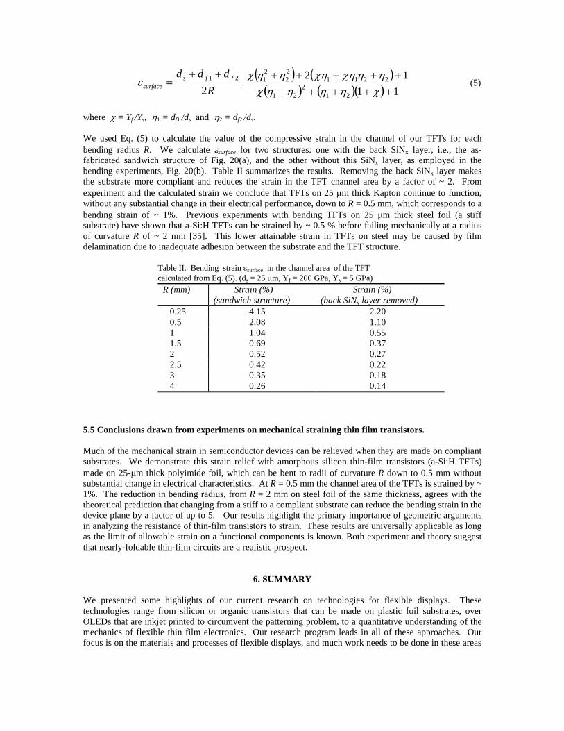
where χ = Yf /Ys, η1 = df1 /ds and η2 = df2 /ds. We used Eq. (5) to calculate the value of the compressive strain in the channel of our TFTs for each bending radius R. We calculate εsurface for two structures: one with the back SiNx layer, i.e., the as-fabricated sandwich structure of Fig. 20(a), and the other without this SiNx layer, as employed in the bending experiments, Fig. 20(b). Table II summarizes the results. Removing the back SiNx layer makes the substrate more compliant and reduces the strain in the TFT channel area by a factor of ~ 2. From experiment and the calculated strain we conclude that TFTs on 25 µm thick Kapton continue to function, without any substantial change in their electrical performance, down to R = 0.5 mm, which corresponds to a bending strain of ~ 1%. Previous experiments with bending TFTs on 25 µm thick steel foil (a stiff substrate) have shown that a-Si:H TFTs can be strained by ~ 0.5 % before failing mechanically at a radius of curvature R of ~ 2 mm [35]. This lower attainable strain in TFTs on steel may be caused by film delamination due to inadequate adhesion between the substrate and the TFT structure.
Table II. Bending strain εsurface in the channel area of the TFT calculated from Eq. (5). (ds = 25 µm, Yf = 200 GPa, Ys = 5 GPa)
R (mm) Strain (%) (sandwich structure)
Strain (%) (back SiNx layer removed)
0.25 4.15 2.20 0.5 2.08 1.10 1 1.04 0.55 1.5 0.69 0.37 2 0.52 0.27 2.5 0.42 0.22 3 0.35 0.18 4 0.26 0.14
5.5 Conclusions drawn from experiments on mechanical straining thin film transistors. Much of the mechanical strain in semiconductor devices can be relieved when they are made on compliant substrates. We demonstrate this strain relief with amorphous silicon thin-film transistors (a-Si:H TFTs) made on 25-µm thick polyimide foil, which can be bent to radii of curvature R down to 0.5 mm without substantial change in electrical characteristics. At R = 0.5 mm the channel area of the TFTs is strained by ~ 1%. The reduction in bending radius, from R = 2 mm on steel foil of the same thickness, agrees with the theoretical prediction that changing from a stiff to a compliant substrate can reduce the bending strain in the device plane by a factor of up to 5. Our results highlight the primary importance of geometric arguments in analyzing the resistance of thin-film transistors to strain. These results are universally applicable as long as the limit of allowable strain on a functional components is known. Both experiment and theory suggest that nearly-foldable thin-film circuits are a realistic prospect.
6. SUMMARY We presented some highlights of our current research on technologies for flexible displays. These technologies range from silicon or organic transistors that can be made on plastic foil substrates, over OLEDs that are inkjet printed to circumvent the patterning problem, to a quantitative understanding of the mechanics of flexible thin film electronics. Our research program leads in all of these approaches. Our focus is on the materials and processes of flexible displays, and much work needs to be done in these areas
to create a manufacturable technology. The rate of progress that we have been experiencing in our collaborative program instills optimism. We are certain that flexible displays are in our future.
ACKNOWLEDGEMENTS
We want to express our appreciation to our collaborators, Sanghoon Bae, David Gundlach, Jiunn-Ru Huang, Lili Jia, Chung-Chen Kuo, Lisong Zhou, Jon Nichols, Conor Madigan, Helena Gleskova and Zhigang Suo. The support of this work by DARPA's High Definition Systems Program, and its management by the Air Force Research Laboratory, are gratefully acknowledged. Part of this work is supported by the Navy through the Naval Surface Warfare Center, Dahlgren Division. The Penn State Nanofabrication facility is supported by NSF. TNJ acknowledges a productive collaboration with the Sarnoff Corporation, and JCS and SW with Printed Transistor, Inc.
REFERENCES
1. John L. Crowley, Osama O. Awadelkarim, Stephen J. Fonash, Tom Jackson, Antoine Kahn, Terry Peterson, James C. Sturm and Sigurd Wagner, Industry/University Teaming for Display Research, SPIE Technical Conference, Orlando 3057, 60-67 (1997). 2. S.J. Fonash, O. Awadelkarim, J.L. Crowley, T.N. Jackson, A. Kahn, J.C. Sturm and S. Wagner, Device technology for lightweight panoramic displays, Cockpit Display IV: Flat Panel Display for Defense Applications, Proc. of SPIE 3057, 570-580 (1997). 3. A. Krishnan, S. Bae, and S. Fonash, Solid State Electronics 44, 1163 (2000). 4. S. Bae, D. Farber, and S. Fonash, Electrochemical and Solid-State Letters 3, 41 (2000). 5. S. Bae and S. Fonash, Journal of Vacuum Sciences and Technology A 17, 1987 (1999). 6. A. Kaan, S. Bae, H. Li, and S. Fonash, Journal of Applied Physics 88, 555 (2000). 7. A. Dodabalapur, Z. Bao, A. Makhija, J. G. Laquindanum, V. R. Raju, Y. Feng, H. E. Katz, and J. Rogers, “Organic Smart Pixels,” Appl. Phys. Lett. 73, pp. 142-144, July 1998. 8. H. Klauk, B. D'Andrade, and T. N. Jackson, “All-Organic Integrated Emissive Pixels,” 57th Annual Device Research Conference Digest, pp. 162-163, June 1999 9. M. Hack, J. J. Brown, J. K. Mahon, R. Kwong, and R. Hewitt, “Performance of High Efficiency AMOLED Displays,” IDMC, Seoul, Korea, September 2000. 10. J. H. Schon, S. Berg, Ch. Klock, and B. Batlogg, “Ambipolar Pentacene Field-Effect Transistors and Inverters,” Science 287, pp. 1022-1023, February 2000. 11. D. J. Gundlach, H. Klauk, C. D. Sheraw, C.-C. Kuo, J.-R. Huang, and T. N. Jackson, “High-Mobility, Low Voltage Organic Thin Film Transistors,” 1999 International Electron Devices Meeting Technical Digest, pp. 249-252, December 1999. 12. J. G. Laquindanum, H. E. Katz, A. J. Lovinger, and A. Dodabalapur, “Morphological Origin of High Mobility in Pentacene Thin-Film Transistors,” Chem. Mater. 8, pp. 2542-2544, 1996. 13. H. Klauk, D. J. Gundlach, J. A. Nichols, and T. N. Jackson, “Pentacene Organic Thin-Film Transistors for Circuit and Display Applications,” IEEE Trans. Electron Devices 46, pp. 1258-1263, June 1999. 14. J.H. Burroughs et al., Nature 347, 539 (1990). 15. T.R. Hebner, C.C. Wu, D. Marcy, M.H. Lu, and J.C. Sturm, Appl. Phys. Lett. 72, 519 (1998). 16. J. Bharathan and Y. Yang, Appl. Phys. Lett. 72, 2660 (1998). 17. T. Shimoda, M. Kimura, S. Seki, et al, Tech. Dig. Int. Elec.Dev. Mtg., 107 (1999). 18. J.C. Sturm, T.R. Hebner, C.C. Wu, D. Marcy, M.H. Lu, and J.C. Sturm, U.S. Patent 6,087,196 (2000). 19. E.D. Wilkes et al., Phys. of Fluids, 11, 3577 (1999). 20. X.G. Zhang, J. Coll. Int. Sci., 212, 107 (1999). 21. T.W. Shield et al., IBM J. Res. Dev., 31, 96 (1987). 22. T.R. Hebner and J.C. Sturm, Appl. Phys. Lett. 73, 1775 (1998). 23. S.C. Chang, J. Bharathan, Y. Yang, R. Gelgeson, F. Wudl, M.B. Ramey and J.R. Reynolds, Appl. Phys. Lett. 73, 2561 (1998). 24. C. Madigan, T.R. Hebner, J.C. Sturm, R.A. Register and S. Troian, Proc. Symp. Mat. Res. Soc. 624 (April, 2000).
25. C.-C. Wu, J.C. Sturm, R.A. Register, J. Tian, L. Dana and M.E. Thompson, IEEE Trans. On Elec. Dev. 44, 1269 (1997). 26. G.N. Parsons, C.S. Yang, C.B. Arthur, T.M. Klein, and L. Smith, in Flat Panel Display Materials 1998, edited by G.N. Parsons, C.C. Tsai, T.S. Fahlen, and C.H. Seager, (Mat. Res. Soc. Symp. Proc. 508, Pittsburgh, PA, 1998), pp. 19-24. 27. H. Gleskova, S. Wagner and Z. Suo, in Flat Panel Display Materials - 1998, edited by G.N. Parsons, C.C. Tsai, T.S. Fahlen, and C.H. Seager, (Mat. Res. Soc. Symp. Proc. 508, Pittsburgh, PA, 1998), pp. 73-78. 28. J.N. Sandoe, Digest of Technical Papers of the Society for Information Display, Vol. 29, 1998, pp. 293-296. 29. E. Lueder, M. Muecke, S. Polach, Proc. of the Int. Display Research Conf., Asia Display '98, 1998, pp. 173-177. 30. A. Constant, S.G. Burns, H. Shanks, C. Gruber, A. Landin, D. Schmidt, C. Thielen, F. Olympie, T. Schumacher, and J. Cobbs, The Electrochemical Society Proceedings, Vol. 94-35, pp. 392-400. 31. S.G. Burns, H. Shanks, A. Constant, C. Gruber, D. Schmidt, A. Landin, and F. Olympie, The Electrochemical Society Proceedings, Vol. 96-23, pp. 382-390. 32. S. D. Theiss, P. G. Carey, P.M. Smith, P. Wickboldt, T.W. Sigmon, Y.J. Tung, and T.-J. King, IEEE Int. Electron Devices Meeting 1998, Technical Digest, pp. 257-260. 33. D.B. Thomasson, M. Bonse, J.R. Huang, C.R. Wronski, and T.N. Jackson, IEEE Int. Electron Devices Meeting 1998, Technical Digest, pp. 253-256. 34. Z. Suo, E.Y. Ma, H. Gleskova, and S. Wagner, Appl. Phys. Lett. 74, 1999, pp. 1177-1179. 35 E.Y. Ma and S. Wagner, in Flat Panel Display Materials - 1998, edited by G.N. Parsons, C.C. Tsai, T.S. Fahlen, and C.H. Seager, (Mat. Res. Soc. Symp. Proc. 508, Pittsburgh, PA, 1998), pp. 13-18.