flexible electronics materials display products core tft-lcd equipment new equipment segments cvd...
TRANSCRIPT
External Use
Flexible Electronics
Near-Term and Future Opportunities
IESA CXO Conclave
Om Nalamasu, PhD
CTO, Applied Materials
President, Applied Ventures, LLC
March 22nd 2016
External Use2
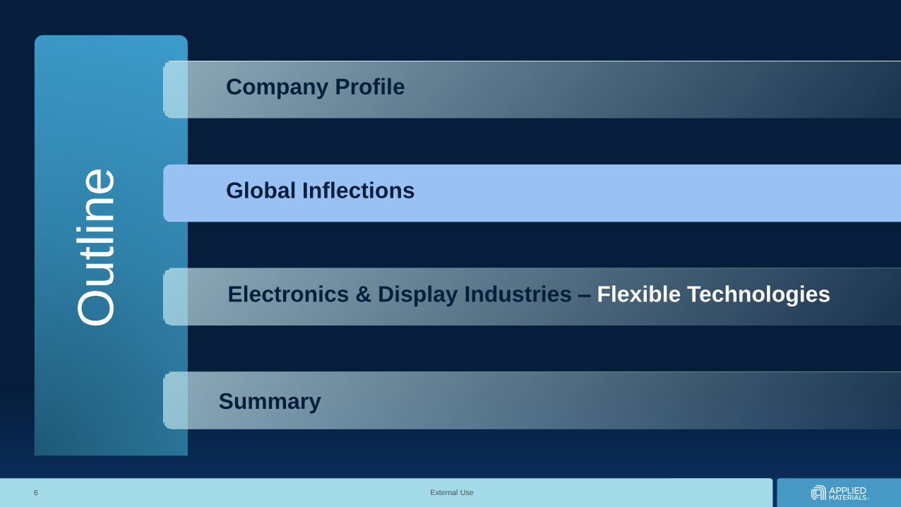
Company Profile
Electronics & Display Industries – Flexible Technologies
Global Inflections
Ou
tlin
e
External Use
Summary
External Use
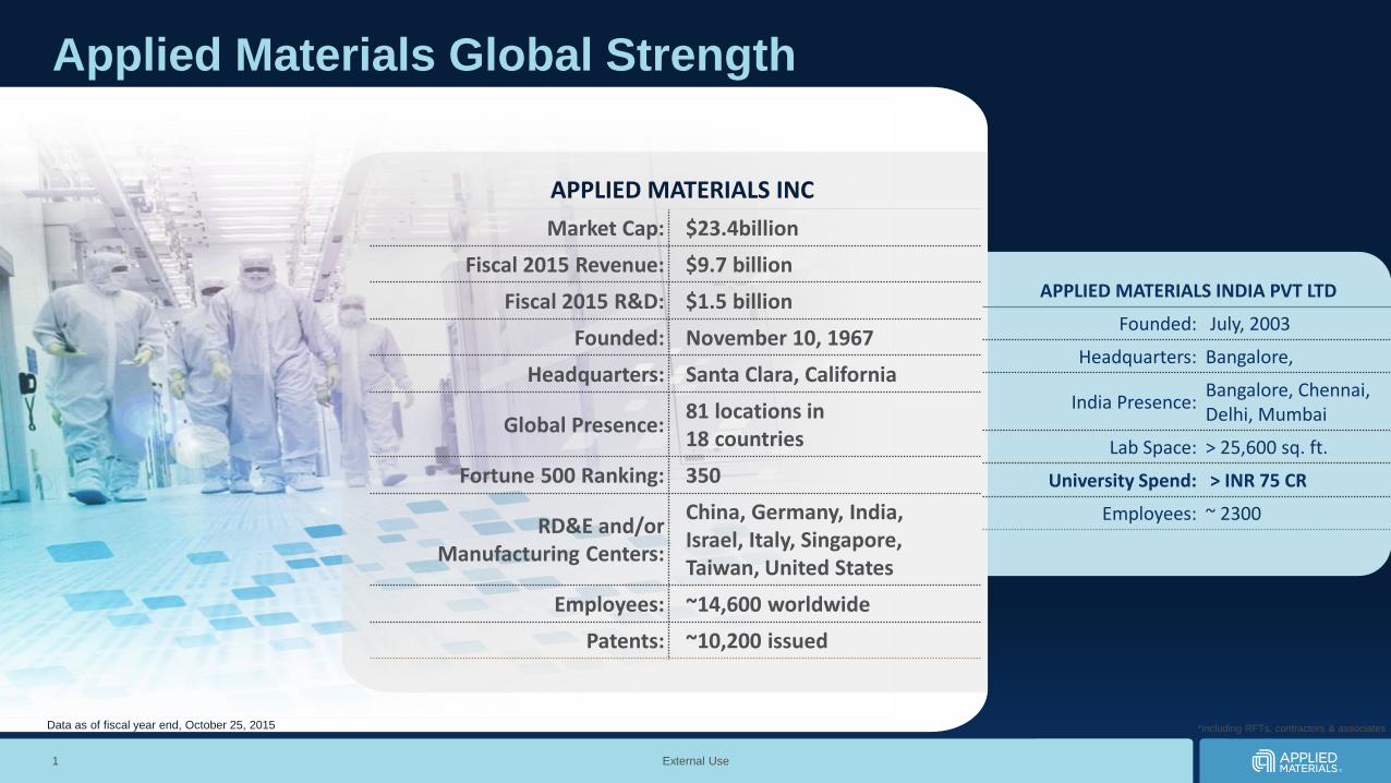
APPLIED MATERIALS INC
Market Cap: $23.4billion
Fiscal 2015 Revenue: $9.7 billion
Fiscal 2015 R&D: $1.5 billion
Founded: November 10, 1967
Headquarters: Santa Clara, California
Global Presence:81 locations in 18 countries
Fortune 500 Ranking: 350
RD&E and/or Manufacturing Centers:
China, Germany, India, Israel, Italy, Singapore, Taiwan, United States
Employees: ~14,600 worldwide
Patents: ~10,200 issued
*Including RFTs, contractors & associates
APPLIED MATERIALS INDIA PVT LTD
Founded: July, 2003
Headquarters: Bangalore,
India Presence:Bangalore, Chennai, Delhi, Mumbai
Lab Space: > 25,600 sq. ft.
University Spend: > INR 75 CR
Employees: ~ 2300
Applied Materials Global Strength
1
Data as of fiscal year end, October 25, 2015
External Use
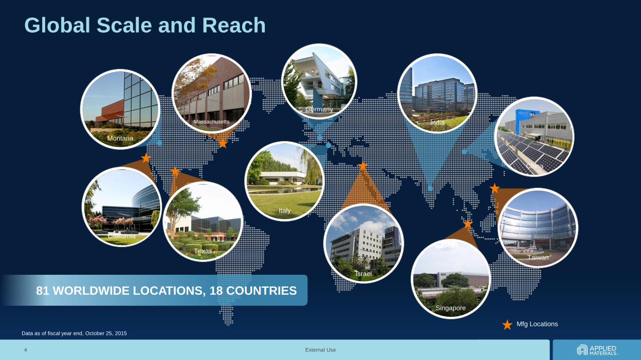
Global Scale and Reach
4
Taiwan
China
Italy
Singapore
Israel
California
Texas
Montana
Massachusetts India
81 WORLDWIDE LOCATIONS, 18 COUNTRIES
Mfg Locations
Data as of fiscal year end, October 25, 2015
Germany
External Use
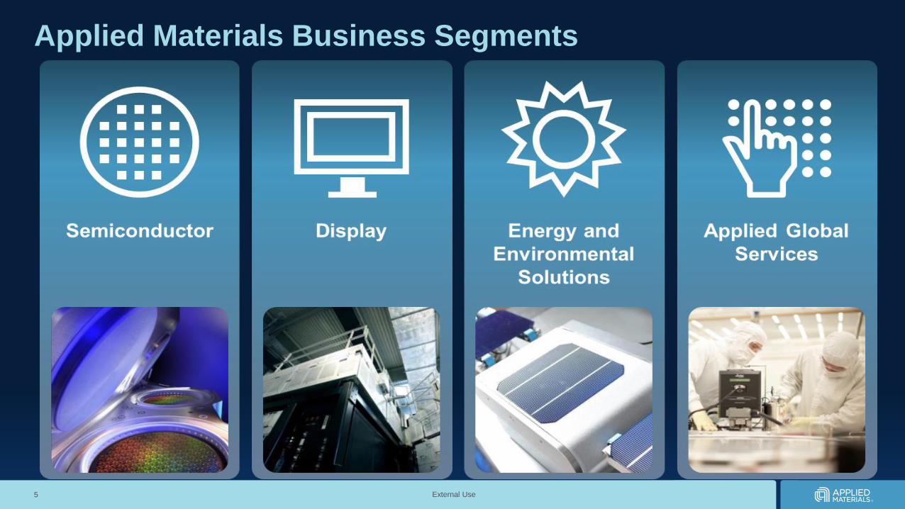
Applied Materials Business Segments
5 External Use
External Use6
Company Profile
Electronics & Display Industries – Flexible Technologies
Global Inflections
Ou
tlin
e
External Use
Summary
External Use
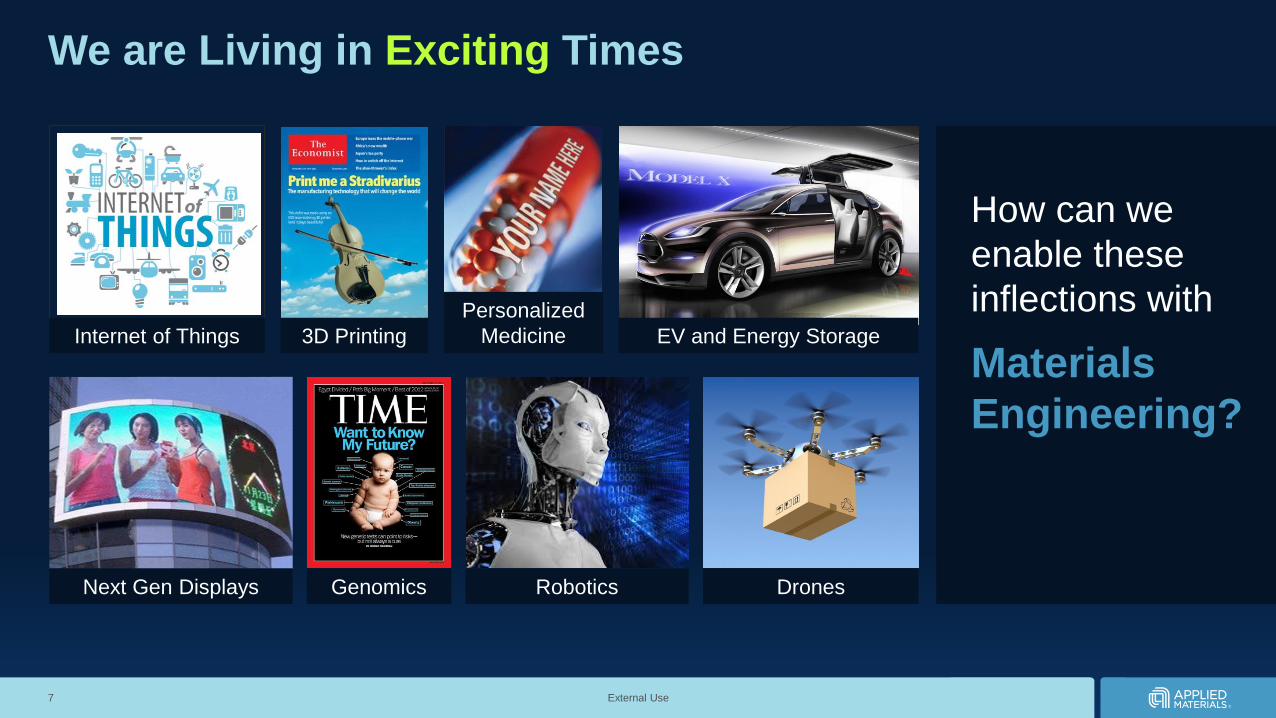
We are Living in Exciting Times
7
Next Gen Displays
3D Printing
Personalized
Medicine EV and Energy Storage
RoboticsGenomics Drones
How can we
enable these
inflections with
Materials
Engineering?
Internet of Things
External Use
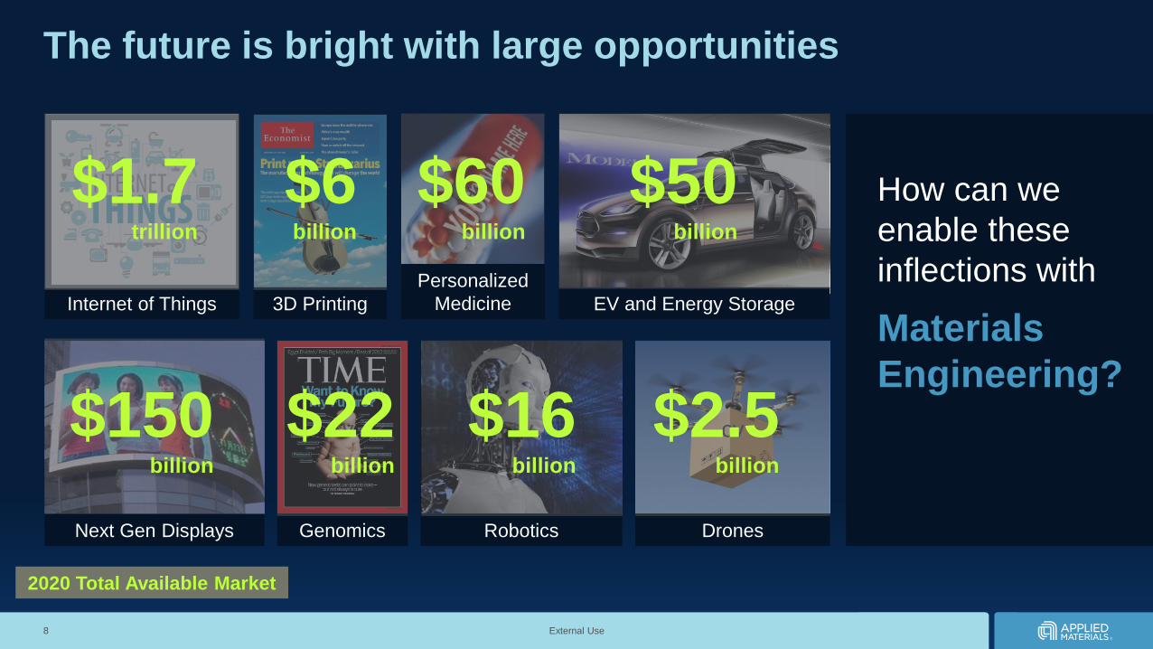
The future is bright with large opportunities
8
Next Gen Displays
3D Printing
Personalized
Medicine EV and Energy Storage
RoboticsGenomics Drones
How can we
enable these
inflections with
Materials
Engineering?
Internet of Things
cv$150billion
cvcv
cv
cv cvcv
$1.7trillion
$16billion
$2.5billion
$6billion
$50billion
$60billion
$22billion
2020 Total Available Market
External Use
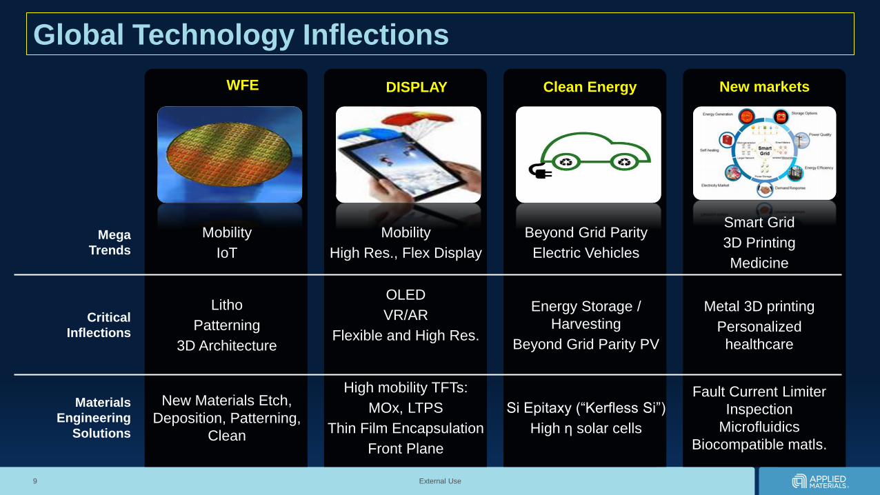
Global Technology Inflections
9
WFE DISPLAY Clean Energy New markets
Mega
Trends
Mobility
IoT
Mobility
High Res., Flex Display
Beyond Grid Parity
Electric Vehicles
Smart Grid
3D Printing
Medicine
Critical
Inflections
Litho
Patterning
3D Architecture
OLED
VR/AR
Flexible and High Res.
Energy Storage /
Harvesting
Beyond Grid Parity PV
Metal 3D printing
Personalized
healthcare
Materials
Engineering
Solutions
New Materials Etch,
Deposition, Patterning,
Clean
High mobility TFTs:
MOx, LTPS
Thin Film Encapsulation
Front Plane
Si Epitaxy (“Kerfless Si”)
High η solar cells
Fault Current Limiter
Inspection
Microfluidics
Biocompatible matls.
External Use
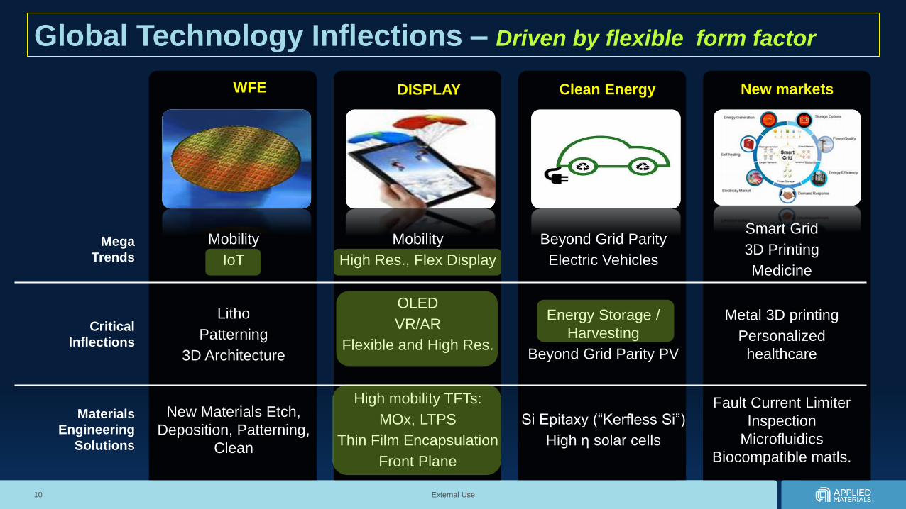
Global Technology Inflections – Driven by flexible form factor
10
WFE DISPLAY Clean Energy New markets
Mega
Trends
Mobility
IoT
Mobility
High Res., Flex Display
Beyond Grid Parity
Electric Vehicles
Smart Grid
3D Printing
Medicine
Critical
Inflections
Litho
Patterning
3D Architecture
OLED
VR/AR
Flexible and High Res.
Energy Storage /
Harvesting
Beyond Grid Parity PV
Metal 3D printing
Personalized
healthcare
Materials
Engineering
Solutions
New Materials Etch,
Deposition, Patterning,
Clean
High mobility TFTs:
MOx, LTPS
Thin Film Encapsulation
Front Plane
Si Epitaxy (“Kerfless Si”)
High η solar cells
Fault Current Limiter
Inspection
Microfluidics
Biocompatible matls.
External Use
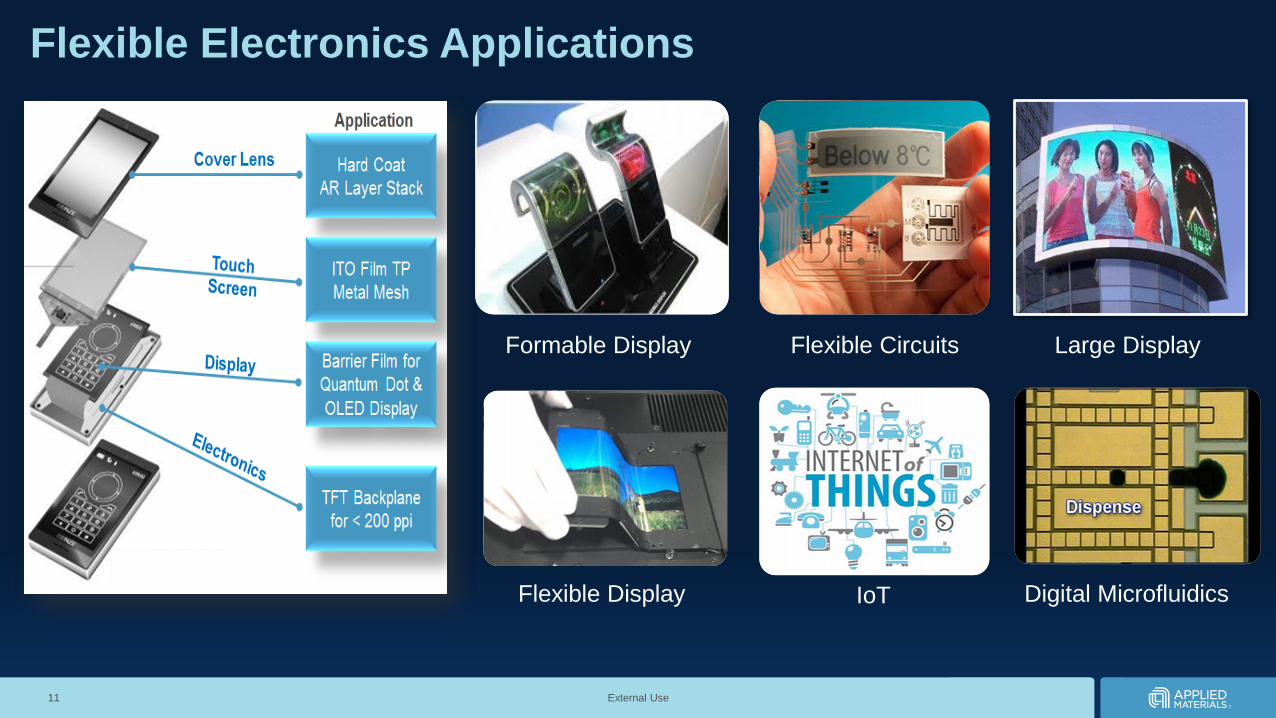
Flexible Electronics Applications
11
Digital Microfluidics
Formable Display
Flexible Display IoT
Flexible Circuits Large Display
External Use12
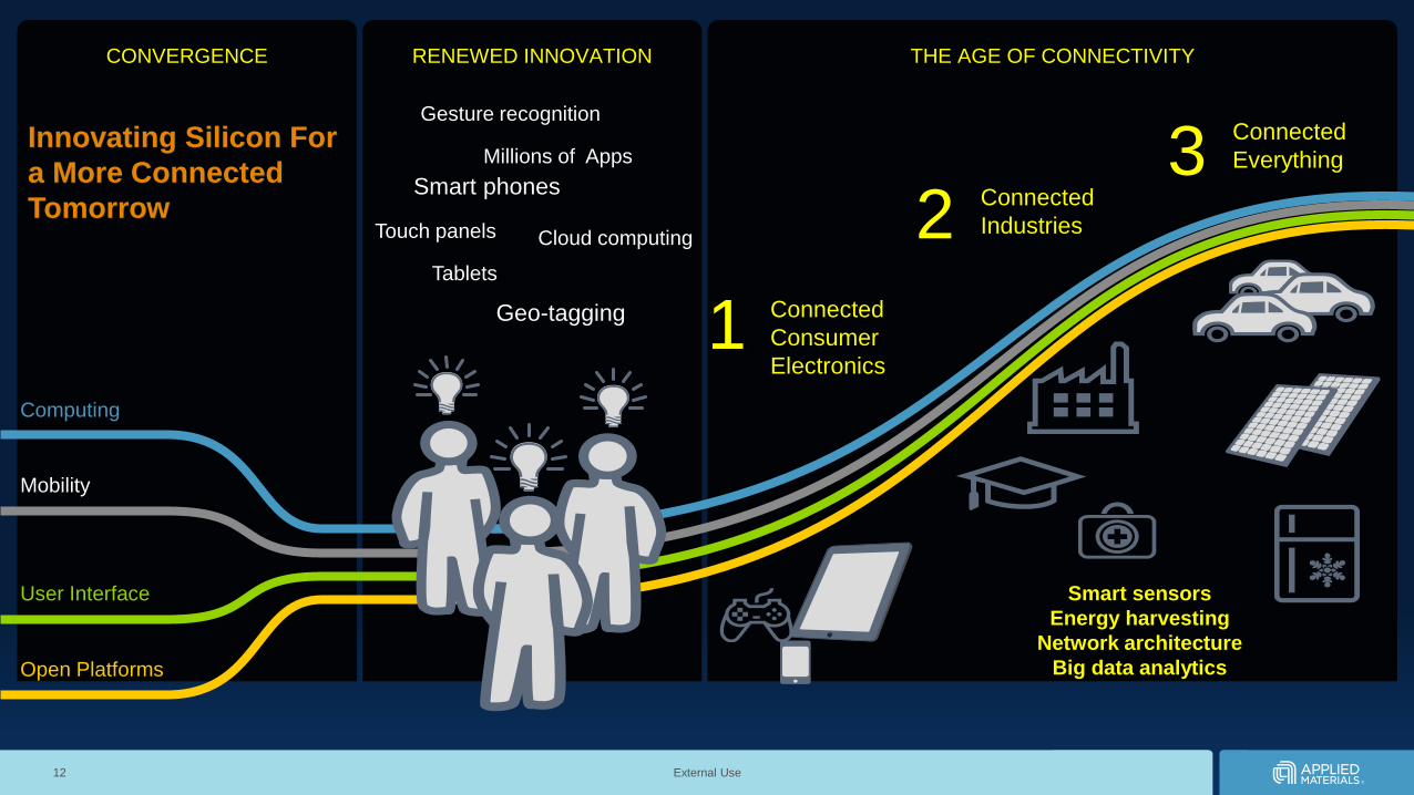
RENEWED INNOVATION THE AGE OF CONNECTIVITYCONVERGENCE
Computing
Mobility
User Interface
Open Platforms
Connected
Consumer
Electronics1
Connected
Industries2
Connected
Everything3
Geo-tagging
Gesture recognition
Touch panels Cloud computing
Millions of Apps
Tablets
Smart phones
Innovating Silicon For
a More Connected
Tomorrow
Smart sensors
Energy harvesting
Network architecture
Big data analytics
External Use
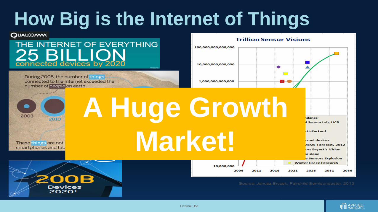
How Big is the Internet of Things
A Huge Growth
Market!
External Use14
Company Profile
Electronics & Display Industries – Flexible Technologies
Global Inflections
Ou
tlin
e
External Use
Summary
External Use
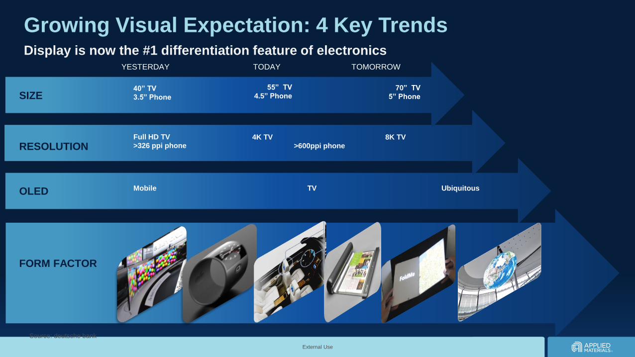
Growing Visual Expectation: 4 Key TrendsDisplay is now the #1 differentiation feature of electronics
4K TV 8K TV
>600ppi phone
Full HD TV
>326 ppi phone
70” TV
5” Phone40” TV
3.5” Phone
Mobile TV Ubiquitous
55” TV
4.5” PhoneSIZE
RESOLUTION
OLED
FORM FACTOR
TODAYYESTERDAY TOMORROW
Source: deutsche bank
External Use
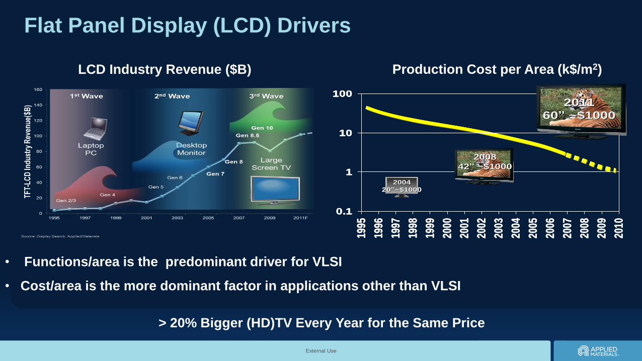
Flat Panel Display (LCD) Drivers
> 20% Bigger (HD)TV Every Year for the Same Price
LCD Industry Revenue ($B) Production Cost per Area (k$/m2)
0.1
1
10
100
1995
1996
1997
1998
1999
2000
2001
2002
2003
2004
2005
2006
2007
2008
2009
2010
20042004
2020””~$1000~$100020042004
2020””~$1000~$1000
20082008
4242”” ~$1000~$100020082008
4242”” ~$1000~$1000
2011 2011
6060”” ~$1000~$10002011 2011
6060”” ~$1000~$1000
0.1
1
10
100
1995
1996
1997
1998
1999
2000
2001
2002
2003
2004
2005
2006
2007
2008
2009
2010
20042004
2020””~$1000~$100020042004
2020””~$1000~$1000
20082008
4242”” ~$1000~$100020082008
4242”” ~$1000~$1000
2011 2011
6060”” ~$1000~$10002011 2011
6060”” ~$1000~$1000
0.1
1
10
100
1995
1996
1997
1998
1999
2000
2001
2002
2003
2004
2005
2006
2007
2008
2009
2010
20042004
2020””~$1000~$100020042004
2020””~$1000~$1000
20082008
4242”” ~$1000~$100020082008
4242”” ~$1000~$1000
2011 2011
6060”” ~$1000~$10002011 2011
6060”” ~$1000~$1000
• Functions/area is the predominant driver for VLSI
• Cost/area is the more dominant factor in applications other than VLSI

External Use
Substrate Size Driving Costs Down
Mean time to double the substrate size = 1.5 years after Gen 4.5
Gen 10 = 60nm uniformity over ~ 1019 nm2 area at 50sph
2880x3130
4 up
10.4”6 up
12.1”
6 up
15” ~ 17”
6 up
19” ~ 24”
6 up
37” Wide panels6 up
52” Wide panels
6 up65” Wide panels
Panel size
Inch
10.4 12.1 15 ~ 17 21 ~ 24 46W37W32W 52W
Panel/sub 4 6 6 6 666 6
Application Note PC -----------------> Monitor TV----------------->
1/ '06~
ACLS
AKT 90K2850x3050 class
Gen 10
90,144cm2(1.63 from 55 K)
12/ '08~
57W / 65W
8 / 6
1600370x470
400x500
3500 / 4300 / 4300A
550x650
600x720
620x750
5500/5500A680x880
730x920
15K / 15KA1100x1250
1200x1300
Substrate
Area
2,000 cm2(1.00)
4,650 cm2(2.33 from 1600)
6,716 cm2(1.44 from 4300)
15,600 cm2(1.30 from 10K)
40K / 40KA1870x2200
1950x2250
41,140 cm2(1.52 from 25 K)
Model
Substrate
Size (mm)
Gen 2 Gen 3 / 3.5 Gen 4 Gen 5 Gen 7 / 7.5
System
Layout
ACLS ACLS
2/ '93~ 4/ '95~ 1/ '00~ 6/ '02~ 7/ '04~1st Release
ACLS
25K / 25KA1500x1800
1500x1850
27,750 cm2(1.78 from 15 K)
5/ '03~
Gen 6Gen 5.5
19,500 cm2(1.25 from 15 K)
20K1300x1500
ACLS
8/ '04~
Gen 8 / 8.5
ACLS
50K / 55K2160x2400 class
2200x2500
53,136 cm2(1.21 from 40 KA)
TFT-LCD TVDesktop MonitorNotebook PC
4 up
10.4”6 up
12.1”
6 up
15” ~ 17”
6 up
19” ~ 24”
6 up
37” Wide panels6 up
52” Wide panels
6 up65” Wide panels
4 up
10.4”6 up
12.1”
6 up
15” ~ 17”
6 up
19” ~ 24”
6 up
37” Wide panels6 up
52” Wide panels
4 up
10.4”
4 up
10.4”6 up
12.1”
6 up
12.1”
6 up
15” ~ 17”
6 up
15” ~ 17”
6 up
19” ~ 24”
6 up
19” ~ 24”
6 up
37” Wide panels
6 up
37” Wide panels6 up
52” Wide panels
6 up
52” Wide panels
6 up65” Wide panels
Panel size
Inch
10.4 12.1 15 ~ 17 21 ~ 24 46W37W32W 52W
Panel/sub 4 6 6 6 666 6
Application Note PC -----------------> Monitor TV----------------->
1/ '06~
ACLS
AKT 90K2850x3050 class
Gen 10
90,144cm2(1.63 from 55 K)
12/ '08~
57W / 65W
8 / 6
1600370x470
400x500
3500 / 4300 / 4300A
550x650
600x720
620x750
5500/5500A680x880
730x920
15K / 15KA1100x1250
1200x1300
Substrate
Area
2,000 cm2(1.00)
4,650 cm2(2.33 from 1600)
6,716 cm2(1.44 from 4300)
15,600 cm2(1.30 from 10K)
40K / 40KA1870x2200
1950x2250
41,140 cm2(1.52 from 25 K)
Model
Substrate
Size (mm)
Gen 2 Gen 3 / 3.5 Gen 4 Gen 5 Gen 7 / 7.5
System
Layout
ACLS ACLS
2/ '93~ 4/ '95~ 1/ '00~ 6/ '02~ 7/ '04~1st Release
ACLS
25K / 25KA1500x1800
1500x1850
27,750 cm2(1.78 from 15 K)
5/ '03~
Gen 6Gen 5.5
19,500 cm2(1.25 from 15 K)
20K1300x1500
ACLS
8/ '04~
Gen 8 / 8.5
ACLS
50K / 55K2160x2400 class
2200x2500
53,136 cm2(1.21 from 40 KA)
TFT-LCD TVDesktop MonitorNotebook PC
External Use
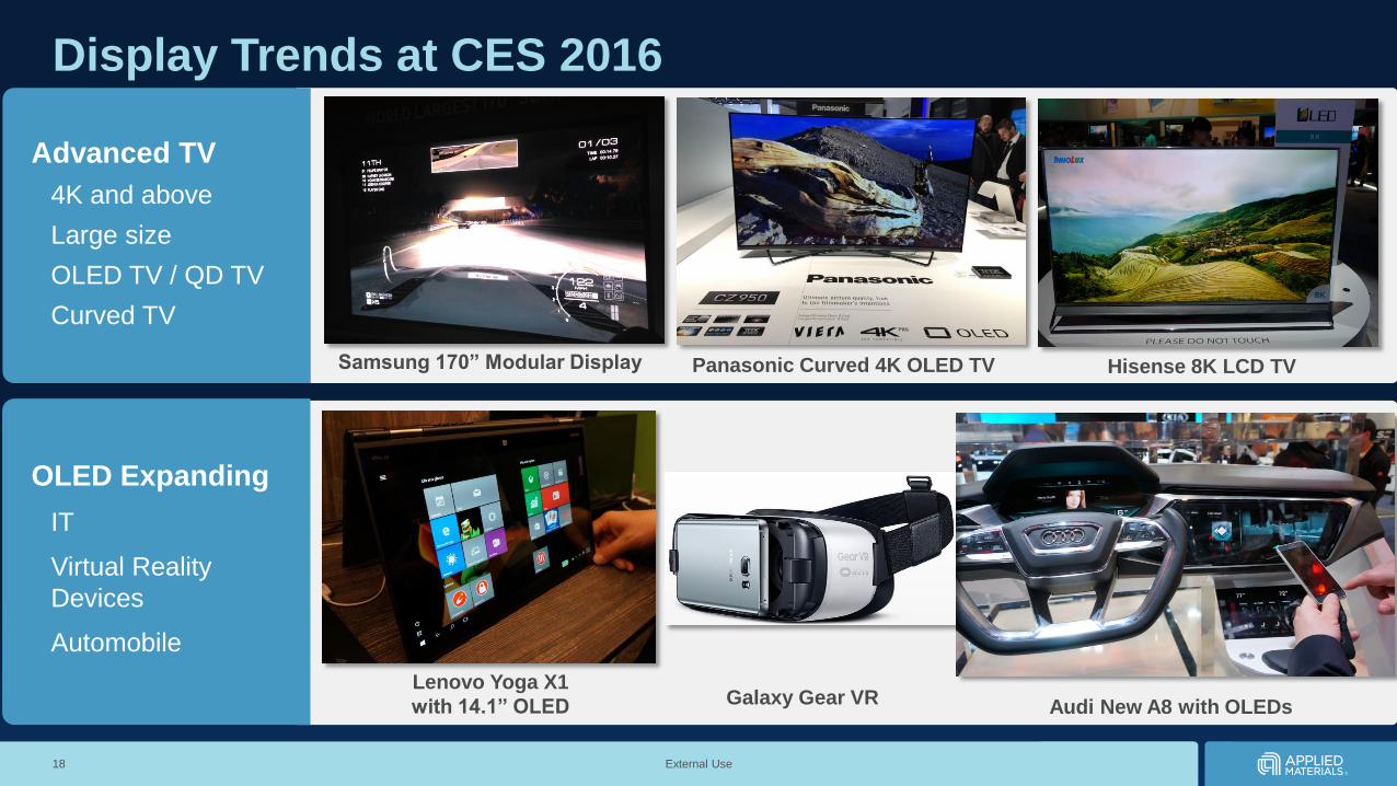
Display Trends at CES 2016
18
Advanced TV
4K and above
Large size
OLED TV / QD TV
Curved TV
OLED Expanding
IT
Virtual Reality
Devices
Automobile
Panasonic Curved 4K OLED TVSamsung 170” Modular Display Hisense 8K LCD TV
Audi New A8 with OLEDs
Lenovo Yoga X1
with 14.1” OLED Galaxy Gear VR
External Use
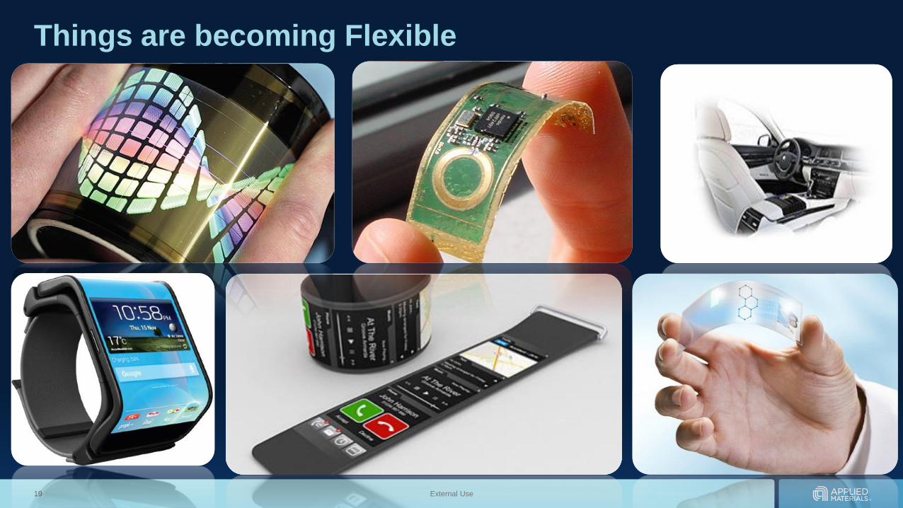
Things are becoming Flexible
19
External Use
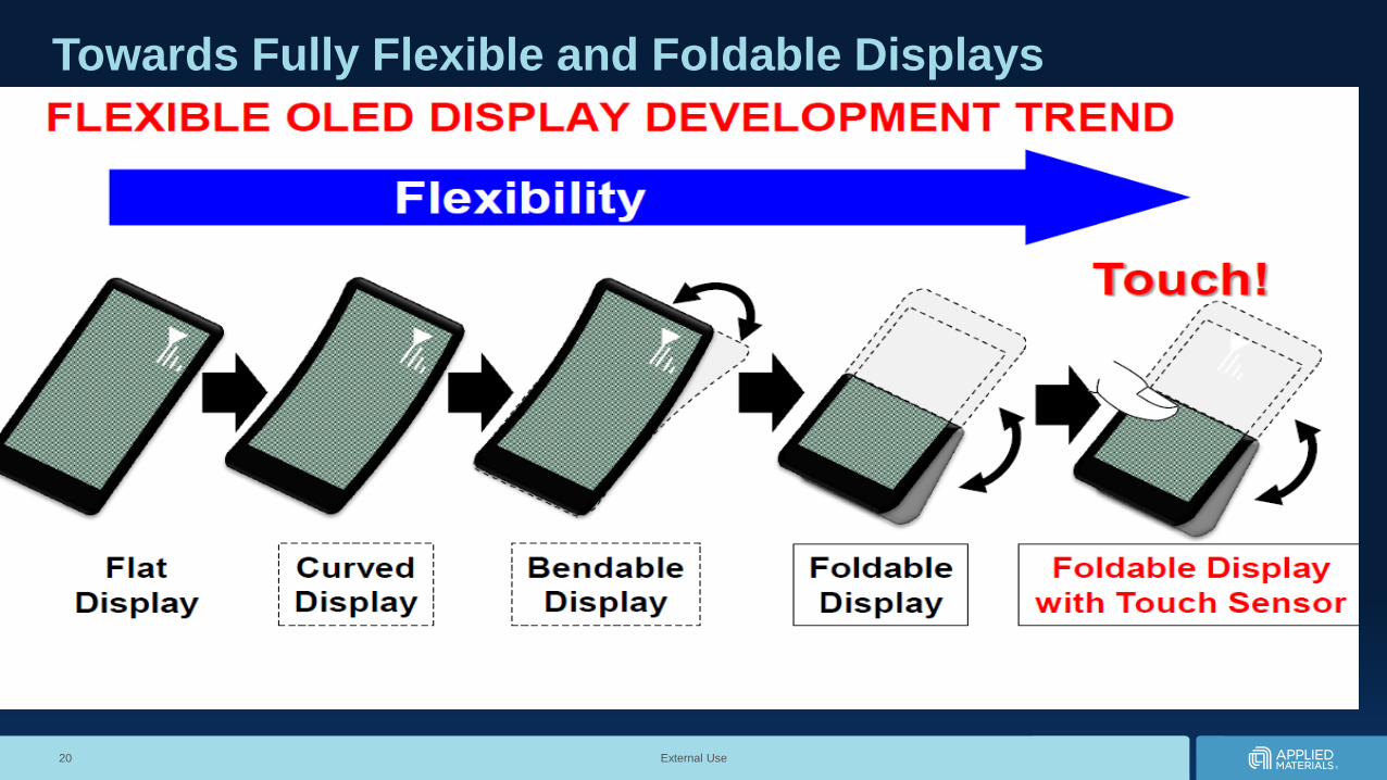
Towards Fully Flexible and Foldable Displays
20
External Use
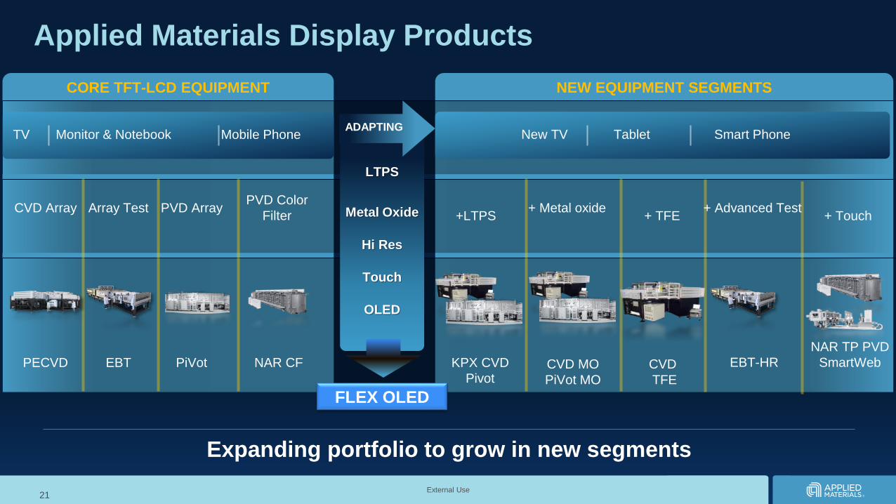
Applied Materials Display Products
NEW EQUIPMENT SEGMENTSCORE TFT-LCD EQUIPMENT
CVD Array Array Test PVD ArrayPVD Color
Filter
PECVD PiVot NAR CF
TV Monitor & Notebook Mobile Phone
+LTPS+ Metal oxide
+ Touch
New TV Tablet Smart Phone
CVD MO
PiVot MO
NAR TP PVD
SmartWeb
ADAPTING
LTPS
Metal Oxide
Hi Res
Touch
OLED
KPX CVD
Pivot
EBT
Expanding portfolio to grow in new segments
+ TFE
CVD
TFE
+ Advanced Test
EBT-HR
21
FLEX OLED
External Use
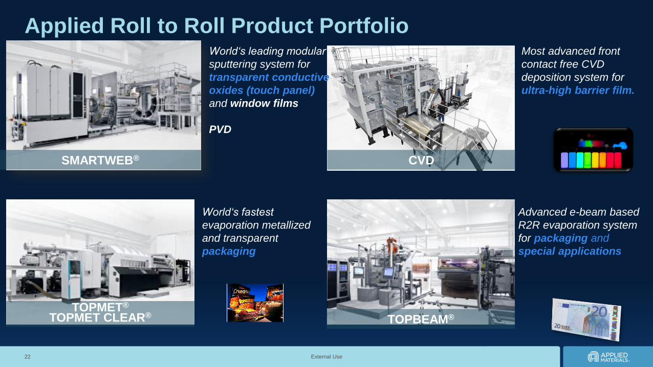
Applied Roll to Roll Product Portfolio
22
Advanced e-beam based
R2R evaporation system
for packaging and
special applications
TOPBEAM®
SMARTWEB®
TOPMET®
TOPMET CLEAR®
CVD
World‘s leading modular
sputtering system for
transparent conductive
oxides (touch panel)
and window films
PVD
World‘s fastest
evaporation metallized
and transparent
packaging
Most advanced front
contact free CVD
deposition system for
ultra-high barrier film.
External Use
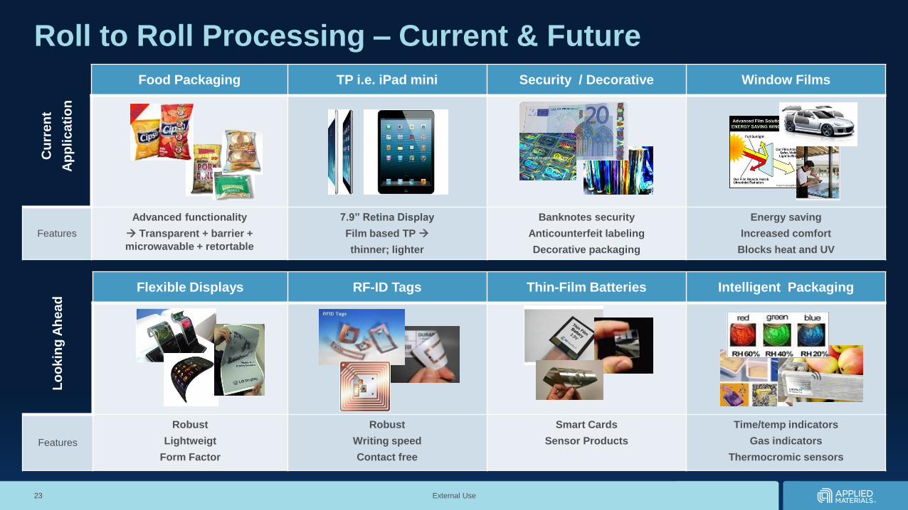
Roll to Roll Processing – Current & Future
23
Cu
rre
nt
Ap
pli
ca
tio
nFood Packaging TP i.e. iPad mini Security / Decorative Window Films
Features
Advanced functionality
Transparent + barrier +
microwavable + retortable
7.9” Retina Display
Film based TP
thinner; lighter
Banknotes security
Anticounterfeit labeling
Decorative packaging
Energy saving
Increased comfort
Blocks heat and UV
Lo
ok
ing
Ah
ea
d
Flexible Displays RF-ID Tags Thin-Film Batteries Intelligent Packaging
Features
Robust
Lightweigt
Form Factor
Robust
Writing speed
Contact free
Smart Cards
Sensor Products
Time/temp indicators
Gas indicators
Thermocromic sensors
External Use
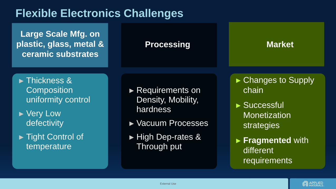
Flexible Electronics Challenges
Large Scale Mfg. on
plastic, glass, metal &
ceramic substrates
► Changes to Supply
chain
► Successful
Monetization
strategies
► Fragmented with
different
requirements
► Requirements on Density, Mobility, hardness
► Vacuum Processes
► High Dep-rates & Through put
Processing
► Thickness & Composition uniformity control
► Very Low defectivity
► Tight Control of temperature
Market
External Use25
Company Profile
Electronics & Display Industries – Flexible Technologies
Global Inflections
Ou
tlin
e
External Use
Summary
External Use
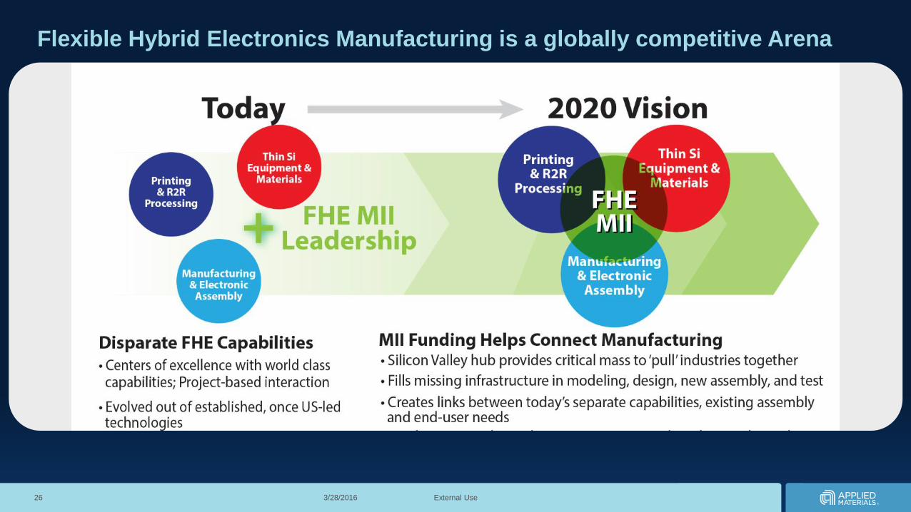
Flexible Hybrid Electronics Manufacturing is a globally competitive Arena
3/28/201626
External Use
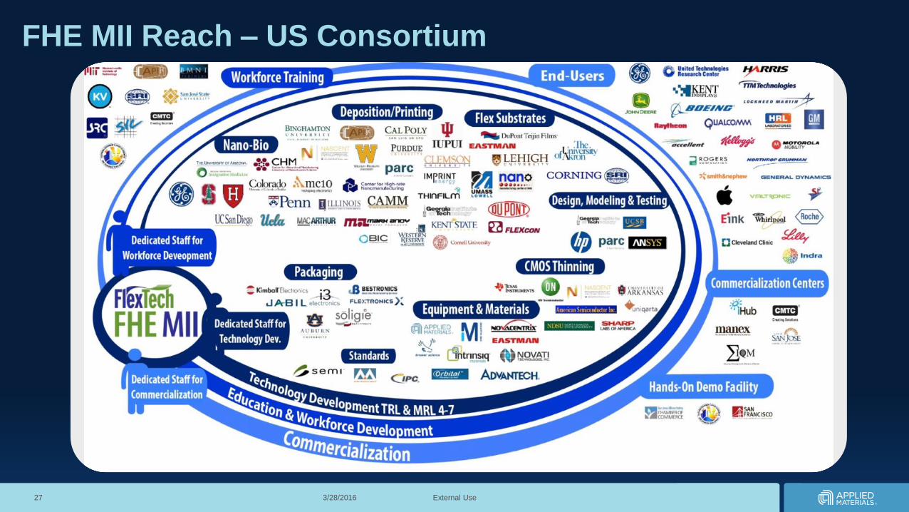
FHE MII Reach – US Consortium
3/28/201627
External Use
Summary
Applied Materials is the global leader in semiconductor & display industries with highly differentiated roll to roll processing equipment
There are many global technology inflections enabled by flexible electronics and display - Materials Engineering at the heart of all these new developments
Technology Solutions exist for Large Scale Manufacturing on plastic, glass, metal and ceramic substrates
Localized Applications require close collaboration between Industry, academia and Government
The FlexiCenter @ IIT Kanpur provides a good platform for Application focused Research & Development
28

29