flexiblecacheerrorprotectionusinganeccfifousers.ece.utexas.edu/~merez/sc09_eccfifo.pdf · the...
TRANSCRIPT

Flexible Cache Error Protection using an ECC FIFO
Doe Hyun YoonElectrical and Computer Engineering
DepartmentThe University of Texas at [email protected]
Mattan ErezElectrical and Computer Engineering
DepartmentThe University of Texas at Austin
ABSTRACT
We present ECC FIFO, a mechanism enabling two-tieredlast-level cache error protection using an arbitrarily strongtier-2 code without increasing on-chip storage. Instead ofadding redundant ECC information to each cache line, ourECC FIFO mechanism off-loads the extra information tooff-chip DRAM. We augment each cache line with a tier-1 code, which provides error detection consuming limitedresources. The redundancy required for strong protection isprovided by a tier-2 code placed in off-chip memory. Becauseerrors that require tier-2 correction are rare, the overhead ofaccessing DRAM is unimportant. We show how this methodcan save 15 − 25% and 10 − 17% of on-chip cache area andpower respectively while minimally impacting performance,which decreases by 1% on average across a range of scientificand consumer benchmarks.
Categories and Subject Descriptors
B.3.2 [Memory Structures]: Design Styles—Cache mem-ories; B.3.4 [Memory Structures]: Reliability, Testingand Fault-Tolerance—Error-checking
General Terms
Reliability, Design
Keywords
soft error, error correction, last-level caches, reliability
1 Introduction
In this paper we present ECC FIFO – a strong error pro-tection architecture aimed at large on-chip last-level caches(LLCs) that minimizes hardware energy and area overheadswhile having minimal impact on performance. Our tech-nique is based on a two-tiered ECC scheme and off-loadsall of the storage required for strong error correction to
This work is supported in part by donations from the Intel corpora-tion
(c) ACM, 2009. This is the author’s version of the work. It is postedhere by permission of ACM for your personal use. Not for redistribu-
tion. The definitive version was published in the Proceedings of SC’09
November 11–20, Portland, Oregon, USA.
off-chip DRAM, potentially leaving only low-cost error de-tection on chip. We store error-correction bits in a FIFOstructure in main memory, instead of in a dedicated on-chipSRAM array. The tiered approach also offers a generaliza-tion of energy-reducing non-uniform error correction tech-niques; low-overhead and low-latency first-tier detection orcorrection is performed on every access to the cache, whilestronger and more costly second-tier correction is only en-gaged once an error is detected.
It is important to minimize the impact on area, power, andapplication performance of strong error protection mecha-nisms because of the continuing increase in soft-error propen-sity. The combination of growing LLC capacity, shrinkingSRAM cell dimensions, and increasing fabrication variabilitythat reduces error margins is leading to a higher soft errorrate (SER) [19, 27, 29]. In particular, recent trends showthat multi-bit burst errors in the array are becoming signif-icant, partially because many memory cells can fall underthe footprint of a single energetic particle strike [19, 21, 26].
Because of these trends, the need to account for high LLCSER and also tolerate multi-bit errors in SRAM arrays is be-coming acute [3]. Researchers have already observed up to16-bit errors in SRAM arrays and are predicting potentiallyhigher counts in the future [1, 19, 21]. The more powerful er-ror protection mechanisms required to correct large numbersof bit flips come at a cost of storing more redundant infor-mation or modifying physical designs, as well as increasedenergy requirements [12, 23]. We aim to reduce the over-heads of providing increased protection against soft errorsin large SRAM arrays. We base our efficient error protec-tion architecture on four important observations that havebeen reported in our recent work:
• While SER is increasing and cannot be ignored at anymemory hierarchy level, error events are still expectedto be extremely rare for a given processor. For in-stance, the mean time to failure (MTTF) of a 32MBcache is around 155 days assuming 10−3FIT/bit [27](FIT: failures in time).
• Every write to the LLC is accompanied by computinginformation required for error correction as well as fordetection. The latency of this operation, however, doesnot affect performance as long as write throughput canbe supported.
• Given that SER is low, the latency and the complex-ity of error correction is not important, since it wouldoccur once every several weeks or months on a givenprocessor.
1

• Much of the data stored in the LLC is also stored else-where in the memory hierarchy (clean cache lines).Replicated data is inherently soft-error tolerant, be-cause correct values can be restored from a copy. Thus,it is enough to detect errors in clean lines.
We combine the observations above into an architecturethat decouples error detection from error correction and thatstores all the redundant information required for correctionin a FIFO structure located in low-cost off-chip DRAM. Un-like prior techniques that reduce the cost of on-chip ECC, in-cluding our recently introduced Memory-Mapped ECC [36],ECC FIFO, which we develop in this paper, does not useany on-chip storage for strong error correction and keepsonly detection, and potentially light weight correction, in-formation on chip. Unlike prior techniques for reducing ECCcost, ECC FIFO does not change the caching behavior of ap-plications, and we demonstrate the importance of this traitin a direct comparison to prior work. Another importantfeature of ECC FIFO is the flexibility it enables in choosingtwo-tiered code combinations. We analyze the advantagesof different two-tier schemes over their one-tier counterpartswith respect to protection and cost.
We evaluate our architecture using full-system cycle-basedsimulation of memory-intensive applications from theSPLASH2 [34], PARSEC [2], and SPEC CPU 2006 [28]suites. We show that the proposed FIFO based approachoutperforms prior techniques for reducing error protectionoverheads on nearly every metric. We estimate 15 − 25%and 10− 17% reductions in area and power-consumption ofa last-level cache respectively, while performance is degradedby only 1.2% on average and by no more than 6%.
The rest of the paper is organized as follows: Section 2 de-scribes related work; Section 3 details our architecture anddiscusses its benefits and requirements; Section 4 discussesprotection capabilities and new tradeoffs enabled by thetwo-tiered approach; Section 5 compares our method withprior work and provides evaluation of ECC FIFO on an out-of-order processor and projections to chip multi-processors(CMPs); and Section 6 concludes the paper.
2 Background and Related Work
In this section we briefly provide background on code-basederror detection and correction mechanisms and prior workon reducing the area and power impact of these mechanisms.
2.1 Information Redundancy
A common solution to address soft errors is to apply errordetecting codes (EDC) and error correcting codes (ECC)uniformly across all cache lines. A cache line is extendedwith an EDC and/or an ECC, and every read or write re-quires error detection/correction or EDC/ECC encoding re-spectively. Typically, error detection only codes are simpleparity codes, while the most common ECCs use Hamming [7]or Hsiao [8] codes that provide single bit error correction anddouble bit error detection (SEC-DED).
When greater error detection is necessary, double bit errorcorrecting and triple bit error detecting (DEC-TED) codes [17],single nibble error correcting and double nibble error detect-ing (SNC-DND) codes [4], and Reed Solomon (RS) codes [24]have also been proposed. They are, however, rarely used incache memories because the overheads of ECC grow rapidlyas correction capability is increased [12]. Instead of us-ing these complex codes, multi-bit correction and detection
Table 1: ECC storage array overheads [27].
SEC-DED SNC-DND DEC-TEDData check
overheadcheck
overheadcheck
overheadbits bits bits bits16 6 38% 12 75% 11 69%32 7 22% 12 38% 13 41%64 8 13% 14 22% 15 23%128 9 7% 16 13% 17 13%
is more commonly achieved by interleaving multiple SEC-DED codes. Table 1 compares the overhead of various ECCschemes. Note that the relative ECC overhead decreases asdata size increases.
Examples from Current Processors.
If the first-level cache (L1) is write through and the LLC(e.g., L2) is inclusive, it is sufficient to provide only errordetection on the L1 data array because the data is repli-cated in L2. Then, if an error is detected in L1, error cor-rection is done by invalidating the erroneous L1 cache lineand re-fetching the cache line from L2. Such an approach isused in the SUN UltraSPARC-T2 [30] and IBM Power 4 [31]processors. The L2 cache is protected by ECC, and becauseL1 is write-through, the granularity of updating the ECCin L2 must be as small as a single word. For instance, theUltraSPARC-T2 uses a 7-bit SEC-DED code for every 32bits of data in L2, an ECC overhead of 22%.
If L1 is write-back (WB), then L2 accesses are at the gran-ularity of a full L1 cache line. Hence, the granularity ofECC can be much larger, reducing ECC overhead. The In-tel Itanium processor, for example, uses a 10-bit SEC-DEDcode that protects 256 bits of data [35] with an ECC over-head of only 5%. Other processors, however, use smallerECC granularity even with L1 write-back caches to providehigher error correction capabilities. The AMD Athlon [9]and Opteron [11] processors, as well as the DEC Alpha21264 [5], interleave 8 8-bit SEC-DED codes for every 64-byte cache line to tolerate more errors per line at a cost of13% additional overhead.
2.2 Reducing Error Correction Overheads
Prior work on reducing on-chip ECC overhead generallybreak the assumption of uniform protection of all cache linesand either sacrifice protection capabilities, when comparedto uniform ECC protection, or utilize different mechanismsto protect clean and dirty cache lines. Kim and Somani [14]suggest parity caching, which compromises error protectionto reduce area and energy costs of ECC by only protectingthose cache lines that have been most recently used in everycache set. Another scheme in this first category is In-CacheReplication (ICR) [38]. ICR increases error protection for asubset of all cache lines, which are accessed frequently, bystoring their replicas in place of cache lines that are predictedto be “dead” and no longer required. Not all cache lines arereplicated leading to a potentially higher uncorrectable errorrate than with the baseline uniform ECC.
An approach to save energy and latency rather than areawas proposed in [25]. The idea is to decouple error detectionfrom error correction and utilize a low-latency andlow-cost EDC for reading, while traditional ECC is com-puted and stored on every write. This ECC is used if anerror is detected. A similar idea was taken further in [16],where the SEC-DED ECC portion of clean cache lines ispower-gated to reduce leakage power, leaving only parityEDC active. Lines that are clean can be recovered from a
2

deeper level in the memory hierarchy and only error detec-tion is necessary.
Kim [13] proposes a method to decrease area in addition toenergy by trading-off performance. His area-efficient schemeallows only one dirty cache line per set in a 4-way set as-sociative cache. If a larger number of lines in a set requireECC (more than one dirty line), a write-back is forced tomake space for the new ECC. In our experiments that ac-curately model the DRAM system (Section 5), we foundthat this additional memory write traffic can significantlydegrade performance. The performance impact can be re-duced at an area and energy cost if more ECC-capable linesare provided in each set. We will refer to this generalizationscheme where n lines per set have ECC as MAXn.
Essentially, the area-efficient scheme above implements aset-associative cache for storing ECC bits. Other work pro-posed a fully-associative replication cache (R-Cache) thatutilizes replication to provide error protection [37]. The R-Cache stores replicas of writes to a L1 cache, and the replicasare accessed on reads to provide detection and correction. Ifthe R-Cache is full, the controller forces a line to be cleanedand written back to L2 so that no data is jeopardized. Al-though its performance impact is minimal, the R-Cache in-creases energy consumption and can only be used with smallL1 caches due to its fully associative structure.
To tolerate multi-bit burst errors, physical bit interleav-ing [23] is used in some commercial designs. By interleavingbits from adjacent cache lines in the physical layout, a multi-bit error caused by a single upset appear as single-bit errorsin multiple cache lines rather than a single line with a multi-bit error. While this method can reduce ECC overhead forburst errors, it requires additional power for accessing ofthe other interleaved words, which are not necessary, andadditional area and delay due to the long word lines and col-umn multiplexer. Hence, physical interleaving is suitable forsmall-scale multi-bit errors, with scaling to higher potentialerror counts results in large performance, area, and poweroverheads [12]. 2D error coding [12] can tolerate multi-biterrors in a more scalable way. Interleaving horizontal andvertical parity codes together provides higher error protec-tion with only a modest increase in ECC storage. 2D coding,however, forces every write being read-modify-write.
Recently, we suggested Memory-Mapped ECC (MME) [36]that uses a two-tiered error protection similar to this work,but differs in how off-loading to memory is managed. MMEstores tier-two error codes as cacheable data in the memoryhierarchy, dynamically and transparently partitioning theLLC into data and error codes. MME’s impact on perfor-mance is low in general, but can be significant because itimpacts the caching behavior of the application, as some ofthe LLC is used for redundant information. This effect isparticularly strong when cache blocking is used to closelymatch the working set with the cache size. ECC FIFO doesnot suffer from this behavior and we explore its benefits overMME in Section 5.
Finally, Lee et al. proposed eager write-back as a way toimprove DRAM bandwidth utilization [15]. It eagerly writesdirty cache lines back to DRAM so that dirty evictions donot contend with demand fetches. Many cache reliabilitystudies (e.g., [13, 16, 36]), including ours, use eager write-back as a way to reduce the average number of dirty cachelines in the LLC.
Last Level Cache
T2EC encoder
T2ECFIFO
CoalesceBuffer
DRAM
k
m
Rest of cache hierarchy
.
.
....
.
.
....
.
.
....
.
.
.
Data T1EC
. . .
S sets
W ways
. . .
B T1
Tag/T2EC
Figure 1: ECC FIFO architecture.
3 ECC FIFO
One of the challenges in designing a large LLC is support-ing strong soft and transient error protection while mini-mizing energy, area, and performance overheads. The mostcommon approaches today extend cache lines with redun-dant information in the form of ECC resulting in overheadsthat are proportional to the degree of error protection; alarger number of errors can be tolerated only at the costof increased redundancy, which increases area and energyleading to lower potential performance. Our ECC FIFO ar-chitecture is designed to minimize energy and area costs ofon-chip redundancy information and increase performanceheadroom. Our technique optimizes the common case ofdetecting errors, and potentially correcting a small num-ber of errors, while providing strong error correction using aunique FIFO structure that off-loads redundant informationto main memory. In the rest of this section, we explain ourtwo-tiered protection scheme in detail and evaluate its im-plementation cost (Section 3.1), followed by a discussion ofa potential limitation to protection due to the finite-natureof the FIFO in DRAM and a solution that allows tradingoff the likelihood of an uncorrectable errors with off-chipstorage requirements (Section 3.2).
3.1 High Level Design and Implementation
We use a two-tiered error protection mechanism, in whichthe mechanisms for detecting errors and correcting errorsare essentially split. The Tier-1 error code (T1EC) is alow-cost code that is accessed on every read and is designedto be decoded with low latency and energy. We providededicated on-chip storage for the T1EC in every cache lineand use it exclusively for error detection or for light-weighterror correction. The Tier-2 error code (T2EC) is morecostly and provides the required redundancy for strong errorcorrection. The T2EC, however, is only computed on a dirtywrite-back into the LLC because clean LLC lines can berecovered from a different level of the memory hierarchy.Just as importantly, the T2EC is only read and decodedon the rare event that the T1EC detects an error that itcannot correct (recall that it is possible to architect T1EC
3

Table 2: Definitions and nominal parameters used for evalu-ation.
LLC parametersnumber of sets S 2048 setsassociativity W 8 wayline size B 64BLLC size S × W × B 1MB
ECC FIFO parameterstag size log
2(S × W ) 14 bits
the coalesce buffer size m 6T1EC size per cache line T1 see Section 4T2EC size per cache line T2 see Section 4T2EC FIFO size k see Section 3.2
OthersDRAM bandwidth BW 5.336GB/seager write-back period Tewb 106 cyclesprocessor clock clock 3GHz
with light-weight correction). Therefore, we do not providededicated on-chip storage for the T2EC and instead writethis redundant information into a FIFO structure allocatedin DRAM (Figure 1). Every time a T2EC is generated, theredundant information is pushed onto the T2EC FIFO alongwith a tag that indicates the corresponding dirty physicalLLC line. Thus, when an error is detected by the T1EC, theT2EC FIFO can be searched starting from the newest entryuntil a matching tag is found and the redundant informationcan be retrieved. The FIFO is simple to implement andallows us to easily identify the T2EC corresponding to anerror with very low management overhead and with efficienttransfer of T2EC data to DRAM.
We now discuss the on-chip area overhead, how to write aline into the LLC and generate the redundant information,how to write T2EC data out to DRAM through a coalescebuffer, how to manage the T2EC FIFO, and how to accessthe LLC and potentially correct any errors.
On-chip Area Overhead
As shown in Figure 1, the on-chip ECC storage overhead isfor T1EC only and is equal to S ×W ×T1 bytes, where S isthe number of LLC sets, W is the LLC associativity, and T1
is the number of bytes required for the T1EC correspondingto single LLC line of B bytes (see Table 2). For example,an 8-way interleaved parity T1EC that detects up to a 15-bit burst error requires just 1 byte of storage for a 64-bytecache line. This is a much smaller overhead than in the con-ventional approach of uniformly providing an 8-way inter-leaved SEC-DED code requiring 8 bytes for each cache line.Both the 8-way interleaved parity T1EC and the conven-tional 8-way interleaved SEC-DED have similar burst-errordetection capability (up to 16-bit bursts for SEC-DED and15-bit bursts for the T1EC), although the SEC-DED codecan detect a larger number of non-burst bit errors. To pro-vide a matching correction capability the T2EC is an 8-wayinterleaved SEC-DED that is stored in the off-chip DRAM.We discuss the off-chip storage overhead in Section 3.2.
LLC Write
We assume the cache level preceding the LLC (e.g., L1 if theLLC is L2) is a write-back cache, hence, the LLC is alwaysaccessed at a coarse granularity of a cache line. When acache line is evicted into the LLC, as well as when a line iswritten into the LLC from DRAM, a T1EC is encoded andwritten along with the data into the LLC. Because a cleanline can be corrected by re-fetching the line from DRAM,a T2EC is encoded only for a dirty line written back into
the LLC from the level above. The encoded T2EC is packedwith a tag , which is a pointer to the corresponding physicaldata line in the LLC. A tag is composed of the set numberand the way number of the cache line so that the T2EC canlater be associated with a detected error. The tag requireslog2(S × W ) bits, e.g., 18 bits for a 16MB LLC with 64Bcache lines. The packed tag/T2EC pair is pushed into acoalesce buffer and then written into the FIFO with DRAM-burst granularity. The coalesce buffer is necessary to achievehigh DRAM throughput because a single tag/T2EC is only10.5 bytes in the example above (8 bytes for an interleavedSEC-DED T2EC and 2.5 bytes for the tag), smaller than theminimum burst size of modern DRAM controllers, which arearchitected for LLC-line granularity (e.g., 64 bytes). Usingthe parameters above, we can coalesce up to 6 tag/T2ECpairs into a single DRAM write-back.
LLC Read
When a cache line is read from the LLC (fill into the preced-ing level, or write-back into DRAM), the T1EC is used todetect and potentially correct errors. If the T1EC detectsan error that it can correct, the LLC controller immediatelycorrects the error and re-writes the cache line. If, on theother hand, the error is not correctable by the T1EC, thena copy of the line within the memory hierarchy is re-fetchedinto the LLC if the line is clean and the T2EC FIFO is usedif the line is dirty.
The first step required to correct an error using T2EC isto identify the FIFO entry that contains the T2EC data.The FIFO is searched sequentially to find the tag, whichcorresponds to the LLC physical line in which the error wasfound. The search starts from the newest FIFO entry, whichcan still be in the on-chip coalesce buffer, and proceeds fromthe current DRAM tail towards the head. Once the mostrecent matching pair is found, the T2EC (and the T1EC,if needed) attempts to correct the errors. Thus, the worstcase penalty of T2EC error correction is the required time toread and compare all tag/T2EC pairs from the FIFO. Thistakes roughly k × (B/m)/BW seconds, where k is the sizeof the FIFO in number of pairs, m is the number of pairsin a cache line and BW is the expected throughput of theDRAM channel in bytes/sec (see Table 2). For instance, theworst case correction latency is around 1.66 ms when k is onemillion entries, m is 6, B is 64 bytes, and BW is 6.4GB/s.This overhead, however, is entirely negligible given the rareoccurrence of an error that requires T2EC for correction,which we estimate at one error every 155 days for a 32MBcache in today’s technology [27, 29].
T2EC FIFO
We propose to use a large circular FIFO buffer in the mainmemory space to store the T2EC information. The FIFOhas two significant advantages over other T2EC storage op-tions: (i) a FIFO allows for arbitrary coalescing with a triv-ial and small on-chip buffer that can still maximize DRAMthroughput; and (ii) a FIFO is easy to manage in softwareand provides a clear way to identify the most recent up-date to a LLC physical line’s T2EC data. Information onthe FIFO size and base address is stored within the LLCcontroller and can be set by privileged hypervisor or O/Sinstructions, or through the BIOS.
One caveat to using a circular buffer is that a T2EC pushinto the FIFO overwrites the oldest entry. If the physicalcache line that corresponds to the overwritten T2EC FIFO
4

0
0.1
0.2
0.3
0.4
0.5
0.6
0 20 40 60 80 100
FIFO size [thousand entries]
Probability of T2EC unprotected
Fevict
Freuse
Figure 2: Punprot, Freuse, and Fevict in the lbm application
entry has not been modified or evicted from the LLC thenits T2EC information is overwritten and lost. At that point,the line becomes T2EC unprotected and the system will notbe able to recover from an error within it.
3.2 T2EC Overwrite and Unprotected Lines
In this section, we analyze the effects of the T2EC FIFOsize on T2EC protection capability, which we define as theprobability that a T2EC cannot correct the LLC line dueto a T2EC overwrite in the circular buffer (Punprot). Eventhough the buffer is finite, the probability of unprotectedlines is small for two main reasons: (i) inherent memory ac-cess patterns in applications that limit the lifetime of dirtylines in the LLC through reuse and capacity/conflict evic-tions; and (ii) limiting dirty line lifetime by programmingthe LLC controller to periodically clean dirty lines.
3.2.1 Reused and Evicted Dirty Lines
In many applications the natural access pattern leads torelative short lifetime of dirty lines in the LLC. Cache linesare often re-written by the application as new results aregenerated, rendering earlier computed T2EC data stale andunnecessary. In other cases, LLC lines are evicted to makeroom for new lines being fetched, and again any existingcorresponding T2EC data in the FIFO becomes obsolete.We denote the fraction of T2EC entries that correspond toreused lines in the LLC as Freuse and the fraction of entriescorresponding to evicted lines as Fevict.
For example, lbm from the SPEC CPU 2006 suite [28]has streaming memory access patterns, and hence, the vastmajority of dirty lines are written-back into DRAM beforea T2EC overwrite occurs. Simulation results (parameters asdescribed in Section 5) show that Fevict goes up rapidly asthe FIFO size is increased from 15K to 30K entries so thatthe probability of T2EC unprotected reaches 0 when theFIFO is larger than 30K entries, which is 313KB of DRAMspace (Figure 2).
3.2.2 Periodically Cleaning Dirty Lines
Although some applications (such as lbm) do not suffer fromT2EC unprotected with a reasonable FIFO size, other ap-plications may cause overwrites leading to unprotected linesregardless of the FIFO depth. We utilize the previously pro-posed eager write-back technique [15] to bound the lifetimeof a dirty line in the LLC. We explain this in detail and de-rive a model to analyze the T2EC unprotected probabilitywith eager write-back.
The original eager write-back technique, proposed in [15],opportunistically writes dirty lines into DRAM when a dirtyline is in the least-recently used position and a DRAM issueslot is available. This reduces pressure on DRAM when de-mand fetches are necessary and increases performance. Weutilize a more predictable approach, which retains the per-formance advantages, in which lines are periodically probed
dirty line
eviction to LLC
eager write-back scan
time
Tewb cycles Tewb cycles
Tewb cycles Tewb cycles
eager write-back scan
-- not old to be cleaned
eager write-back scan
-- old enough -- clean
Figure 3: An example time-line of dirty line eviction to theLLC and eager write-back.
Tewb 2Tewb
PD(t)1
0 t
Figure 4: Probability that a dirty cache line remains dirty intime.
and written back if dirty. This is similar to the policy used incache error protection studies [13, 16] and decay caches [10].Our eager write-back implementation scans each cache linewith a predetermined period, Tewb cycles, and eagerly writesa dirty line older than the period.
Figure 3 shows an example time-line of a dirty line inthe LLC, from the time it is evicted into the LLC until thetime it is cleaned by an eager write-back. Each cache line isscanned once per Tewb cycles so that a dirty line is eagerlywritten back to DRAM within a maximum of 2×Tewb cyclesafter the line is evicted into the LLC. Based on this observa-tion and the fact that the periodic scanning is independentof the eviction times, we can define PD(t) as the expectedprobability that a dirty cache line that was written into theLLC at time t = 0 remains dirty at time t, as shown inFigure 4. Since eager write-back does not clean dirty linesyounger than Tewb cycles, PD(t) = 1 for the first Tewb cy-cles, after which PD(t) decreases linearly until it reaches 0at time t = 2× Tewb cycles. Figure 5 illustrates the two po-tential time-lines of a dirty LLC line that is neither evictednor reused with respect to being cleaned by an eager write-back or overwritten in the T2EC FIFO. Figure 5(a) depictsthe case that a line is cleaned by an eager write-back beforeits T2EC data is overwritten and is thus fully protected,whereas Figure 5(b) shows a window of vulnerability open-ing if the T2EC is overwritten before the line is written back.
To summarize the discussion above, the factors determin-ing whether a line becomes T2EC unprotected are the pe-riod of time in which a T2EC entry is required to protectthe cache line (the T2EC entry’s valid-time) and the timefor the T2EC to be overwritten in the FIFO (its overwrite-time); when a T2EC entry’s valid-time is longer than itsoverwrite-time, the cache line becomes T2EC unprotected.The valid-time is the property of the LLC and memory ac-cess pattern; the time it takes for the line to be cleaned byan eager write-back determines the valid-time unless the lineis reused or evicted before it is cleaned. The overwrite-timeis a function of the FIFO depth and the rate at which dirtylines are written into the LLC (property of memory accesspattern and parameters of the caches closer to the core). Be-cause the valid- and overwrite-times are application-specificand dynamic, we model their impact on unprotected lines
5

dirty line
eviction to LLC
T2EC push to
the FIFO … (k-1) additional pushes …k-th T2EC push
now, the first ECC is overwritten
…time
clean
the T2EC is no longer needed
(a) a protected case
…time
cleanWindow of
vulnerability
dirty line
eviction to LLC
T2EC push to
the FIFO … (k-1) additional pushes …k-th T2EC push
now, the first ECC is overwritten
(b) an unprotected case
Figure 5: Time-lines of dirty lines with T2EC pushes to the FIFO.
00.020.040.060.080.10.120.14
0
0.2
0.4
0.6
0.8
1
1.2
0 1 2 3 4
DT2E
C(t)
P D(t)
time [M cycles]
PD(t)
DT2EC(t)5K FIFO DT2EC(t)
10K FIFO
Figure 6: Examples of DT2EC(t) for 5k and 10k entry FIFOsfrom omnetpp application overlaid on PD(t) when Tewb is 1Mcycles.
1.00E-10
1.00E-09
1.00E-08
1.00E-07
1.00E-06
1.00E-05
1.00E-04
1.00E-03
1.00E-02
1.00E-01
1.00E+00
0 10 20 30 40 50 60 70 80 90 100
Pro
babili
ty o
f T2E
C u
np
rote
cte
d
FIFO size [thousand entries]
FFT CHOLESKY OCEAN RADIX
canneal fluidanimate mcf hmmer
libquantum omnetpp lbm milc
sphinx3 dedup freqmine bzip2
00
Figure 7: Probability of T2EC unprotected when Tewb is 1Mcycles. A FIFO larger than 40k entries is required only inthree applications: dedup, freqmine, and bzip2.
using a probability density function of the overwrite-time,DT2EC(t). DT2EC(t) is the distribution of T2EC overwrite-time that a T2EC entry that was computed at time t = 0is overwritten at time t > 0. Figure 6 shows examples ofDT2EC(t) from omnetpp with different FIFO sizes. A largerFIFO shifts DT2EC(t) towards longer overwrite times so thateager write-back cleans nearly all the dirty lines before theT2EC is overwritten. We can now write the probability ofan unprotected line as in Equation 1.
Punprot = (1−Freuse−Fevict)×
Z
∞
0
PD(t)×DT2EC(t) dt (1)
We used a detailed simulator, described in Section 5, tocollect T2EC overwrite-time information for a variety ofbenchmark applications and a range of FIFO sizes. We thenapplied the model of Equation 1 and compared the resultingexpected fraction of unprotected LLC lines to that from thecycle-accurate simulation. Although we do not present thedetailed comparison results in this paper, the model and thesimulation agreed to within 1%.
Impact of FIFO Size and Eager Write-Back Period
Figure 7 shows the decrease in probability of T2EC unpro-tected as the size of the FIFO increases for a range of appli-cations when the eager write-back period is 1M cycles. Allbut 3 of the applications (dedup, freqmine, and bzip2) arefully protected with a FIFO of 40K entries requiring only417KB of DRAM storage. The deepest FIFO required toavoid overwrites with Tewb = 1M cycles is 100K-entries forbzip2, requiring about 1MB of DRAM storage. Figure 8shows the effects of varying Tewb on a few representativeapplications. All but 4 of the applications evaluated be-haved similarly to OCEAN of the SPLASH2 suite, requiringa FIFO smaller than 100K entries even with Tewb = 5Mcycles. RADIX, bzip2, freqmine, and dedup required deeperbuffers, with dedup requiring a 220K-entry (2.5MB) bufferwith Tewb = 5M cycles.
Guaranteeing No T2EC Unprotected Lines.
If the T2EC FIFO is sufficiently large, then eager write-backwill always clean a dirty line before the corresponding T2ECis overwritten. With eager write-back, the maximum T2ECvalid-time is 2 × Tewb cycles so we need to choose a FIFOdeep enough to make the minimum T2EC overwrite-timelonger than the maximum valid-time. The minimum T2ECoverwrite-time is k/R, where R is the maximum FIFO fillrate, and a FIFO greater than 2× Tewb ×R prevents T2ECunprotected.
The maximum FIFO fill rate is essentially the maximumpossible rate of dirty line writes into the LLC. At worse, ev-ery store instruction can cause a dirty line eviction into theLLC. Alternatively, the fill rate may be limited by the totalDRAM write bandwidth (to fill the FIFO) or the bandwidthof the LLC controller. In our simulated system (see Ta-ble 5), the DRAM write bandwidth sets the tightest bound.The FIFO size required is 2 × Tewb × m/B × BW/clock,where clock is the clock frequency of eager write-back op-erations. This corresponds to a FIFO of 346, 070 entriesrequiring 3.6MB. While this is a fairly large buffer, its sizeis very small compared to today’s main-memory capacitiesand replaces valuable on-chip area.
Sensitivity to Cache Size
Intuitively, a larger L1 or a smaller L2 will reduce the num-ber of T2EC unprotected lines; a larger L1 reduces therate of dirty evictions into the LLC, and as a result, T2ECoverwrite-time increases. Similarly, a smaller L2 will causecache lines to be replaced more often, due to capacity con-straints, which then decreases T2EC valid-time. We ransimulations varying the L1 size between 32−128KB and theL2 size between 512 − 2048 KB. The behavior of T2EC un-protected is as expected and described above. The overallimpact of cache sizes is relatively small and we omit the fullresults for brevity. The conclusion is that the FIFO depth
6

1.00E-10
1.00E-09
1.00E-08
1.00E-07
1.00E-06
1.00E-05
1.00E-04
1.00E-03
1.00E-02
1.00E-01
1.00E+00
0 20 40 60 80 100
Pro
bab
ility
of T
2E
C u
np
rote
cte
d
FIFO size [thousand entries]
0.1M0.3M0.5M0.75M1M2M3M4M5M
0
(a) OCEAN
1.00E-10
1.00E-09
1.00E-08
1.00E-07
1.00E-06
1.00E-05
1.00E-04
1.00E-03
1.00E-02
1.00E-01
1.00E+00
0 20 40 60 80 100 120 140 160 180 200 220 240
Pro
ba
bili
ty o
f T2E
C u
np
rote
cte
d
FIFO size [thousand entries]
0.1M0.3M0.5M0.75M1M2M3M4M5M
0
(b) dedup
1.00E-10
1.00E-09
1.00E-08
1.00E-07
1.00E-06
1.00E-05
1.00E-04
1.00E-03
1.00E-02
1.00E-01
1.00E+00
0 20 40 60 80 100 120 140 160 180 200
Pro
ba
bili
ty o
f T2E
C u
npro
tecte
d
FIFO size [thousand entries]
0.1M0.3M0.5M0.75M1M2M3M4M5M
0
(c) RADIX
1.00E-10
1.00E-09
1.00E-08
1.00E-07
1.00E-06
1.00E-05
1.00E-04
1.00E-03
1.00E-02
1.00E-01
1.00E+00
0 20 40 60 80 100 120 140 160 180 200
Pro
ba
bili
ty o
f T2E
C u
np
rote
cte
d
FIFO size [thousand entries]
0.1M0.3M0.5M0.75M1M2M3M4M5M
0
(d) bzip2
Figure 8: Probability of T2EC unprotected varying Tewb.
required to eliminate the possibility of T2EC unprotectedlines is unchanged in most applications and only changes by5 − 10K in four of the 8 applications we tested.
4 Error Protection Tradeoffs
In this section, we evaluate improvements in protection ca-pabilities and discuss new tradeoffs enabled by the two-tiered approach. One of the main advantages of our two-tiered error protection is the flexibility it provides in choos-ing the T1EC and T2EC. The most important design con-siderations of applying ECC FIFO are as follows:
• The T1EC should be chosen to minimize on-chip over-head as it is stored along with every cache line.
• T1EC should be computed with low latency and max-imize error detection; correction can be left to T2EC.
• The T2EC size determines overall protection capabil-ities, but large T2ECs increase DRAM traffic, whichdegrades the performance of some applications.
• The T2EC FIFO depth and eager write-back periodmust be selected to limit the number of unprotectedlines.
With these considerations, Table 3 describes the configu-rations and burst error protection capabilities of a numberof one-tiered baseline error codes as well as two-tiered errorcodes. All of the two-tiered codes have identical T2EC size(8B) per 64B cache line, hence the impact on performancewill be roughly the same. This leaves the tradeoff to be be-tween the error protection capability (T1EC detection andT2EC correction) and on-chip area (T1EC size).
The PS configuration (parity T1EC and SEC-DED T2EC)allows us to directly compare our architecture to the base-line one-tier 8-way interleaved Hamming SEC-DED codes(S), which are commonly used in related and prior work.The two-tiered PS provides the same bursty error correctioncapability (up to 8-bit bursts) as the one-tier SEC-DED (S)with reduced on-chip area. The number of detectable er-rors is different, however. The interleaved parity can detect
bursts up to 15 bits long, whereas the conventional inter-leaved SEC-DED Hamming codes can detect up to 16-bitbursts (8 interleaved double bit errors). The codes also differin their detection capability for non-burst multi-bit errors,which we evaluate later in this section using error injection.
The PN (parity T1EC and nibble-based SNC-DND T2EC)and PB (parity T1EC and byte-based RS T2EC) configura-tions can correct even longer bursts. Correction capabilityis up to 4 nibbles (13–16 bits) and 4 bytes (25–32 bits) re-spectively, while the on-chip overhead is still very low; eventhe 32-way parity T1EC of PB requires only 4 bytes, halfthe space of the baseline (S).
The SD configuration uses a DEC-TED code, which is sep-arable into an 8-bit SEC-DED, with an additional 8 bits pro-viding detection and correction for one more bit error [22].In our two-tier SD, the 8-bit SEC-DED portion is the T1ECthat correct nearly all errors, those that have up to 8-bitbursts, with very low latency. The T2EC DEC-TED, whichis constructed from the 8 bits stored on chip in the T1ECand the 8 bits that are retrieved from the T2EC FIFO, isused only in the very rare case of an error that was detectedby the T1EC but cannot be corrected by it. Note that theT1EC has only half the on-chip storage overhead of the one-tier DEC-TED configuration (D).
Storage, Energy, and Latency Overheads
The T2EC encoding complexity plays an important role, af-fecting both energy requirements and latency. The latencyof computing T2EC, however, can be hidden, because thereare no dependencies on T2EC data. Thus, choosing differ-ent T2ECs with regards to the encoding complexity onlyimpacts energy consumption, which is relatively low.
Table 4 compares area overheads, leakage power, and ar-ray energy per access of the two-tiered error protection,MAXn, and baseline schemes. We use CACTI 5 [32] toreport the properties of a 1MB LLC and related ECC in a45nm process. Our architecture only dedicates on-chip stor-age to the T1EC and significantly reduces the area and leak-
7
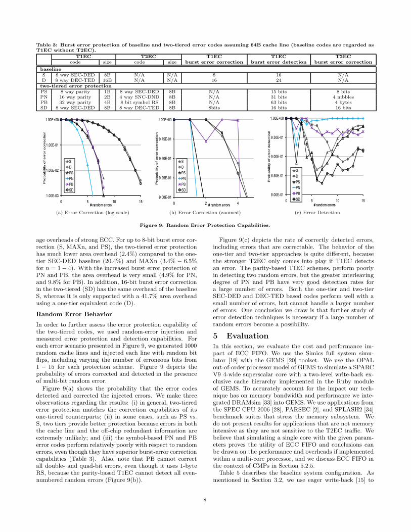
Table 3: Burst error protection of baseline and two-tiered error codes assuming 64B cache line (baseline codes are regarded asT1EC without T2EC).
T1EC T2EC T1EC T1EC T2ECcode size code size burst error correction burst error detection burst error correction
baselineS 8 way SEC-DED 8B N/A N/A 8 16 N/AD 8 way DEC-TED 16B N/A N/A 16 24 N/Atwo-tiered error protectionPS 8 way parity 1B 8 way SEC-DED 8B N/A 15 bits 8 bitsPN 16 way parity 2B 4 way SNC-DND 8B N/A 31 bits 4 nibblesPB 32 way parity 4B 8 bit symbol RS 8B N/A 63 bits 4 bytesSD 8 way SEC-DED 8B 8 way DEC-TED 8B 8bits 16 bits 16 bits
1.00E-03
1.00E-02
1.00E-01
1.00E+00
0 5 10 15
Prob
abilit
y of e
rror c
orre
ctio
n
# random errors
SDPSPNPBSD
(a) Error Correction (log scale)
9.00E-01
9.25E-01
9.50E-01
9.75E-01
1.00E+00
0 2 4
Prob
abilit
y of e
rror c
orre
ctio
n
# random errors
SDPSPNPBSD
(b) Error Correction (zoomed)
8.00E-01
8.50E-01
9.00E-01
9.50E-01
1.00E+00
0 5 10 15
Prob
abilit
y of e
rror d
etec
tion
# random errors
SDPSPNPBSD
(c) Error Detection
Figure 9: Random Error Protection Capabilities.
age overheads of strong ECC. For up to 8-bit burst error cor-rection (S, MAXn, and PS), the two-tiered error protectionhas much lower area overhead (2.4%) compared to the one-tier SEC-DED baseline (20.4%) and MAXn (3.4% − 6.5%for n = 1− 4). With the increased burst error protection ofPN and PB, the area overhead is very small (4.9% for PN,and 9.8% for PB). In addition, 16-bit burst error correctionin the two-tiered (SD) has the same overhead of the baselineS, whereas it is only supported with a 41.7% area overheadusing a one-tier equivalent code (D).
Random Error Behavior
In order to further assess the error protection capability ofthe two-tiered codes, we used random-error injection andmeasured error protection and detection capabilities. Foreach error scenario presented in Figure 9, we generated 1000random cache lines and injected each line with random bitflips, including varying the number of erroneous bits from1 − 15 for each protection scheme. Figure 9 depicts theprobability of errors corrected and detected in the presenceof multi-bit random error.
Figure 9(a) shows the probability that the error codesdetected and corrected the injected errors. We make threeobservations regarding the results: (i) in general, two-tierederror protection matches the correction capabilities of itsone-tiered counterparts; (ii) in some cases, such as PS vs.S, two tiers provide better protection because errors in boththe cache line and the off-chip redundant information areextremely unlikely; and (iii) the symbol-based PN and PBerror codes perform relatively poorly with respect to randomerrors, even though they have superior burst-error correctioncapabilities (Table 3). Also, note that PB cannot correctall double- and quad-bit errors, even though it uses 1-byteRS, because the parity-based T1EC cannot detect all even-numbered random errors (Figure 9(b)).
Figure 9(c) depicts the rate of correctly detected errors,including errors that are correctable. The behavior of theone-tier and two-tier approaches is quite different, becausethe stronger T2EC only comes into play if T1EC detectsan error. The parity-based T1EC schemes, perform poorlyin detecting two random errors, but the greater interleavingdegree of PN and PB have very good detection rates fora large number of errors. Both the one-tier and two-tierSEC-DED and DEC-TED based codes perform well with asmall number of errors, but cannot handle a larger numberof errors. One conclusion we draw is that further study oferror detection techniques is necessary if a large number ofrandom errors become a possibility.
5 Evaluation
In this section, we evaluate the cost and performance im-pact of ECC FIFO. We use the Simics full system simu-lator [18] with the GEMS [20] toolset. We use the OPALout-of-order processor model of GEMS to simulate a SPARCV9 4-wide superscalar core with a two-level write-back ex-clusive cache hierarchy implemented in the Ruby moduleof GEMS. To accurately account for the impact our tech-nique has on memory bandwidth and performance we inte-grated DRAMsim [33] into GEMS. We use applications fromthe SPEC CPU 2006 [28], PARSEC [2], and SPLASH2 [34]benchmark suites that stress the memory subsystem. Wedo not present results for applications that are not memoryintensive as they are not sensitive to the T2EC traffic. Webelieve that simulating a single core with the given param-eters proves the utility of ECC FIFO and conclusions canbe drawn on the performance and overheads if implementedwithin a multi-core processor, and we discuss ECC FIFO inthe context of CMPs in Section 5.2.5.
Table 5 describes the baseline system configuration. Asmentioned in Section 3.2, we use eager write-back [15] to
8

Table 4: Area, leakage power, and array energy per read access.
baseline MAXn two-tiered error protectionno ECC S D MAX1 MAX2 MAX4 PS PN PB SD
Leakage Power (W) 1.4 1.6 1.8 1.5 1.5 1.6 1.4 1.5 1.5 1.6Array Energy per Read (nJ) 2.0 2.4 2.9 2.1 2.1 2.7 2.1 2.1 2.2 2.4Area (mm2) 10.0 12.0 14.1 10.3 10.4 10.6 10.2 10.5 10.9 12.0ECC area overhead (%) - 20.7 41.7 3.4 4.2 6.5 2.4 4.9 9.8 20.7
Table 5: Simulated system parameters.
Processor SPARC V9 ISACore 4-wide superscalar (3GHz)L1 Cache split I/D cache
each 64KB2-way set associative64B cache lineswrite-back1 cycle latency
L2 Cache unified 1MB cache8-way set associativeL1 exclusive64B cache lineseager write-back (Tewb = 106 cycle)L2 latency is 12 cycles,including ECC encoding/decoding
DRAM single channel DDR2 DRAM (5.336GB/s)667MHz 64-bit data busopen pageRead and Instruction Fetch First
0.9
1
1.1
1.2
1.3
1.4
CHOLE
SKY
FFT
OCEA
N
RAD
IX
cann
eal
dedu
p
fluidan
imate
freqm
ine
bzip2
mcf
hmmer
libqu
antum
omne
tpp
milc lbm
sphinx
3
Avg.
SPLASH2 PARSEC SPEC2006
Normalized
Exe
cutio
n Tim
e
Max1Max2Max4MMEECC FIFO
Figure 10: Normalized execution time.
limit the lifetime of dirty lines in the LLC and to improve thebaseline performance; eager write-back improves the base-line performance by 6–10% in most applications and 26% inlibquantum. In lbm and bzip2, however, eager write-backdegrades performance significantly and we disable it for theprior-work techniques, as it is not needed for correctness orprotection. We also disable eager write-back for ECC FIFOin lbm, because the probability of T2EC unprotected is neg-ligible, even without eager write-back. We keep eager write-back at 1M cycles for bzip2 with ECC FIFO to maintaina low T2EC unprotected rate. Note that we applied dif-ferent eager write-back periods for fluidanimate (0.25M)and libquantum (1.2M) to optimize the performance of thebaseline scheme.
5.1 Workloads
We use a mix of the SPLASH2 [34], PARSEC [2], and SPECCPU 2006 [28] workloads. We concentrated on applicationswith large working sets that stress the memory hierarchyand highlight the differences between our architecture andprior work. For the detailed cycle-based simulations, weran the applications from SPLASH2 and PARSEC to com-
1.40E+09
1.60E+09
1.80E+09
2.00E+09
2.20E+09
2.40E+09
2.60E+09
256KB 512KB 1MB 2MB
Exec
utio
n Ti
me
[cyc
le]
LLC size
BaselineMMEECC FIFO
Figure 11: OCEAN 258× 258 performance of the baseline, MME,and ECC FIFO varying LLC size.
pletion using a single thread and small to medium problemsizes: tk15.O for CHOLESKY; 64K samples for FFT; a 514×514grid for OCEAN; 1M samples for RADIX, and the simsmall in-puts for all PARSEC applications. For the SPEC CPU 2006workloads, we used SimPoint [6] to extract five representa-tive regions of 200M instructions and report their weightedsums.
5.2 Performance Results and Analysis
This section contains multiple subsections in which we eval-uate overall performance results and compare the impactof ECC FIFO to that of MAXn schemes [13] and Memory-Mapped ECC [36]; analyze LLC power consumption in vari-ous error coding schemes discussed in Section 4 and show thepotential of saving LLC power consumption by off-loadingthe T2EC to DRAM; evaluate the impact of additional DRAMtraffic needed for off-loading the T2EC to DRAM, whichonly degrades performance if it competes with demand fetches;and analyze sensitivity to DRAM bandwidth to assess theperformance impact of ECC FIFO on CMPs, where DRAMbandwidth is more scarce.
5.2.1 Impact on Performance
Figure 10 compares the execution times of MAXn, MME,and ECC FIFO normalized to the execution time of thebaseline configuration. As shown, the impact on applica-tion performance of ECC FIFO is minimal, with an aver-age performance penalty of less than 1.2% and a maximumdegradation of just under 6% in bzip2 and 4% in lbm. Thedegradation in bzip2 is not from ECC traffic, but ratherbecause of the use of eager write-back to bound the life-time of dirty lines (recall that eager write-back is enabledonly with ECC FIFO for bzip2). ECC FIFO without eagerwrite-back degrades the performance of bzip2 by only 1.3%,but requires a larger FIFO of 2MB in DRAM. These resultsare encouraging because of the benefits our scheme provides
9

1
1.2
1.4
1.6
1.8
2
2.2
S PS PN PB D SD S PS PN PB D SD S PS PN PB D SD S PS PN PB D SD S PS PN PB D SD S PS PN PB D SD S PS PN PB D SD S PS PN PB D SDCHOL FFT OCEAN RADIX canneal ddedup fluidanimate freqmine
SPLASH2 PARSEC
LLC
Pow
er [W
]
LLC WrLLC RdLeakage
(a) SPLASH2 and PARSEC
1
1.2
1.4
1.6
1.8
2
2.2
S PS PN PB D SD S PS PN PB D SD S PS PN PB D SD S PS PN PB D SD S PS PN PB D SD S PS PN PB D SD S PS PN PB D SD S PS PN PB D SD S PS PN PB D SDbzip2 mcf hmmer libquantum omnetpp milc lbm sphinx3
SPEC Avg.
LLC
Pow
er [W
]
(b) SPEC CPU 2006
Figure 12: LLC power consumption estimated with CACTI 5 for a 1MB, 8-way, 64B cache line LLC in 45nm technology.
0
5
10
15
20
25
30
35
40
45
50
Ba
se
MA
X1
MA
X2
MA
X4
MM
E
FIF
O
Ba
se
MA
X1
MA
X2
MA
X4
MM
E
FIF
O
Ba
se
MA
X1
MA
X2
MA
X4
MM
E
FIF
O
Ba
se
MA
X1
MA
X2
MA
X4
MM
E
FIF
O
Ba
se
MA
X1
MA
X2
MA
X4
MM
E
FIF
O
Ba
se
MA
X1
MA
X2
MA
X4
MM
E
FIF
O
Ba
se
MA
X1
MA
X2
MA
X4
MM
E
FIF
O
Ba
se
MA
X1
MA
X2
MA
X4
MM
E
FIF
O
CHOLESKY FFT OCEAN RADIX canneal dedup fluidanimate freqmine
SPLASH2 PARSEC
Requ
est
per
thou
san
d i
nstr
uction
s
T2EC Rd/Wr
Cleaning
eager write-back
DRAM Wr
DRAM Rd
(a) SPLASH2 and PARSEC
0
5
10
15
20
25
30
35
40
45
50
Base
MA
X1
MA
X2
MA
X4
MM
E
FIF
O
Base
MA
X1
MA
X2
MA
X4
MM
E
FIF
O
Base
MA
X1
MA
X2
MA
X4
MM
E
FIF
O
Base
MA
X1
MA
X2
MA
X4
MM
E
FIF
O
Base
MA
X1
MA
X2
MA
X4
MM
E
FIF
O
Base
MA
X1
MA
X2
MA
X4
MM
E
FIF
O
Base
MA
X1
MA
X2
MA
X4
MM
E
FIF
O
Base
MA
X1
MA
X2
MA
X4
MM
E
FIF
O
bzip2 mcf hmmer libquantum omnetpp milc lbm sphinx3
SPEC 2006
(b) SPEC CPU 2006
Figure 13: DRAM traffic comparison.
in reducing on-chip area and leakage power by minimizingdedicated on-chip ECC storage. The MAXn technique, onthe other hand, requires significant tradeoff between perfor-mance loss and area gains. MAX1 averages over 8% perfor-mance loss with several applications experiencing 10 - 36%degradation, MAX2 degrades 8% on average while libquan-tum is significantly degraded by 30%, and MAX4 performsonly slightly better than ECC FIFO and MME. MAX4 re-quires, however, much more area than MME and ECC FIFOas shown in Table 4.
The anomalous behavior of OCEAN, fluidanimate, fre-
qmine, bzip2, mcf, libquantum, and sphinx3, where the per-formance of MAX2 and MAX4 is slightly better than base-line, is a result of increased eager write-backs for lines thatare being forced clean in order to guarantee protection. Wealso note that applications with small working sets, such asWATER-NSQUARED (SPLASH2) and blackscholes (PAR-SEC) experience no performance drop with ECC FIFO, aswell as with MAXn and MME, and we do not report theirresults. All other applications from the benchmark suites,which we do not discuss in this paper, are also unaffectedby the two-tiered approach.
5.2.2 Comparison with MME
MME’s performance degradation is 1.3% on average (Fig-ure 10), which is comparable to that of the ECC FIFO
(1.2% on average). Note that the area / error protectiontradeoff in MME is the same as that of ECC FIFO be-cause both schemes use two-tiered error protection and off-loading to DRAM. MME, however, can impact performancesignificantly when the working set of an application closelymatches the LLC size. Figure 11 compares the executiontimes of OCEAN with a 258× 258 grid on the baseline, MME,and ECC FIFO configurations as the LLC size is varied. Asthe LLC size grows from 512KB to 1MB, the baseline per-formance is improved by 26%. ECC FIFO’s performancepenalty is consistently less than 1% across all LLC sizes.MME, however, degrades performance significantly (10%)with a 1MB LLC since the effective LLC size is reduced bysharing the LLC between data and error codes.
5.2.3 Impact on LLC
ECC FIFO bypasses the LLC to accesses T2EC information,and thus does not change the caching behavior and only im-pacts the operation of the DRAM system. ECC FIFO, how-ever, reduces power consumption of the LLC in two ways:decreased energy per access and reduced leakage power.
Figure 12 compares LLC power consumption of the base-line (S and D) and the ECC FIFO (PS, PN, PB, and SD)estimated using CACTI 5 [32] for the cache parameters inTable 5 in a 45nm technology. PS saves 9% of LLC powerconsumption compared to S, while SD, PN, and PB consume
10

0.91
1.11.21.31.41.51.6
CHOLE
SKY
FFT
OCEA
N
RAD
IX
cann
eal
dedu
p
fluidan
imate
freqm
ine
bzip2
mcf
hmmer
libqu
antum
omne
tpp
milc lbm
sphinx
3
Avg.
SPLASH2 PARSEC SPEC2006
Normalized
Exe
cutio
n Tim
eMax1Max2Max4MMEECC FIFO
Figure 14: Normalized execution time (2.667 GB/s DRAMbandwidth).
10%, 17%, and 15% less power than D, respectively. Notethat PS and SD provide similar error protection as S andD, respectively, and PN and PB can protect against evenlonger error bursts, even compared to D.
5.2.4 Impact on DRAM Traffic
Figure 13 shows the total DRAM traffic broken down intocomponents of data reads and writes of LLC lines (DRAMRd and DRAM Wr), eager write-backs of cache lines (eagerwrite-back), MAXn writes for cleaning lines (Cleaning), andT2EC traffic of MME and ECC FIFO (T2EC Rd/Wr). Al-though MAXn does not increase overall memory traffic bymuch in most cases, the type of traffic and its timing dif-fer significantly from the baseline. Unlike eager write-backtraffic, which is scheduled during idle DRAM period [15],MAXn’s cleaning writes compete with demand fetches anddegrade performance as shown in Figure 10. More detailedanalysis on how MAXn’s cleaning traffic degrades perfor-mance can be found in [36]. Compared to the baseline, ECCFIFO increases memory traffic by 9% on average, which ismuch larger than MME’s traffic penalty (2%). It is, how-ever, not critical to performance in that T2EC write-backis one-way traffic and can be scheduled during idle DRAMperiod.
5.2.5 Multi-Core Considerations
We have so far discussed and evaluated ECC FIFO in thecontext of a single core and now briefly discuss multi-coreand multi-processor implications. ECC FIFO is easily in-tegrated with any cache coherence mechanism because theT2EC FIFO in DRAM is inherently private. On the otherhand, the increased traffic of ECC FIFO may hurt the per-formance due to relatively lower DRAM bandwidth per corein CMPs. We evaluated ECC FIFO in a system with lowDRAM bandwidth of only 2.667 GB/s, which is half thebandwidth of the baseline system. As Figure 14 shows, therelative performance of ECC FIFO is not sensitive to mem-ory bandwidth.
6 Conclusions and Future Work
This paper presents the ECC FIFO that exploits flexibletwo-tiered error protection and off-loads the overheads ofstrong error codes to DRAM to achieve both low cost andhigh reliability in a LLC. With the minimized dedicated on-chip ECC storage, both the leakage power and energy peraccess are reduced leading to 10 - 17% LLC power reductionin addition to 15 - 25% of area saving, while performance is
degraded only by 1.2% on average and no more than 6%. Itis achieved with a simple and unique FIFO structure thatoff-loads ECC storage overheads to DRAM, and outperformsprior techniques. ECC FIFO performs better than MMEespecially when the reduced effective cache size of MMEhurts performance.
The two-tiered error protection used in this study offersgreat design flexibility, and several two-tiered error codesthat provide strong error protection with reduced on-chipoverheads are presented. We have also shown that the prob-ability of T2EC unprotected due to FIFO overwrite can bemanaged to be very small with a reasonably sized FIFO.In future work, we will explore how to reduce off-chip traf-fic by buffering or caching T2EC and how to manage eagerwrite-back and the FIFO adaptively with regards to memoryaccess patterns and system resources.
7 References
[1] H. Ando, K. Seki, S. Sakashita, M. Aihara, R. Kan, K. Imada,M. Itoh, M. Nagai, Y. Tosaka, K. Takahisa, and K. Hatanaka.Accelerated Testing of a 90nm SPARC64 V Microprocessor forNeutron SER. In Proc. the IEEE Workshop on Silicon Errorsin Logic - System Effects (SELSE), April 2007.
[2] C. Bienia, S. Kumar, J. P. Singh, and K. Li. The PARSECBenchmark Suite: Characterization and ArchitecturalImplications. Technical Report TR-811-08, Princeton Univ.,January 2008.
[3] L. Chang, D. M. Fried, J. Hergenrother, J. W. Sleight, R. H.Dennard, R. K. Montoye, L. Sekaric, S. J. McNab, A. W.Topol, C. D. Adams, K. W. Guarini, and W. Haensch. StableSRAM Cell Design for the 32nm Node and Beyond. In Digestof Technical Papers of Symp. VLSI Technology, June 2005.
[4] C. L. Chen and M. Y. Hsiao. Error-correcting Ccodes forSemiconductor Memory Applications: A State-of-the-artReview. IBM J. Research and Development, 28(2):124–134,March 1984.
[5] Digital Equipment Corporation. Alpha 21264 MicroprocessorHardware Reference Manual, July 1999.
[6] G. Hamerly, E. Perelman, J. Lau, and B. Calder. SimPoint 3.0:Faster and More Flexible Program Analysis. In Proc. theWorkshop on Modeling, Benchmarking and Simulation, June2005.
[7] R. W. Hamming. Error Correcting and Error Detecting Codes.Bell System Technical J., 29:147–160, April 1950.
[8] M. Y. Hsiao. A Class of Optimal Minimum Odd-weight-columnSEC-DED codes. IBM J. Reserach and Development,14:395–301, 1970.
[9] J. Huynh. White Paper: The AMD Athlon MP Processor with512KB L2 Cache, May 2003.
[10] S. Kaxiras, Z. Hu, and M. Martonosi. Cache Decay: ExploitingGenerational Behavior to Reduce Cache Leakage Power. InProc. the 28th Ann. Int’l Symp. Computer Architecture(ISCA), June-July 2001.
[11] C. N. Keltcher, K. J. McGrath, A. Ahmed, and P. Conway. TheAMD Opteron Processor for Multiprocessor Servers. IEEEMicro, 23(2):66–76, March-April 2003.
[12] J. Kim, N. Hardavellas, K. Mai, B. Falsafi, and J. C. Hoe.Multi-bit Error Tolerant Caches Using Two-Dimensional ErrorCoding. In Proc. the 40th IEEE/ACM Int’l Symp.Microarchitecture (MICRO), December 2007.
[13] S. Kim. Area-Efficient Error Protection for Caches. In Proc.the Conf. Design Automation and Test in Europe (DATE),March 2006.
[14] S. Kim and A. K. Somani. Area Efficient Architectures forInformation Integrity in Cache Memories. In Proc. the 26thAnn. Int’l Symp. Computer Architecture (ISCA), May 1999.
[15] H.-H. S. Lee, G. S. Tyson, and M. K. Farrens. Eager Writeback- A Technique for Improving Bandwidth Utilization. In Proc.the 33rd annual IEEE/ACM international Symp.Microarchitecture (MICRO), November-December 2000.
[16] L. Li, V. S. Degalahal, N. Vijaykrishnan, M. Kandemir, andM. J. Irwin. Soft Error and Energy Consumption Interactions:A Data Cache Perspective. In Proc. the Int’l Symp. LowPower Electronics and Design (ISLPED), August 2004.
11

[17] S. Lin and D. J. C. Jr. Error Control Coding: Fundamentalsand Applications. Prentice-Hall, Inc., Englewood Cliffs, NJ,1983.
[18] P. S. Magnusson, M. Christensson, J. Eskilson, D. Forsgren,G. Hallberg, J. Hogberg, F. Larsson, A. Moestedt, andB. Werner. SIMICS: A Full System Simulation Platform. IEEEComputer, 35:50–58, February 2002.
[19] J. Maiz, S. Hareland, K. Zhang, and P. Armstrong.Characterization of Multi-Bit Soft Error Events in AdvancedSRAMs. In Technical Digest of the IEEE Int’l ElectronDevices Meeting (IEDM), December 2003.
[20] M. M. K. Martin, D. J. Sorin, B. M. Beckmann, M. R. Marty,M. Xu, A. R. Alameldeen, K. E. Moore, M. D. Hill, and D. A.Wood. Multifacet’s General Execution-driven MultiprocessorSimulator (GEMS) Toolset. SIGARCH Computer ArchitectureNews (CAN), 33:92–99, November 2005.
[21] K. Osada, K. Yamaguchi, and Y. Saitoh. SRAM Immunity toCosmic-Ray-Induced Multierrors based on Analysis of anInduced Parasitic Bipolar Effect. IEEE J. Solid-State Circuits,39:827–833, May 2004.
[22] A. M. Patel and M. Y. Hsiao. An Adaptive Error CorrectionScheme for Computer Memory System. In Proc. the Fall JointComputer Conf., part I, December 1972.
[23] N. Quach. High Availability and Reliability in the ItaniumProcessor. IEEE Micro, 20(5):61–69, Sept.-Oct. 2000.
[24] I. S. Reed and G. Solomon. Polynomial Codes Over CertainFinite Fields. J. Soc. for Industrial and Applied Math.,8:300–304, June 1960.
[25] N. N. Sadler and D. J. Sorin. Choosing an Error ProtectionScheme for a Microprocessor’s L1 Data Cache. In Proc. theInt’l Conf. Computer Design (ICCD), October 2006.
[26] N. Seifert, V. Zia, and B. Gill. Assessing the Impact of Scalingon the Efficacy of Spatial Redundancy based MitigationSchemes for Terrestrial Applications. In Proc. the IEEEWorkshop on Silicon Errors in Logic - System Effects(SELSE), April 2007.
[27] C. Slayman. Cache and Memory Error Detection, Correction,and Reduction Techniques for Terrestrial Servers andWorkstations. IEEE Trans. Device and Materials Reliability,5:397– 404, September 2005.
[28] Standard Performance Evaluation Corporation. SPEC CPU2006. http://www.spec.org/cpu2006/, 2006.
[29] J. Standards. JESD89 Measurement and Reporting of AlphaParticles and Terrestrial Cosmic Ray-Induced Soft Errors inSemiconductor Devices, JESD89-1 System Soft Error Rate(SSER) Method and JESD89-2 Test Method for Alpha SourceAccelerated Soft Error Rate, 2001.
[30] Sun Microsystems Inc. OpenSPARC T2 System-On-Chip(SOC) Microarchitecture Specification, May 2008.
[31] J. M. Tendler, J. S. Dodson, J. S. F. Jr., H. Le, andB. Sinharoy. POWER4 System Microarchitecture. IBM J.Research and Development, 46(1):5–25, January 2002.
[32] S. Thoziyoor, N. Muralimanohar, J. H. Ahn, and N. P. Jouppi.CACTI 5.1. Technical report, HP Laboratories, April 2008.
[33] D. Wang, B. Ganesh, N. Tuaycharoen, K. Baynes, A. Jaleel,and B. Jacob. DRAMsim: A Memory-System Simulator.SIGARCH Computer Architecture News (CAN), 33:100–107,September 2005.
[34] S. C. Woo, M. Ohara, E. Torrie, J. P. Singh, and A. Gupta.The SPLASH-2 Programs: Characterization andMethodological Considerations. In Proc. the 22nd Ann. Int’lSymp. Computer Architecture (ISCA), June 1995.
[35] J. Wuu, D. Weiss, C. Morganti, and M. Dreesen. Theasynchronous 24MB On-Chip Level-3 Cache for a Dual-CoreItanium R©-Family Processor. In Proc. the Int’l Solid-StateCircuits Conf. (ISSCC), February 2005.
[36] D. H. Yoon and M. Erez. Memory Mapped ECC: Low-CostError Protection for Last Level Caches. In Proc. the 36th Int’lSymp. Computer Architecture (ISCA), June 2009.
[37] W. Zhang. Replication Cache: A Small Fully Associative Cacheto Improve Data Cache Reliability. IEEE Trans. Computer,54(12):1547 –1555, December 2005.
[38] W. Zhang, S. Gurumurthi, M. Kandemir, andA. Sivasubramaniam. ICR: In-Cache Replication for EnhancingData Cache Reliability. In Proc. the Int’l Conf. DependableSystems and Networks (DSN), June 2003.
12