floating output dc-dc converter using single winding
TRANSCRIPT

SANYO DENKI Technical Report No.6 Nov. 1998
General Theses
Floating Output DC-DC Converter Using Single
Winding Reactor and Its Applications
Hirohisa Yamazaki
1. Introduction
Networking based on a PC server is becoming increasingly popular and
uninterruptible power supplies (UPS) need to be made more compact, lightweight
and cheaper. The typical UPS now functions not only as a backup power supply
during a power failure, but also improves the power factor and cleans the
commercial power supply by absorbing the harmonics that are generated by
equipment acting as loads.
To achieve such targets, various rectifier circuits have been developed for UPSs.
Although Sanyo Denki has been marketing step-up chopper type and high frequency
insulation type products, various problems as discussed in Chapter 2 of this paper
make it difficult to use the products with 200 V input.
We report here on recent developments and a new product using a DC-DC
converter (1) that can generate an output that is floating (separated) from the input.
The new product is the 3 kVA UPS using the technology in the rectifier circuit. The
operating system of this DC-DC converter and UPS, and its characteristics are
described.
2. Requirements for Rectifier Circuit of Compact UPS
The typical load of a compact UPS is a personal computer. This means that the
compact UPS supplies AC power to the switching regulator of the power supply
circuit of the personal computer. Therefore, the output of the UPS includes various
harmonics having a high current crest value. At the same time, arresters and ceramic
varistors are used to protect the system from surges, and a high frequency filter is
inserted in the input circuit of the switching regulator to protect the system from
noise. The earth line of the system and the neutral line of the input/output AC
power line should have minimum potential difference so that the circuit components
do not operate on an abnormal potential with regard to the earth potential.
For that purpose, the input circuit and output circuit of a UPS should not be
separated, but the neutral lines of the input and output circuits should preferably be
connected directly.
The circuit in which full wave rectification and a full bridge inverter are combined
in the general purpose inverter is shown in Fig. 1.
In this circuit, the DC voltage that exists in the middle of the output of the inverter
is super-imposed on the output voltage. This makes it difficult to connect the input
and output because of the potential difference between the neutral line of the input
circuit and output circuit. Therefore, the circuit operation becomes unstable with
regard to the earth potential and this can cause troubles such as burning of the
varistor of the load circuit or troubles due to noise.
In order to connect the neutral lines of the input and output circuits, the input
1 / 5
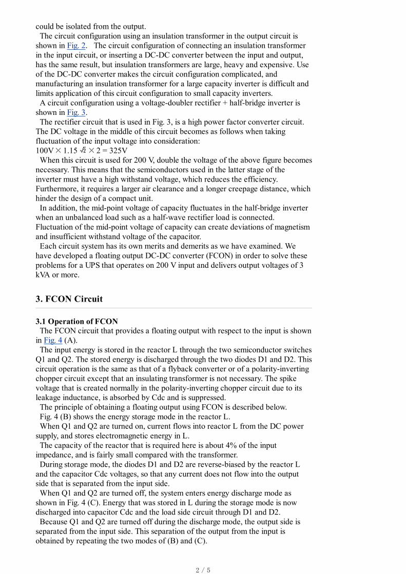
could be isolated from the output.
The circuit configuration using an insulation transformer in the output circuit is
shown in Fig. 2. The circuit configuration of connecting an insulation transformer
in the input circuit, or inserting a DC-DC converter between the input and output,
has the same result, but insulation transformers are large, heavy and expensive. Use
of the DC-DC converter makes the circuit configuration complicated, and
manufacturing an insulation transformer for a large capacity inverter is difficult and
limits application of this circuit configuration to small capacity inverters.
A circuit configuration using a voltage-doubler rectifier + half-bridge inverter is
shown in Fig. 3.
The rectifier circuit that is used in Fig. 3, is a high power factor converter circuit.
The DC voltage in the middle of this circuit becomes as follows when taking
fluctuation of the input voltage into consideration:
100V 1.15 2 = 325V
When this circuit is used for 200 V, double the voltage of the above figure becomes
necessary. This means that the semiconductors used in the latter stage of the
inverter must have a high withstand voltage, which reduces the efficiency.
Furthermore, it requires a larger air clearance and a longer creepage distance, which
hinder the design of a compact unit.
In addition, the mid-point voltage of capacity fluctuates in the half-bridge inverter
when an unbalanced load such as a half-wave rectifier load is connected.
Fluctuation of the mid-point voltage of capacity can create deviations of magnetism
and insufficient withstand voltage of the capacitor.
Each circuit system has its own merits and demerits as we have examined. We
have developed a floating output DC-DC converter (FCON) in order to solve these
problems for a UPS that operates on 200 V input and delivers output voltages of 3
kVA or more.
3. FCON Circuit
3.1 Operation of FCON
The FCON circuit that provides a floating output with respect to the input is shown
in Fig. 4 (A).
The input energy is stored in the reactor L through the two semiconductor switches
Q1 and Q2. The stored energy is discharged through the two diodes D1 and D2. This
circuit operation is the same as that of a flyback converter or of a polarity-inverting
chopper circuit except that an insulating transformer is not necessary. The spike
voltage that is created normally in the polarity-inverting chopper circuit due to its
leakage inductance, is absorbed by Cdc and is suppressed.
The principle of obtaining a floating output using FCON is described below.
Fig. 4 (B) shows the energy storage mode in the reactor L.
When Q1 and Q2 are turned on, current flows into reactor L from the DC power
supply, and stores electromagnetic energy in L.
The capacity of the reactor that is required here is about 4% of the input
impedance, and is fairly small compared with the transformer.
During storage mode, the diodes D1 and D2 are reverse-biased by the reactor L
and the capacitor Cdc voltages, so that any current does not flow into the output
side that is separated from the input side.
When Q1 and Q2 are turned off, the system enters energy discharge mode as
shown in Fig. 4 (C). Energy that was stored in L during the storage mode is now
discharged into capacitor Cdc and the load side circuit through D1 and D2.
Because Q1 and Q2 are turned off during the discharge mode, the output side is
separated from the input side. This separation of the output from the input is
obtained by repeating the two modes of (B) and (C).
2 / 5
The current patterns of the respective semiconductor devices constituting the
circuit are shown in Fig. 4 (D). Current Iq of Q1 and Q2, and current Id of D1 and
D2 increase and decrease with the following slopes.
(1)
(2)
The relationship between the switching duty ratio D of Q1 and Q2, and the output
voltage can be expressed by the following equations assuming that voltage drop due
to semiconductor devices is 0 and assuming that the resistive component is 0.
(3)
(4)
The relationship between the input/output and duty ratio is shown in Fig. 4 (E).
The input voltage can be stepped up or down by changing the duty as shown in Fig.
4 (E). However, non-linearity increases and controllability deteriorates when the
duty ratio exceeds 0.5.
3.2 Limitations of FCON
The single winding reactor that is used in FCON can be easily manufactured
because it does not have the leakage inductance problem, and so should be useful
for large-capacity systems.
However, the conversion to the floating output of FCON has a limitation compared
with the transformer that is a passive component. The floating output of FCON is
obtained by switching the semiconductor switch and diode in a time-shared manner.
Among the switching elements, the diode turns on depending on external
conditions because it is a passive element even during the period in which it must be
turned off. In other words, it can create a mode in which the input and output are
directly connected, thus losing the separation of input from output that is required
for floating output.
The conditions that are inhibited during use of FCON are shown in Fig. 5.
When external voltage Ex is applied as shown in Fig. 5, diode D1 conducts when
IGBT or FET or transistor is used for switch Q1 because it cannot prevent the
circuit from reverse voltage.
In the same manner, when voltage Ey is applied, diode D2 conducts so that the
input and output circuits are directly connected and floating output cannot be
obtained. When a snubber circuit or equivalent is connected in parallel with Q1 and
Q2, or D1 and D2, the input and output circuits are connected through it. The
structure of the snubber must be considered carefully.
4. Application of FCON to UPS
4.1 Structure of Rectifier Circuit
FCON is equipped with a floating output that is necessary for the UPS rectifier as
described in Chapters 2 and 3. No rush current suppression circuit is necessary
because the rush current to capacitor Cdc during start-up can be suppressed by
implementing soft-start of the semiconductor switches Q1 and Q2 that are used to
3 / 5

separate the input side. At the same time, because the fundamental operation of this
circuit is that of a flyback converter, this circuit can be operated as a high power
factor converter by comparing the current flowing through the reactor L with the
input voltage as reference voltage, and by controlling the current flowing through L
into a sine wave current.
The circuit structure as a high power factor converter is shown in Fig. 6
The characteristics as a high power factor converter are, from the above circuit,
Input power factor: 99.3% when input and output powers are rated power, and
Conversion efficiency: 88.4% when input and output powers are rated power.
Fig. 7 Waveforms at key circuits when FCON is used as a high power factor
converter
4.2 UPS using FCON
The structure of the UPS using FCON is shown in Fig. 8.
The output voltage of the rectifier circuit as described in section 4.1, is sent to the
inverter consisting of a full bridge structure, and the inverter outputs a sine wave
AC voltage of constant frequency and constant voltage. This output is floating from
the input of the UPS by FCON.
LO and CO that are connected to the AC input circuit constitute a filter that
suppresses ripples caused by switching of semiconductor switches Q1 and Q2, and
absorbs high frequency noise.
The AC filter forms a circuit that connects the DC bus and the AC output terminal
with a capacitor. This assures the reverse bias voltage of the diode D1 and D2 which
prevents leakage of noise into this circuit.
The neutral line of the AC input power supply and one of the output lines are
connected in common. This connection solves the problems related to earth as
described in Chapter 2.
The next section considers whether the common connection line as described
above causes any problems for the FCON operation.
An unnecessary forward bias must not be applied to the diode for the correct
functioning of FCON as described before. The bias status of the diode is explained
by the bias modes of the FCON diodes in Fig. 9.
Figs. 9 (A) and (B) illustrate the bias status of diode D1. In the mode shown in Fig.
9 (A), the voltage across AC filter capacitor C1 is applied to D1 as a reverse bias via
the input/output connection line. This connection cannot work as a forward bias. In
the mode shown in Fig. 9 (B), the sum of voltages across AC filter capacitor C0 and
C2 is applied to D1 as a reverse bias. The modes shown in Figs. 9 (C) and (D) are
the bias mode for diode D2. In the mode shown in Fig. 9 (C), the sum of the
voltages across C0 and C2 are applied as a reverse bias. In the mode shown in Fig. 9
(D), the C2 voltage is applied as a reverse bias.
As explained above, diodes D1 and D2 cannot be forward-biased while the main
power is on. This allows the FCON UPS to deliver its full performance.
The newly developed 3 kVA UPS and the conventional 3 kVA UPS are compared
below.
Contents New UPS Conventional UPS
Volume 51 liters 101 liters
Mass 75 kg 125 kg
Input power factor 99.3 % 99 %
Input voltage range 170 V to 265 V 176 V to 224 V
Overall efficiency 84.3 % 78.9 %
Noise specification VCCI approved Conforms to VCCI
4 / 5
Note: The conventional UPS is the ASH30 input/output 200 V type.
5. Conclusion
We have verified the floating output DC-DC converter (FCON) using a single
winding reactor with a UPS. The floating output DC-DC converter is a high power
factor converter and is used as the rectifier circuit of a UPS of single-phase, 200 V, 2
kVA output.
The floating output DC-DC converter with single winding reactor has the following
features:
(1) Because FCON uses a single winding reactor to obtain the floating output, the
DC-DC converter is easy to manufacture, and an inverter having a large power
conversion capacity can be manufactured.
(2) Because FCON can be stepped up and down, an inverter having a wide range of
input voltage deviations is realized.
(3) Because the conventional inverter uses a transformer, equipment is large and
heavy. The new inverter is compact and light.
(4) Transformers running at commercial frequency are expensive. Since the
transformer is no longer needed, the cost of the new inverter is lower.
We intend to apply this new technology to three-phase circuits, increase the
efficiency, and so on in future. Further development of this technology will be based
on its unique characteristics.
References
(1) Sekino, Yamazaki: "Floating Output DC-DC Converter Using Single Winding
Reactor". The Institute of Electronics, Information and Communication
Engineers Technical Report, EE98-1 (1998-6)
Hirohisa Yamazaki
Joined company in 1974
Power Systems Division, 2nd Design Dept.
Worked on design and development of small capacity UPS
5 / 5
Fig. 1 Full wave rectification + full bridge inverter
1 / 1
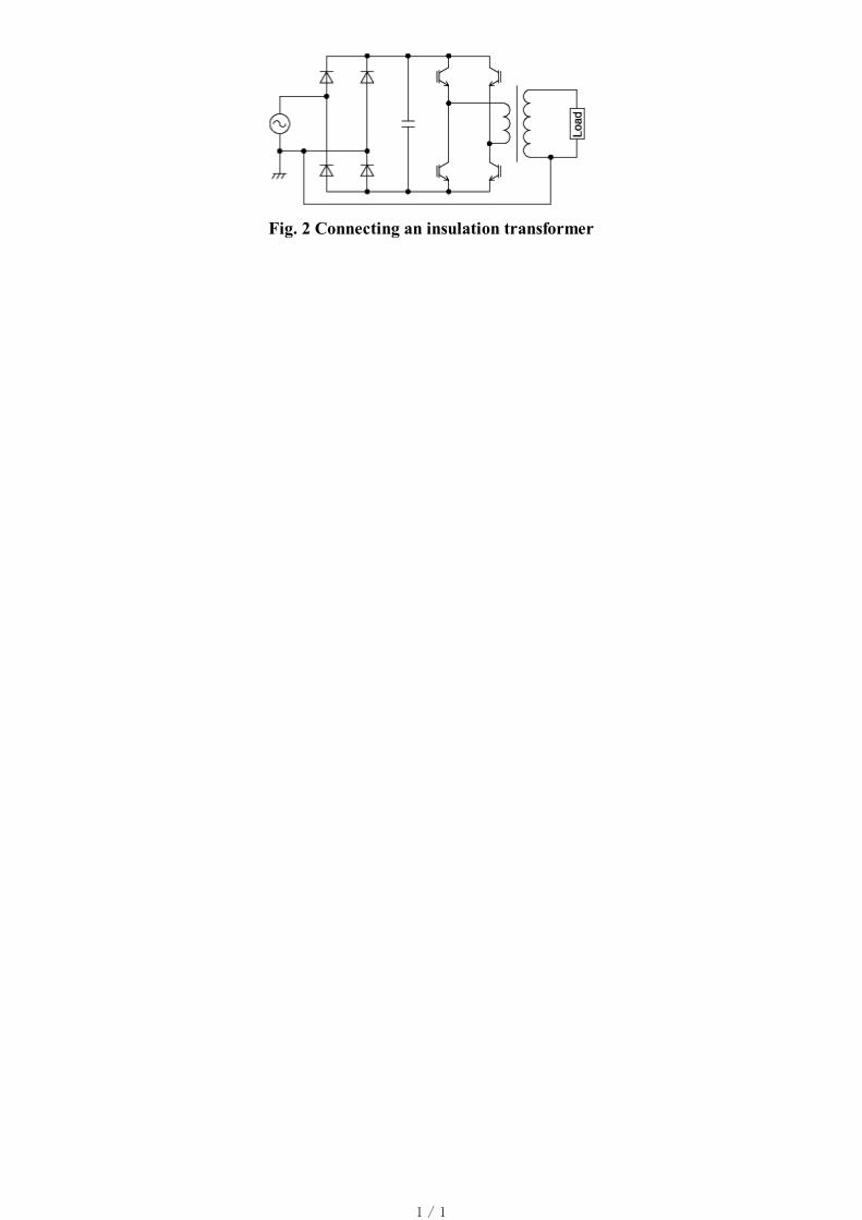
Fig. 2 Connecting an insulation transformer
1 / 1
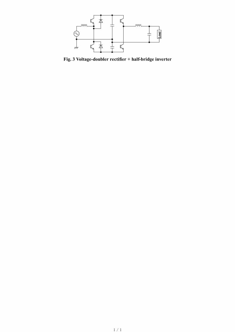
Fig. 3 Voltage-doubler rectifier + half-bridge inverter
1 / 1
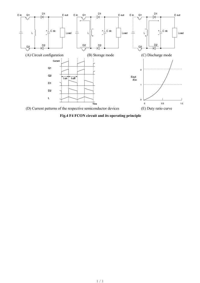
(A) Circuit configuration (B) Storage mode (C) Discharge mode
(D) Current patterns of the respective semiconductor devices (E) Duty ratio curve
Fig.4 F4 FCON circuit and its operating principle
1 / 1
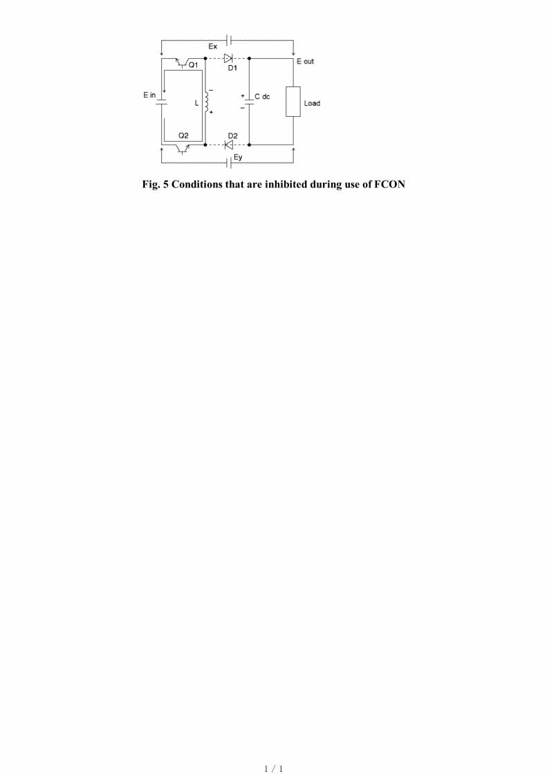
Fig. 5 Conditions that are inhibited during use of FCON
1 / 1

(A) Main circuit structure (B) Structure of control circuit
(C) Description of operation
Fig. 6 Circuit structure as a high power factor converter
1 / 1
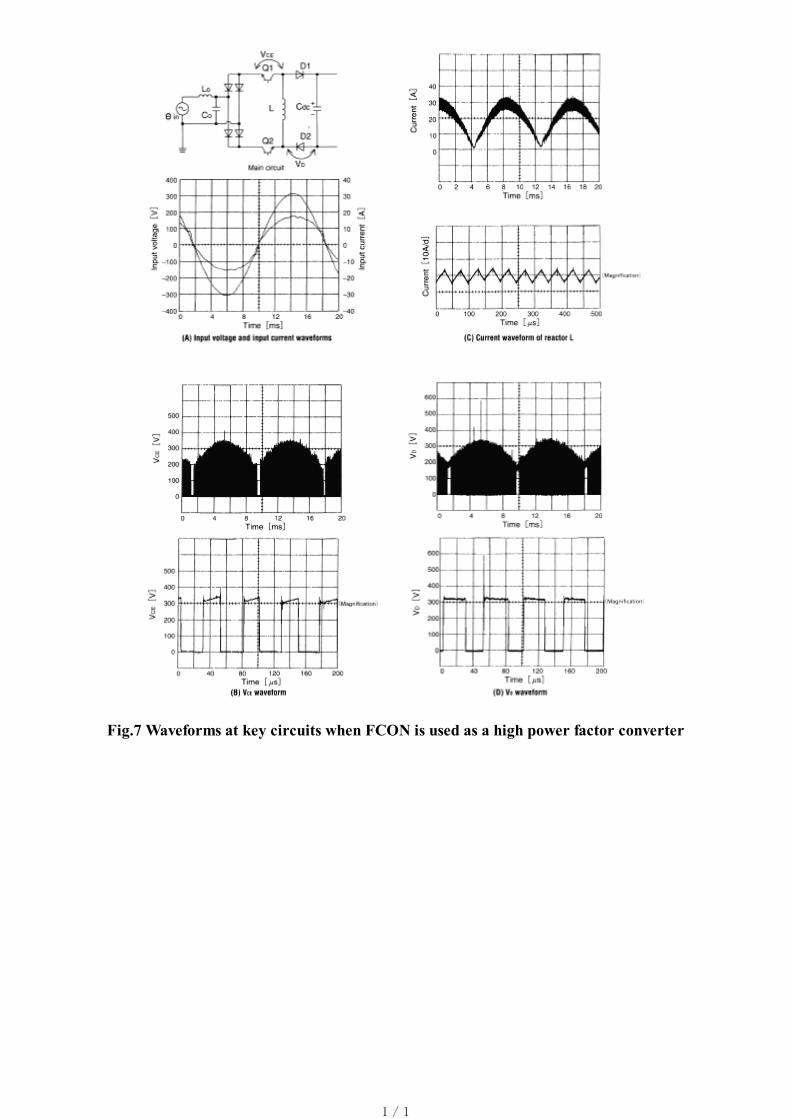
Fig.7 Waveforms at key circuits when FCON is used as a high power factor converter
1 / 1
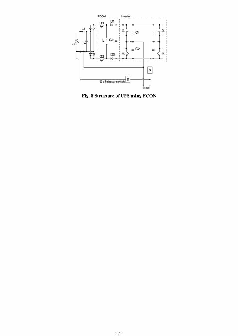
Fig. 8 Structure of UPS using FCON
1 / 1
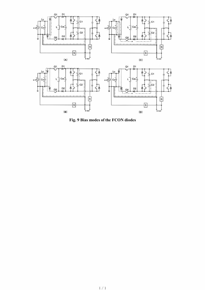
Fig. 9 Bias modes of the FCON diodes
1 / 1