folded cascode amplifier - woodworth...
TRANSCRIPT

Folded Cascode Amplifier Final Project Report
By: Kyle Woodworth
ECE59500 December 14, 2015

KW595 Design Overview Amplifiers tend to have a wide variety of usage depending on their specifications. In
other words, there are a lot of ways to design an amplifier and optimize it for a specific
application. I will be targeting a single supply, lowpower folded cascode amplifier with high gain
and bandwidth. There are two applications which will be implemented that use this design. The
first application will be a first order active filter. The second application will be a switched
capacitor filter. However, these are not the only applications, just two that will be implemented to
ensure a deeper understanding of the design process of an integrated amplifier. Other
applications can include analog to digital converter, digital to analog converter, circuit isolation,
buffers, drivers, etc.
Table 1 shows the initial project proposal specifications as well as modified
specifications after feedback was provided for the proposal. Some important parameters were
not included in the project proposal like input noise, input common mode range, and output
swing range. I also added a specification for settling time. The initial specifications were chosen
by analyzing datasheets of commercial opamps that had similar applications to my target
application. The modified specifications were chosen based off of the initial specifications and
feedback provided.
Figure 1 shows the final architecture of the KW595 folded cascode amplifier. Transistors
M0 and M1 act as the differential input stage with M3 acting as the current source for the input
transistors to have an AC ground. A current mirror is created from transistor M4 with a 25μA
current source created through a 105kΩ resistor. Transistors M14, M19, M21, and M23 are the
cascode amplifying branch for the noninverted input. This branch current is mirrored to the
inverting cascode branch. The inverting cascode branch is made up of transistors M15, M18,

M22, M24. The output voltage is taken at the node where M18’s drain is connected to M24’s
drain. Calculation of the sizing and biasing currents of each transistors is explained later in the
report.
Parameter Initial Specification Modified Specification
Technology TSMC 0.25 nm Technology TSMC 0.20 nm Technology
OpenLoop Gain 200 V/mV 70 dB
Unity Gain Bandwidth 100 MHz 100 MHz
Slew Rate 60 V/μs 60 V/μs
Settling Time 10 ns
Supply Voltage 3.35 V 3.3 V
Supply Current < 1.5 mA < 1.5 mA
Offset Voltage +/ 5 mV +/ 5 mV
CMRR 100 dB 80 dB
PSRR 75 dB 75 dB
Input Impedance 5 MΩ 5 MΩ
Input Noise
Input CM Range
Output Swing Range 0.5V to 2.5V
Table 1 Initial performance specifications of the KW595 design

Figure 1 Architecture of the KW595

Design Calculations The gain of a folded cascode amplifier can be determine through a quick analysis. We
first notice that the input is just a CS stage. The next thing is that the output of the CS stage is
folded into a cascode branch. The gain of a folded cascode branch can be estimated through
the following equation:
[− (r //r )][g (r g r )]Av = gm1 o1 o5 m2 o3 m3 o4
Where M1 is the input stage, M5 is a PMOS current source, M2 is the PMOS current
buffer, and M3 and M4 is the cascode current source. Now we need to figure out what the
transconductance and output resistances of these transistors should be. The transconductance
is given through the following equations:
gm = 2IDV −VGS TH
We can see that the transconductance is dependent on the bias condition of the
transistor. The output resistance is similar:
(λI )ro = D−1
The output resistance is dependent on the bias current and proportional to the length of
the transistor since . λ ~ L−1
Now we have set of equations that can help us determine the some of the parameters of
the opamp. The final question how to determine the biasing condition of each transistor. This is
really the design process. Since I want my supply current to be less than 1.5 mA I will allocate
25μA for the current mirror and 4μA to each cascode branch and the differential current branch.
Since the output voltage swing needs to be from 0.5V to 2.5V I will allocate the overdrive
voltage to M21, M22, M23, and M24 to 0.25V. Leaving the lower threshold of the output swing
to 0.5V. The current buffers M18 and M19 I will allocate 0.3V. Since since M14 and M15 will be

supplying more current, I will allocate a 0.5V overdrive voltage. This leaves the upper limit of the
output swing to 2.5V. We have decided on the biasing condition for most of the transistors, now
I need an equation to find the aspect ratio. From the IV characteristic equation of a MOSFET
we can determine that:
W /L) ( = 2IDμC Vox OD
2
That seems like it’ll work! Now through the magic of python I have been given the
following parameters for each transistor shown in Table 2. Using table 2 we can estimate the
gain of the amplifier to be: 33333 V/V which is about 90 dB. This is well above the performance
specification. The table also says the output resistance of the opamp will be 165 MΩ.
Transistors Transconductance Output Resistance Aspect Ratio
M0 M2 1e5 A/V 5 MΩ 11.03
M14 M15 3.2e5 1.25 MΩ 63.75
M18 M19 2e5 A/V 2.5 MΩ 49.8
M2124 2.67e5 A/V 2.5 MΩ 39.23
Table 2 Calculated transistor parameters

Gain and Phase Margin
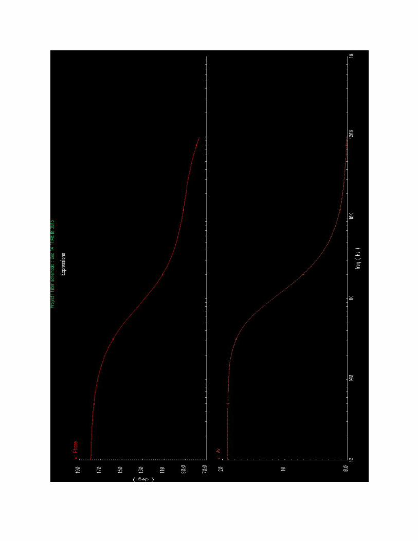
Figure 2 Gain and Phase Performance
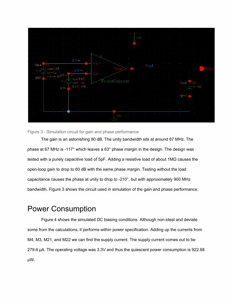
Figure 3 Simulation circuit for gain and phase performance
The gain is an astonishing 80 dB. The unity bandwidth sits at around 67 MHz. The
phase at 67 MHz is 117° which leaves a 63° phase margin in the design. The design was
tested with a purely capacitive load of 5pF. Adding a resistive load of about 1MΩ causes the
openloop gain to drop to 60 dB with the same phase margin. Testing without the load
capacitance causes the phase at unity to drop to 210°, but with approximately 900 MHz
bandwidth. Figure 3 shows the circuit used in simulation of the gain and phase performance.
Power Consumption Figure 4 shows the simulated DC biasing conditions. Although nonideal and deviate
some from the calculations, it performs within power specification. Adding up the currents from
M4, M3, M21, and M22 we can find the supply current. The supply current comes out to be
279.6 μA. The operating voltage was 3.3V and thus the quiescent power consumption is 922.68
μW.
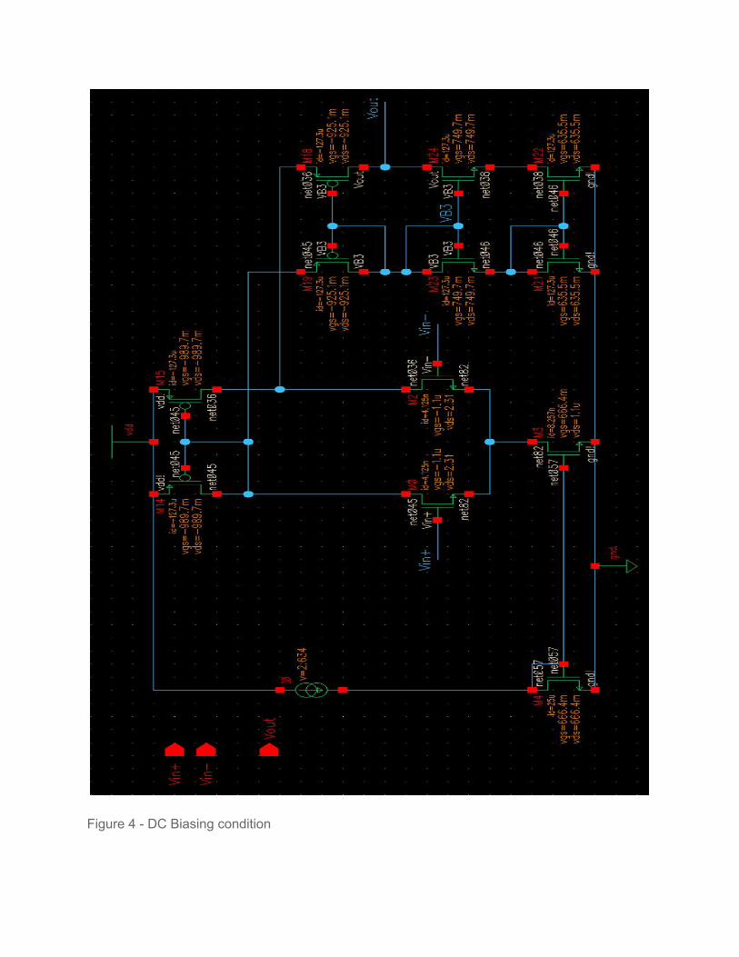
Figure 4 DC Biasing condition

Input Characteristics From my understanding the input offset voltage is due to mismatched transistors from
the nonidealities of the real world. Therefore, I was not able to test the input offset voltage of
the design. The input impedance is ideally infinite which would mean no current is drawn into
the design. Simulating a simple voltage follower configuration with the design, it can be seen
that no current is drawn.
Rejection Ratios The commonmode rejection ratio is how resilient the output is as the commonmode
voltage changes. Figure 5 shows the resulting CMRR bode plot and Figure 6 shows the test
circuit used to simulate the CMRR. The CMRR is given through the following equation:
CMRR| | = AVACM = voutvCM
The powersupply rejection ratio is how resilient the output is as the powersupply
changes. Figure 7 shows the resulting PSRR bode plot and Figure 8 shows the test circuit used
to simulate the PSRR. The PSRR simulation circuit is just a voltage follower, but the vdd! net
has been modified to include some AC magnitude. The PSRR is given through the following
equation where is the gain from the powersupply variation.Add
SRR P = AVAdd

Figure 5 CMRR Bode Plot
Figure 6 CMRR Simulation Circuit

Figure 7 PSRR Bode Plot
Figure 8 PSRR Simulation Circuit (Note the noise is defined when vdd is defined for simulation)

Output Characteristics The calculated output impedance was said to be around 165 MΩ. The overdrive voltages
for transistors were chosen to allow for the appropriate range of output swing. Sweeping a DC
voltage at the noninverting input from 0 to 3.3V and monitoring the output voltage will allow us
to get a good feel for the output voltage of the design. Figure 9 shows that the output swing
goes from 0.323V to 2.53V.
Figure 9 Output Swing Range

Slew Rate and Settling Time Figure 10 shows the step response of the design in a voltage follower configuration. It
can be seen that the slew rate (slope of the step response) is about 3 V/ns. The settling time is
the time taken to go from 2V to 2.5V at the top of the step response.
Figure 10 Slew Rate and Settling Time step response analysis

Cascode Amplifier Results
Parameter Project Specification Simulation Result
OpenLoop Gain 70 dB 80 dB
Unity Gain Bandwidth 100 MHz 65 MHz
Slew Rate 60 V/μs 3 V/ns
Settling Time 10 ns 3.5 ns
Supply Voltage 3.3V 3.3 V
Supply Current < 1.5 mA 279.6 uA
Input Offset Voltage +/ 5 mV 0.323V
CMRR 100 dB 65 dB
PSRR 75 dB 22.8 dB
Input Impedance 5 MΩ 165 MΩ
Input CM Range 0.8 V to 1.8 V
Output Swing Range 0.5V to 2.5V 0.323V to 2.53V
Table 3 Simulation and Proposed Specifications

Continuous Time First Order LowPass Filter
Calculations
For the continuous time domain lowpass filter I am aiming for a gain of 20 V/V with a 3
dB corner frequency at 5 kHz. In order to achieve a gain of 20 V/V I chose to use a 10 kΩ as
the input resistor and 200kΩ as the feedback resistor using the following equation.
vinvout = − R1
RF
Where is the feedback resistance and is the input resistance that converts theRF R1
input signal into current. This will yield a 20 V/V gain. In order to get the corner frequency to 5
kHz I used a 1 nF feedback capacitor using the following equation.
f3dB = 1R CF F
Where is the feedback resistance and is the feedback capacitance.RF CF
Testing Scenario
The simulation circuit is shown below. The input is assumed to be a 20 μVpp sinusoidal
wave. The input common mode is set to be 1.5 V and is simulated with an ideal voltage source.
The load is assumed to be a 5 pF capacitor and a 165 MΩ resistor.

Results and Graphs
Parameter Calculation Simulation
Gain 20 V/V 19.14 V/V
Corner Frequency 5 kHz 7.5 kHz

Discrete Time First Order LowPass Filter
Calculations
Working from the calculations of the CTD LPF, we can transform the resistors into a
combination of MOSFETs and capacitors to convert the LPF into a discrete time domain LPF.
Using the following equation we can produce an equivalent resistance for a switched capacitor
network.
Req = 1f CCK s
Where is the frequency of the clock that is controlling the sampling and is thefCK Cs
sampling capacitance. Using this equation I am replacing the 10 kΩ input resistor with two
clocked MOSFETs and a 100 pF sampling capacitor. Likewise, the 200 kΩ gets converted into
two MOSFETs and a 5 pF sampling capacitor.
Testing Scenario
The simulation circuit is shown below. The input is assumed to be a 20 μVpp sinusoidal
wave. The input common mode is set to be 1.5 V and is simulated with an ideal voltage source.
The load is assumed to be a 10 nF capacitor to filter out the high frequency sampling in order to
achieve a smoother output signal. The clock is assumed to be a 1 MHz, 5 V square wave with a
1 ps rise and fall time.


Results and Graphs
The graph below is a plot of the DTD LPF frequency response. The gain is around 17.5 for very low frequencies, which is close to the target gain, but seems to drop off faster, however the corner frequency seems to hold up well.
Parameter Calculation Simulation
Gain 20 V/V 9.025 V/V
Corner Frequency 5 kHz 7.5 kHz