for information equipment mn5515 - panasonic · for information equipment mn5515 ... ss nwe nre bnw...
TRANSCRIPT
For Information Equipment
MN5515High-Speed Color Conversion LSI
OverviewThe MN5515 is a high-speed color conversion processor
capable of free conversion among various full-color formats.It offers a low-cost solution to reproducing colors from
various sources in multimedia environments.Note: This product is manufactured under license from Electron-
ics for Imaging, Inc., holders of US Patent 4,837,722.
FeaturesConformable to ICC standard model
Real-time conversion of full-color signals using prisminterpolation method
Greater precision in reproducing black with new slantprism interpolation method
An appropriate management for the system is availableby only setting the three-dimensional look-up table inRAM that attaches to the host interface.
Maximum processing speed (tmin): 62.5 ns/pixel
Maximum operating frequency (fmax): 16 MHz
Data width for pixel input: 8 bits × 3 channels
ApplicationsFaithful color reproduction with color scanners, colorprinters, color copiers, color facsimile machines, andother office electronics equipment
Color adjustment for television cameras, displays, andother imaging equipment
High-speed accelerator in color conversion for com-puter graphics, computer-aided design, and workstationapplications
Differentiating parts by color on automated productionlines
Data width for pixel output: 8 bits × 1 channel
Host interface bus width: 8 or 10 bits(Switchable at any time during operation)
Number of memories of 3D-LUT:9 × 9 × 9 = 729
Color conversion look-up table output datawidth (signed): 10 bits
Choice of built-in prism or slant prisminterpolation funciton by a register
Auxiliary delay line: 1 bit (10 t pipeline delay)
Pipeline delay: 10 t (t: 1 GCLK)
Mainten
ance/
Discon
tinued
Mainten
ance/D
iscont
inued
includ
es foll
owing
four P
roduct
lifecyc
le stag
e.
(planed
mainten
ance ty
pe, main
tenanc
e type,
planed
discon
tinued
typed,
discon
tinued
type)
MN5515 For Information Equipment
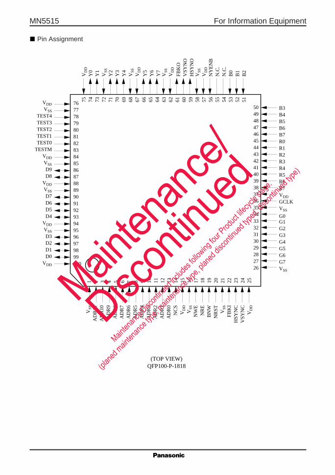
Pin Assignment
VDDVSS
TEST4TEST3TEST2TEST1TEST0
TESTMVDDVSSD9D8
VDDVSSD7D6D5D4
VDDVSSD3D2D1D0
VDD
767778798081828384858687888990919293949596979899100
50494847464544434241403938373635343332313029282726
B3B4B5B6B7R0R1R2R3R4R5R6R7VDDGCLKVSS
G0G1G2G3G4G5G6G7VSS
VSS
AD
R11
AD
R10
AD
R9
AD
R8
AD
R7
AD
R6
AD
R5
AD
R4
AD
R3
AD
R2
AD
R1
AD
R0
NC
SV
DD
VSS
NW
EN
RE
BN
WN
RST VSS
FBK
IH
SYN
CV
SYN
CV
DD
1 2 3 4 5 6 7 8 9 10 11 12 13 14 15 16 17 18 19 20 21 22 23 24 25
75 74 73 72 71 70 69 68 67 66 65 64 63 62 61 60 59 58 57 56 55 54 53 52 51
VD
DY
0Y
1V
SSY
2Y
3Y
4V
SSV
DD
Y5
Y6
Y7
VSS
VD
D
FBK
OV
SYN
OH
SYN
OV
SSV
DD
NY
EN
BN
.C.
N.C
.B
0B
1B
2
(TOP VIEW)QFP100-P-1818
Mainten
ance/
Discon
tinued
Mainten
ance/D
iscont
inued
includ
es foll
owing
four P
roduct
lifecyc
le stag
e.
(planed
mainten
ance ty
pe, main
tenanc
e type,
planed
discon
tinued
typed,
discon
tinued
type)
For Information Equipment MN5515
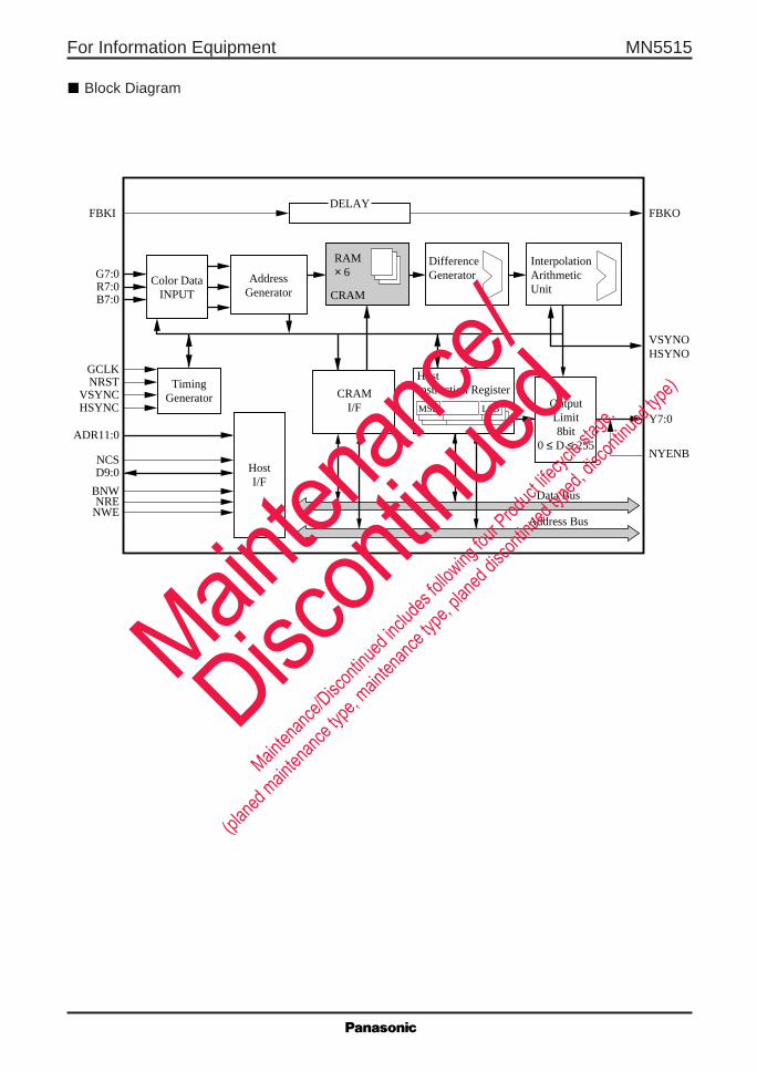
Block Diagram
R7:0G7:0
B7:0
NCS
ADR11:0
D9:0
BNWNRE
NWE
NRSTGCLK
VSYNCHSYNC
TimingGenerator
HostI/F
Color DataINPUT
AddressGenerator
CRAMI/F
DELAY
DifferenceGenerator
RAM× 6
CRAM
Interpolation ArithmeticUnit
HostInstruction Register
OutputLimit8bit
0 ≤ D ≤ 255
Y7:0
VSYNOHSYNO
FBKOFBKI
NYENB
Data Bus
Address Bus
MSB LSB
Mainten
ance/
Discon
tinued
Mainten
ance/D
iscont
inued
includ
es foll
owing
four P
roduct
lifecyc
le stag
e.
(planed
mainten
ance ty
pe, main
tenanc
e type,
planed
discon
tinued
typed,
discon
tinued
type)

MN5515 For Information Equipment
Pin Descriptions
Pin No. Symbol Type I/O Number Level Logic Function description Remarks
14 NCS Control I 1 T L Chip select
18 NRE signals I 1 T L Read enable
17 NWE I 1 T L Write enable
2 to 13 ADR11 to 0 I 12 T H Address bus
86, 87, D9 to 0 I/O 10 T H Bidirectional data bus
90 to 93,
96 to 99
20 NRST I 1 T L System reset
19 BNW I 1 T Byte/word select H/L: Byte/word
56 NYENB I 1 T L Image output enable
36 GCLK Image I 1 T H Pixel clock
27 to 34 G7 to 0 I/O I 8 T H Pixel input (G)
38 to 45 R7 to 0 signals I 8 T H Pixel input (R)
46 to 53 B7 to 0 I 8 T H Pixel input (B)
64 to 66 , Y7 to 0 O 8 T H Color conversion
69 to 71 , output data
73 , 74
24 VSYNC I 1 T L Vertical synchroniza-
tion signal
23 HSYNC I 1 T L Horizontal synchroni-
zation signal
60 VSYNO O 1 T L Vertical delay VSYNC output
synchronization signal
59 HSYNO O 1 T L Horizontal delay HSYNC output
synchronization signal
22 FBKI I 1 T Auxiliary input signal
61 FBKO O 1 T Auxiliary output signal
78 to 82 TEST4 to 0 Miscel- I 5 T Test signal Connect these to ground
83 TESTM laneous I 1 C Test signal Connect this to ground
15 , 25 , VDD Power I +5V Connect all pins.
37 , 57 , supply
62 , 67 ,
75 , 76 ,
84 , 88 ,
94 , 100
1 , 16 , VSS I 0V Connect all pins.
21 , 26 ,
35 , 58 ,
63 , 68 ,
72 , 77,
85 , 89 ,
95T: TTL C: CMOS H: High L: Low
Mainten
ance/
Discon
tinued
Mainten
ance/D
iscont
inued
includ
es foll
owing
four P
roduct
lifecyc
le stag
e.
(planed
mainten
ance ty
pe, main
tenanc
e type,
planed
discon
tinued
typed,
discon
tinued
type)

For Information Equipment MN5515
Functional Description
Color conversion algorithmThis color conversion LSI converts colors using a three-dimensional look-up table and three-dimensional
interpolation.The three-dimensional look-up table holds output values at representative pixel-input. The number of represen-
tative output points in the operating mode is shown in the following table.
Number of Representative Points in Three-Dimensional Look-Up Table
Prism Interpolation Slant Prism Interpolation
333 mode 9 × 9 × 9 = 7299 × 9 × 9 = 729 (MN5515 configuration)
11 × 11 × 9 = 1089 (if lattice points extrapolation does not used)
For slant prism interpolation, the MN5515 uses the same 729 points that it uses for prism interpolation so as tosupport lattice point extrapolation. It derives its output image data with three-dimensional interpolation based onthe data for the six lattice points by prism or slant prism interpolation method that depends on the input imagedata.
1. Prism interpolation methodFigure 1 illustrates the procedure that the color conversion LSI applies to produce prism interpolation.
a b
e
cd
h
f
ga
b, (d)
c
e
f, (h)
g
Data for six lattice points
Three-dimensional look-up table
Input signal
Three-dimensional interpolation
Green
Red
Blue
Output signal
Green, red, blueG
B
R
G
B
R
Figure 1 Principle of Operation for Color Conversion LSI
Mainten
ance/
Discon
tinued
Mainten
ance/D
iscont
inued
includ
es foll
owing
four P
roduct
lifecyc
le stag
e.
(planed
mainten
ance ty
pe, main
tenanc
e type,
planed
discon
tinued
typed,
discon
tinued
type)

MN5515 For Information Equipment
Figure 2 illustrates the prism interpolation algorithm itself. Point o represents the position of the input data inthe coordinate space; points a, b, c, e, f, and g, the six lattices points specified by the upper bits in the data; D(a),D(b), D(c), D(e), D(f), and D(g), the data values for these lattice points. The line mn is the perpendicular joiningthe two parallel prism faces and passing through point o. The output data D(o) is derived from the following linearinterpolation calculation with weighting coefficients based on these 6 data and the lower bits of the input data.
If RL ≥ BLD(o)=D(m)+(D(n)–D(m))GL/L (Note: L is a unit distance between lattice points)where,D(m)=D(a)+(D(b)–D(a))RL/L+(D(c)–D(b))BL/LD(n)=D(e)+(D(f)–D(e))RL/L+(D(g)–D(f))BL/L
If RL < BLD(o)=D(m)+(D(n)–D(m))GL/Lwhere,D(m)=D(a)+(D(c)–D(d))RL/L+(D(d)–D(a))BL/LD(n)=D(e)+(D(g)–D(h))RL/L+(D(h)–D(e))BL/L
2. Slant prism interpolation methodFigure 3 illustrates the procedure that the color conversion LSI applies to produce slant prism interpolation.
aa
e
e
d
h
c
c
f
g
g
RLBL
GL
b
m
o
n
a
e
b
fc
gPrism0 (RL ≥ BL) Prism1 (RL < BL)
Figure 2 Prism Interpolation Algorithm
Figure 3 Principle of Color Conversion LSI Operation
a RL-GLBL-GL
b
m
GL
e
c
nf
ga
b, (d)
c
e
f, (h)
g
Data for six lattice points
Green
Red
Blue
Output signal
Green, red, blue
G B
R
G
B
R
Input signal
Three-dimensional look-up table Slant prism interpolation
Mainten
ance/
Discon
tinued
Mainten
ance/D
iscont
inued
includ
es foll
owing
four P
roduct
lifecyc
le stag
e.
(planed
mainten
ance ty
pe, main
tenanc
e type,
planed
discon
tinued
typed,
discon
tinued
type)

For Information Equipment MN5515
Figure 4 illustrates the slant prism interpolation algorithm itself. Point o represents the position of the input datain the coordinate space; points a, b, c, e, f, and g, the six lattices points specified by the upper bits in the data; D(a),D(b), D(c), D(e), D(f), and D(g), the output values for these lattice points. The line mn is parallel to the slant-prism axis (a–e) and passing through point o. The output data D(o) is derived from the following linear interpola-tion calculation with weighting coefficients based on these 6 data and the lower bits of the input data.
If (RL–GL) ≥ (BL–GL)D(o)=D(m)+(D(n)–D(m))GL/L (Note: L is the lattice spacing)where,D(m)=D(a)+(D(b)–D(a))(RL–GL)/L+(D(c)–D(b))(BL–GL)/LD(n)=D(e)+(D(f)–D(e))(RL–GL)/L+(D(g)–D(f))(BL–GL)/L
If (RL–GL) < (BL–GL)D(o)=D(m)+(D(n)–D(m))GL/Lwhere,D(m)=D(a)+(D(c)–D(d))(RL–GL)/L+(D(d)–D(a))(BL–GL)/LD(n)=D(e)+(D(g)–D(h))(RL–GL)/L+(D(h)–D(e))(BL–GL)/L
If (RL-GL), (BL-GL) in the above derivation is negative, anticipated origin correction automatically ensuresthat they are positive by adding L: (RL-GL)+L, (BL-GL)+L.
a RL-GL
BL-GL
b
m
GL
o
e
e
c
c Prism1 (RL-GL < BL-GL)
Prism0 (RL-GL ≥ BL-GL)
n
f
g
gh
d
aa b
e
c
f
g
Figure 4 Slant Prism Interpolation Algorithm
Mainten
ance/
Discon
tinued
Mainten
ance/D
iscont
inued
includ
es foll
owing
four P
roduct
lifecyc
le stag
e.
(planed
mainten
ance ty
pe, main
tenanc
e type,
planed
discon
tinued
typed,
discon
tinued
type)

MN5515 For Information Equipment
3. Interpolation precisionThe MN5515 uses signed integer arithmetic for all internal processing. The entries in the color conversion table
are signed 10-bit integers (–512 to 511); the weighting coefficients for interpolation, unsigned 5-bit integers (0 to31). To minimize rounding errors during internal processing and reduce arithmetic errors in the output, the LSIuses enhanced bit for internal arithmetic.
The following table gives the error, δ, between the output value and the calculated value for the each modes ofthe MN5515.
Error, δ, between Output Value and Calculated Value for Color Conversion LSI
Output Magnification of 1 Output Magnification of 1/2 Output Magnification of 1/4
Half compression mode –1LSB ≤ δ ≤ 0 –1LSB ≤ δ ≤ 0 –1LSB ≤ δ ≤ 0
Standard mode –1LSB ≤ δ ≤ 0 –1LSB ≤ δ ≤ 0 –1LSB ≤ δ ≤ 0
4. Internal structure of three-dimensional look-up tableThe three-dimensional look-up table is stored in six RAM chips (CRAM: M0 to M5). The following formulas
derive CRAM number, Mi, and byte address, Ai, from the three-dimensional look-up table indices, Xi, Yi, and Zi.
Mi=(Xi+Yi)%3+(Zi%2) × 3Ai=Xi/3+Yi × C1+(Zi/2) × C2 × 2
Note: The Xi/3 indicate integer division discarding any remainder.
The percent signs indicate the modulo operator. C1 gives the maximum number of lattice points along the x-axisin groups of three because the memory is distributed among three RAM chips along the x-axis. C2 is the maxi-mum value, in groups of three, for coordinate pairs for a single x-y plane.
This indexing scheme maps the R input to the x-axis, the B input to the y-axis, and the G input to the z-axis.Write the lattice point data to the CRAM chips in the following order: x-axis data, y-axis data, and z-axis data.The following table gives the values for C1 and C2.
C1 C2
333 mode 3 27(3 × 9)
The same three-dimensional look-up table data are used for both the prism and slant prism algorithms.Mainten
ance/
Discon
tinued
Mainten
ance/D
iscont
inued
includ
es foll
owing
four P
roduct
lifecyc
le stag
e.
(planed
mainten
ance ty
pe, main
tenanc
e type,
planed
discon
tinued
typed,
discon
tinued
type)

For Information Equipment MN5515
Absolute Maximum RatingsVSS=0V
Parameter Symbol Ratings Unit
Power supply voltage VDD – 0.3 to + 7.0 V
Input pin voltage VI – 0.3 to VDD + 0.3 V
Output pin voltage VO – 0.3 to VDD + 0.3 V
Output current *1 IOL +12 mA
Output current *1 IOH –12 mA
Power dissipation PD 500 mW
Operating temperature Topr –40 to +70 ˚C
Storage temperature Tstg –55 to +150 ˚C
Note*1: For pins with output current capacities other than the standard values, see the peak output current in ElectricalCharacteristics below.
Note: The above ratings represent the maximum values that may be applied without damaging the chip, not the limits forguaranteed operation.
Recommended Operating ConditionsVSS=0V
Parameter Symbol Conditions min typ max Unit
Power supply voltage VDD 4.75 5.0 5.25 V
Rise time tr 0 150 ns
Fall time tf 0 150 ns
Ambient temperature Ta 0 70 ˚C
Input/Output CapacitanceItem Symbol Conditions min typ max Unit
Input pins CIN VDD=VI=0V 7 15 pF
Output pins COUT f=1MHz, Ta=25˚C 7 15 pF
I/O pins CI/O 7 15 pFMainten
ance/
Discon
tinued
Mainten
ance/D
iscont
inued
includ
es foll
owing
four P
roduct
lifecyc
le stag
e.
(planed
mainten
ance ty
pe, main
tenanc
e type,
planed
discon
tinued
typed,
discon
tinued
type)

MN5515 For Information Equipment
Electrical CharacteristicsVDD=4.75 to 5.25V, VSS=0.00V, fTEST=16MHz, Ta=0 to 70˚C
Parameter Symbol Conditions min typ max Unit
Quiescent supply IDDS VI (pull-up) = open 620 µA
current VI (pull-down) = open
Other input pins and I/O pins
in the high-impedance state
are all simultaneously
connected to either the VSS
or VDD level.
Operating supply IDDO VI=VDD or VSS 40.0 80.0 mA
current f=16.0MHz
VDD=5.0V Outputs open
CMOS level input, with pull-down resistor: TESTM
"H" level input voltage VIH2 VDD × 0.7 VDD V
"L" level input voltage VIL2 0 VDD × 0.3 V
Pull-down resistance RPD1 VI=VDD 12 30 75 ΩVDD=5.0V
Input leakage current ILIPD VI=VSS ±20 µA
TTL level input: B0 to B7, G0 to G7, R0 to R7, ADR0 to ADR11, BNW, NCS, NRE, NWE, GCLK, TEST3, TEST4,
HSYNC, NYENB, VSYNC
"H" level input voltage VIH1 2.0 VDD V
"L" level input voltage VIL1 0 0.8 V
Input leakage current ILI VI=VDD or VSS ±10 µA
TTL level (Schmitt) input, with pull-up resistor: NRST
Input threshold voltage VtHL VDD=4.75 to 5.25V 1.8 2.4 V
VtLH 0.4 1.0
Hysteresis width ∆Vtt VDD=5.0V 0.4 0.8 V
Pull-up resistance RPU1 VI=0.0V 12 30 75 kΩVDD=5.0V
Input leakage current ILIPU VI=VDD ±20 µA
TTL level input, with pull-up resistor: FBKI
"H" level input voltage VIH1 2.0 VDD V
"L" level input voltage VIL1 0 0.8 V
Pull-up resistance RPU1 VI=0.0V 12 30 75 kΩVDD=5.0V
Input leakage current ILIPU VI=VDD ±20 µA
Mainten
ance/
Discon
tinued
Mainten
ance/D
iscont
inued
includ
es foll
owing
four P
roduct
lifecyc
le stag
e.
(planed
mainten
ance ty
pe, main
tenanc
e type,
planed
discon
tinued
typed,
discon
tinued
type)

For Information Equipment MN5515
Parameter Symbol Conditions min typ max Unit
TTL level input, with pull-down resistor: TEST0 to TEST2
"H" level input voltage VIHL 2.0 VDD V
"L" level input voltage VIL1 0 0.8 V
Pull-down resistance RPD1 VI=VDD 12 30 75 kΩVDD=5.0V
Input leakage current ILIPD VI=VSS ±20 µA
Push-pull outputs: FBKO, HSYNCO, VSYNCO
"H" level output voltage VOH IO=– 4.0mA VDD– 0.6 V
VI=VDD or VSS
"L" level output voltage VOL IO=12.0mA 0.4 V
VI=VDD or VSS
Peak output current IOH Maximum permissible rating – 12 mA
(Peak) (not guaranteed operating value)
Peak output current IOL Maximum permissible rating 36 mA
(Peak) (not guaranteed operating value)
Tristate outputs: Y0 to Y7
"H" level output voltage VOH IO=– 4.0mA VDD– 0.6 V
VI=VDD or VSS
"L" level output voltage VOL IO=12.0mA 0.4 V
VI=VDD or VSS
Output leakage current ILO VO=high-impedance state ±10 µA
VI=VDD or VSS
VO=VDD or VSS
Peak output current IOH Maximum permissible rating –12 mA
(Peak) (not guaranteed operating value)
Peak output current IOL Maximum permissible rating 36 mA
(Peak) (not guaranteed operating value)
TTL level I/O: D0 to D9
"H" level input voltage VIH1 2.0 VDD V
"L" level input voltage VIL1 0 0.8 V
"H" level output voltage VOH IO=– 2.0mA VDD– 0.6 V
VI=VDD or VSS
"L" level output voltage VOL IO=4.0mA 0.4 V
VI=VDD or VSS
Output leakage current ILO VO=high-impedance state ±10 µA
VI=VDD or VSS
VO=VDD or VSS
Peak output current IOH Maximum permissible rating – 6 mA
(Peak) (not guaranteed operating value)
Peak output current IOL Maximum permissible rating 12 mA
(Peak) (not guaranteed operating value)
Electrical Characteristics (continued)VDD=4.75 to 5.25V, VSS=0.00V, fTEST=16MHz, Ta=0 to 70˚C
Mainten
ance/
Discon
tinued
Mainten
ance/D
iscont
inued
includ
es foll
owing
four P
roduct
lifecyc
le stag
e.
(planed
mainten
ance ty
pe, main
tenanc
e type,
planed
discon
tinued
typed,
discon
tinued
type)

MN5515 For Information Equipment
Timing SpecificationsConditions: Ta=0 to 70˚C, VDD=5V±5%, Vith=1.3V, VOTH=1.3V, Output load = 75pF
Item SymbolTiming specifications (ns)
min typ max
GCLK clock frequency tgc 62.5
GCLK "H" interval tgch 30
GCLK "L" interval tgcl 30
GCLK setup time tgcs 10
GCLK hold time tgcho 5
Output delay time td 5 50
NRSTL interval tnrl 25
tgc
tgcl tgch
tgcs tgcho
td
tnrl
GCLK
G, R, B (pixel inputs)VSYNC, HSYNC (synchronization inputs)FBKI (auxiliary input)
VSYNCO, HSYNCO (synchronization outputs)
Y (pixel output)FBKO (auxiliary output)
GCLK
NRST
(1) Pixel clock, pixel inputs, synchronization inputs, auxiliary input
(2) Pixel clock, pixel outputs, synchronization outputs, auxiliary output
(3) Reset
Mainten
ance/
Discon
tinued
Mainten
ance/D
iscont
inued
includ
es foll
owing
four P
roduct
lifecyc
le stag
e.
(planed
mainten
ance ty
pe, main
tenanc
e type,
planed
discon
tinued
typed,
discon
tinued
type)

For Information Equipment MN5515
tWC
Vith
tAS tWP
tDW tDH
DATA VALID
tWR
(4) WRITE
ADR (address bus)
D (data bus)
NCS
NWE
tRC
Voth
Vith
tAS tRP
tOE
tHZ
DATA VALID
tWR
(5) READ
ADR (address bus)
D (data bus)
NCS
NRE
Item SymbolTiming specifications (ns)
min typ max
Write cycle time tWC 45
Address setup time tAS 9
Write pulse width tWP 18
Address hold time tWR 9
Input data setup time tDW 18
Input data hold time tDH 8
The write operation proceeds when both NCS and NWE are asserted.
Timing Specifications (continued)Conditions: Ta=0 to 70˚C, VDD=5V±5%, Vith=1.3V, VOTH=1.3V, Output load = 75pF
Mainten
ance/
Discon
tinued
Mainten
ance/D
iscont
inued
includ
es foll
owing
four P
roduct
lifecyc
le stag
e.
(planed
mainten
ance ty
pe, main
tenanc
e type,
planed
discon
tinued
typed,
discon
tinued
type)

MN5515 For Information Equipment
9 11 1210 m876543210
543 76 98 10 m210
Internal data processing lagInternal data processing lag
GCLK
(6) Pixel data timing chart (GCLK, HSYNC, G, R, B, Y, HSYNCO)
HSYNC
G, R, B
HSYNCO
Y
Item SymbolTiming specifications (ns)
min typ max
Read cycle time tRC 68
NRE access time tOE 8 40
Address setup time tAS 20
Read pulse width tRP 40
Address hold time tWR 8
Output data hold time tHZ 5 35
The read operation proceeds when both NCS and NRE are asserted.
Timing Specifications (continued)Conditions: Ta=0 to 70˚C, VDD=5V±5%, Vith=1.3V, VOTH=1.3V, Output load = 75pF
Mainten
ance/
Discon
tinued
Mainten
ance/D
iscont
inued
includ
es foll
owing
four P
roduct
lifecyc
le stag
e.
(planed
mainten
ance ty
pe, main
tenanc
e type,
planed
discon
tinued
typed,
discon
tinued
type)

For Information Equipment MN5515
RGBGamma
correction
Control unit
MN5515
Coloradjustment
Video input Video output
Color corrector
Digital Video Equipment
(YCrCb)
R" G" B"
(Y" Cr" Cb")
Key functions:• Adjusting Cr and Cb• Color masking: FV conversion• White balance: Color temperature conversion
Application Block Diagrams
Mainten
ance/
Discon
tinued
Mainten
ance/D
iscont
inued
includ
es foll
owing
four P
roduct
lifecyc
le stag
e.
(planed
mainten
ance ty
pe, main
tenanc
e type,
planed
discon
tinued
typed,
discon
tinued
type)

MN5515 For Information Equipment
CMY
(RGB)
CMY
(RGB)
I/FUY
VComp.MC
YDe-
comp.MC
YBlackdet.
UY
VFrame
memoryM'C'
Y'C''
(M'',Y'',K'')1D-LUT
CPU bus
Laser printer
CRT Gamma
BLKsel
MN5515 PrinterEngine
MC
YI/FM'C'
Y'Buffer
C''
(M'',Y'',K'')MN5515
CPU bus
Ink jet printer
Color scanner
CRT Gamma
RGB-LAB ConvColor CorrectionColor Masking
Half toneunit
InkjetPrinter
CCDGR
BG'R'
B'A/D 1D-LUT
Output
RGB,CMY,LAB,XYZ etc.
MN5515
CPU bus
I/F
PrinterEngine
CRT
Color Printers and Scanners
Key functions:• Adjusting color saturation and color hue• Color management to maintain consistency between original image, printer, and CRT display• Color-space conversion between RGB, CMY, XYZ, LAB, etc.
Mainten
ance/
Discon
tinued
Mainten
ance/D
iscont
inued
includ
es foll
owing
four P
roduct
lifecyc
le stag
e.
(planed
mainten
ance ty
pe, main
tenanc
e type,
planed
discon
tinued
typed,
discon
tinued
type)
For Information Equipment MN5515
22.90±0.40
18.00±0.20
75 51
76
100
1 25
(1.30±0.20)
(2.45±0.20)
18.0
0±0.
20
22.9
0±0.
40
50
26
0 to 10°
(1.2
0)
0.30±0.10
2.50
±0.2
00.
10±
0.10
2.90
max
.
0.65
SEATING PLANE
0.15
+0.
10–0
.05
(1.20)
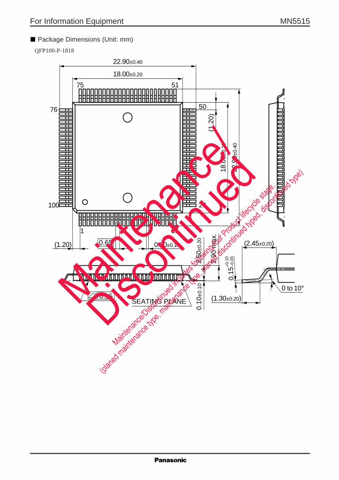
0.15
Package Dimensions (Unit: mm)
QFP100-P-1818
Mainten
ance/
Discon
tinued
Mainten
ance/D
iscont
inued
includ
es foll
owing
four P
roduct
lifecyc
le stag
e.
(planed
mainten
ance ty
pe, main
tenanc
e type,
planed
discon
tinued
typed,
discon
tinued
type)

Request for your special attention and precautions in using the technical information andsemiconductors described in this book
(1)If any of the products or technical information described in this book is to be exported or provided to non-residents, the laws and regulations of the exporting country, especially, those with regard to security export control, must be observed.
(2)The technical information described in this book is intended only to show the main characteristics and application circuit examples of the products, and no license is granted under any intellectual property right or other right owned by our company or any other company. Therefore, no responsibility is assumed by our company as to the infringement upon any such right owned by any other company which may arise as a result of the use of technical information described in this book.
(3)The products described in this book are intended to be used for standard applications or general electronic equipment (such as office equipment, communications equipment, measuring instruments and household appliances). Consult our sales staff in advance for information on the following applications: Special applications (such as for airplanes, aerospace, automobiles, traffic control equipment, combustion equipment, life support
systems and safety devices) in which exceptional quality and reliability are required, or if the failure or malfunction of the prod-ucts may directly jeopardize life or harm the human body. Any applications other than the standard applications intended.
(4)The products and product specifications described in this book are subject to change without notice for modification and/or im-provement. At the final stage of your design, purchasing, or use of the products, therefore, ask for the most up-to-date Product Standards in advance to make sure that the latest specifications satisfy your requirements.
(5)When designing your equipment, comply with the range of absolute maximum rating and the guaranteed operating conditions (operating power supply voltage and operating environment etc.). Especially, please be careful not to exceed the range of absolute maximum rating on the transient state, such as power-on, power-off and mode-switching. Otherwise, we will not be liable for any defect which may arise later in your equipment.
Even when the products are used within the guaranteed values, take into the consideration of incidence of break down and failure mode, possible to occur to semiconductor products. Measures on the systems such as redundant design, arresting the spread of fire or preventing glitch are recommended in order to prevent physical injury, fire, social damages, for example, by using the products.
(6)Comply with the instructions for use in order to prevent breakdown and characteristics change due to external factors (ESD, EOS, thermal stress and mechanical stress) at the time of handling, mounting or at customer's process. When using products for which damp-proof packing is required, satisfy the conditions, such as shelf life and the elapsed time since first opening the packages.
(7)This book may be not reprinted or reproduced whether wholly or partially, without the prior written permission of Matsushita Electric Industrial Co., Ltd.
Mainten
ance/
Discon
tinued
Mainten
ance/D
iscont
inued
includ
es foll
owing
four P
roduct
lifecyc
le stag
e.
(planed
mainten
ance ty
pe, main
tenanc
e type,
planed
discon
tinued
typed,
discon
tinued
type)