formula for electronics
DESCRIPTION
electronicsTRANSCRIPT
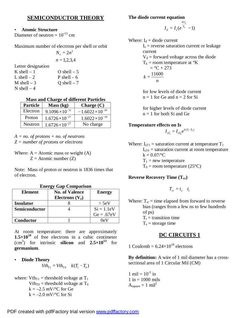
SEMICONDUCTOR THEORY • Atomic Structure Diameter of neutron = 10-13 cm Maximum number of electrons per shell or orbit
4,3,2,12 2
==
nnNe
Letter designation K shell – 1 O shell – 5 L shell – 2 P shell – 6 M shell – 3 Q shell – 7 N shell – 4
Mass and Charge of different Particles Particle Mass (kg) Charge (C) Electron 31101096.9 −× 19106022.1 −×− Proton 27106726.1 −× 19106022.1 −×+
Neutron 27106726.1 −× No charge A = no. of protons + no. of neutrons Z = number of protons or electrons Where: A = Atomic mass or weight (A)
Z = Atomic number (Z) Note: Mass of proton or neutron is 1836 times that of electron.
Energy Gap Comparison Element No. of Valence
Electrons (Ve)
Energy
Insulator 8 > 5eV Semiconductor 4 Si = 1.1eV
Ge = .67eV Conductor 1 0eV At room temperature: there are approximately 1.5×10¹⁰ of free electrons in a cubic centimeter (cm3) for intrinsic silicon and 2.5×10¹³ for germanium. • Diode Theory
)( 0101 TTkVthVth TT −+= where: VthT1 = threshold voltage at T1
VthT0 = threshold voltage at T0 k = –2.5 mV/°C for Ge k = –2.0 mV/°C for Si
The diode current equation
)1( −= k
d
TkV
sd eII Where: Id = diode current
Is = reverse saturation current or leakage current Vd = forward voltage across the diode Tk = room temperature at °K = °C + 273
nk 11600
=
for low levels of diode current n = 1 for Ge and n = 2 for Si for higher levels of diode current n = 1 for both Si and Ge
Temperature effects on Is
)( 01
01
TTksTsT eII −=
Where: IsT1 = saturation current at temperature T1 IsT0 = saturation current at room temperature
k = 0.07/°C T1 = new temperature
T0 = room temperature (25°C) Reverse Recovery Time (Trr)
tsrr ttT += Where: Trr = time elapsed from forward to reverse
bias (ranges from a few ns to few hundreds of ps)
Tt = transition time Ts = storage time
DC CIRCUITS 1 1 Coulomb = 6.24×10¹⁸ electrons By definition: A wire of 1 mil diameter has a cross-sectional area of 1 Circular Mil (CM) 1 mil = 10-3 in 1 in = 1000 mils Asquare = 1 mil2
PDF created with pdfFactory trial version www.pdffactory.com

22
4milDAcircle
π=
CMmilπ41 2 =
Type/Flavors of Quarks
Quark Symbol Charge Baryon no. Up U +2/3 1/3 Down D –1/3 1/3 Charm C +2/3 1/3 Strange S –1/3 1/3 Top T +2/3 1/3 Bottom B –1/3 1/3
Proton – 2 Up and 1 Down Neutron – 1 Up and 2 Down
Types of Battery Type Height (in) Diameter (in)
D 412 4
11 C 4
31 1 AA 8
71 169
AAA 431 8
3
tQI =
)(sec)();(
sondCCoulombAAmpere
QWV =
)()();(CCoulomb
JJouleVVolt
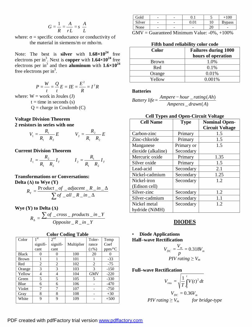
LRA
=ρ ftCMcmm −Ω
−Ω−Ω ;;
Resistivities of common metals and alloys
Material ρ (10-8Ω-m) Aluminum (Al) 2.6 Brass 6 Carbon 350 Constantan (60% Cu and 40% Ni) 50 Copper (Cu) 1.7 Manganin (84% Cu, 12%Mn & 4%Ni)
44
Nichrome 100 Silver (Ag) 1.5 Tungsten (W) 5.6
Absolute zero = 0 K = –273°C ρCu = 10.37 Ω–CM/ft
Temperature effects on resistance
1
2
1
2
tTtT
RR
++
= 1
11
tT +=α
)](1[ 12112 ttRR −+= α where: |T| = inferred absolute temperature, °C R2 = final resistance at final temp. t2 R1 = initial resistance at initial temp. t1 α1 = temp coefficient of resistance at t1 American Wire Gauge (AWG)
AWG #10: A = 5.261 mm2 AWG #12: A = 3.309 mm2 AWG #14: A = 2.081 mm2
Inferred Absolute Temp. for Several Metals
Material Inferred absolute zero, °C Aluminum -236 Copper, annealed -234.5 Copper, hard-drawn -242 Iron -180 Nickel -147 Silver -243 Steel, soft -218 Tin -218 Tungsten -202 Zinc -250
Temperature-Resistance Coefficients at 20 °C Material α20
Nickel 0.006 Iron, commercial 0.0055 Tungsten 0.0045 Copper, annealed 0.00393 Aluminum 0.0039 Lead 0.0039 Copper, hard-drawn 0.00382 Silver 0.0038 Zinc 0.0037 Gold, pure 0.0034 Platinum 0.003 Bras 0.002 Nichrome 0.00044 German Silver 0.0004 Nichrome II 0.00016 Manganin 0.00003 Advance 0.000018 Constantan 0.000008
PDF created with pdfFactory trial version www.pdffactory.com
LA
LA
RG σ
ρ===
1
where: σ = specific conductance or conductivity of the material in siemens/m or mho/m.
Note: The best is silver with 1.68×1024 free electrons per in3. Next is copper with 1.64×1024 free electrons per in3 and then aluminum with 1.6×1024 free electrons per in3.
RIR
EIEEtQ
tWP 2
2
=====
where: W = work in Joules (J) t = time in seconds (s) Q = charge in Coulomb (C) Voltage Division Theorem 2 resistors in series with one
ERR
RV21
11 +
= ERR
RV21
22 +
=
Current Division Theorem
TIRR
RI21
21 +
= TIRR
RI21
12 +
=
Transformations or Conversations: Delta (Δ) to Wye (Y)
∑ ∆∆
=____
_____PrinRallof
inRadjacentofoductRY
Wye (Y) to Delta (Δ)
YinROppositeYinproductscrossof
R___
____∑=∆
Color Coding Table
Color 1st signifi-cant
2nd signifi-cant
Multiplier
Toler-rance (±%)
Temp Coef ppm/°C
Black 0 0 100 20 0 Brown 1 1 101 1 -33 Red 2 2 102 2 -75 Orange 3 3 103 3 -150 Yellow 4 4 104 GMV -220 Green 5 5 105 5 -330 Blue 6 6 106 - -470 Violet 7 7 107 - -750 Gray 8 8 108 - +30 White 9 9 109 - +500
Gold - - 0.1 5 +100 Silver - - 0.01 10 Bypass None - - - 20 -
GMV = Guaranteed Minimum Value: -0%, +100%
Fifth band reliability color code Color Failures during 1000
hours of operation Brown 1.0%
Red 0.1% Orange 0.01% Yellow 0.001%
Batteries
Battery life)(_
)(_AdrawnAmperes
AhratinghourAmpere −=
Cell Types and Open-Circuit Voltage
Cell Name Type Nominal Open-Circuit Voltage
Carbon-zinc Primary 1.5 Zinc-chloride Primary 1.5 Manganese dioxide (alkaline)
Primary or Secondary
1.5
Mercuric oxide Primary 1.35 Silver oxide Primary 1.5 Lead-acid Secondary 2.1 Nickel-cadmium Secondary 1.25 Nickel-iron (Edison cell)
Secondary 1.2
Silver-zinc Secondary 1.2 Silver-cadmium Secondary 1.1 Nickel metal hydride (NiMH)
Secondary 1.2
DIODES
• Diode Applications Half–wave Rectification
mm
DC VVV 318.0==π
PIV rating ≥ Vm Full–wave Rectification
∫=t
rms dttVT
V0
2)(1
mDC VV 36.0= PIV rating ≥ Vm for bridge-type
PDF created with pdfFactory trial version www.pdffactory.com
PIV rating ≥ 2Vm for center-tapped • Other Semiconductor Devices Zener Diode
)( 01 TTVVT
Z
ZCC −
∆=
where: TCC = temperature coefficient T1–T0 = change in temperature VZ = Zener Voltage at T0 Basic Zener Regulator I. Vi and RL fixed (a) Determine the state of the Zener diode by
removing it from the network and calculating the voltage across the resulting open circuit.
(b) Substitute the appropriate equivalent circuit and solve for the desired unknown.
II. Fixed RL, variable Vi
L
ZSLi R
VRRV )(min
+= ZSRi VRIV += maxmax
III. Fixed Vi, variable RL
Zi
ZL VV
RVR−
=min min
maxL
ZL I
VR =
Varactor diode or Varicap diode
dT W
AC ε=
where: CT = transition capacitance which is due to the established covered charges on either side of the junction A = pn junction area Wd = depletion width
In terms of the applied reverse bias voltage:
nRT
T VVkC
)( +=
where: CT = transition capacitance which is due to the established covered charges on either side of the junction k = constant determined by the semiconductor material and construction technique VT = knee voltage VR = reverse voltage n = ½ for alloy junctions and ⅓ for diffused junctions
In terms of the applied reverse bias voltage:
n
T
R
T
VV
CC
+
=
1
)0(
where: C(0) = capacitance at zero-bias condition Also,
( )01 TTCCTC
OC −
∆=
where: TCC = temperature coefficient T1 – T0 = change in temperature C0 = capacitance at T0 Photodiode
JouleschhfW ;λ
==
where: W = energy associated with incident light waves
h = Planck’s constant (6.624×10⁻³⁴ J-sec) f = frequency 1eV = 1.6×10⁻⁹ J 1 Angstrom (Å) = 10-10 m Solar Cell
==
2
max
1)(cmWArea
PPP
i
Oη
where: η = efficiency P0 = electrical power output
Pi = power provided by the light source Pmax = maximum power rating of the device Area = in cubic centimeters Note: The power density received from the sun at sea level is about 1000 mW/cm2
BIPOLAR JUNCTION TRANSISTOR
150001.0150.0
===base
total
widthwidthRatio
• Basic Operation Relationship between IE, IB and IC:
CBE III +=
PDF created with pdfFactory trial version www.pdffactory.com

IC is composed of two components: oritymajorityC III min+=
DC Transistor Parameters
E
C
tconsVcbE
C
II
II
=
∆∆
==
α
αtan
B
C
tconsVceB
C
II
II
=
∆∆
==
β
βtan
where: IE = emitter current IB = base current IC = collector current α = CB short-circuit amplification factor
β = CE forward-current amplification factor Relationship between α and β:
1+=
ββ
α α
αβ
−=
1
Stability Factor (S):
CO
CCO I
IIS∆∆
=)( Unitless
BE
CCO V
IIS∆∆
=)( Siemens
β∆∆
= CCO
IIS )( Ampere
Small Signal Analysis A. Hybrid Model
02221
01211
VhIhIVhIhV
ino
ini
+=+=
If Vo = 0
in
i
IVh =11 ohms
If Iin = 0
012 V
Vh i= unitless
If Vo = 0
inIIh 0
21 = unitless
If Iin = 0
0
011 V
Ih = siemens
where: h11 = input-impedance, hi h12 = reverse transfer voltage ratio, hr
h21 = forward transfer current ratio, hf h22 = output conductance, ho
H-Parameters typical values
CE CB CC hi 1kΩ 20Ω 1kΩ hr 2.5×10⁻⁴ 3×10⁻⁴ ≈1 hf 50 -0.98 -50 ho 25μS 0.5μS 25μS
Comparison between 3 transistor configurations
CB CE CC Zi low moderate high Zo high moderate low Ai low high moderate Av high high low Ap moderate high low
shift none 180° none
B. Re Model Note: Common Base : hib = re ; hfb = –1 Common Emitter: β = hfe ; βre = hie
FIELD EFFECT TRANSISTORS • JFET
2
1
−=
P
GSDSSD V
VII P
DSSmo V
Ig 2=
0
12
=∆∆
=
−=
dsVgs
d
P
GS
P
DSSm V
IVV
VIg
50 ≤≤ GSV where: Id = drain current Idss = drain-source saturation current Vgs = gate source voltage Vp = Vgs (off), pinch-off voltage gm = gfs, device transconductance gmo = the maximum ac gain parameter of the JFET • MOSFET
2)( THGSDS VVkI −= 2/3.0 VmAk =
• FET biasing
PDF created with pdfFactory trial version www.pdffactory.com
DC bias of a FET requires setting the gate-source voltage, which results in a desired drain current. Vgg is used to reverse bias the gate so that Ig = 0.
POWER SUPPLY • Transformer
p
s
p
s
p
s
s
p
ZZ
NN
VV
II
a ====
where: a = turns ratio Vs = secondary induce voltage Vp = primary voltage Ns = no. of turns on the secondary windings Np = no. of turns on the primary windings Ip = current in the primary windings Is = current in the secondary windings
Zs = impedance of the load connected to the secondary winding Zp = impedance looking into the primary from source
• Rectifier Half–wave signal
mdc VV 318.0= 2m
rmsVV =
rmsdc VV 636.0= rmsVPIV 2= Ripple frequency = AC input frequency
Full–wave rectified signal (bridge type)
mdc VV 636.0= 2m
rmsV
V =
rmsdc VV 9.0= rmsVPIV 2= Ripple frequency = 2×AC input frequency
Full–wave with center-tapped transformer Vdc = 0.9Vrms of the half the secondary = 0.45Vrms of the full secondary = 0.637Vpk of half of the secondary = 0.637Vpk of the full secondary PIV = 1.414Vrms of full secondary
dc
r
VrmsV
DCACr )(
==
22)( dcrmsr VVrmsV −= where: r = ripple factor
Vr(rms) = rms value of the ripple voltage
Vdc = average value of the filter’s output voltage
mr VrmsV 385.0)( = half–wave rectified signal
mr VrmsV 308.0)( = full–wave rectified signal • Filter
32)(
3)(
)(ppVpVrmsV rr
r−
==
CRV
CI
fCIrmsV
L
dcdcdcr
4.24.234
)( ===
CI
VfC
IVppVVV dc
mdc
mr
mdc17.4
42)(
−=−=−
−=
%1004.2%1004.2
%100)(×=×=×=
CRCVI
VrmsVr
Ldc
dc
dc
r
where: Idc = the load current in mA C = filter capacitor in μF RL = load resistance at the filter stage in kΩ
Vm = the peak rectified voltage Idc = the load current in mA C = filter capacitor in μF f = frequency at 60 Hz • Regulator Voltage Regulation
%100.. ×−
=fload
floadnoload
VVV
RV
Stability factor (S)
in
out
VVS
∆∆
= (constant output current)
Improved series regulation
)( 22
21BEZo VV
RRRV +
+=
INSTRUMENTATION
• DC Ammeter Relationship between current without the ammeter and current with the ammeter
mo
o
wom
wm
RRR
II
+=
where: Iwm = current with meter Iwom = current without meter Ro = equivalent resistance
PDF created with pdfFactory trial version www.pdffactory.com
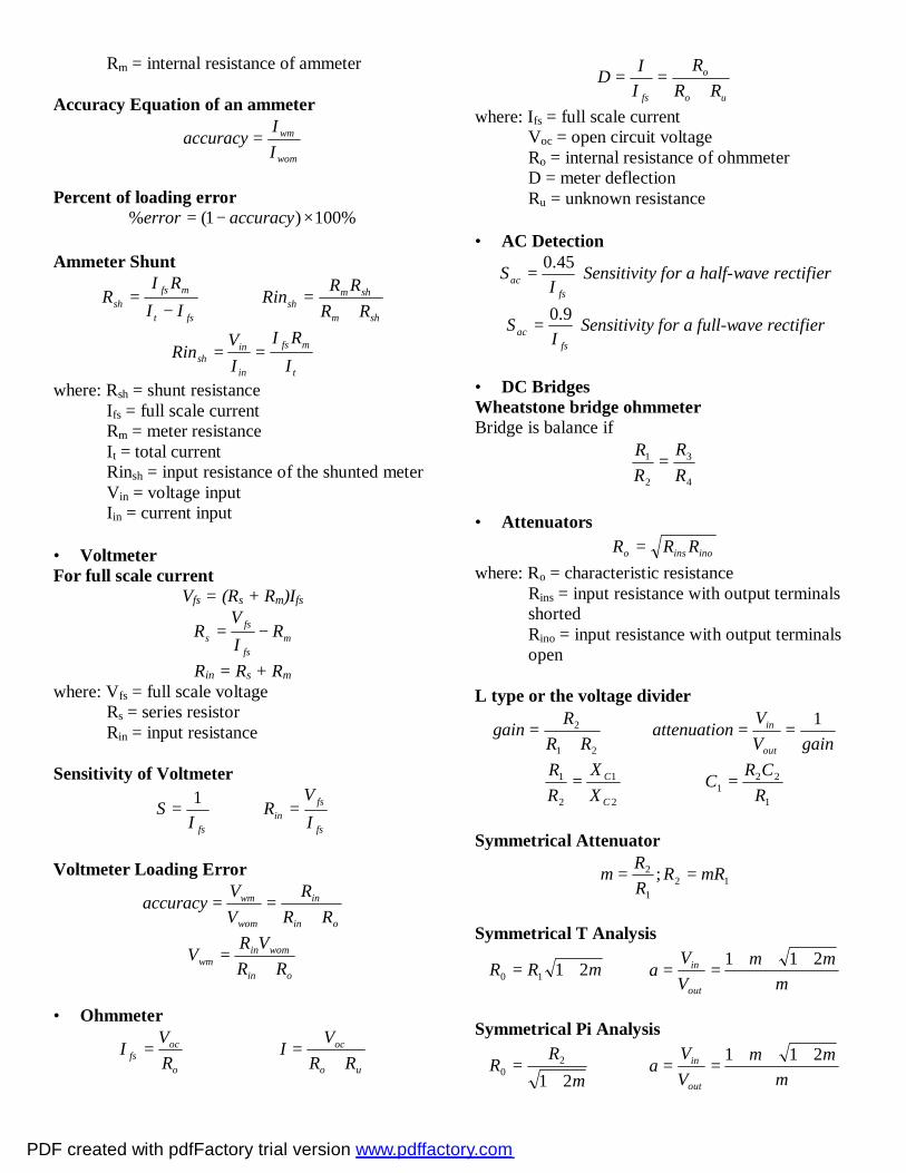
Rm = internal resistance of ammeter Accuracy Equation of an ammeter
wom
wm
IIaccuracy =
Percent of loading error
%100)1(% ×−= accuracyerror Ammeter Shunt
fst
mfssh II
RIR
−=
shm
shmsh RR
RRRin+
=
t
mfs
in
insh I
RIIV
Rin ==
where: Rsh = shunt resistance Ifs = full scale current Rm = meter resistance It = total current Rinsh = input resistance of the shunted meter Vin = voltage input Iin = current input • Voltmeter For full scale current
Vfs = (Rs + Rm)Ifs
mfs
fss R
IV
R −=
Rin = Rs + Rm where: Vfs = full scale voltage Rs = series resistor Rin = input resistance Sensitivity of Voltmeter
fsIS 1
= fs
fsin I
VR =
Voltmeter Loading Error
oin
in
wom
wm
RRR
VVaccuracy
+==
oin
wominwm RR
VRV+
=
• Ohmmeter
o
ocfs R
VI = uo
oc
RRVI+
=
uo
o
fs RRR
IID
+==
where: Ifs = full scale current Voc = open circuit voltage Ro = internal resistance of ohmmeter
D = meter deflection Ru = unknown resistance • AC Detection
fsac I
S 45.0= Sensitivity for a half-wave rectifier
fsac I
S 9.0= Sensitivity for a full-wave rectifier
• DC Bridges Wheatstone bridge ohmmeter Bridge is balance if
4
3
2
1
RR
RR
=
• Attenuators
inoinso RRR = where: Ro = characteristic resistance
Rins = input resistance with output terminals shorted Rino = input resistance with output terminals open
L type or the voltage divider
21
2
RRRgain+
= gainV
Vnattenuatioout
in 1==
2
1
2
1
C
C
XX
RR
= 1
221 R
CRC =
Symmetrical Attenuator
121
2 ; mRRRRm ==
Symmetrical T Analysis
mRR 2110 += m
mmVV
aout
in 211 +++==
Symmetrical Pi Analysis
mRR
212
0+
= m
mmVV
aout
in 211 +++==
PDF created with pdfFactory trial version www.pdffactory.com
Design Formulas for T Attenuator
oRa
aR2
12
1−
= oRaaR
11
2 −+
=
Design Formulas for T Attenuator
oRaaR
11
1 +−
= oRa
aR1
222 −
=
Variable Attenuator Analysis
R1 = R0 12
1 +=RRa
Design
R1 = R0 1
02 −
=aRR
03
1R
aR −=
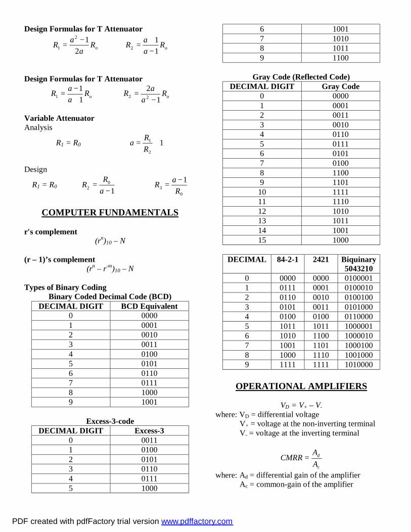
COMPUTER FUNDAMENTALS
r's complement
(rn)10 – N (r – 1)’s complement
(rn – r-m)10 – N Types of Binary Coding
Binary Coded Decimal Code (BCD) DECIMAL DIGIT BCD Equivalent
0 0000 1 0001 2 0010 3 0011 4 0100 5 0101 6 0110 7 0111 8 1000 9 1001
Excess-3-code
DECIMAL DIGIT Excess-3 0 0011 1 0100 2 0101 3 0110 4 0111 5 1000
6 1001 7 1010 8 1011 9 1100
Gray Code (Reflected Code)
DECIMAL DIGIT Gray Code 0 0000 1 0001 2 0011 3 0010 4 0110 5 0111 6 0101 7 0100 8 1100 9 1101 10 1111 11 1110 12 1010 13 1011 14 1001 15 1000
DECIMAL 84-2-1 2421 Biquinary
5043210 0 0000 0000 0100001 1 0111 0001 0100010 2 0110 0010 0100100 3 0101 0011 0101000 4 0100 0100 0110000 5 1011 1011 1000001 6 1010 1100 1000010 7 1001 1101 1000100 8 1000 1110 1001000 9 1111 1111 1010000
OPERATIONAL AMPLIFIERS
VD = V+ – V-
where: VD = differential voltage V+ = voltage at the non-inverting terminal V- = voltage at the inverting terminal
c
d
AACMRR =
where: Ad = differential gain of the amplifier Ac = common-gain of the amplifier
PDF created with pdfFactory trial version www.pdffactory.com

Slew rate
pko Vf
tVSR max2π=
∆∆
=
where: fmax = highest undistorted frequency Vpk = peak value of output sine wave Differentiator
dtdVRCV in
o −=
Integrator
dtVRC
V ino ∫−=1
Basic non-inverting amplifier
1
21RRgain +=
Basic inverting amplifier
1
2
RRgain −=
LOGIC GATES
• Boolean Algebra Postulated and Theorems of Boolean algebra
11
1'0
=+=+=+
=+
XXXX
XXXX
00
0'1
=•=•=•
=•
XXXX
XXXX
(Commutative Law)
XYYX +=+ XYYX •=• (Associative Law)
ZYXZYX ++=++ )()( ZXYYZX •=• )()( (Distributive Law)
YZXYZYX +=+ )( ))(()( ZYYXYZX ++=+
(Law of Absorption)
XXYXZX =++ )( XYXX =++ )( (De Morgan’s Theorem)
'')'( YXYX =+ '')'( YXXY +=
• Logic Family Criterion Propagation delay is the average transition delay time for a signal to propagate from input to output.
2PLHPHL
pttt +
=
where: tp = propagation delay tPHL = propagation delay high to low
transition tPLH = propagation delay low to high transition
Power dissipation is the amount of power that an IC drains from its power supply.
2)( CCLCCH
CCIIAVGI +
=
CCCCD VAVGIAVGP ×= )()( where: ICCH = current drawn from the power supply
at high level ICCL = current drawn from the power supply
at low level Noise Margin is the maximum noise voltage added to the input signal of a digital circuit that does not cause an undesirable change in the circuit output. Low State Noise Margin
OLILL VVNM −= where: NM = Noise Margin VIL = low state input voltage VOL = low state output voltage High State Margin
IHOHH VVNM −= where: NM = Noise Margin VIH = high state input voltage VOH = high state output voltage Logic Swing
OLOHls VVV −= where: Vls = voltage logic swing VOH = high state output voltage VOL = low state output voltage Transition Width
ILIHtw VVV −= where: Vtw = voltage transition width VIH = high state input voltage VIL = low state input voltage
PDF created with pdfFactory trial version www.pdffactory.com
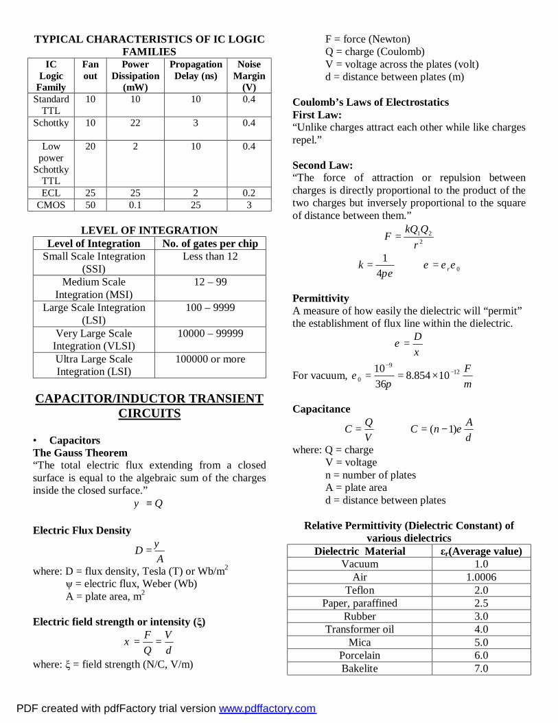
TYPICAL CHARACTERISTICS OF IC LOGIC FAMILIES
IC Logic
Family
Fan out
Power Dissipation
(mW)
Propagation Delay (ns)
Noise Margin
(V) Standard
TTL 10 10 10 0.4
Schottky
10 22 3 0.4
Low power
Schottky TTL
20 2 10 0.4
ECL 25 25 2 0.2 CMOS 50 0.1 25 3
LEVEL OF INTEGRATION
Level of Integration No. of gates per chip Small Scale Integration
(SSI) Less than 12
Medium Scale Integration (MSI)
12 – 99
Large Scale Integration (LSI)
100 – 9999
Very Large Scale Integration (VLSI)
10000 – 99999
Ultra Large Scale Integration (LSI)
100000 or more
CAPACITOR/INDUCTOR TRANSIENT
CIRCUITS • Capacitors The Gauss Theorem “The total electric flux extending from a closed surface is equal to the algebraic sum of the charges inside the closed surface.”
Q≡ψ Electric Flux Density
AD ψ
=
where: D = flux density, Tesla (T) or Wb/m2 ψ = electric flux, Weber (Wb) A = plate area, m2 Electric field strength or intensity (ξ)
dV
QF
==ξ
where: ξ = field strength (N/C, V/m)
F = force (Newton) Q = charge (Coulomb) V = voltage across the plates (volt) d = distance between plates (m) Coulomb’s Laws of Electrostatics First Law: “Unlike charges attract each other while like charges repel.” Second Law: “The force of attraction or repulsion between charges is directly proportional to the product of the two charges but inversely proportional to the square of distance between them.”
221
rQkQF =
πε41
=k 0εεε r=
Permittivity A measure of how easily the dielectric will “permit” the establishment of flux line within the dielectric.
ξε
D=
For vacuum, mF12
9
0 10854.83610 −
−
×==π
ε
Capacitance
VQC =
dAnC ε)1( −=
where: Q = charge V = voltage n = number of plates A = plate area d = distance between plates
Relative Permittivity (Dielectric Constant) of
various dielectrics Dielectric Material εr(Average value)
Vacuum 1.0 Air 1.0006
Teflon 2.0 Paper, paraffined 2.5
Rubber 3.0 Transformer oil 4.0
Mica 5.0 Porcelain 6.0 Bakelite 7.0
PDF created with pdfFactory trial version www.pdffactory.com
Glass 7.5 Distilled water 80.0
Barium-strontium titanite (ceramic)
7500.0
Dielectric strength of some dielectric materials
Dielectric Material
Dielectric Strength (Average Value) in V/mil
Air 75 Barium-strontium titanite (ceramic)
75
Porcelain 200 Transformer oil 400
Bakelite 400 Rubber 700
Paper, paraffined 1300 Teflon 1500 Glass 3000 Mica 5000
Energy stored
CQCVE22
1 22 ==
Capacitors in Series
n
T
CCCC
C1...111
1
321
++++=
nT QQQQQ ===== ...321 Capacitors in Parallel
nT CCCCC ++++= ...321
nT QQQQQ ++++= ...321 Other capacitor configurations Composite medium parallel-plate capacitor
++
=
3
3
2
2
1
1
0
rrr
dddAC
εεε
ε
where: d1, d2 and d3 = thickness of dielectrics with relative permittivities of εr1, εr2 and εr3 respectively Medium partly air parallel-plate capacitor
−−
=
r
ttd
AC
ε
ε 0
Cylindrical capacitor 910
log4.41
−×
=
ab
C rlε
where: a = diameter of single core cable conductor and surrounded by an insulation of inner diameter b
εr = relative permittivity of the insulation of the cable
l = length of the cylindrical capacitor Capacitance of an isolated sphere
C = 4πεr where: r = radius of the isolated sphere in a medium
of relative permittivity εr Capacitance of concentric spheres a.) When outer sphere earthed
)(4
ababC−
= πε
Where: a and b are radii of two concentric spheres ε = permittivity of the dielectric between two spheres
b.) When inner sphere is earthed
)(4
2
abbC−
= πε
• Inductors Inductance (L) is a measure of the ability of a coil to oppose any change in current through the coil and to store energy in the form of a magnetic field in the region surrounding the coil. In terms of physical dimensions,
l
ANL2
µ= Henry
where: μ = permeability of the core (H/m) N = number of turns A = area of the core (m2) l = mean length of the core (m) In terms of electrical definition,
didNL φ
=
PDF created with pdfFactory trial version www.pdffactory.com

Faraday’s Law “The voltage induced across a coil of wire equals the number of turns in the coil times the rate of change of the magnetic flux.”
dtdNeinφ
=
where: N = number of turns of the coil
dtdφ = change in the magnetic flux
Lenz’s Law “An induced effect is always such as to oppose the cause that produced it.”
dtdNeinφ
−=
Induced voltage by Faraday’s Law
dtdiLeL =
Energy stored
2
21 LIWL =
Inductance without mutual inductance in series
nT LLLLL ++++= ...321 With mutual inductance (M) a.) when fields are aiding
MLLLTa 221 ++= b.) when fields are opposing
MLLLTo 221 −+= Total inductance without mutual inductance (M)
n
T
LLLL
L1...111
1
321
++++=
With mutual inductance (M) a.) when fields are aiding
MLLMLLL aT 221
221
)( −+−
=
b.) when fields are opposing
MLLMLLL oT 221
221
)( ++−
=
Mutual inductance It is a measure of the amount of inductive coupling that exists between the two coils.
21LLkM =
4ToTa LLM −
=
where: k = coupling coefficient L1 and L2 = self-inductances of coils 1 and 2 LTa and LTo = total inductances with mutual
inductance Coupling coefficient (k)
21LLMk =
1
21
________
LbyproducedfluxLandLbetweenlinkagefluxk =
Formulas for other coil geometries (a) LONG COIL
l
ANL2
µ=
(b) SHORT COIL
dANL45.0
2
+=
lµ
where: L = inductance (H) μ = permeability (4π×10-7 for air)
N = number of turns A = cross-sectional area of the coil (m2) l = length of the core (m) d = diameter of core (m) (c) TOROIDAL COIL with rectangular cross-
section
1
22
ln2 d
dhNLπ
µ=
where: h = thickness d1 and d2 = inner and outer diameters (d) CIRCULAR AIR-CORE COIL
bRRNL
1096)(07.0 2
++=
l
22bdR +=
where: L = inductance (μH) N = number of turns d = core diameter, in
PDF created with pdfFactory trial version www.pdffactory.com
b = coil build-up, in l = length, in (e) RECTANGULAR AIR-CORE COIL
bCCNL
109908.1)(07.0 2
++=
l
where: L = inductance (μH) C = d + y + 2b d = core height, in y = core width, in b = coil build-up, in l = length, in (f) MAGNETIC CORE COIL (no air gap)
c
ANLl
µ2012.0=
(g) MAGNETIC CORE COIL (with air gap)
µc
g
ANLl
l +=
2012.0
where: L = inductance (μH) N = number of turns A = effective cross-sectional area, cm2 cl = magnetic path length, cm gl = gap length, cm Μ = magnetic permeability
• DC Transient Circuits
Circuit Element
Voltage across
Current flowing
R iRv = Rvi =
L dtdiLv = vdt
Li ∫=
1
C idt
CCqv ∫==
1 dtdvCi =
Response of L and C to a voltage source Circuit Element @ t = 0 @ t = ∞
L open short C short open
RL Transient Circuit Storage Cycle:
−=
−=
−−τt
tLR
eREe
REi 11
RL
=τ
−=
− tLR
R eEv 1 t
LR
L Eev−
=
Decay Phase:
τt
tLR
eREe
REi
−−==
TRL
=τ RRRT += 1
RC Transient Circuit Charging Cycle:
( ) RCt
eECqECq−
−+= 0
−=
−RCt
eECq 1 with q0 = 0
RCt
eREi
−= RC
t
R Eev−
=
−=
−RCt
C eEv 1 RC=τ
Discharging Phase:
RCt
C Eev−
= RC=τ RLC Transient Circuits Conditions for series RLC transient circuit: (1) @ t = 0, i = 0 (2) @ t = 0, Ldi/dt = E Current equations Case 1 – Overdamped case
when LCL
R 12
2
>
then
trtr eCeCi 2121 +=
21 CC −= L
ECβ22 −=
βα +=1r βα −=2r
LR
2−=α
LCLR 1
2−
=β
Case 2 – Critically damped case
when LCL
R 12
2
=
then
)( 21 tCCei t += α
PDF created with pdfFactory trial version www.pdffactory.com

01 =C LEC =2
LR
2−=α
Case 2 – Underdamped case
when LCL
R 12
2
<
then
)sincos( 21 tCCei t βα +=
LR
2−=α
LCLR 1
2−
=β
01 =C L
ECβ
=2
AC CIRCUITS 1
• Introduction to AC: Formulas
Form factor 11.1637.0707.0
===m
m
avg
rms
VV
VV
Peak factor 4142.1707.0
===m
m
rms
m
VV
VV
fLX L π2= fC
X C π21
=
• Series AC circuits Series RL Circuit Total voltage, VT
θ∠=+= TLRT VjVVV
22LRT VVV +=
R
L
VV1tan −=θ
Total impedance, Z
θ∠=+= ZjXRZ L
22LXRZ +=
RX L1tan−=θ
Series RC Circuit Total voltage, VT
θ∠=−= TCRT VjVVV
22CRT VVV +=
R
C
VV1tan −=θ
Total impedance, Z θ∠=−= ZjXRZ C
22CXRZ +=
RX C1tan −−=θ
Series RLC Circuit Total voltage, VT
θ∠=−+= TCLRT VjVjVVV
22 )( CLRT VVVV −+= R
CL
VVV )(
tan 1 −±= −θ
Total impedance, Z
θ∠=−+= ZjXjXRZ CL 22 )( CL XXRZ −+=
RXX CL )(
tan 1 −±= −θ
Total Current, IT
ZVI T
T =
• Parallel AC circuits Parallel RL Circuit Total Current, IT
θ∠=−= TLRT IjIII
22LRT III +=
R
L
II1tan −−=θ
Total admittance, Y
θ∠=−= YjBGY L
22LBGY +=
GBL1tan −−=θ
Parallel RC Circuit Total Current, IT
θ∠=+= TCRT IjIII
22CRT III +=
R
C
II1tan −=θ
Total Admittance, Y
θ∠=+= YjBGY C
22CBGY +=
GBC1tan −=θ
PDF created with pdfFactory trial version www.pdffactory.com
Parallel RLC Circuit Total Current, IT
θ∠=−+= TLCRT IjIjIII 22 )( LCRT IIII −+=
R
LC
III )(
tan 1 −±= −θ
Total admittance, Y
θ∠=−+= YjBjBGY LC 22 )( LC BBGY −+=
GBB LC )(
tan 1 −±= −θ
Total impedance, Z Total voltage, VT
YZ 1
= ZIV TT =
Power of AC Circuits True/Real/Average/Active Power
θcos2
2TTRR
RR IVVI
RVRIP ====
Reactive Power
θsin2
2TTXX
eq
xeqX IVVI
XV
XIQ ====
Apparent Power
TTT
T IVZ
VZIQ ===2
2
==SP
θcos Power Factor (PF)
==SQ
θsin Reactive Factor (RF)
θ∠=±= SjQPS 22 QPS +=
PQ1tan −±=θ
• Values of other alternating waveforms Symmetrical Trapezoid
prms Vb
abaV )(577.0 −+= pavg V
bbaV
2+
=
DC Pulse
baVV prms =
baVV pavg =
Triangular or Sawtooth
prms VV 577.0= pavg VV 5.0= Sine wave on dc level
2
22 p
DCrms
VVV +=
Square wave
prms VV = pavg VV = White Noise
prms VV41
≈
ENERGY CONVERSION
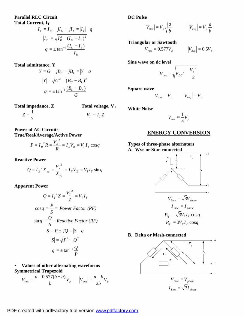
Types of three-phase alternators A. Wye or Star-connected
phaseLine VV 3=
phaseLine II =
θφ cos33 LL IVP = θφ cos33 PP IVP =
B. Delta or Mesh-connected
phaseLine VV =
phaseLine II 3=
PDF created with pdfFactory trial version www.pdffactory.com

θφ cos33 LL IVP = θφ cos33 PP IVP =
Frequency of the AC Voltage Generated in an Alternator
120PNf =
where: f = frequency (Hz) P = number of poles (even number) N = speed of prime mover (rpm) Speed Characteristics of DC Motors
φc
sE
kH =
where: Ec = counter emf ks = speed constant φ = flux Torque Characteristics of DC Motors
at IkT φ= where: Ia = armature current kt = torque constant φ = flux Speed of an AC Motor
PfN 120
=
where: N = synchronous speed (rpm) f = frequency (Hz)
P = number of poles
OSCILLATORS • Introduction Oscillator Requirements a. Amplifier b. Tank circuit c. Feedback Overall gain with feedback
AAA f β+
=1
Barkhausen Criterion for Oscillation a. The net gain around the feedback loop must be
no less than one; and b. The net phase-shift around the loop must be a
positive integer multiple of 2π radians or 360°.
Mathematically, 1≥Aβ
°×= 360nφ ...3,2,1=n
Basic Configuration of a Resonant Circuit Oscillator
• LC Oscillators Resonant-Frequency Feedback Oscillators
Oscillator Type X1 X2 X3 Hartley L L C Colpitts C C L Clapp C C Series LC (net L)
Pierce Crystal C C Crystal (net L) A. Hartley Oscillator Amplifier gain without feedback,
eV r
RA −=
for a common-emitter configuration The feedback factor,
1
2
LL
−=β
To maintain the oscillation,
2
1
LL
rRAe
V ==
The frequency of oscillation is
CLf
eqπ21
0 =
where MLLLeq 221 ++=
21LLM =
PDF created with pdfFactory trial version www.pdffactory.com

B. Colpitts Oscillator Amplifier gain without feedback,
eV r
RA −=
The feedback factor,
2
1
CC
−=β
The frequency of oscillation is
eqLCf
π21
0 =
where
21
21
CCCCCeq +
=
To maintain the oscillation,
1
2
CC
rRAe
V ==
C. Clapp Oscillator The frequency of oscillation is
eqLCf
π21
0 =
where
321
1111
CCC
Ceq
++=
• Crystal Oscillators Frequency drift LC: 0.8% Crystal: 0.0001% (1 ppm) Natural frequency of vibration
fthickness 1
α
The thicker the crystal, the lower its frequency of vibration Series and Parallel Resonant Frequencies Series
srs LC
fπ2
1=
Parallel
ms
msrp
CCCC
Lf
+
=
π2
1
Note: Series resonant frequency, frs is slightly lower than parallel resonant frequency, frp. • RC Oscillators RC Phase-Shift Oscillator The gain of the basic inverting amplifier is,
s
fV R
RA −=
The feedback factor is,
291
−=β
To maintain the oscillation,
29−=−=s
fV R
RA
The frequency of oscillation is,
621
0 RCf
π=
Wien Bridge Oscillator The open-loop gain is
31 =+=s
fV R
RA
The feedback factor is
31
=β
To maintain the oscillation,
2=s
f
RR
The frequency of oscillation is,
22110 2
1CRCR
fπ
=
Neglecting loading effects of the op-amp input and output impedances, the analysis of the bridge results in
PDF created with pdfFactory trial version www.pdffactory.com

1
2
2
1
CC
RR
RR
s
f += (bridge-balance condition)
Therefore, for the bridge to be balanced,
R1 = R2 = R and C1 = C2 = C The frequency of oscillation
RCf
π21
0 =
FEEDBACK AMPLIFIERS
• Types of Feedback Connections Equations of open-loop gain, feedback factor and closed-loop gain for different types of feedback
Feedback Connection
Source Signal
Output Signal
A β Af
Voltage Series
Voltage Voltage
i
o
vv
o
f
vv
s
o
vv
Current Series
Voltage Current
i
o
vi
o
f
iv
s
o
vi
Voltage Shunt
Current Voltage
i
o
iv
o
f
vi
s
o
iv
Current Shunt
Current Current
i
o
ii
o
f
ii
s
o
ii
Note: Some references try to designate the following terms to describe the four main types of feedback equations.
2. Series-shunt = Voltage series 3. Series-series = Current series 4. Shunt-shunt = Voltage shunt 5. Shunt-series = Current-shunt
• Negative Feedback Equations
AAA f β+
=1
where: A = gain without feedback (open-loop gain) Af = gain with feedback (closed-loop gain) 1 + βA = desensitivity or sacrifice factor βA = loop gain
Equations of closed-loop gain for different types of feedback connections
Feedback Type
Gain with Feedback
Type of Amplifier
Voltage Series
v
vvf A
AAβ+
=1
Voltage
Amplifier
Current Series
m
mmf G
GGβ+
=1
Transconductance
Amplifier
Voltage Shunt
m
mmf R
RRβ+
=1
Transresistance
Amplifier
Current Shunt
i
iif A
AAβ+
=1
Currrent
Amplifier
• Performance Characteristics of Negative
Feedback Networks Equations of amplifier impedance levels when
using negative feedback connection Feedback
Type Input
Resistance Output
Resistance Voltage Series
)1( ARi β+ increased A
Ro
β+1
decreased Current Series
)1( ARi β+ increased
)1( ARo β+ increased
Voltage Shunt A
Ri
β+1
decreased A
Ro
β+1
decreased Current Shunt A
Ri
β+1
decreased
)1( ARo β+ increased
AdA
AAdA
f
f
β+=
11
where: f
f
AdA
= change in gain with feedback
A
dA = change in gain without feedback
magnitude, |βA| = 1 phase-shift, θ = 180°
The limiting condition is for the negative feedback amplifiers.
PDF created with pdfFactory trial version www.pdffactory.com
AC CIRCUITS 2 • Series Resonance
LCf r
π21
=
where: fr = resonant frequency L = Inductance C = Capacitance Characteristics of series resonance 1. At resonance, XL = XC, VL = VC. 2. At resonance, Z is minimum. Z = R. 3. At resonance, I is maximum. I = E/R. 4. At resonance, Z is resistive. θ = 0° (I in phase
with E). 5. At f < fr, Z is capacitive. θ = + (I Leads E). 6. At f > fr, Z is inductive. θ = – (I Lags E). Quality Factor (Q) of a resonant circuit:
RofpowerActiveCorLeitherofpoweractiveQ
_________Re
=
CL
RRX
RXQ CL 1
===
Resonant Rise in Voltage
QEVV CL == Bandwidth (BW) is the range of frequencies over which the operation is satisfactory and is taken between two half-power (3dB down) points.
QfffBW r=−= 12
If Q ≥ 10; then fr bisects BW
21BWff r −=
22BWff r +=
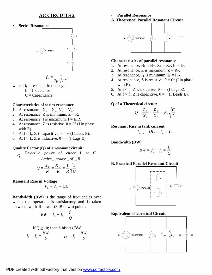
• Parallel Resonance A. Theoretical Parallel Resonant Circuit
Characteristics of parallel resonance 1. At resonance, BL = BC, XL = XC, IL = IC. 2. At resonance, Z is maximum. Z = RP. 3. At resonance, IT is minimum. IT = IRP. 4. At resonance, Z is resistive. θ = 0° (I in phase
with E). 5. At f < fr, Z is inductive. θ = – (I Lags E). 6. At f > fr, Z is capacitive. θ = + (I Leads E). Q of a Theoretical circuit:
LCR
XR
XRQ P
C
P
L
P ===
Resonant Rise in tank current
CLTk IIQII ===tan
Bandwidth (BW)
QfffBW r=−= 12
B. Practical Parallel Resonant Circuit
Equivalent Theoretical Circuit
PDF created with pdfFactory trial version www.pdffactory.com
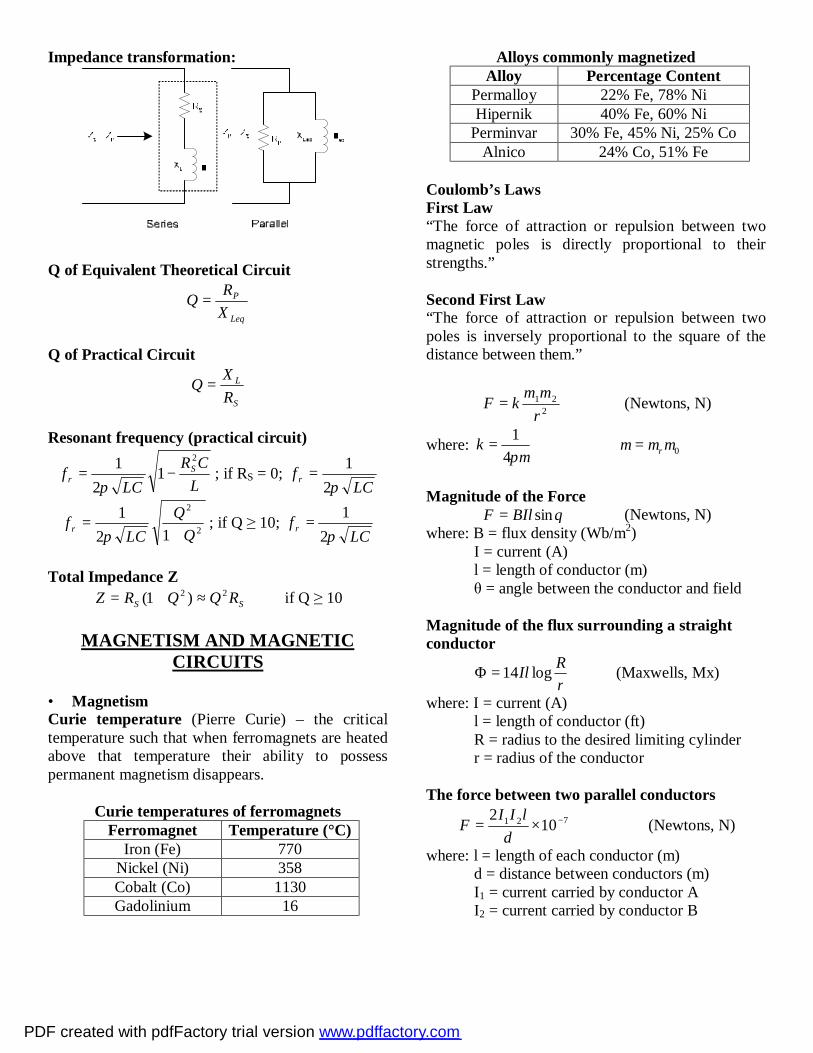
Impedance transformation:
Q of Equivalent Theoretical Circuit
Leq
P
XRQ =
Q of Practical Circuit
S
L
RXQ =
Resonant frequency (practical circuit)
LCR
LCf S
r
2
12
1−=
π; if RS = 0;
LCf r
π21
=
2
2
121
LCf r +
=π
; if Q ≥ 10; LC
f rπ2
1=
Total Impedance Z
SS RQQRZ 22 )1( ≈+= if Q ≥ 10
MAGNETISM AND MAGNETIC CIRCUITS
• Magnetism Curie temperature (Pierre Curie) – the critical temperature such that when ferromagnets are heated above that temperature their ability to possess permanent magnetism disappears.
Curie temperatures of ferromagnets Ferromagnet Temperature (°C)
Iron (Fe) 770 Nickel (Ni) 358 Cobalt (Co) 1130 Gadolinium 16
Alloys commonly magnetized Alloy Percentage Content
Permalloy 22% Fe, 78% Ni Hipernik 40% Fe, 60% Ni
Perminvar 30% Fe, 45% Ni, 25% Co Alnico 24% Co, 51% Fe
Coulomb’s Laws First Law “The force of attraction or repulsion between two magnetic poles is directly proportional to their strengths.” Second First Law “The force of attraction or repulsion between two poles is inversely proportional to the square of the distance between them.”
221
rmmkF = (Newtons, N)
where: πµ41
=k 0µµµ r=
Magnitude of the Force
θsinBIlF = (Newtons, N) where: B = flux density (Wb/m2) I = current (A) l = length of conductor (m) θ = angle between the conductor and field Magnitude of the flux surrounding a straight conductor
rRIl log14=Φ (Maxwells, Mx)
where: I = current (A) l = length of conductor (ft) R = radius to the desired limiting cylinder r = radius of the conductor The force between two parallel conductors
721 102 −×=
dlIIF (Newtons, N)
where: l = length of each conductor (m) d = distance between conductors (m) I1 = current carried by conductor A I2 = current carried by conductor B
PDF created with pdfFactory trial version www.pdffactory.com

Magnitude of the flux between two parallel conductors
r
rdIl )(log28 −=Φ (Maxwells, Mx)
where: I = current (A) l = length of conductor (ft)
r = radius of each conductor (m) d = distance of the conductors from center to center (m)
• Magnetic Circuits
AB Φ
=
where: B = Flux density in Tesla (T) Φ = Flux lines in Webers (Wb) A = Area in square meters (m2) Note: 1 Tesla = 1 Wb/m2 Permeability
mHor
meterAmpereWeber
−×= −7
0 104πµ
Note: μ = μ0; μr = 1 → non–magnetic μ < μ0; μr < 1 → diamagnetic μ > μ0; μr > 1 → paramagnetic μ >> μ0; μr >> 1 → ferromagnetic (μr ≥ 100)
AL
µ=ℜ
where: ℜ = reluctance L = the length of the magnetic path A = the cross-sectional area Note: The t in the unit A-t/Wb is the number of turns of the applied winding. Different units of Reluctance (ℜ )
a.) Weber
turnAmpere − b.) Maxwell
turnAmpere −
c.) MaxwellGilbert d.)
WeberGilbert
Note: 1 Weber = 1×10⁸ maxwells
1 Gilbert = 0.7958 ampere-turns 1 Gauss = 1 maxwell/cm2
Ohm’s Law for Magnetic Circuits
OppositionCauseEffect =
Then,
ℜℑ
=Φ
where: ℜ = reluctance ℑ = magnetomotive force, mmf (Gb or At) Φ = flux (Weber or Maxwells)
Comparison bet. Magnetic and Electric Circuits
Electric Circuits Magnetic Circuits Resistance, R (Ω) Reluctance, ℜ (Gb/Mx)
Current, I (A) Flux, Φ (Wb or Mx) emf, V (V) mmf, ℑ (Gb or At)
Total reluctance in series
nT ℜ++ℜ+ℜ=ℜ ...21 Total reluctance in parallel
nT ℜ++
ℜ+
ℜ=
ℜ1...111
21
Total flux in series
nT Φ==Φ=Φ=Φ ...21 Total flux in parallel
nT Φ++Φ+Φ=Φ ...21 Energy stored
2
21
Φℜ=mW Joules
Magnetomotive force (mmf, ℑ )
NI=ℑ Ampere – turns, At NIπ4.0=ℑ Gilberts, Gb
mmf of an air gap
0µdBmmf = Ampere-turns
Tractive force or lifting force of a magnet
=
0
2
21
µABF Newtons
PDF created with pdfFactory trial version www.pdffactory.com
Magnetizing Force (H)
l
ℑ=H
l
NIH =
Note: The unit of H is At/m Permeability – the ratio of flux density to the magnetizing force.
HB
=µ
B and H of an infinitely long straight wire
rIB
πµ2
= r
IHπ2
=
Steinmetz’s Formula of Hysteresis Loss
6.1mh fBW η= 3m
J
where: η = hysteresis coefficient f = frequency Bm = maximum flux density Ampere’s Circuital Law “The algebraic sum of the rises and drops of the mmf a closed loop of a magnetic circuit is equal to zero; that is, the sum of the mmf rises equals the sum of the mmf drops around a closed loop.”
0=∩ℑ∑ (for magnetic circuits) Source of mmf is expressed by the equation
NI=ℑ (At) For mmf drop,
ℜΦ=ℑ (At) A more practical equation of mmf drop
lH=ℑ (At)
PDF created with pdfFactory trial version www.pdffactory.com