fpga implementation of systolic array architecture … (part-4)/i021043950.pdffpga implementation of...
TRANSCRIPT

IOSR Journal of Engineering (IOSRJEN)
e-ISSN: 2250-3021, p-ISSN: 2278-8719, www.iosrjen.org
Volume 2, Issue 10 (October 2012), PP 39-50
www.iosrjen.org 39 | P a g e
FPGA Implementation of Systolic Array Architecture for 3D-
DWT Optimizing Speed and Power
Prof.C.Chandrasekhar1, Dr.S.Narayana Reddy
2
1( Porf. & HOD in Dept.of ECE,SVCET ,CHITTOOR ,)
2 (Prof. & HOD in Dept.of ECE, S.V.University collage of Engg. , Tirupathi
ABSTRACT: Demand for high speed and low power architectures for image/video compression algorithms
are increasing with scaling in VLSI technology. Video sequences are considered as 3D sequences and are
compressed using 3D DWT architectures. In this paper, systolic array architectures for 2D DWT have been
modified and have been used in computing 3D DWT and 3D IDWT. The architecture uses intermediate
memories efficiently in storing the intermediate coefficients and a memory control module controls the data path
operation. The systolic array is designed with a constant coefficient multiplier and a fast adder to realize the
accumulator. Daub-8 wavelet is used to compute DWT sub bands; the coefficients are scaled and stored in
memory for processing of input in all three dimensions. The design is 10% faster and occupies 44% less area
compared with reference design. The 3D DWT designed is 40% faster and consumes 45% less power compared
with reference design. The developed 2D and 3D DWT can be used as an IP for video and image processing
applications.
KEY WORDS - 3D-DWT, 3D-DWT Systolic Array Architecture, 3D-DWTSA FPGA implementation
I. INTRODUCTION In the last decade, there has been an enormous increase in the applications of wavelets in various
scientific disciplines to relate the discrete-time filter bank with the theory of continuous time function space.
Typical applications of wavelets include signal processing, image processing, numerical analysis, statistics,
biomedicine, etc. Wavelet
transform offers a wide variety of useful features, in contrast to other transforms, such as Fourier transform or
cosine transform. Some of these are as follows:
adaptive time-frequency windows;
lower aliasing distortion for signal processing applications;
computational complexity of O (N), where N is the number of data samples;
inherent scalability;
Efficient VLSI implementation.
Since discrete wavelet transform (DWT) requires intensive computations, several architectural
solutions using special purpose parallel processors have been proposed in order to meet the real time
requirement in many applications. The solutions include parallel filter architecture, SIMD linear array
architectures, SIMD multigrid architecture,2-D block based architecture, and the architectures, SIMD linear
array architecture and the SIMD multigrid architecture are special purpose parallel processors that implement
the high level abstraction of the pyramid algorithm. The two-dimensional (2-D) block –based architecture is
VLSI implementations that uses four multiply and accumulate (MAC) units to execute the forward and inverse
transforms. It requires a small on-chip memory and implements 2-D wavelet transform directly without data
transportation. However, this feature can be a drawback in certain applications. In addition, the block-based
architecture may introduce block boundary effects degrading the visual quality. The AWARE‟s WTP is capable
of computing forward and inverse wavelet transforms for one-dimensional (1-D) input data using a maximum of
six filter coefficients. It can be cascaded to execute transforms AWARE‟s wavelet transform processor. The first
three architectures, namely the parallel filter using higher order filters. The WTP has been clocked at speeds of
30 MHz and offers 16b precision on input and output data. The DWT computation is executed in a synchronous
pipeline fashion and is under complete user control. However, the AWARE‟s WTP is a complex design
requiring extensive user control. Programming such a device is therefore tedious, difficult, and time consuming.
The 3D wavelet decomposition is computed by applying three separate 1D transforms along the coordinate axes
of the video data. the 3D data is usually organized frame by frame. The single frames have again rows and
columns as in the 2D case, x and y direction often denoted as “spatial co-ordinates” where as for video data a
third dimension z for “time” is added. In the case of 2D decompositions, it does not matter in which order the

FPGA Implementation of Systolic Array Architecture for 3D-DWT Optimizing Speed and Power
www.iosrjen.org 40 | P a g e
filtering is performed. A 2-D filtering frame by frame with subsequent temporal filtering, three 1-D filtering
along y, t, and x axes, one decomposition step results in 8 frequency sub bands out of which only the
approximation data is processed further in the next decomposition step. The paper “Low-Power And High-
Speed VLSI Architecture For Lifting-Based Forward And Inverse Wavelet Transform”[1] proposed by
Xuguang Lan and Nanning Zheng, presents the low-power, high-speed architecture which performs two-
dimension forward and inverse discrete wavelet transform (DWT) for the set of filters in JPEG2000 using line
based and lifting scheme. Anirban Das, Anindya Hazra, and Swapna Banerjee have proposed the architecture of
the lifting based running 3-D discrete wavelet transform (DWT), which is a powerful image and video
compression algorithm in the paper “An Efficient Architecture for 3-D Discrete Wavelet Transform”[2]. The
proposed design is one of the first lifting based complete 3-DDWT architectures without group of pictures
restriction. Chin-Fa Hsieh , Tsung-Han Tsai, Neng-Jye Hsu, and Chih-Hung Lai, proposed[3] a novel, efficient
VLSI architecture for the implementation of one-dimension, lifting-based discrete wavelet transform (DWT).
Both folded and the pipelined schemes are applied in the proposed architecture the former scheme supports
higher hardware utilization and the latter scheme speed up the clock rate of the DWT. Jen-Shiun Chiang, and
Chih-Hsien Hsia have proposed a highly efficient VLSI architecture for 2-D lifting-based 5/3 filter discrete
wavelet transform (DWT) in “An Efficient VLSI Architecture for 2-D DWT using Lifting Scheme”[4] paper.
The architecture is based on the pipelined and folding scheme processing to achieve near 100% hardware
utilization ratio and reduce the silicon area. Proposed efficient 2-D lifting-based DWT VLSI architecture uses
lossless 5/3 filter and pipelined processing. A low bit rate three dimensional decomposition algorithm for video
compression with simple computational complexity is proposed [5] by Awad Kh. Al-Asmari and Abdulaziz Al-
Rayes. The algorithm performs the temporal decomposition of a video sequence in a more efficient way by
using 4-tap short symmetric kernel filter (Haar filters) with decimation factor of 4:1 instead of 2:1 used in the
classical 3D-wavelet algorithms. M.F. L´opez, S.G. Rodr´ýguez, J.P. Ortiz, J.M. Dana, V.G. Ruiz and I. Garc´ýa
have proposed “Fully Scalable Video Coding with Packed Stream” [6] where Scalable video coding is a
technique which allows a compressed video stream to be decoded in several different ways. This ability allows a
user to adaptively recover a specific version of a video depending on its own requirements. Video sequences
have temporal, spatial and quality scalabilities. In the paper[7], “3D Discrete Wavelet Transform VLSI
Architecture for Image Processing” Malay Ranjan Tripathy, Kapil Sachdeva, and Rachid Talhi have proposed
an improved version of lifting based 3D Discrete Wavelet Transform (DWT) VLSI architecture which uses bi-
orthogonal 9/7 filter processing. This is implemented in FPGA by using VHDL codes. The lifting based DWT
architecture has the advantage of lower computational complexities transforming signals with extension and
regular data flow. “An Efficient_Architecture_For_Lifting-Based Forward and Inverse Discrete Wavelet
Transform” [8] is proposed by Aroutchelvame, S.M. and K. Raahemifar where architecture performs both
forward and inverse lifting-based discrete wavelet transform. Haw-Jing Lo, Heejong Yoo and David V.
Anderson [2008], proposed a reusable Distributed Arithmetic Architecture for FIR Filtering, with 16-bit
precision and 16-tap FIR filter. This design could not address higher order filters. Chen Jing and Hou Yuan Bin
[2008] proposed Efficient Wavelet Transform on FPGA based on Distributed Arithmetic, with 8 bit input and 28
word LUT based implementation. Memory occupied was very large thus is not suitable for high speed
applications. Wang Sen, Tang Bin, Zhu Jun [2007], proposed Distributed Arithmetic for FIR Filter Design on
FPGA, with 70-tap low pass filter, operating at 40MHz sampling freq., and 12 – 13 bit precision. Patrick Longa
and Ali Miri [2006] proposed Area-Efficient FIR Filter Design on FPGA's using Distributed Arithmetic, with 4
input -LUT based FPGA implementation of DA-FIR. This architecture is hardware efficient and better
throughput performance useful for handheld applications that require low-power consumption. Most of the DA
architectures strive for reduced memory and do not concentrate on speed and power. In this paper, we propose a
modified architecture for FPGA implementation of systolic array architecture based 3D-DWT. In this paper, we
proposed modified systolic array architecture for 2D-DWT and extend the architecture for 3D DWT. The
modified architecture is faster and is implemented on FPGA. Section 2 discusses DWT architecture based on
systolic array architecture. Section 3 discusses design of SA-DWT. Section 4 discusses FPGA implementation
and comparison of SA-DWT architecture. Section 5 discusses FPGA implementation of SA-3D DWT,
conclusions are presented in section 6.
II. DWT-SA ARCHITECTURE Upon considering wavelet transform as advantageous for non-stationary signals, hence there is a need
for designing and implementation of discrete wavelet transform chipset that explores the potential of the DWT.
we have developed an efficient architecture for computation of wavelet transform. The complete architecture is
explained below. The DWT coefficients of any stage can be calculated from the DWT coefficients of previous
stage, which is expressed as follows:

FPGA Implementation of Systolic Array Architecture for 3D-DWT Optimizing Speed and Power
www.iosrjen.org 41 | P a g e
) (1a)
(1b)
Where WL (p) is pth coefficient at the qth stage, WH(p) is the pth wavelet coefficient at qth stage, and
h(k), g(k)are the dilation coefficient corresponding to the scaling and wavelet functions, respectively. For
computing the DWT coefficients of the discrete-time data, equation(1) can be used for obtaining DWT
coefficients of subsequent stages. In practice this decomposition is performed only for a few stages. The dilation
coefficients h[k] represent a low pass filter (LPF),whereas the corresponding g[n] represents the high pass filter
(HPF) coefficients. DWT extracts information from the signals at different scales. The first level of the wavelet
decomposition extracts the details of the signals i.e. high frequency components, while the second and all
subsequent wavelet decomposition extracts progressively coarser information i.e. low frequency components. A
schematic of the three stage DWT decomposition using pyramidal algorithm is as shown below.
sam
ple
s
N/8 f samples
sam
ple
s
HP
LP
2
2
HP
LP
2
2
HP 2
2 LP
N
a
N/2 b samples
N/2 c
samples
N/4 e samples
N/8 g samples
N/2 d samples
Fig 1.1: Three – stage decomposition using pyramid algorithm.
III. DESIGN OF SA-DWT ARCHITECTURE
The proposed architecture is simple and efficient systolic implementation for 1-D DWT computation.
In order to compute 2-D DWT, two modules of the proposed architecture can be used along with the transposer.
The inverse DWT can be calculated by replacing the decimator with an interpolator. The design of DWT
systolic array architecture is based on a computation schedule derived from the equation given below:
1ST
Stage:
b(0) = g(0)a(0)+g(1)a(-1)+g(2)+a(-2)+g(3)a(-3)+g(4)a(-4)+g(5)a(-5) 2(a)
b(2) = g(0)a(2)+g(1)a(1)+g(2)+a(0)+g(3)a(-1)+g(4)a(-2)+g(5)a(-3)` 2(b)
b(4) = g(0)a(4)+g(1)a(3)+g(2)a(2)+g(3)a(1)+g(4)a(0)+g(5)a(-1) 2(c)
b(6) = g(0)a(6)+g(1)a(5)+g(2)+a(4)+g(3)a(3)+g(4)a(2)+g(5)a(1) 2(d)
c(0) = h(0)a(0)+h(1)a(-1)+h(2)+a(-2)+h(3)a(-3)+h(4)a(-4)+h(5)a(-5) 2(e)
c(2) = h(0)a(2)+h(1)a(1)+h(2)a(0)+h(3)a(-1)+h(4)a(-2)+h(5)a(-3) 2(f)
c(4) = h(0)a(4)+h(1)a(3)+h(2)a(2)+h(3)a(1)+h(4)a(0)+h(5)a(-1) 2(g)
c(6) = h(0)a(6)+h(1)a(5)+h(2)+a(4)+h(3)a(3)+h(4)a(2)+h(5)a(1) 2(h)
2nd
stage:
d(0) = g(0)c(0)+g(1)c(-2)+g(2)c(-4)+g(3)c(-6)+g(4)c(-8)+g(5)c(-10) 2(i)
d(4) = g(0)c(4)+g(1)c(2)+g(2)c(0)+g(3)c(-2)+g(4)c(-4)+g(5)c(-6) 2(j)
e(0) = h(0)c(0)+h(1)c(-2)+h(2)c(-4)+h(3)c(-6)+h(4)c(-8)+h(5)c(-10) 2(k)
e(4) = h(0)c(4)+h(1)c(2)+h(2)c(0)+h(3)c(-2)+h(4)c(-4)+h(5)c(-6) 2(i)
3rd
stage:
f(0) = g(0)e(0)+g(1)e(-1)+g(2)e(-8)+g(3)e(-12)+g(4)e(-16)+g(5)e(-20) 2(m)

FPGA Implementation of Systolic Array Architecture for 3D-DWT Optimizing Speed and Power
www.iosrjen.org 42 | P a g e
g(0) = h(0)e(0)+h(1)e(-4)+h(2)e(-8)+h(3)e(-12)+h(4)e(-16)+h(5)e(-20) 2(n)
The DWT-SA architecture is shown in Fig 1.2. It comprises of three basic units:
1. Filter Unit (FU).
2. Control Unit (CU).
3. Storage Units.
3.1 Filter Unit
The filter unit proposed for this architecture is a six tap digital filter, whose transfer function is given by the
equation,
H(z)=g(0)+g(1)z-1
+g(2)z-2
+g(3)z-3
+g(4)z-4
+g(5)z-5
3(a)
L(z)=h(0)+h(1)z-1
+h(2)z-2
+h(3)z-3
+h(4)z-4
+h(5)z-5
3(b)
Where H(n) is the sixth order high pass transfer function, L(n) is the sixth order low pass transfer function, g(0)-
g(5) and h(0)-h(5) are the coefficients of the HPF and LPF, respectively given in the Table 1.1.
Computation of any DWT coefficient can be executed by employing a multiply and accumulate method where
partial products are computed separately and subsequently added. Equation 1(a) & 1(b) show that computation
of high pass and low pass coefficient at a specific time instants. By introducing additional control circuitry,
computation of both high and low pass DWT can be executed by using the same hardware. Subsequently, the
partial results are passed from one cell to another in the register bank. The proposed cell therefore consists of
one multiplier and two registers to store the high pass and low pass coefficients; a typical filter cell is shown in
the Fig1.3.
In order to meet the real time requirements of applications such as signal detection, video compression,
a fast multiplier design is required. For this purpose, a high speed Multiplexer Based Multiplier is employed in
the implementation, which reduces the number of storage unit, delay involved in this is much less than any other
multiplier generally used. The design have been modified to reduce the carryout delay which is critical in
Table 1.1 Daub-8 Wavelet Coefficients
H(n) G(n)
0.230378 -0.030841
0.714847 -0.187035
0.630881 0.027984
-0.027984 0.630881
-0.187035 -0.714847
0.030841 0.230378
FPGA Implementation of Systolic Array Architecture for 3D-DWT Optimizing Speed and Power
www.iosrjen.org 43 | P a g e
achieving the fastest possible multiplication by employing the carry look ahead adder. The proposed method of
multiplication used in this architecture is discussed in the next section.
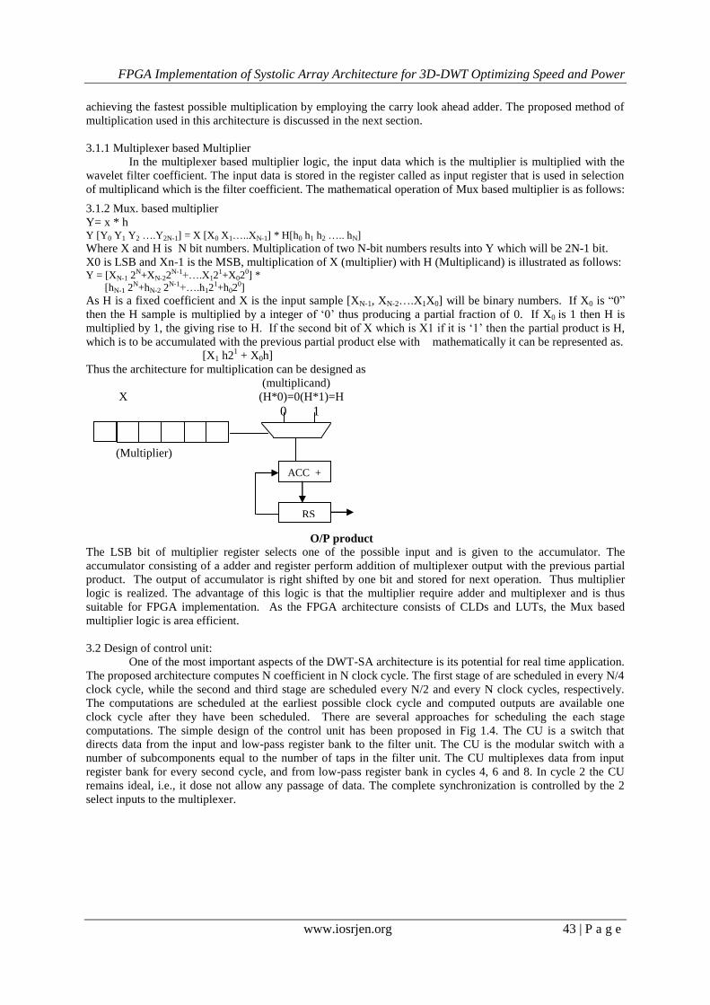
3.1.1 Multiplexer based Multiplier
In the multiplexer based multiplier logic, the input data which is the multiplier is multiplied with the
wavelet filter coefficient. The input data is stored in the register called as input register that is used in selection
of multiplicand which is the filter coefficient. The mathematical operation of Mux based multiplier is as follows:
3.1.2 Mux. based multiplier
Y= x * h Y [Y0 Y1 Y2 ….Y2N-1] = X [X0 X1…..XN-1] * H[h0 h1 h2 ….. hN]
Where X and H is N bit numbers. Multiplication of two N-bit numbers results into Y which will be 2N-1 bit.
X0 is LSB and Xn-1 is the MSB, multiplication of X (multiplier) with H (Multiplicand) is illustrated as follows: Y = [XN-1 2
N+XN-22N-1+….X12
1+X020] *
[hN-1 2N+hN-2 2
N-1+….h121+h02
0]
As H is a fixed coefficient and X is the input sample [XN-1, XN-2….X1X0] will be binary numbers. If X0 is “0”
then the H sample is multiplied by a integer of „0‟ thus producing a partial fraction of 0. If X0 is 1 then H is
multiplied by 1, the giving rise to H. If the second bit of X which is X1 if it is „1‟ then the partial product is H,
which is to be accumulated with the previous partial product else with mathematically it can be represented as.
[X1 h21 + X0h]
Thus the architecture for multiplication can be designed as
(multiplicand)
X (H*0)=0(H*1)=H
0 1
(Multiplier)
O/P product
The LSB bit of multiplier register selects one of the possible input and is given to the accumulator. The
accumulator consisting of a adder and register perform addition of multiplexer output with the previous partial
product. The output of accumulator is right shifted by one bit and stored for next operation. Thus multiplier
logic is realized. The advantage of this logic is that the multiplier require adder and multiplexer and is thus
suitable for FPGA implementation. As the FPGA architecture consists of CLDs and LUTs, the Mux based
multiplier logic is area efficient.
3.2 Design of control unit:
One of the most important aspects of the DWT-SA architecture is its potential for real time application.
The proposed architecture computes N coefficient in N clock cycle. The first stage of are scheduled in every N/4
clock cycle, while the second and third stage are scheduled every N/2 and every N clock cycles, respectively.
The computations are scheduled at the earliest possible clock cycle and computed outputs are available one
clock cycle after they have been scheduled. There are several approaches for scheduling the each stage
computations. The simple design of the control unit has been proposed in Fig 1.4. The CU is a switch that
directs data from the input and low-pass register bank to the filter unit. The CU is the modular switch with a
number of subcomponents equal to the number of taps in the filter unit. The CU multiplexes data from input
register bank for every second cycle, and from low-pass register bank in cycles 4, 6 and 8. In cycle 2 the CU
remains ideal, i.e., it dose not allow any passage of data. The complete synchronization is controlled by the 2
select inputs to the multiplexer.
ACC +
+
RS

FPGA Implementation of Systolic Array Architecture for 3D-DWT Optimizing Speed and Power
www.iosrjen.org 44 | P a g e

FPGA Implementation of Systolic Array Architecture for 3D-DWT Optimizing Speed and Power
www.iosrjen.org 45 | P a g e
3.3 Design of storage unit
In the proposed architecture three storage units are used:
1. Input Register Bank (RBI).
2. Low-pass Register Bank (RBL).
3. High-pass Register Bank (RBH).
The data register are used in these storage units.
3.3.1 RBI
The DWT equations (1a) and (1b) show that the value of the computed filter coefficient depends on the present
as well as the five previous data samples. It is therefore required that the present and past five input data values
Table 1.2 Continued
Tabl com R14 R15 R16 R17 R18 R19 R20 R21 R22 R23 R24 R25 R2
6
1 C(0)
2
3 C(2)
4
5 C(4)
6
7 C(6)
8
9 C(0)
10
11 C(2)
12 E(0)
13 C(4)
14
15 C(6)
16 E(4)
17 C(0)
18
19 C(2)
20 E(0)
21 C(4)
22
23 C(6)
24 E(4)
25 C(0)
26 E(0)
27 C(2) E(0)
28 E(0) E(0)
29 C(4) E(0)
30 E(4) E(0)
31 C(6) E(4) E(0)
32 E(4) E(4) E(0)
33 C(0) E(4) E(0)
34 E(0) E(4) E(0)
35 C(2) E(0) E(4) E(0)
36 E(0) E(0) E(4) E(0)
37 C(4) E(0) E(4) E(0)
38 G(4) E(4) E(0) E(4) E(0
)

FPGA Implementation of Systolic Array Architecture for 3D-DWT Optimizing Speed and Power
www.iosrjen.org 46 | P a g e
be held in registers and be retrieved by the FU and CU. Therefore, five registers are connected serially in a
chain, and at any clock cycle each register passes its contents to its right neighbor which results only in the five
past values being retained.
3.3.2 RBL & RBH
Several registers are required for storage of the intermediate partial results. 26 data registers are
required to implement register bank. The number of registers required in this architecture is directly proportional
to the number of levels of DWT decomposition, and is calculated during the construction of the timetable of the
computations. The allocation of the data into the register is employed by Forward Register Allocation (FRA)
method. This method is easy to implement, simpler, requires less control circuitry and permits easy adaptation
of the architecture for coefficient calculation of more than three stages. In this method the data moves
systolically in one direction only, hence the name FRA.
IV. FPGA IMPLEMENTATION OF SA-DWT Device utilization summary:
Selected Device : 2vp30ff896-7
Number of Slices: 6059 out of 13696 44%
Number of Slice Flip Flops: 5222 out of 27392 19%
Number of 4 input LUTs: 8025 out of 27392 29%
Number of bonded IOBs: 120 out of 556 21%
Number of GCLKs: 1 out of 16 6%
Minimum period: 6.248ns
(Maximum Frequency: 160.051MHz)
Minimum input arrival time before clock: 4.367ns
Maximum output required time after clock: 3.922ns
Parameters DA-
DWT
Modified
DA-DWT
SA-
DWT
No. of
Slices 9724 9528 6059
Power mW 33.62 36 32.4
Frequency
in MHz 112 145 160.051
V. DESIGN OF SA-DWT ARCHITECTURE FOR 3D DWT The 3D DWT can be considered as a combination of three 1D DWT in the x, y and z directions, as
shown in Figure.1.5. The preliminary work in the DWT processor design is to build 1D DWT modules, which
are composed of high-pass and low-pass filters that perform a convolution of filter coefficients and input pixels.
After a one-level of 3D discrete wavelet transform, the volume of frame data is decomposed into HHH, HHL,
HLH, HLL, LHH, LHL, LLH and LLL signals as shown in the Figure. 1.5.
H
H
H
H
L
L
L
L
L
H
L
H
L
H
Input
X(x,y,z)
HHH
HHL
HLH
HLL
LHH
LHL
LLL
High pass Component
Low Pass component
High pass Component
Low Pass component
High pass Component
Low Pass component
High pass Component
Low Pass component
2
2
2
2
2
2
2
2
2 High pass
Component
2 Low Pass component
2 High pass
Component
Low Pass Component
2 High pass
Component
2
Low Pass Component
2
L
H
L H
LL
LH
HL
HH
LLH
X - Direction Y - Direction Z - Direction
Figure 1.5 One-level 3D DWT structure (3) Figure 1.5 One-level 3D DWT structures [3]

FPGA Implementation of Systolic Array Architecture for 3D-DWT Optimizing Speed and Power
www.iosrjen.org 47 | P a g e
5.1 Proposed design
Design and VLSI implementation of high speed, low power 3D wavelet architecture is focused on
video coding application. Flexible hardware architecture is designed for performing 3D Discrete Wavelet
Transform. The proposed architecture uses new and fast lifting scheme which has the ability of performing
progressive computations by minimizing the buffering between the decomposition levels.
Video
frames (8X8X8)
L H LL HL
LH HH
LLL LLH HLL HLH
LHL LHH HHL HHH
Column Processing Temporal processing
Figure 1.6 Block diagram of 3D1 level DWT
decomposition
Figure 1.6 Block diagram of 3D 1 level DWT decomposition
Figure 1.7 Spatial and temporal sampling of a video sequence
VI. 3D SYSTOLIC ARRAY ARCHITECTURE The 2D systolic array architecture presented in previous section is extended in designing of 3D DWT
architecture. in the 3D architecture, each frame of size N x N is transformed independently using 2D DWT
systolic array architecture along the row and columns. The transformed matrix consisting of 4 sections of N/2 x
N/2 elements in each frame is further transformed using 1D DWT systolic array cell. In order to compute the 1D
DWT in the temporal direction, four systolic array cells shown in figure 1.2 and figure 1.4 are considered for 1D
computation. Figure below shows the data control operation for the 8 elements being transformed using 1D
Systolic array cell. There are 12 temporal registers that store the 8 pixels of each frame in the temporal direction.
Remaining four registers are used for symmetric extension of the 8 pixels. The LPF and HPF coefficients are
stored in the registers D. The control unit enables the data read operation for 8 pixels and filter coefficients, and
enables individual MAC unit for multiplication and addition. The intermediate samples computed are down
sampled by using a ½ rate clock. 8 pixels are decomposed into 4 low pass and 4 high pass representing sub
bands in the temporal domain. All the four systolic array architectures operate in the temporal domain parallel
thus computing the DWT in the temporal direction. The N x N x 8 video frame is decomposed into 8 sub bands
of N/2 x N/2 x 4. The computation of third level DWT is carried out in 8N clock cycles and thus has latency of
12 clock cycles and through put of 4 clock cycles.
Spatial
samples
Temporal
samples
y
x
y
z
x
y

FPGA Implementation of Systolic Array Architecture for 3D-DWT Optimizing Speed and Power
www.iosrjen.org 48 | P a g e
Intermediate Memory
For a 8x8x8 image, computation time for 2D DWT is 2 (64)+2(8)-1 clock cycles. As there are 8
frames, 8 parallel 1D-SADWT architecture perform DWT computation simultaneously. For each frame the
row wise as well as column wise computation is required. As there are 8 rows and the filter width is 8 for low
pass and 8 for high pass, computation of 1 output sample requires 16 clock cycler for low pass and high pass.
Thus for one row it requires 24 clock cycles. As there are 8 rows the total number of clock cycles is (24x8).
Similarly it requires (24x8) clock cycles for column computation. It is also requires to transform (8x8) row
output to 8x8 column output, hence is requires 64 clock cycles. Hence the total clock cycles for 2D DWT
computation is [(24x8)+(24x8) +64] clock cycles. As all the frames are processed in parallel, the time remains
same for 8 frame computation.
After computation of 2D DWT, each frame is divided into 4 sub images each of size 4*4. Thus before
computation of 3D DWT it is required to re arrange the output of 2D DWT as the LL of each frame has to be
stored in a single memory, and there are 8 LL component from each frame, it required (8x16) clock cycles for
rearrangement after rearrangement, of all 4 sub images 1D DWT is computed in the temporal directions, thus
as there are 8 pixels in temporal direction, it requires 16 clock cycles to compute LLL and LLH components.
There are four 1D DWT operating in the temporal direction and hence 8 sub bonds are computed. The total
time required to perform 1D DWT is the temporal direction is (8*4*4) clock cycles. The figure shows the 1D
DWT computations in temporal direction.
1D-SA DWT
LLL
LL
H
1
32

FPGA Implementation of Systolic Array Architecture for 3D-DWT Optimizing Speed and Power
www.iosrjen.org 49 | P a g e
The data flow diagram shown in Table 1.2 can be extended to represent the data flow for 3D DWT computation
by introducing four columns of register relocation columns for four independent DWT computations.
VII. FPGA IMPLEMENTATION OF SA-3DDWT In order to estimate the area, timing and power parameters for the proposed 3D DWT architecture
based on systolic array a video sequence of size 64 x 64 x 8 is considered as a reference image. The input data is
stored in 8 separate memories each of size 4096 x 8. The 2D DWT architecture is used to compute the DWT of
individual frames and the DWT output is reorganized and stored in four separate memory of size 8192 x 8. The
systolic array architecture for the third level (temporal domain) is used to compute the 3D DWT output and the
final results is stored in the output memory of size 4096 x 8. During third level DWT computation, new frames
are loaded into the input memory for 2D DWT computation. The memory control unit designed controls the
data flow operation between three different memory units. The HDL model for the 3D DWT is developed and
verified for its functionality using ModelSim. The verified design is synthesized using Xilinx ISE targeting
Virtex II pro FPGA. The synthesis report obtained is analyzed and the results are tabulated below. In order to
compare the performances of the proposed design, a generic HDL model for 3D DWT is developed,
functionally verified and is synthesized using Xilinx ISE. The generic model is considered as reference model
for comparison of performance parameters.
Parameter Reference SA-3D DWT
Number of slices 25864 15167
Maximum delay 82MHz 127 MHz
Maximum power 3.2 W 1.9 W
From the results obtained it is found that the systolic array architecture operates at 127 MHz of
frequency and consumes less power. Since memory reallocation technique is adopted, the size of intermediate
memory is reduced thus saving the total area for 3D DWT computation as compared with generic 3D DWT
model. In order to further improve the operating frequency, number of DWT computations in the temporal
domain can be increased from 4 to 8 thus choosing two temporal rows of 2D DWT matrices; this would increase
the area but will reduce delay.
VIII. CONCLUSION: In this paper, a modified architecture for 3D DWT is proposed, designed and implemented. The 2D
DWT systolic array architecture is extended to compute 3D DWT using four parallel 1D DWT architecture. The
number of registers in the third level DWT computation is reduced to array of 12 registers. The designed
hardware is implemented on Virtex II FPGAs and have been tested for its functionality. The proposed 3D DWT
is also developed using simulink environment, various test images have been considered for functional
verification. The systolic array design consisting of data processing logic, memory controllers and temporary
memory logic have bee modeled using HDL and simulated using Modelsim. The functionally correct model is
synthesized using Xilinx ISE and is implemented on FPGA. The performance results prove that the SA-DWT is
suitable for high speed and low power applications. The developed design can be used as an IP for image
transformation in medical and commercial applications. The design can be further improved by replacing the
multiplier and adder logic by high speed multipliers and adders. The 3D DWT can be further integrated with 3D
SPIHT for data compression.

FPGA Implementation of Systolic Array Architecture for 3D-DWT Optimizing Speed and Power
www.iosrjen.org 50 | P a g e
ACKNOWLEDGMENT The authors would like to thanks Dr. Cyril Prasanna Raj P , MS Ramaiah School of Advance studies,
Bangalore for his support.
REFERENCES [1]. Xuguang Lan and Nanning Zheng, proposed by “Low-Power And High-Speed VLSI Architecture For Lifting-Based
Forward And Inverse Wavelet Transform” , Consumer Electronics, IEEE Transactions Vol. 51 Issue: 2 pp.379-
385,July2005.
[2] Anirban Das, Anindya Hazra, and Swapna Banerjee “An Efficient Architecture for 3-D Discrete Wavelet
Transform”, IEEE Trans. Circuits and Systems for Video Technology Vol. 20 Issue: 2 pp.286-296,Feb.2010.
[3] Chin-Fa Hsieh , Tsung-Han Tsai , Neng-Jye Hsu , and Chih-Hung Lai , proposed “A novel, efficient VLSI
architecture for the implementation of one-dimension, lifting-based discrete wavelet transform (DWT)”, ICICIC '07
Proceedings of the Second International Conference on Innovative Computing, Information and IEEE Computer
Society Washington, DC, USA ©2007 table of contents ISBN:0-7695-2882-1 doi 10.1109/ICICIC.2007.346
[4]. Jen-Shiun Chiang, and Chih-Hsien Hsia have proposed “An Efficient VLSI Architecture for 2-D DWT using Lifting
Scheme”.IEEE Icss-2005 International conference on system and signals.pp.528-531.
[5]. Awad Kh. Al-Asmari and Abdulaziz Al-Rayes by “ A low bit rate three dimensional decomposition algorithm for
video compression with simple computational complexity is proposed”,Arabian journal for science and engineering
vol 29 Number 1B,april 2004.
[6]. M.F. L´opez, S.G. Rodr´ýguez, J.P. Ortiz, J.M. Dana, V.G. Ruiz and I. Garc´ýa have proposed “Fully Scalable Video
Coding with Packed Stream”.International Symp.on High performance computer architecture.
[7]. Malay Ranjan Tripathy, Kapil Sachdeva, and Rachid Talhi by “3D Discrete Wavelet Transform VLSI Architecture
for Image Processing”,Electromagnetics research symposium proceedings Moscow Russia,August 18-21 2009
[8]. Aroutchelvame,S.M. and K. Raahemifar by “An Efficient Architecture For Lifting-Based Forward And Inverse
Discrete Wavelet Transform”.multimedia and expo.2005,ICME 2005.IEEE international conference on pages 816-
819,july-,.1569 2005Amsterdam.
[9]. A.Daubechies, “The Wavelet Transform, time frequency, localization and signal analysis,” IEEE Transactions on
Info Theory, VOL 36, PP 961-1005.
[10]. F.Marino, V.Piuri, and Swartzlander, A parallel implementation of 2-D discrete wavelet transforms, IEEE trans
Signal Processing , Vol – 47 , pp 3179- 3184, nov 1999.
[11]. Baker, Li, Boyce , CMOS Circuit Design, Layout, and Simulation, IEEE Press, Prentice Hall India, second edition.
[12]. Marino, Two Fast Architectures for the Direct 2-D Discrete Wavelet Transform, IEEE Trans on signal Processing,
Vol 49, no.6 June 2001.
[13]. G.J. Hekstra “ Multiplier architecture for VLSI implementation” Deflt Univ Technology. The Netherlands Tech.
Rep.90-104. Nov1990
[14]. Y.LeCun and Y.Bengio. Multiplexer Based array Multipliers, IEEE transactions on Pattern Recognition, Vol .4 , Dec
2001.
[15]. G. Adiv. Determining three-dimensional motion and structure from optical flow generated by several moving
objects. IEEE Transaction on PAMI, vol. 7, no. 4, July 1985.
[16] . C. Chandrasekhar and S.Narayana Reddy, “ Desing of High speed, Low power 2D DWT for Video compression,”
journal of Innovation in Electronics and communication- Special issue.., vol.2(2), pp. 33-36, Jan-2012@ISSN 2249-
9946.
[17] . C. Chandrasekhar and S.Narayana Reddy, “Design of 3D-DWT Architecture using Systolic Array Based High Speed
1D –DWT,” The Conference on Computer Science & Computational Mathematics (CCSCM 2012), pp.88-96, 9-10
Feb, 2012, Melaka, Malaysia@ ISBN:978-0-615-59471-2.
[18]. C. Chandrasekhar and S.Narayana Reddy, “Dynamic Power Reduction in Modified Lifting Scheme Based DWT for
Image Processing” GJRE-F , , Electrical and Electronics Engineering pp.17-27, July, 2012 Volume 12 Issue 8
(Ver. 1.0) Online ISSN: 2249-4596 Print ISSN: 0975-5861.
[19]. C. Chandrasekhar and S. Narayana Reddy, “Performance Analysis of Modified Lifting Based DWT Architecture and
FPGA Implementation for Speed and Power” GJCST-F , Graphics & Vision , pp.41-50, Aug., 2012 Volume 12 Issue
12 (Ver. 1.0) Online ISSN : 0975-4172 Print ISSN : 0975-4350
Prof. C.Chandrasekhar received the B.E degree in Instrumentation Technology from
Govt.B.D.T.Collage of Engineering,Davanagere,Karnataka,India, in 1994, and the M.Tech. Degree in
Digital Electronics from B.V.B collage of Engineering ,Hubli,Karnataka,India in 2003.He is currently
working as Prof & HOD of Electronics & Communications Engineering Dept., Sree Venkateswara
College of Engineering & Technology, Chittoor, Andhra Pradesh, India. His Research interests include
signal and Image processing, VLSI architectures, complex system-on-chip design.
Dr. S.Narayana Reddy currently working as Professor and Head of Electronics & Communications
Engineering Dept.,S.V.University,Tirupathi. He has more than 25 years of Experience in teaching . He is
an expert in Digital Signal Processing. He has produced 3 PhD‟s and guiding 10 PhD scholars. He has
published more than 30 technical papers in national and International Journals and conferences. His
Research interests include multimedia and signal processing architecture, complex system-on-chip design.