freescale semiconductor, inc.cache.freescale.com/files/microcontrollers/doc/eng...• pipe increased...
TRANSCRIPT

EB376/DRev. 2, 11/2001
A comparison of theMC9S12DP256 (mask set0K36N) versus the HC12
Engineering Bulletin
F
ree
sca
le S
em
ico
nd
uc
tor,
I
Freescale Semiconductor, Inc.n
c..
.
By Joachim KrückenBEOS MCU DesignMunich/Germany© Motorola, Inc., 2001
For More Information On This Product, Go to: www.freescale.com

EB376/D Rev. 2
F
ree
sca
le S
em
ico
nd
uc
tor,
I
Freescale Semiconductor, Inc.n
c..
.
2 A Comparison of the MC9S12DP256 (Mask Set 0K36N) Versus the HC12 MOTOROLA
For More Information On This Product, Go to: www.freescale.com

EB376/D Rev. 2
F
ree
sca
le S
em
ico
nd
uc
tor,
I
Freescale Semiconductor, Inc.n
c..
.
Table of Contents
Table of Contents . . . . . . . . . . . . . . . . . . . . . . . . . . . . . . . . . . . . . . . . . . . . . . . . . . . . . 3
Introduction . . . . . . . . . . . . . . . . . . . . . . . . . . . . . . . . . . . . . . . . . . . . . . . . . . . . . . . . . 5Overview . . . . . . . . . . . . . . . . . . . . . . . . . . . . . . . . . . . . . . . . . . . . . . . . . . . . . . . 5Conventions Used Throughout This Document . . . . . . . . . . . . . . . . . . . . . . . . . . 5Module Base Addresses . . . . . . . . . . . . . . . . . . . . . . . . . . . . . . . . . . . . . . . . . . . 6
Central Processing Unit (CPU) . . . . . . . . . . . . . . . . . . . . . . . . . . . . . . . . . . . . . . . . . . 7Introduction . . . . . . . . . . . . . . . . . . . . . . . . . . . . . . . . . . . . . . . . . . . . . . . . . . . . . 7MOVB/MOVW instructions: . . . . . . . . . . . . . . . . . . . . . . . . . . . . . . . . . . . . . . . . . 7Instructions with cycle count reduced by 1 . . . . . . . . . . . . . . . . . . . . . . . . . . . . . 8Instructions with cycle count reduced by 2 . . . . . . . . . . . . . . . . . . . . . . . . . . . . . 8Instructions with cycle count increased by 1 . . . . . . . . . . . . . . . . . . . . . . . . . . . . 8Instructions with operations re-ordered . . . . . . . . . . . . . . . . . . . . . . . . . . . . . . . . 9
Hardware . . . . . . . . . . . . . . . . . . . . . . . . . . . . . . . . . . . . . . . . . . . . . . . . . . . . . . . . . . . 11Introduction . . . . . . . . . . . . . . . . . . . . . . . . . . . . . . . . . . . . . . . . . . . . . . . . . . . . 11Summary of Additional Functions on MC9S12DP256 . . . . . . . . . . . . . . . . . . . . 11MC9S12DP256 Power Supply Detail . . . . . . . . . . . . . . . . . . . . . . . . . . . . . . . . 13
EEPROM Memory . . . . . . . . . . . . . . . . . . . . . . . . . . . . . . . . . . . . . . . . . . . . . . . . . . . . 15EEPROM Memory . . . . . . . . . . . . . . . . . . . . . . . . . . . . . . . . . . . . . . . . . . . . . . . 15MC9S12DP256 Versus 68HC912DG128 . . . . . . . . . . . . . . . . . . . . . . . . . . . . . 15
Flash Memory . . . . . . . . . . . . . . . . . . . . . . . . . . . . . . . . . . . . . . . . . . . . . . . . . . . . . . . 17Flash Memory . . . . . . . . . . . . . . . . . . . . . . . . . . . . . . . . . . . . . . . . . . . . . . . . . . 17MC9S12DP256 Versus 68HC912DG128 . . . . . . . . . . . . . . . . . . . . . . . . . . . . . 17
Port Integration Module (PIM) . . . . . . . . . . . . . . . . . . . . . . . . . . . . . . . . . . . . . . . . . . 19Introduction . . . . . . . . . . . . . . . . . . . . . . . . . . . . . . . . . . . . . . . . . . . . . . . . . . . . 19I/O port configuration . . . . . . . . . . . . . . . . . . . . . . . . . . . . . . . . . . . . . . . . . . . . . 19
Clocks and Reset Generator (CRG) . . . . . . . . . . . . . . . . . . . . . . . . . . . . . . . . . . . . . 21Clocks and Reset Generator (CRG) . . . . . . . . . . . . . . . . . . . . . . . . . . . . . . . . . 21MC9S12DP256 Versus 68HC912DG128 . . . . . . . . . . . . . . . . . . . . . . . . . . . . . 21
Pulse Width Modulator (PWM) . . . . . . . . . . . . . . . . . . . . . . . . . . . . . . . . . . . . . . . . . 23Introduction . . . . . . . . . . . . . . . . . . . . . . . . . . . . . . . . . . . . . . . . . . . . . . . . . . . . 23Summary of Additional Functions on MC9S12DP256 . . . . . . . . . . . . . . . . . . . . 23Comparison of PWM Equations . . . . . . . . . . . . . . . . . . . . . . . . . . . . . . . . . . . . 23Register Block Comparison . . . . . . . . . . . . . . . . . . . . . . . . . . . . . . . . . . . . . . . . 25
MOTOROLA A Comparison of the MC9S12DP256 (Mask Set 0K36N) Versus the HC12 3
For More Information On This Product, Go to: www.freescale.com

EB376/D Rev. 2
F
ree
sca
le S
em
ico
nd
uc
tor,
I
Freescale Semiconductor, Inc.n
c..
.
Enhanced Capture Timer (ECT) . . . . . . . . . . . . . . . . . . . . . . . . . . . . . . . . . . . . . . . . 29Introduction . . . . . . . . . . . . . . . . . . . . . . . . . . . . . . . . . . . . . . . . . . . . . . . . . . . . 29Summary of Additional Functions on MC9S12DP256 . . . . . . . . . . . . . . . . . . . . 29Register Block Comparison . . . . . . . . . . . . . . . . . . . . . . . . . . . . . . . . . . . . . . . . 29
Serial Communications Interface (SCI) . . . . . . . . . . . . . . . . . . . . . . . . . . . . . . . . . . 31Introduction . . . . . . . . . . . . . . . . . . . . . . . . . . . . . . . . . . . . . . . . . . . . . . . . . . . . 31Summary of Additional Functions on MC9S12DP256 . . . . . . . . . . . . . . . . . . . . 31Register Block Comparison . . . . . . . . . . . . . . . . . . . . . . . . . . . . . . . . . . . . . . . . 32
Serial Peripheral Interface (SPI) . . . . . . . . . . . . . . . . . . . . . . . . . . . . . . . . . . . . . . . . 33Introduction . . . . . . . . . . . . . . . . . . . . . . . . . . . . . . . . . . . . . . . . . . . . . . . . . . . . 33Summary of Additional Functions on MC9S12DP256 . . . . . . . . . . . . . . . . . . . . 33Register Block Comparison . . . . . . . . . . . . . . . . . . . . . . . . . . . . . . . . . . . . . . . . 34
Inter-IC Bus (IIC) . . . . . . . . . . . . . . . . . . . . . . . . . . . . . . . . . . . . . . . . . . . . . . . . . . . . . 37Introduction . . . . . . . . . . . . . . . . . . . . . . . . . . . . . . . . . . . . . . . . . . . . . . . . . . . . 37Summary of Additional Functions on the MC9S12DP256 . . . . . . . . . . . . . . . . . 37Register Block Comparison . . . . . . . . . . . . . . . . . . . . . . . . . . . . . . . . . . . . . . . . 38
Motorola Scalable CAN (MSCAN) . . . . . . . . . . . . . . . . . . . . . . . . . . . . . . . . . . . . . . . 39Introduction . . . . . . . . . . . . . . . . . . . . . . . . . . . . . . . . . . . . . . . . . . . . . . . . . . . . 39Summary of Additional Functions on MC9S12DP256 . . . . . . . . . . . . . . . . . . . . 40Register Block Comparison . . . . . . . . . . . . . . . . . . . . . . . . . . . . . . . . . . . . . . . . 41
Analog-to-Digital Converter (ATD) . . . . . . . . . . . . . . . . . . . . . . . . . . . . . . . . . . . . . . 43Introduction . . . . . . . . . . . . . . . . . . . . . . . . . . . . . . . . . . . . . . . . . . . . . . . . . . . . 43Summary of Additional Functions on MC9S12DP256 . . . . . . . . . . . . . . . . . . . . 43Register Block Comparison . . . . . . . . . . . . . . . . . . . . . . . . . . . . . . . . . . . . . . . . 45
Byte Data Link Controller (BDLC) . . . . . . . . . . . . . . . . . . . . . . . . . . . . . . . . . . . . . . . 53Introduction . . . . . . . . . . . . . . . . . . . . . . . . . . . . . . . . . . . . . . . . . . . . . . . . . . . . 53Summary of Additional Functions on MC9S12DP256 . . . . . . . . . . . . . . . . . . . . 53Register Block Comparison . . . . . . . . . . . . . . . . . . . . . . . . . . . . . . . . . . . . . . . . 54
Background Debug Module (BDM) . . . . . . . . . . . . . . . . . . . . . . . . . . . . . . . . . . . . . . 57Introduction . . . . . . . . . . . . . . . . . . . . . . . . . . . . . . . . . . . . . . . . . . . . . . . . . . . . 57Summary of Additional Functions on MC9S12DP256 . . . . . . . . . . . . . . . . . . . . 57Register Block Comparison . . . . . . . . . . . . . . . . . . . . . . . . . . . . . . . . . . . . . . . . 58Breakpoint registers . . . . . . . . . . . . . . . . . . . . . . . . . . . . . . . . . . . . . . . . . . . . . . 58
4 A Comparison of the MC9S12DP256 (Mask Set 0K36N) Versus the HC12 MOTOROLA
For More Information On This Product, Go to: www.freescale.com

EB376/D Rev. 2Overview
F
ree
sca
le S
em
ico
nd
uc
tor,
I
Freescale Semiconductor, Inc.n
c..
.
Introduction
Overview
This document compares the various modules of the MC9S12DP256 (mask0K36N) with equivalent modules in the HC12 family and is meant to be used asa guide in conjunction with the appropriate device Data Books.
It is structured (where possible) to align with the Chapter structure of theMC9S12DP256 Technical Data Book, MC9S12DP256/D.
Generally, the first subsection of each chapter highlights the differences infeatures of the two devices. Where appropriate, this is followed by acomparison of the individual registers and bits.
The HCS12 (MC9S12DP256) design methodology includes a greatly improvedhighly flexible I/O structure. On the HC12, port control is managed by registerbits in the appropriate peripheral modules. On the MC9S12DP256, thefunctionality of these bits has been greatly expanded and centralized in thePort Integration Module (PIM).
Conventions Used Throughout This Document
In the register comparisons, the bits highlighted in bold italics indicate thedifferences between the corresponding registers of the devices beingcompared.
Registers not identified remain identical.
Port I/O control bits are not included in the register comparisons as theirfunctionality has been transferred to the PIM. For detail on the I/O philosophyand Port registers refer to the Port Integration Module (PIM) chapter in thisdocument and in the MC9S12DP256 Technical Data Book, MC9S12DP256/D.
MOTOROLA A Comparison of the MC9S12DP256 (Mask Set 0K36N) Versus the HC12 5
For More Information On This Product, Go to: www.freescale.com

EB376/D Rev. 2
F
ree
sca
le S
em
ico
nd
uc
tor,
I
Freescale Semiconductor, Inc.n
c..
.
Module Base Addresses
The following table lists the base addresses for each module on theMC9S12DP256 and their equivalent on the 68HC912DG128 (or 68HC912B32in the case of the BDLC module).
Table 1Module Base Addresses
ModuleBase Address
68HC912DG128 MC9S12DP256
BKPT $20 $28
CRG (CGM) $34 $34
ECT $80 $40
ATD0 $60 $80
PWM $40 $A0
SCI0 $C0 $C8
SCI1 $C8 $D0
SPI0 $D0 $D8
IIC $E0 $E0
BDLC$F8 (on 68HC912B32 not
68HC912DG128)$E8
SPI1 — $F0
SPI2 — $F8
Flash $F4 $100
EEPROM $F0 $110
ATD1 $1E0 $120
MSCAN0 $100 $140
MSCAN1 $300 $180
MSCAN2 — $1C0
MSCAN3 — $200
PIM — $240
MSCAN4 — $280
BDM $FF00 $FF00
6 A Comparison of the MC9S12DP256 (Mask Set 0K36N) Versus the HC12 MOTOROLA
For More Information On This Product, Go to: www.freescale.com

EB376/D Rev. 2Introduction
F
ree
sca
le S
em
ico
nd
uc
tor,
I
Freescale Semiconductor, Inc.n
c..
.
Central Processing Unit (CPU)
Introduction
• Identical programmers model.
• Pipe increased to 3 stages (from 2 plus latch) giving deterministicbehavior.
• All instructions implemented using same Mnemonics & Op codes.
• Further detail can be found in the HCS12 CPU Reference Guide.
MOVB/MOVW instructions:
On the HC12, when using the PC relative addressing mode, an offset isrequired to be added to/subtracted from the displacement computed fromthe base address, which is equal to the address of the next instruction. Thisis detailed in chapter 3.9.1 of the CPU12 Reference Manual (CPU12M/AD).It is handled transparently by assemblers and compilers for the HC12 today.
On the HCS12 this is no longer the case. This base is the same for bothsource and destination operands and any assemblers/compilers thatcalculate an offset will generate incorrect code.
Examples
MOVB2,PCR,$1000DC.B1,2,3,4,5,6,7,8,9
HCS12: $1000 is written to 3HC12: $1000 is written to 1
The other way round
MOVB$1000,2,PCRTEMPDS.B 10
HCS12: Value read at $1000 is moved to TEMP+2HC12: Value read at $1000 is moved to TEMP+5
It is important to ensure that a compiler or assembler is HCS12 compliant onthis point.
MOTOROLA A Comparison of the MC9S12DP256 (Mask Set 0K36N) Versus the HC12 7
For More Information On This Product, Go to: www.freescale.com

EB376/D Rev. 2
F
ree
sca
le S
em
ico
nd
uc
tor,
I
Freescale Semiconductor, Inc.n
c..
.
Instructions with cycle count reduced by 1
BRCLR IDX1BRSET IDX1CALL EXT, IDX, IDX1, IDX2 (7,7,7,8)CLR [D,IDX], [IDX2]STAA [D,IDX], [IDX2]STAB [D,IDX], [IDX2]STD [D,IDX], [IDX2]STS [D,IDX], [IDX2]STX [D,IDX], [IDX2]STY [D,IDX], [IDX2]STOP INH (entering)TRAP INH (mapped to multiple op codes)WAI INH (entering)
Instructions with cycle count reduced by 2
BRCLR IDX2
BRSET IDX2
MUL INH
TBL IDX
Instructions with cycle count increased by 1
RTC INH
RTI INH (with pending interrupt)
STOP INH (exiting)
WAI INH (interrupt occurs)
NOTE: The increase in RTC is compensated for by the reduction in the number ofcycles in the CALL instruction. Effective throughput is the same number ofcycles except CALL IDX2, RTC.
8 A Comparison of the MC9S12DP256 (Mask Set 0K36N) Versus the HC12 MOTOROLA
For More Information On This Product, Go to: www.freescale.com

EB376/D Rev. 2Instructions with operations re-ordered
F
ree
sca
le S
em
ico
nd
uc
tor,
I
Freescale Semiconductor, Inc.n
c..
.
Instructions with operations re-ordered
In order to make the cycle by cycle operation the same for similarinstructions, the free cycle "f" has been moved to the last operation (133cases). [Pf at end of instruction = even number of cycles]
In order to make the cycle by cycle operation the same for similarinstructions, the optional program word fetch cycle "O" has been moved tothe last operation (72 cases). [PO at the end of instruction = odd number ofcycles]
In 14 other cases the cycle by cycle sequence has been modified to end inthe program word fetch "P" (no "f" or "O" cycles in instructions).
A total of 219 cycle order changes have been made in the CPU operation.These should be transparent for most applications.
MOTOROLA A Comparison of the MC9S12DP256 (Mask Set 0K36N) Versus the HC12 9
For More Information On This Product, Go to: www.freescale.com

EB376/D Rev. 2
F
ree
sca
le S
em
ico
nd
uc
tor,
I
Freescale Semiconductor, Inc.n
c..
.
10 A Comparison of the MC9S12DP256 (Mask Set 0K36N) Versus the HC12 MOTOROLA
For More Information On This Product, Go to: www.freescale.com

EB376/D Rev. 2Introduction
F
ree
sca
le S
em
ico
nd
uc
tor,
I
Freescale Semiconductor, Inc.n
c..
.
Hardware
Introduction
The MC9S12DP256 has many more (multiplexed) peripheral modules than the68HC912DG128 and a significantly different power supply structure to cater forit’s low voltage, high performance 0.25µ core logic and 5V compatible, highlyflexible I/O ports.
This requires a different printed circuit board (PCB) layout.
Hybrid layouts, supporting both foot prints, can be achieved using acombination of jumpers, pull-up/down resistors and solderable links but theseare likely to result in significant compromises in performance and EMC.
This section compares the PCB requirements of the MC9S12DP256 with thoseof the 68HC912DG128. The first section highlights the differences in features,including some considerations on power supply layout and decoupling.
Summary of Additional Functions on MC9S12DP256
• ATDVRL and VRH voltage reference input
The MC9S12DP256 requires a single ATD voltage reference input andreference ground pin shared by both converters as opposed to theseparate reference connections for each converter on the68HC912DG128.
• Pin out changes and Package details
The mechanical package is identical (112 pin LQFP, Case 987) to the68HC912DG128 but many pins with equivalent functionality havechanged location.
• ATD channel convention
On the MC9S12DP256, the channels for ATD1 are referred to in thedocumentation by AN08–AN15 instead of AN10–AN17 as on the68HC912DG128. This gives clear and consistent channel numberingfrom 00 on up allowing for future implementations of converters withgreater than 8 input channels.
Physically, the channels of ATD1 (AN08–AN15) remain interlaced withthe channels of ATD0 (AN00–AN07) as on the 68HC912DG128 but theirlocation relative to pin 1 has moved.
MOTOROLA A Comparison of the MC9S12DP256 (Mask Set 0K36N) Versus the HC12 11
For More Information On This Product, Go to: www.freescale.com

EB376/D Rev. 2
F
ree
sca
le S
em
ico
nd
uc
tor,
I
Freescale Semiconductor, Inc.n
c..
.
• EXTAL pin
The oscillator is part of the higher frequency logic, hence EXTAL inputis limited to 2.5V signals.
• XTAL pin
The XTAL output can be buffered with a high-impedance buffer to drivethe EXTAL input of another device. On the MC9S12DP256, themaximum output voltage of this pin is VDDPLL (2.5V).
• Port K
The MC9S12DP256 has 6 pins on Port K to support 64 x 16K pages ofexternal memory (1 Mbyte).
• VSTBY pin
There is no RAM standby function on the MC9S12DP256, so the VSTBYpin has been removed.
• MODC pin
Previously referred to as SMODN, this is for factory test only. The pincontinues to act as the background debug pin in user applications.
• TEST pin
This is a ‘factory-test’ only input and MUST be grounded or pulled toground with a pull-down resistor in all other applications.
• ECLK output
ECLK control is significantly different. Please refer to the Port E andPEAR register sections of the MC9S12DP256 Technical Data Book,MC9S12DP256/D for details.
• Port E7 pin
On the MC9S12DP256, the alternate functionality of this pin haschanged – (CAL function not available, *ECLK not available, *DBE notavailable). Pulling PE7 (*XCLKS) low during the reset phase bypassesthe internal low current oscillator and an internal buffer (2.5V) driven byEXTAL feeds the internal clocks.
• Port K7 pin.
On the MC9S12DP256, this pin is used as an emulation chip selectsignal for the emulation of the internal memory expansion or as generalpurpose I/O, depending upon the state of the EMK bit in the MODEregister.
The value on this pin during reset determines the state of the ROMONbit during reset into all expanded modes.
12 A Comparison of the MC9S12DP256 (Mask Set 0K36N) Versus the HC12 MOTOROLA
For More Information On This Product, Go to: www.freescale.com

EB376/D Rev. 2MC9S12DP256 Power Supply Detail
F
ree
sca
le S
em
ico
nd
uc
tor,
I
Freescale Semiconductor, Inc.n
c..
.
• Flash programming voltage
On the MC9S12DP256, the non-volatile Flash memory is ‘5V only’ anddoes not require an external VFP Pin as on the 68HC912DG128; thisremoves the need for an external charge pump.
MC9S12DP256 Power Supply Detail
The MC9S12DP256 has an internal 2.5V regulator to supply the highperformance core logic as opposed to the 5V only logic supply of the68HC912DG128. Some key points are highlighted here, but it is essential thatthe Voltage Regulator (VREG) Chapter of the MC9S12DP256 Technical DataBook be reviewed in detail.
• VREGEN Pin
I/P used to define the standby operating mode of the internal voltageregulator.
• VDD1 & VDD2 Pins
2.5V supply pins for the core logic which require decoupling.
• VDDPLL Pin
On the 68HC912DG128, this pin, when grounded, caused the PLLcircuitry to be bypassed. On the MC9S12DP256, it is a 2.5V (internal)supply pin for the high performance PLL logic and must NOT begrounded (or connected to 5V).
• Layout considerations
Avoid current loops in power supply tracks.All ground pins (VSS**) must be connected externally.VDDA/VSSA and VRH/VRL supplies MUST be clean.Connection for external power supply monitor should be close to VDDA.
• Further Decoupling Guidelines
For all capacitors in the nF range, it is essential to use a type with lowESR.All recommendations are load and PC board routing dependent.– VDDX
This is highly dependent on the type of load and switching frequencysince VDDX supplies only the 5V drivers in Ports J, K, T, P, M & S.
Start with 47–220nF and add 10µF if big loads are switched and thesupply track is long (highly inductive).All fast switching peripherals, PWM, timer, CAN etc. are located onthis bus.
MOTOROLA A Comparison of the MC9S12DP256 (Mask Set 0K36N) Versus the HC12 13
For More Information On This Product, Go to: www.freescale.com

EB376/D Rev. 2
F
ree
sca
le S
em
ico
nd
uc
tor,
I
Freescale Semiconductor, Inc.n
c..
.
– VDDA
Here a good noise decoupling is key; the internal load is almoststatic.Recommended 22nF–100nF.
– VDD1,2
These are the outputs of the internal voltage regulator.Recommended 47–220nF.
– VDDR
This pin supplies the internal regulator as well as the I/O ports A, B,E & H.Two alternatives:
a. Expanded busHigh peak current through Port A, B, E mainly.Recommended 100nF + 10uF.
b. Single chip mode.Here we have a load dependent variant. Since the are no fastswitching peripherals on this supply relatively slow switchingoutputs under software control assumed.Recommended 100nF if no big loads on the output.If higher output currents are required, add 1µF – 10µF.
– VDDPLL
The most important point here is decoupling of the high frequencynoise generated by the oscillator and PLL switching.Recommended 22nF – 100nF.
– VRH & VRL
This is the reference for the ADT convertor so it must be a ‘clean’supply.Recommended 10nF, high frequency.
14 A Comparison of the MC9S12DP256 (Mask Set 0K36N) Versus the HC12 MOTOROLA
For More Information On This Product, Go to: www.freescale.com

EB376/D Rev. 2EEPROM Memory
F
ree
sca
le S
em
ico
nd
uc
tor,
I
Freescale Semiconductor, Inc.n
c..
.
EEPROM Memory
EEPROM Memory
A new EEPROM technology has been implemented on the MC9S12DP256which differs completely from the 68HC912DG128. It is recommended that theappropriate sections of the MC9S12DP256 Technical Data Book,MC9S12DP256/D, should be read and understood before attempting any codeconversions.
The 4Kbyte EEPROM module is arranged in a 2048 by 16-bit configuration andmay be read as bytes, aligned words or misaligned words. Write operations forprogram or erase are only allowed as aligned word accesses. An erased wordreads $FFFF.
A command state machine has been added to the flash block to simplify theprogram and erase algorithms.
It is not possible to read from the EEPROM array while it is being programmedor erased.
The base addresses for the EEPROM registers are as follows:
MC9S12DP256 Versus 68HC912DG128
• New register block.
• ECLKDIV register used to supply the command state machine with aclock reference between 150 and 200 KHz, from the extal inputreference.
• EEPROM size increased to 4Kbytes from 2Kbytes.
• Aligned word programmable only, no longer byte programmable.
• Minimum erase sector size 4 bytes, compared to byte erasable.
• The command state machine can generate interrupts, thereforeprogramming and erase routines can be interrupt driven.
68HC912DG128 MC9S12DP256
$F0 $110
MOTOROLA A Comparison of the MC9S12DP256 (Mask Set 0K36N) Versus the HC12 15
For More Information On This Product, Go to: www.freescale.com

EB376/D Rev. 2
F
ree
sca
le S
em
ico
nd
uc
tor,
I
Freescale Semiconductor, Inc.n
c..
.
• A configurable protected area is available. The size of the protected areacan be set from 0 to 512 bytes in multiples of 64 bytes. The EPROT(EEPROM protection) register is preloaded out of reset with a valuestored in EEPROM.
16 A Comparison of the MC9S12DP256 (Mask Set 0K36N) Versus the HC12 MOTOROLA
For More Information On This Product, Go to: www.freescale.com

EB376/D Rev. 2Flash Memory
F
ree
sca
le S
em
ico
nd
uc
tor,
I
Freescale Semiconductor, Inc.n
c..
.
Flash Memory
Flash Memory
A new flash technology has been implemented on the MC9S12DP256 whichdiffers completely from the 68HC912DG128. It is recommended that theappropriate sections of the MC9S12DP256 Technical Data Book,MC9S12DP256/D, should be read and understood before attempting any codeconversions.
The 256Kbyte flash module is comprised of four 64Kbyte blocks. Each 64Kbyteblock is arranged in a 32K by 16-bit configuration and may be read as bytes,aligned words or misaligned words. Write operations for program or erase areonly allowed as aligned word accesses. An erased word reads $FFFF.
A command state machine has been added to the flash block to simplify theprogram and erase algorithms.
The base addresses for the Flash registers are as follows:
MC9S12DP256 Versus 68HC912DG128
• New register block.
• FCLKDIV register used to supply the command state machine with aclock reference between 150 and 200 KHz, from the extal inputreference.
• Flash size increased to 256Kbytes from 128Kbytes.
• No requirement for an external programming voltage, VFP pin removed.
• Aligned word programmable only, no longer byte programmable.
• Erase sector size 512 bytes, bulk erase also available, compared to bulkerase only.
• All four blocks can be programmed and erased in parallel.
• The command state machine can generate interrupts, thereforeprogramming and erase routines can be interrupt driven.
68HC912DG128 MC9S12DP256
$F4 $100
MOTOROLA A Comparison of the MC9S12DP256 (Mask Set 0K36N) Versus the HC12 17
For More Information On This Product, Go to: www.freescale.com

EB376/D Rev. 2
F
ree
sca
le S
em
ico
nd
uc
tor,
I
Freescale Semiconductor, Inc.n
c..
.
• Two configurable protected areas within each 64 Kbyte block. One areacan be configured as a 0.5, 1, 2 or 4 Kbyte protected block, the other asa 2, 4, 8 or 16 Kbyte protected block.
• One 64 Kbyte block contains all the information relating to security andthe protected areas within the entire 256 Kbytes. The FPROT (Flashprotection) and FSEC (Flash security) registers are preloaded out ofreset with the values stored in flash, there is also an additional eightbytes used as a security backdoor comparison key.
• Improved write/erase cycle performance.
18 A Comparison of the MC9S12DP256 (Mask Set 0K36N) Versus the HC12 MOTOROLA
For More Information On This Product, Go to: www.freescale.com

EB376/D Rev. 2Introduction
F
ree
sca
le S
em
ico
nd
uc
tor,
I
Freescale Semiconductor, Inc.n
c..
.
Port Integration Module (PIM)
Introduction
The MC9S12DP256 has an extremely flexible I/O structure which is centrallyconfigured in the Port Integration Module (PIM) providing a high level ofmultiplexed functionality on pins.
The PIM provides two basic functions
• Arbitration of which module has control of the pads for a givenconfiguration, i.e. which module is allowed to drive the pads and in whatdirection at any one time.
Each module takes control in turn according to an assigned priority.
• Defines the "electrical" characteristics where appropriate for each pin.
Those are:– reduced drive– wired-or mode (more accurately open-drain mode)– pull-ups/downs. Here certain precautions are taken, such as if the
CAN is enabled pull-up is allowed, but pull-down is blocked.
The 68HC912DG128 port control was more limited and controlled by individualregister bits in the appropriate peripheral modules with limited sharing of I/Ofunctions.
The base addresses for the PIM registers are as follows:
I/O port configuration
On the MC9S12DP256 each port has a set of control registers (in the PIM)arranged in a similar structure where each individual I/O pin can be configuredfor:
• Input/output selection
• Drive strength reduction
• Enable and select of pull resistors
• Interrupt enable and status flags
68HC912DG128 MC9S12DP256
— $240
MOTOROLA A Comparison of the MC9S12DP256 (Mask Set 0K36N) Versus the HC12 19
For More Information On This Product, Go to: www.freescale.com
EB376/D Rev. 2
F
ree
sca
le S
em
ico
nd
uc
tor,
I
Freescale Semiconductor, Inc.n
c..
.
A standard port has the following minimum features:
• Input/output selection
• 5V output drive with two selectable drive strengths
• 5V digital and analog input
• Input with selectable pull-up or pull-down device
Optional features:
• Open drain for wired-or connections
• Interrupt inputs with glitch filtering
Port Input Registers can be used to detect overload or short circuit conditionson output pins.
Refer to the external pin description section of the MC9S12DP256 TechnicalData Book, MC9S12DP256/D, for further details.
20 A Comparison of the MC9S12DP256 (Mask Set 0K36N) Versus the HC12 MOTOROLA
For More Information On This Product, Go to: www.freescale.com
EB376/D Rev. 2Clocks and Reset Generator (CRG)
F
ree
sca
le S
em
ico
nd
uc
tor,
I
Freescale Semiconductor, Inc.n
c..
.
Clocks and Reset Generator (CRG)
Clocks and Reset Generator (CRG)
The CRG module provides system clock generation and is responsible foroscillator, phase locked loop (PLL), real time interrupt (RTI) and computeroperating properly (COP) watchdog control.
The CRG replaces the Clock Generator Module (CGM) found on the68HC912DG128 and although they both provide similar functionality, the CRGshould be considered as a new module.
This section is intended to highlight the differences between the CRG andCGM, but due to the complexity and importance of this module it isrecommended that the appropriate sections of the MC9S12DP256 TechnicalData Book, MC9S12DP256/D, should be read and understood beforeattempting any code conversions.
The base addresses for the CRG registers are as follows:
MC9S12DP256 Versus 68HC912DG128
• Restructured register block.
• Maximum bus speed increased to 25 MHz (extal 50 MHz) from 8MHz(extal 16MHz).
• If extal is driven by an external clock source then the signal amplitudeswing MUST be limited between VSS and VDDPLL (2.5 Volts).
• VDDPLL is no longer used as a logic level when exiting reset. It isinternally generated from an onboard VREG and under nocircumstances should it be connected to VSS.
• The reset state of PE7 (not XCLKS) can be used to bypass the oscillatorwhen using an external clock signal to drive extal (PE7 = VSS).
• Self Clock Mode (SCM) is a terminology change from Limp Home Mode.
• The startup counter, used by the crystal monitor to check for properoscillator startup recovery has been changed to a 14-stage (8192cycles) from a 13-stage (4096 cycles) counter.
68HC912DG128 MC9S12DP256
(CGM) $34 $34
MOTOROLA A Comparison of the MC9S12DP256 (Mask Set 0K36N) Versus the HC12 21
For More Information On This Product, Go to: www.freescale.com

EB376/D Rev. 2
F
ree
sca
le S
em
ico
nd
uc
tor,
I
Freescale Semiconductor, Inc.n
c..
.
• COP is disabled out of reset in normal modes, the time-out rates havechanged.
• RTI rates have been enhanced offering increased flexibility.
• The SLOW MODE divide feature on the 68HC912DG128 has beenremoved.
• Increased control over PLL functionality.
• Internal resets hold the reset pin low for 128 SYSCLK cycles, the resetpin is then sampled a further 64 cycles later to determine whether thereset source is internal or external. In comparison the 68HC912DG128asserts the reset pin low for 16 ECLK cycles and then samples a further9 cycles later.
22 A Comparison of the MC9S12DP256 (Mask Set 0K36N) Versus the HC12 MOTOROLA
For More Information On This Product, Go to: www.freescale.com
EB376/D Rev. 2Introduction
F
ree
sca
le S
em
ico
nd
uc
tor,
I
Freescale Semiconductor, Inc.n
c..
.
Pulse Width Modulator (PWM)
Introduction
This section compares the PWM module of the MC9S12DP256 with that of the68HC912DG128.
The base addresses for the PWM registers are as follows:
Summary of Additional Functions on MC9S12DP256
• Expanded to eight full channels.
• Independent justification control of all channels.
• Emergency shutdown
An Emergency shutdown function has been incorporated into theMC9S12DP256. If the emergency shutdown function is enabled and portP bit 7 becomes active, all enabled PWM output channels areimmediately driven to the level defined by PWMLVL in the PWMSDNregister.
• Expanded I/O Pin control (ref Port Integration Module (PIM))
Comparison of PWM Equations
PWM Scalingequations
68HC912DG128 Clock S0 = Clock A / (2 * (PWSCAL0 + 1))Clock S1 = Clock B / (2 * (PWSCAL1 + 1))
MC9S12DP256 Clock SA = Clock A / (2 * PWMSCLA)Clock SB = Clock B / (2 * PWMSCLB)
68HC912DG128 MC9S12DP256
$40 $A0
MOTOROLA A Comparison of the MC9S12DP256 (Mask Set 0K36N) Versus the HC12 23
For More Information On This Product, Go to: www.freescale.com

EB376/D Rev. 2
F
ree
sca
le S
em
ico
nd
uc
tor,
I
Freescale Semiconductor, Inc.n
c..
.
PWM PeriodEquations
68HC912DG128 Left Aligned OutputPeriod = [Channel-Clock-Period * (PWPER + 1)]
Centre Aligned OutputPeriod = [Channel-Clock-Period * (2 * PWPER)]
MC9S12DP256 Left Aligned OutputPWMx Period = Channel Clock Period * PWMPERx
Center Aligned OutputPWMx Period = Channel Clock Period * (2 * PWMPERx)
24 A Comparison of the MC9S12DP256 (Mask Set 0K36N) Versus the HC12 MOTOROLA
For More Information On This Product, Go to: www.freescale.com
EB376/D Rev. 2Register Block Comparison
F
ree
sca
le S
em
ico
nd
uc
tor,
I
Freescale Semiconductor, Inc.n
c..
.
Register Block Comparison
Symbolic names have been modified from PWxx to PWMxx. Software equatesshould be adjusted to suit.
The greatest changes to the MC9S12DP256 PWM register map occur due tothe expansion of the PWM from four to eight modulators. The additionalmodulator control registers PWMCNT4–7, PWMPER4–7, PWMDTY4–7 andreorganization of PWME, PWMPOL, PWMCLK, PWMPRCLK, PWMCAE, andPWMCTL facilitate this addition.
PWM EnableRegister:
PWME7..0 — PWM Enable Bits
PWM channel enabled. The pulse modulated signal becomes available atPWM output line when its clock source begins its next cycle.
Address offset: $02
0 0 0 0 PWEN3 PWEN2 PWEN1 PWEN0
Reset: 0 0 0 0 0 0 0 0
68HC912DG128 – PWEN
Address offset: $00
PWME7 PWME6 PWME5 PWME4 PWME3 PWME2 PWME1 PWME0
Reset: 0 0 0 0 0 0 0 0
MC9S12DP256 – PWME
MOTOROLA A Comparison of the MC9S12DP256 (Mask Set 0K36N) Versus the HC12 25
For More Information On This Product, Go to: www.freescale.com

EB376/D Rev. 2
F
ree
sca
le S
em
ico
nd
uc
tor,
I
Freescale Semiconductor, Inc.n
c..
.
PWM PolarityRegister and ClockSelect Register:
PPOL7..0 — PWM Enable Bits
If set, PWM channel output is high at the beginning of the period, then goeslow when the duty count is reached.
PCLK7..0 — PWM Clock Select Bits
The PWM clock select bits, which were contained in the upper nibble of thePWPOL, register are now in a dedicated PWMCLK register.
Address offset: $01
PCLK3 PCLK2 PCLK1 PCLK0 PPOL3 PPOL2 PPOL1 PPOL0
Reset: 0 0 0 0 0 0 0 0
68HC912DG128 – PWPOL
Address offset: $01
PPOL7 PPOL6 PPOL5 PPOL4 PPOL3 PPOL2 PPOL1 PPOL0
Reset: 0 0 0 0 0 0 0 0
MC9S12DP256 – PWMPOL
Address offset: $02
PCLK7 PCLK6 PCLK5 PCLK4 PCLK3 PCLK2 PCLK1 PCLK0
Reset: 0 0 0 0 0 0 0 0
MC9S12DP256 – PWMCLK
26 A Comparison of the MC9S12DP256 (Mask Set 0K36N) Versus the HC12 MOTOROLA
For More Information On This Product, Go to: www.freescale.com

EB376/D Rev. 2Register Block Comparison
F
ree
sca
le S
em
ico
nd
uc
tor,
I
Freescale Semiconductor, Inc.n
c..
.
PWM Prescale ClockSelect Registers:
PCKA2..0, PCKB2..0 — PWM Prescale A and B Clock Select Bits
The PWM prescale clock select bits, which were contained in the PWCLKregister, are now in a dedicated PWMPRCLK register. Notice that the bitdefinitions have moved as well.
CON67, 45, 23, 01 – Concatenation Control Select Bits
The concatenation control bits have been increased for the additionalchannels and moved to the PWMCTL register.
Address offset: $00
CON23 CON01 PCLKA2 PCLKA1 PCLKA0 PCLKB2 PCLKB1 PCLKB0
Reset: 0 0 0 0 0 0 0 0
68HC912DG128 – PWCLK
Address offset: $03
0 PCKB2 PCKB1 PCKB0 0 PCKA2 PCKA1 PCKA0
Reset: 0 0 0 0 0 0 0 0
MC9S12DP256 – PWMPRCLK
Address offset: $05
CON67 CON45 CON23 CON01 PSWAI PFRZ 0 0
Reset: 0 0 0 0 0 0 0 0
MC9S12DP256 – PWMCTL
MOTOROLA A Comparison of the MC9S12DP256 (Mask Set 0K36N) Versus the HC12 27
For More Information On This Product, Go to: www.freescale.com

EB376/D Rev. 2
F
ree
sca
le S
em
ico
nd
uc
tor,
I
Freescale Semiconductor, Inc.n
c..
.
PWM ControlRegisters(continued)
PSWAI — PWM Stops in Wait Mode
The PSWAI bit has be moved from the 5th bit position to the 4th position inthe PWMCNT register.
PFRZ — PWM Counters Stop in Freeze Mode
The PFRZ bit has been added to disable the PWM input clock to theprescaler whenever the part is in freeze (background) mode. This is usefulfor emulation.
CAE7..0 — PWM Center Align Enable Select Bits
Independent control of channel justification is now available in a dedicatedPWMCAE register. In the 68HC912DG128, all channels were controlledcollectively by one bit, CENTR, but in the MC9S12DP256, each channel canbe justified individually by its own CAE bit.
Address offset: $14
0 0 0 PSWAI CENTR RDPP PUPP PSBCK
Reset: 0 0 0 0 0 0 0 0
68HC912DG128 – PWCTL
Address offset: $05
CON67 CON45 CON23 CON01 PSWAI PFRZ 0 0
Reset: 0 0 0 0 0 0 0 0
MC9S12DP256 – PWMCTL
Address offset: $04
CAE7 CAE6 CAE5 CAE4 CAE3 CAE2 CAE1 CAE0
Reset: 0 0 0 0 0 0 0 0
MC9S12DP256 – PWMCAE
28 A Comparison of the MC9S12DP256 (Mask Set 0K36N) Versus the HC12 MOTOROLA
For More Information On This Product, Go to: www.freescale.com

EB376/D Rev. 2Introduction
F
ree
sca
le S
em
ico
nd
uc
tor,
I
Freescale Semiconductor, Inc.n
c..
.
Enhanced Capture Timer (ECT)
Introduction
The enhanced capture timer can be used for generating periodic pulses (outputcompare), time measurements (e.g. measure of a pulse frequency or measurebetween two occurred pulse events – input capture), counting the number oftimes an event occurs (using a pulse accumulator) or to generate a periodicinterrupt (using the modulus down counter).
This section compares the ECT module of the MCS912DP256 with that of the68HC912DG128.
The base addresses for the ECT registers are as follows:
Summary of Additional Functions on MC9S12DP256
• Toggle on overflow
The MC9S12DP256 can be configured to toggle output compare pins ontimer overflow. This feature is enabled using a new register.
• Expanded I/O Pin control (ref Port Integration Module (PIM))
Register Block Comparison
Timer Toggle OnOverflow Register1(TTOV):
This register has been added to the MC9S12DP256. It gives the user additionalcontrol over the I/O pins in output compare mode.
TOVx — Toggle On Overflow Bits
TOVx toggles output compare pin on overflow. This feature only takes effectwhen in output compare mode. When set, it takes precedence over forcedoutput compare but not channel 7 override events.
68HC912DG128 MC9S12DP256
$80 $40
Address offset: $07
TOV7 TOV6 TOV5 TOV4 TOV3 TOV2 TOV1 TOV0
Reset: 0 0 0 0 0 0 0 0
MCS912DP256 – TTOV
MOTOROLA A Comparison of the MC9S12DP256 (Mask Set 0K36N) Versus the HC12 29
For More Information On This Product, Go to: www.freescale.com

EB376/D Rev. 2
F
ree
sca
le S
em
ico
nd
uc
tor,
I
Freescale Semiconductor, Inc.n
c..
.
Timer SystemControl Register 1(TSCR1)
TSCR1 was called TSCR in the 68HC912DG128.
TSFRZ
Timer and Modulus Counter Stop while in Freeze (background) Mode.
Timer SystemControl Register 2(TSCR2)
TSCR2 was called TMSK2 in the 68HC912DG128.
Timer InterruptEnable Register 1(TIE)
TIE was called TMSK1 in the 68HC912DG128.
Address offset: $06
TEN TSWAI TSBCK TFFCA 0 0 0 0
Reset: 0 0 0 0 0 0 0 0
68HC912DG128 – TSCR
Address offset: $06
TEN TSWAI TSFRZ TFFCA 0 0 0 0
Reset: 0 0 0 0 0 0 0 0
MC9S12DP256 – TSCR1
Address offset: $0D
TOI 0 PUPT RDPT TCRE PR2 PR1 PR0
Reset: 0 0 0 0 0 0 0 0
68HC912DG128 – TMSK2
Address offset: $0D
TOI 0 0 0 TCRE PR2 PR1 PR0
Reset: 0 0 0 0 0 0 0 0
MC9S12DP256 – TSCR2
Address offset: $0C
C7I C6I C5I C4I C3I C2I C1I C0I
Reset: 0 0 0 0 0 0 0 0
30 A Comparison of the MC9S12DP256 (Mask Set 0K36N) Versus the HC12 MOTOROLA
For More Information On This Product, Go to: www.freescale.com
EB376/D Rev. 2Introduction
F
ree
sca
le S
em
ico
nd
uc
tor,
I
Freescale Semiconductor, Inc.n
c..
.
Serial Communications Interface (SCI)
Introduction
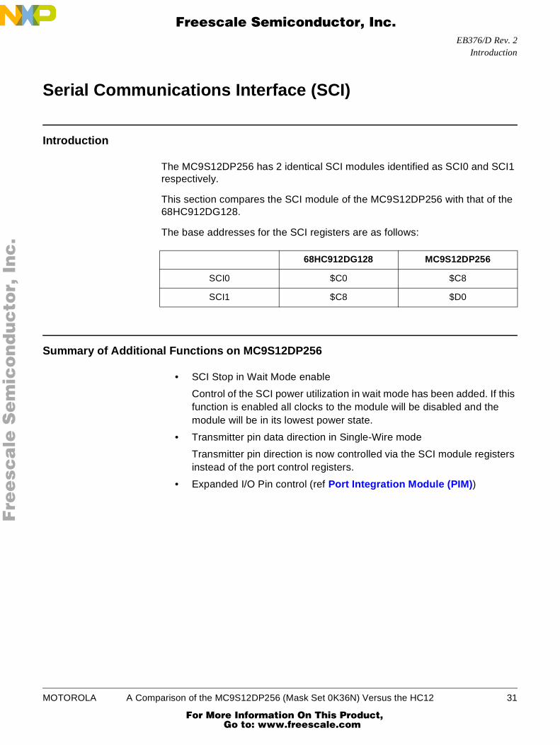
The MC9S12DP256 has 2 identical SCI modules identified as SCI0 and SCI1respectively.
This section compares the SCI module of the MC9S12DP256 with that of the68HC912DG128.
The base addresses for the SCI registers are as follows:
Summary of Additional Functions on MC9S12DP256
• SCI Stop in Wait Mode enable
Control of the SCI power utilization in wait mode has been added. If thisfunction is enabled all clocks to the module will be disabled and themodule will be in its lowest power state.
• Transmitter pin data direction in Single-Wire mode
Transmitter pin direction is now controlled via the SCI module registersinstead of the port control registers.
• Expanded I/O Pin control (ref Port Integration Module (PIM))
68HC912DG128 MC9S12DP256
SCI0 $C0 $C8
SCI1 $C8 $D0
MOTOROLA A Comparison of the MC9S12DP256 (Mask Set 0K36N) Versus the HC12 31
For More Information On This Product, Go to: www.freescale.com
EB376/D Rev. 2
F
ree
sca
le S
em
ico
nd
uc
tor,
I
Freescale Semiconductor, Inc.n
c..
.
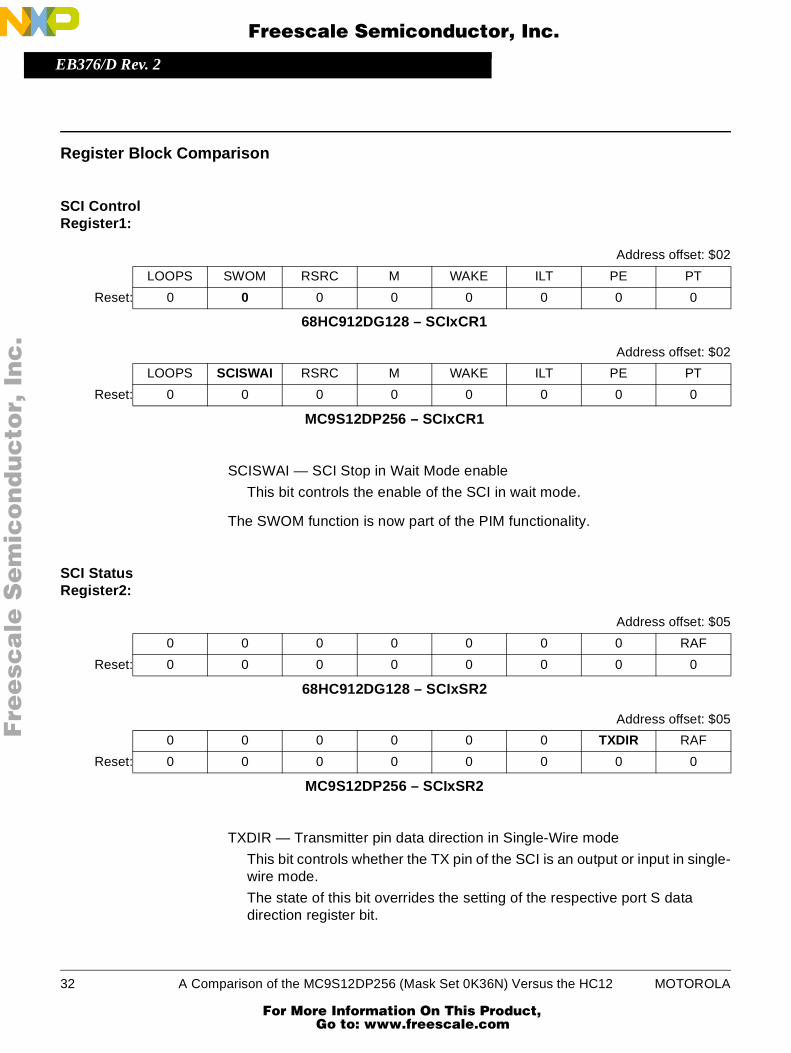
Register Block Comparison
SCI ControlRegister1:
SCISWAI — SCI Stop in Wait Mode enable
This bit controls the enable of the SCI in wait mode.
The SWOM function is now part of the PIM functionality.
SCI StatusRegister2:
TXDIR — Transmitter pin data direction in Single-Wire mode
This bit controls whether the TX pin of the SCI is an output or input in single-wire mode.
The state of this bit overrides the setting of the respective port S datadirection register bit.
Address offset: $02
LOOPS SWOM RSRC M WAKE ILT PE PT
Reset: 0 0 0 0 0 0 0 0
68HC912DG128 – SCIxCR1
Address offset: $02
LOOPS SCISWAI RSRC M WAKE ILT PE PT
Reset: 0 0 0 0 0 0 0 0
MC9S12DP256 – SCIxCR1
Address offset: $05
0 0 0 0 0 0 0 RAF
Reset: 0 0 0 0 0 0 0 0
68HC912DG128 – SCIxSR2
Address offset: $05
0 0 0 0 0 0 TXDIR RAF
Reset: 0 0 0 0 0 0 0 0
MC9S12DP256 – SCIxSR2
32 A Comparison of the MC9S12DP256 (Mask Set 0K36N) Versus the HC12 MOTOROLA
For More Information On This Product, Go to: www.freescale.com

EB376/D Rev. 2Introduction
F
ree
sca
le S
em
ico
nd
uc
tor,
I
Freescale Semiconductor, Inc.n
c..
.
Serial Peripheral Interface (SPI)
Introduction
The MC9S12DP256 has 3 identical SPI modules identified as SPI0, SPI1 andSPI2 respectively.
This section compares the SPI module of the MC9S12DP256 with that of the68HC912DG128.
The base addresses for the SPI registers are as follows:
Summary of Additional Functions on MC9S12DP256
• Baud rate Control
The SPI baud rate register has three additional bits that pre-scale themodule clock allowing greater baud rate selection possibilities.
• 16 bit transfers
An idle master or idle slave that has no data loaded into its transmitbuffer allows the user to queue up 16-bit values to send.
• SPI0 may be defined to operate in wired-or mode.
• Expanded I/O Pin control (ref Port Integration Module (PIM))
68HC912DG128 MC9S12DP256
SPI0 $D0 $D8
SPI1 — $F0
SPI2 — $F8
MOTOROLA A Comparison of the MC9S12DP256 (Mask Set 0K36N) Versus the HC12 33
For More Information On This Product, Go to: www.freescale.com

EB376/D Rev. 2
F
ree
sca
le S
em
ico
nd
uc
tor,
I
Freescale Semiconductor, Inc.n
c..
.
Register Block Comparison
SPI ControlRegister1:
SPTIE — SPI Transmit Interrupt Enable
This bit enables an SPI interrupt to be generated each time the SPTEF flagis set.
The SWOM function is now part of the PIM functionality.
SPI Baud RateRegister:
SPPR2..0 — SPI Baud Rate Pre-selection Bits
The baud rate divisor equation is as follows:
BaudRateDivisor = (SPPR +1) *2(SPR+ 1)
The additional bits allow pre-scaling of the module clock to compensate forincreased clock rates.
Address offset: $00
SPIE SPE SWOM MSTR CPOL CPHA SSOE LSBFE
Reset: 0 0 0 0 0 1 0 0
68HC912DG128 – SPxCR1
Address offset: $00
SPIE SPE SPTIE MSTR CPOL CPHA SSOE LSBFE
Reset: 0 0 0 0 0 1 0 0
MC9S12DP256 – SPIxCR1
Address offset: $02
0 0 0 0 0 SPR2 SPR1 SPR0
Reset: 0 0 0 0 0 0 0 0
68HC912DG128 – SPxBR
Address offset: $02
0 SPPR2 SPPR1 SPPR0 0 SPR2 SPR1 SPR0
Reset: 0 0 0 0 0 1 0 0
MC9S12DP256 – SPIxBR
34 A Comparison of the MC9S12DP256 (Mask Set 0K36N) Versus the HC12 MOTOROLA
For More Information On This Product, Go to: www.freescale.com

EB376/D Rev. 2Register Block Comparison
F
ree
sca
le S
em
ico
nd
uc
tor,
I
Freescale Semiconductor, Inc.n
c..
.
SPI Status Register:
SPIF — SPI Interrupt Flag
This bit is set after a received data byte has been transferred into the SPIData Register. This bit is cleared by reading the SPISR register (with SPIFset) followed by a read access to the SPI Data Register.
1 = New data copied into the SPIDR0 = Transfer not yet complete
The clearing mechanism of this bit has been changed. In the previous versionthe bit was cleared by reading the SPISR (with SPIF set) followed by readingor writing the SPI Data Register.
The write collision status flag has been removed.
SPTEF — SPI Transmit Empty Interrupt Flag
This bit is set each time the transmit data register transfers a byte into thetransmit register.
The write collision status flag has been removed.
Address offset: $03
SPIF WCOL 0 MODF 0 0 0 0
Reset: 0 0 0 0 0 0 0 0
68HC912DG128 – SPxSR
Address offset: $03
SPIF 0 SPTEF MODF 0 0 0 0
Reset: 0 0 1 0 0 0 0 0
MC9S12DP256 – SPIxSR
MOTOROLA A Comparison of the MC9S12DP256 (Mask Set 0K36N) Versus the HC12 35
For More Information On This Product, Go to: www.freescale.com
EB376/D Rev. 2
F
ree
sca
le S
em
ico
nd
uc
tor,
I
Freescale Semiconductor, Inc.n
c..
.
36 A Comparison of the MC9S12DP256 (Mask Set 0K36N) Versus the HC12 MOTOROLA
For More Information On This Product, Go to: www.freescale.com

EB376/D Rev. 2Introduction
F
ree
sca
le S
em
ico
nd
uc
tor,
I
Freescale Semiconductor, Inc.n
c..
.
Inter-IC Bus (IIC)
Introduction
The Inter-IC Bus (IIC or I2C) is a two-wire, bidirectional serial bus that providesa simple, efficient method of data exchange between devices. Being a two-wiredevice, the IIC Bus minimizes the need for large numbers of connectionsbetween devices, and eliminates the need for an address decoder.
This section compares the IIC module of the MC9S12DP256 to the IIC moduleof the 68HC912DG128.
The base addresses for the IIC registers are as follows:
Summary of Additional Functions on the MC9S12DP256
• The number of programmable serial clock frequencies has increasedfrom 64 (68HC912DG128) to 256 (MC9S12DP256).
• IBIF flag requires writing a "0" to clear. The 68HC912DG128 requires a"1".
• Expanded I/O Pin control (ref Port Integration Module (PIM))
68HC912DG128 MC9S12DP256
$E0 $E0
MOTOROLA A Comparison of the MC9S12DP256 (Mask Set 0K36N) Versus the HC12 37
For More Information On This Product, Go to: www.freescale.com

EB376/D Rev. 2
F
ree
sca
le S
em
ico
nd
uc
tor,
I
Freescale Semiconductor, Inc.n
c..
.
Register Block Comparison
IIC Bus FrequencyDivider Register:
IBC7–IBC0 — IIC Bus Clock Rate 7–0
This field is used to prescale the clock for bit rate selection. The bit clockgenerator is implemented as a prescaled shift register. IBC7–3 select theprescaler divider and IBC2-0 select the shift register tap point. Two additionbits, IBC[7:6], have been added to the MC9S12DP256, which provide anadditional divider factor to increase the number of programmable clockfrequencies to 256.
Address offset: $01
0 0 IBC5 IBC4 IBC3 IBC2 IBC1 IBC0
Reset: 0 0 0 0 0 0 0 0
68HC912DG128 – IBFD
Address offset: $01
IBC7 IBC6 IBC5 IBC4 IBC3 IBC2 IBC1 IBC0
Reset: 0 0 0 0 0 0 0 0
MC9S12DP256 – IBFD
38 A Comparison of the MC9S12DP256 (Mask Set 0K36N) Versus the HC12 MOTOROLA
For More Information On This Product, Go to: www.freescale.com

EB376/D Rev. 2Introduction
F
ree
sca
le S
em
ico
nd
uc
tor,
I
Freescale Semiconductor, Inc.n
c..
.
Motorola Scalable CAN (MSCAN)
Introduction
The MSCAN module is a serial messaging interface designed to communicateon a Controller Area Network (CAN) communication bus. The moduleimplements the CAN 2.0 A/B protocol as defined in the BOSCH specificationdated September 1991.
The MC9S12DP256 has 5 identical MSCAN modules identified as CAN0 toCAN4, each with its own RxCAN and TxCAN pins.
This section compares the MSCAN module of the MC9S12DP256 with that ofthe 68HC912DG128. The first section highlights the difference in features ofthe two devices.
The functionality of the MSCAN module has changed from previous HC12designs to the MC9S12DP256 version. Most of the changes are additions to thefunctionality, but a few are changes to the way that user software interacts withthe MSCAN module. One other major difference with the MC9S12DP256 is thatis has 5 MSCAN modules on board.
Refer to Motorola Application Note AN2011/D and the MC9S12DP256Technical Data Book, MC9S12DP256/D, for a detailed description of all of thechanges to the memory map, registers, control bits and other details of the newMSCAN module.
The base addresses for the MSCAN registers are as follows:
68HC912DG128 MC9S12DP256
MSCAN0 $100 $140
MSCAN1 $300 $180
MSCAN2 — $1C0
MSCAN3 — $200
MSCAN4 — $280
MOTOROLA A Comparison of the MC9S12DP256 (Mask Set 0K36N) Versus the HC12 39
For More Information On This Product, Go to: www.freescale.com
EB376/D Rev. 2
F
ree
sca
le S
em
ico
nd
uc
tor,
I
Freescale Semiconductor, Inc.n
c..
.
Summary of Additional Functions on MC9S12DP256
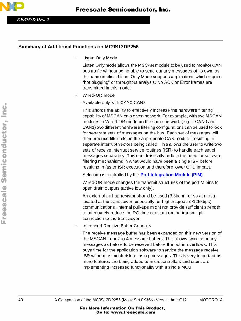
• Listen Only Mode
Listen Only mode allows the MSCAN module to be used to monitor CANbus traffic without being able to send out any messages of its own, asthe name implies. Listen Only Mode supports applications which require“hot plugging” or throughput analysis. No ACK or Error frames aretransmitted in this mode.
• Wired-OR mode
Available only with CAN0-CAN3
This affords the ability to effectively increase the hardware filteringcapability of MSCAN on a given network. For example, with two MSCANmodules in Wired-OR mode on the same network (e.g. – CAN0 andCAN1) two different hardware filtering configurations can be used to lookfor separate sets of messages on the bus. Each set of messages willthen produce filter hits on the appropriate CAN module, resulting inseparate interrupt vectors being called. This allows the user to write twosets of receive interrupt service routines (ISR) to handle each set ofmessages separately. This can drastically reduce the need for softwarefiltering mechanisms in what would have been a single ISR beforeresulting in faster ISR execution and therefore lower CPU impact.
Selection is controlled by the Port Integration Module (PIM).
Wired-OR mode changes the transmit structures of the port M pins toopen drain outputs (active low only).
An external pull-up resistor should be used (3.3kohm or so at most),located at the transceiver, especially for higher speed (>125kbps)communications. Internal pull-ups might not provide sufficient strengthto adequately reduce the RC time constant on the transmit pinconnection to the transciever.
• Increased Receive Buffer Capacity
The receive message buffer has been expanded on this new version ofthe MSCAN from 2 to 4 message buffers. This allows twice as manymessages as before to be received before the buffer overflows. Thisbuys time for the application software to service the message receiveISR without as much risk of losing messages. This is very important asmore features are being added to microcontrollers and users areimplementing increased functionality with a single MCU.
40 A Comparison of the MC9S12DP256 (Mask Set 0K36N) Versus the HC12 MOTOROLA
For More Information On This Product, Go to: www.freescale.com

EB376/D Rev. 2Register Block Comparison
F
ree
sca
le S
em
ico
nd
uc
tor,
I
Freescale Semiconductor, Inc.n
c..
.
• Message Buffer Time Stamping
The new MSCAN module contains a time stamping feature fortransmitted and received messages. This feature utilizes an internal 16-bit timer in the MSCAN module and places the timer value into apreviously reserved two-byte segment of the active message bufferwhen a message is transmitted or received and the timer is active.
• The five MSCAN modules on the MC9S12DP256 share pins withseveral other modules, namely Port M, Port J[7:6], Key Wakeup PinsKWJ[7:6], and the Inter-IC (IIC) Bus module.
• Expanded I/O Pin control now handled by the Port Integration Module(PIM), including prioritization of access to pins by active modules. ThePIM arbitrates between modules sharing pin resources. Please refer tothe Port Integration Module (PIM) section for more details.
Register Block Comparison
Please refer to AN2011/D for a detailed description of all of the changes to thememory map, registers, control bits and other details of the new MSCANmodule.
MOTOROLA A Comparison of the MC9S12DP256 (Mask Set 0K36N) Versus the HC12 41
For More Information On This Product, Go to: www.freescale.com

EB376/D Rev. 2
F
ree
sca
le S
em
ico
nd
uc
tor,
I
Freescale Semiconductor, Inc.n
c..
.
42 A Comparison of the MC9S12DP256 (Mask Set 0K36N) Versus the HC12 MOTOROLA
For More Information On This Product, Go to: www.freescale.com

EB376/D Rev. 2Introduction
F
ree
sca
le S
em
ico
nd
uc
tor,
I
Freescale Semiconductor, Inc.n
c..
.
Analog-to-Digital Converter (ATD)
Introduction
The MC9S12DP256 has 2 identical ATD modules identified as ATD0 andATD1 respectively. With the exception of the VDDA &VSSA (analog supplyvoltage) and VRH & VRL (analog conversion reference) all other pins areduplicated for each module.
The ATD module is an 8-Channel, 10-bit, multiplexed input, successiveapproximation, analog to digital converter accurate to ± 1LSB.
This section compares the ATD module of the MC9S12DP256 with that of the68HC912DG128.
The base addresses for the ATD registers are as follows:
Summary of Additional Functions on MC9S12DP256
• External triggering
The MC9S12DP256 has an additional external triggering function thatallows the user to synchronize the ATD conversion process with externalevents. The device can be configured to trigger on edges or levels ofdifferent polarities. Register ATDxCTL2 controls this function.
• External Trigger Input Pin
This pin is multiplexed with the CH7 input and is used to provide anexternal trigger input signal for the device when it is used in externaltrigger mode.
• Conversion sequence length
The MC9S12DP256 allows additional control over the number ofconversions in a sequence. In the 68HC912DG128, the user has achoice of 4 or 8 conversions depending on the S8CM control bit in theATDxCTL5 control register. However, in the MC9S12DP256 device, thenumber of conversions is controlled by a binary value in the ATDxCTL3control resister.
68HC912DG128 MC9S12DP256
ATD0 $60 $80
ATD1 $1E0 $120
MOTOROLA A Comparison of the MC9S12DP256 (Mask Set 0K36N) Versus the HC12 43
For More Information On This Product, Go to: www.freescale.com

EB376/D Rev. 2
F
ree
sca
le S
em
ico
nd
uc
tor,
I
Freescale Semiconductor, Inc.n
c..
.
• FIFO Mode
The MC9S12DP256 allows the user to select between different resultregister assignments in a conversion sequence. The reset state isidentical to the 68HC912DG128 in that the first result converted is storedin the first register, the second result in the second etc. However, anadditional FIFO mode is available that changes the registerassignments. In this mode, the results are placed in consecutiveregisters between conversion sequences. The result registers mappingwraps around when the end of the register file is reached. RegisterATDxCTL2 controls this function.
• Data justification
The MC9S12DP256 allows the user to control the justification (left orright) of the result that is stored into the data registers. The justificationdepends on the resolution that is selected. Register ATDxCTL5 controlsthis function.
• Signed/Unsigned control
The MC9S12DP256 allows the user to control if the data that is storedin the result registers is signed or unsigned. Register ATDxCTL5controls this function.
• Multichannel Conversion
The MC9S12DP256 allows the user additional flexibility when using themulti-channel conversions function. The user can configure the deviceto sample across several channels. The number of channels sampled iscontrolled by the S8C–S1C bits in the ATDxCTL3 register. The firstchannel sampled is determined by the state of the CC, CB and CA bitsin the ATDxCTL5 register.
• Analog/Digital Input Pin Multiplexing
The MC9S12DP256 has an Input Enable Mask register that allows theuser to individually enable each digital input buffer. This multiplexingfeature gives the user greater control. Register ATDDIEN controls thisfunction.
• Expanded I/O Pin control (ref Port Integration Module (PIM))
44 A Comparison of the MC9S12DP256 (Mask Set 0K36N) Versus the HC12 MOTOROLA
For More Information On This Product, Go to: www.freescale.com

EB376/D Rev. 2Register Block Comparison
F
ree
sca
le S
em
ico
nd
uc
tor,
I
Freescale Semiconductor, Inc.n
c..
.
Register Block Comparison
ATD ControlRegister 2:
.
ETRIGE – External Trigger Mode enable
This bit controls the enable of the external trigger mode.
ETRIGP – External Trigger Polarity control
This bit controls the polarity of the external trigger signal.
ETRIGLE – External Trigger Level/Edge control
This bit controls the mode of the incoming external trigger signal.
Reset Condition
Out of Reset the external trigger mode, on the MC9S12DP256, is disabled.Operation is identical to the 68HC912DG128.
Address offset: $02
ADPU AFFC ASWAI 0 0 0 ASCIE ASCIF
Reset: 0 0 0 0 0 0 0 0
68HC912DG128 – ATDxCTL2
Address offset: $02
ADPU AFFC ASWAI ETRIGLE ETRIGP ETRIGE ASCIE ASCIF
Reset: 0 0 0 0 0 0 0 0
MC9S12DP256 – ATDxCTL2
MOTOROLA A Comparison of the MC9S12DP256 (Mask Set 0K36N) Versus the HC12 45
For More Information On This Product, Go to: www.freescale.com

EB376/D Rev. 2
F
ree
sca
le S
em
ico
nd
uc
tor,
I
Freescale Semiconductor, Inc.n
c..
.
ATD ControlRegister 3:
S8C/S4C/S2C/S1C – Conversion Sequence Length
These bits represent a binary value, which is the length of the conversionsequence. The conversion sequence length coding table in the ATDxCTL3register description in the MC9S12DP256 Technical Data Book lists thecoding combinations.
FIFO – Result register FIFO mode
This bit determines if the result registers map to the conversion sequence.
Reset Condition
Out of Reset the conversion length sequence is set to 4 and the FIFO modeis disabled. This operation identical to the 68HC912DG128.
Address offset: $03
0 0 0 0 0 0 FRZ1 FRZ0
Reset: 0 0 0 0 0 0 0 0
68HC912DG128 – ATDxCTL3
Address offset: $03
0 S8C S4C S2C S1C FIFO FRZ1 FRZ0
Reset: 0 0 1 0 0 0 0 0
MC9S12DP256 – ATDxCTL3
46 A Comparison of the MC9S12DP256 (Mask Set 0K36N) Versus the HC12 MOTOROLA
For More Information On This Product, Go to: www.freescale.com
EB376/D Rev. 2Register Block Comparison
F
ree
sca
le S
em
ico
nd
uc
tor,
I
Freescale Semiconductor, Inc.n
c..
.
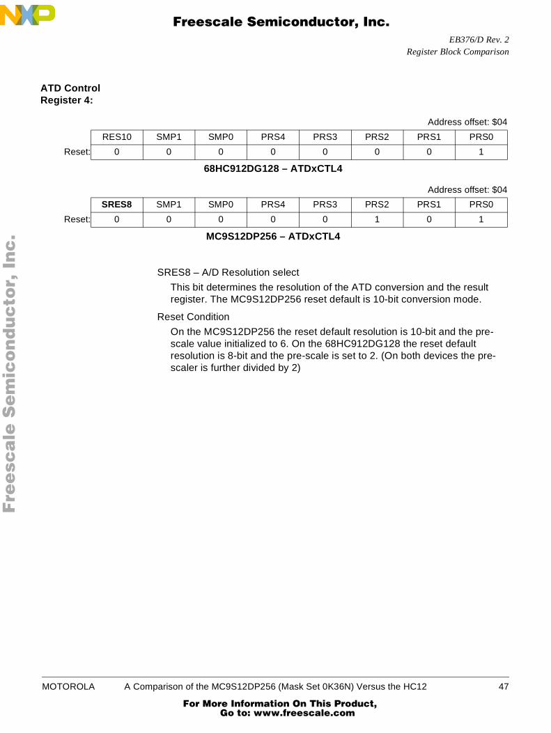
ATD ControlRegister 4:
SRES8 – A/D Resolution select
This bit determines the resolution of the ATD conversion and the resultregister. The MC9S12DP256 reset default is 10-bit conversion mode.
Reset Condition
On the MC9S12DP256 the reset default resolution is 10-bit and the pre-scale value initialized to 6. On the 68HC912DG128 the reset defaultresolution is 8-bit and the pre-scale is set to 2. (On both devices the pre-scaler is further divided by 2)
Address offset: $04
RES10 SMP1 SMP0 PRS4 PRS3 PRS2 PRS1 PRS0
Reset: 0 0 0 0 0 0 0 1
68HC912DG128 – ATDxCTL4
Address offset: $04
SRES8 SMP1 SMP0 PRS4 PRS3 PRS2 PRS1 PRS0
Reset: 0 0 0 0 0 1 0 1
MC9S12DP256 – ATDxCTL4
MOTOROLA A Comparison of the MC9S12DP256 (Mask Set 0K36N) Versus the HC12 47
For More Information On This Product, Go to: www.freescale.com
EB376/D Rev. 2
F
ree
sca
le S
em
ico
nd
uc
tor,
I
Freescale Semiconductor, Inc.n
c..
.
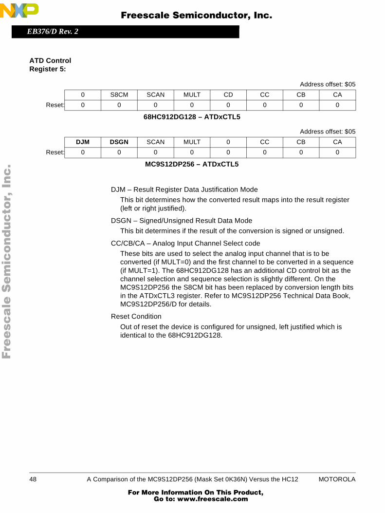
ATD ControlRegister 5:
DJM – Result Register Data Justification Mode
This bit determines how the converted result maps into the result register(left or right justified).
DSGN – Signed/Unsigned Result Data Mode
This bit determines if the result of the conversion is signed or unsigned.
CC/CB/CA – Analog Input Channel Select code
These bits are used to select the analog input channel that is to beconverted (if MULT=0) and the first channel to be converted in a sequence(if MULT=1). The 68HC912DG128 has an additional CD control bit as thechannel selection and sequence selection is slightly different. On theMC9S12DP256 the S8CM bit has been replaced by conversion length bitsin the ATDxCTL3 register. Refer to MC9S12DP256 Technical Data Book,MC9S12DP256/D for details.
Reset Condition
Out of reset the device is configured for unsigned, left justified which isidentical to the 68HC912DG128.
Address offset: $05
0 S8CM SCAN MULT CD CC CB CA
Reset: 0 0 0 0 0 0 0 0
68HC912DG128 – ATDxCTL5
Address offset: $05
DJM DSGN SCAN MULT 0 CC CB CA
Reset: 0 0 0 0 0 0 0 0
MC9S12DP256 – ATDxCTL5
48 A Comparison of the MC9S12DP256 (Mask Set 0K36N) Versus the HC12 MOTOROLA
For More Information On This Product, Go to: www.freescale.com

EB376/D Rev. 2Register Block Comparison
F
ree
sca
le S
em
ico
nd
uc
tor,
I
Freescale Semiconductor, Inc.n
c..
.
ATD Status RegisterHigh:
ETORF – External Trigger Overrun Flag
This flag is associated with edge trigger mode option. It is set if additionalactive edges are detected during a conversion sequence.
FIFOR – FIFO over Run Flag
This bit indicates that a result register has been written to before itsassociated conversion complete flag has been cleared.
Reset Condition
Out of reset the register is identical to the 68HC912DG128.
ATD Test ModuleTest Register High:
The registers are identical apart from the reset condition of SAR9.
Address offset: $06
SCF 0 0 0 0 C2 C1 C0
Reset: 0 0 0 0 0 0 0 0
68HC912DG128 – ATDxSTAT0
Address offset: $06
SCF 0 ETORF FIFOR 0 C2 C1 C0
Reset: 0 0 0 0 0 0 0 0
MC9S12DP256 – ATDxSTAT0
Address offset: $08
SAR9 SAR8 SAR7 SAR6 SAR5 SAR4 SAR3 SAR2
Reset: 0 0 0 0 0 0 0 0
68HC912DG128 – ATDxTESTH
Address offset: $08
SAR9 SAR8 SAR7 SAR6 SAR5 SAR4 SAR3 SAR2
Reset: 1 0 0 0 0 0 0 0
MC9S12DP256 – ATDxTEST0
MOTOROLA A Comparison of the MC9S12DP256 (Mask Set 0K36N) Versus the HC12 49
For More Information On This Product, Go to: www.freescale.com

EB376/D Rev. 2
F
ree
sca
le S
em
ico
nd
uc
tor,
I
Freescale Semiconductor, Inc.n
c..
.
ATD Test ModuleTest Register Low:
RST – Test Mode Reset Bit
This bit causes the ATD Module to reset itself. The bit is identical on the68HC912DG128, but its bit position has changed.
TSTOUT – Multiplex Output of TST[3:0]
This bit is not available on the MC9S12DP256.
TST[3:0] – Test Bits 3 to 0
These bits are not available on the MC9S12DP256.
ATDCLK – Display the state of the ATD conversion clock
This bit can be used to display the ATDCLK in test mode.
SC – Special Channel Conversion Mode
This bit is used to select the source of the ATD input channel. Conversionscan be performed on any analog input channel (normal mode) or on one ofthe special channels (used to test the ATD module and convert referencepotentials). This bit has the same functionality as the CD bit in theATDxCTL5 register on the 68HC912DG128.
Reset Condition
Out of reset the register is identical to the 68HC912DG128.
Address offset: $09
SAR1 SAR0 RST TSTOUT TST3 TST2 TST1 TST0
Reset: 0 0 0 0 0 0 0 0
68HC912DG128 – ATDxTESTL
Address offset: $09
SAR1 SAR0 0 0 0 RST ATDCLK SC
Reset: 1 0 0 0 0 0 0 0
MC9S12DP256 – ATDxTEST1
50 A Comparison of the MC9S12DP256 (Mask Set 0K36N) Versus the HC12 MOTOROLA
For More Information On This Product, Go to: www.freescale.com

EB376/D Rev. 2Register Block Comparison
F
ree
sca
le S
em
ico
nd
uc
tor,
I
Freescale Semiconductor, Inc.n
c..
.
ATD Input EnableMask register:
This register has been added to the MC9S12DP256. It gives the user additionalcontrol over the use of the port. It allows each digital input buffer to beenabled/disabled on a per pin basis. Refer to the MC9S12DP256 TechnicalData Book, MC9S12DP256/D for further details.
Reset Condition
Out of reset the digital input buffers are disabled. (Reading PORTAD1returns undetermined data).
Port Data Register:
Reset Condition
Out of reset the digital input buffers of the MC9S12DP256 are disabled. Theport returns the value 0xFF. On the 68HC912DG128 the port is configuredfor digital input.
Address offset: $0D
BIT7 BIT6 BIT5 BIT4 BIT3 BIT2 BIT1 BIT0
Reset: 0 0 0 0 0 0 0 0
MC9S12DP256 – ATDxDIEN
Address offset: $0F
PADx7 PADx6 PADx5 PADx4 PADx3 PADx2 PADx1 PADx0
Reset: – – – – – – – –
68HC912DG128 – PORTADx
Address offset: $0F
BIT7 BIT6 BIT5 BIT4 BIT3 BIT2 BIT1 BIT0
Reset: AN7 AN6 AN5 AN4 AN3 AN2 AN1 AN0
MC9S12DP256 – PORTADx
MOTOROLA A Comparison of the MC9S12DP256 (Mask Set 0K36N) Versus the HC12 51
For More Information On This Product, Go to: www.freescale.com

EB376/D Rev. 2
F
ree
sca
le S
em
ico
nd
uc
tor,
I
Freescale Semiconductor, Inc.n
c..
.
ATD Conversionresult Registers
The ATD conversion results are stored in 8 result registers. The data for the68HC912DG128 can be stored in several different formats depending on thecontrol bits is the ADCxCTL5 register. Refer to the ADC conversion resultregister description for additional details.
Address offset: $10–$1F
ADRxnH BIT15 BIT14 BIT13 BIT12 BIT11 BIT10 BIT9 BIT8
ADRxnL BIT7 BIT6 0 0 0 0 0 0
Reset: U U U U U U U U
68HC912DG128
Address offset: $10–$1F
ATDxDRnH10 bit8 bit
BIT15BIT7
BIT14BIT6
BIT13BIT5
BIT12BIT5
BIT11BIT3
BIT10BIT2
BIT9BIT1
BIT8BIT0
ATDxDRnL10 bit8 bit
BIT71
BIT60
00
00
00
00
00
00
Reset: U U U U U U U U
MC9S12DP256 – Left Justified
Address offset: $10–$1F
ATDxDRnH10 bit8 bit
00
00
00
00
00
00
BIT90
BIT80
ATDxDRnL10 bit8 bit
BIT7BIT7
BIT6BIT6
BIT5BIT5
BIT4BIT4
BIT3BIT3
BIT2BIT2
BIT1BIT1
BIT0BIT0
Reset: U U U U U U U U
MC9S12DP256 – Right Justified
52 A Comparison of the MC9S12DP256 (Mask Set 0K36N) Versus the HC12 MOTOROLA
For More Information On This Product, Go to: www.freescale.com

EB376/D Rev. 2Introduction
F
ree
sca
le S
em
ico
nd
uc
tor,
I
Freescale Semiconductor, Inc.n
c..
.
Byte Data Link Controller (BDLC)
Introduction
For complete detailed information on the operation of the BDLC, please referto the BDLC Reference Manual (BDLCRM/D).
The BDLC module is a byte-level serial messaging interface that has beendesigned to meet Society of Automotive Engineers (SAE) J1850 Class B DataCommunication serial communications protocol for Variable Pulse Width(VPW) encoded messaging. The VPW portion of the J1850 specification isused by General Motors and Chrysler, enabling the BDLC to be used tocommunicate to systems from either of these manufacturers. Since the BDLCis only designed to send one byte at a time, the user must take into accountmany of the requirements of the J1850 protocol when writing their drivers, suchas the total byte count of the message. The BDLC module does handle all ofthe network access, bit arbitration, message framing, and error detection.
This section compares the BDLC module of the MC9S12DP256 with that of the68HC912B32, as this is the closest derivative of the HC12 family to contain aBDLC module.
The base addresses for the BDLC registers are as follows:
Summary of Additional Functions on MC9S12DP256
The functionality of the BDLC module has not changed from previous HC12designs to the MC9S12DP256 version. Some unused features have beenremoved.
• The BDLC shares its TxB and RxB pins with Port M[1:0] and RxCAN andTxCAN of CAN0. The two least significant bits of Port M serve the samefunction as the two least significant bits of Port DLC on the 68HC912B32.
• Expanded I/O Pin control now handled by the Port Integration Module(PIM), including prioritization of access to pins by active modules. ThePIM arbitrates between modules sharing pin resources. Please refer tothe Port Integration Module (PIM) section for more details.
• New status register/bit to indicate when the module is transmitting orreceiving.
68HC912B32 MC9S12DP256
$F8 $E8
MOTOROLA A Comparison of the MC9S12DP256 (Mask Set 0K36N) Versus the HC12 53
For More Information On This Product, Go to: www.freescale.com

EB376/D Rev. 2
F
ree
sca
le S
em
ico
nd
uc
tor,
I
Freescale Semiconductor, Inc.n
c..
.
Register Block Comparison
BDLC ControlRegister1 andRate SelectRegister:
The rate select register in the MC9S12DP256 determines the divider prescalervalue for the mux interface clock (f bdlc). The prescaler value has beenincreased to accommodate the faster e-clock frequencies possible with theMC9S12DP256. In the 68HC912B32, the prescaler value is determined by onlytwo bits, R1 and R0, which are located in BDLC control register 1.
BDLC State VectorRegister:
Name change of register only, from BSVR to DLCBSVR.
Address offset: $00
IMSG CLKS R1 R0 0 0 IE WCM
Reset: 1 1 1 0 0 0 0 0
68HC912B32 – BCR1
Address offset: $00
IMSG CLKS 0 0 0 0 IE WCM
Reset: 1 1 0 0 0 0 0 0
MC9S12DP256 – DLCBCR1
Address offset: $05
0 0 R5 R4 R3 R2 R1 R0
Reset: 0 0 0 0 0 0 0 0
MC9S12DP256 – DLCBRSR
54 A Comparison of the MC9S12DP256 (Mask Set 0K36N) Versus the HC12 MOTOROLA
For More Information On This Product, Go to: www.freescale.com

EB376/D Rev. 2Register Block Comparison
F
ree
sca
le S
em
ico
nd
uc
tor,
I
Freescale Semiconductor, Inc.n
c..
.
BDLC ControlRegister2:
ALOOP – Analog Loopback Mode
This feature has been removed.
SMRST – BDLC State Machine Reset
This new bit allows the user to reset the BDLC state machines to an initialstate after the user puts the off-chip analog transceiver in loop back mode.
BDLC Data Register: Name change of register only, from BDR to DLCBDR.
BDLC Analog RoundTrip Delay Register:
ATE – Analog Transceiver Enable
This feature has been removed.
Address offset: $02
ALOOP DLOOP RX4E NBFS TEOD TSIFR TMIFR1 TMIFR0
Reset: 1 1 1 0 0 0 0 0
68HC912B32 – BCR2
Address offset: $02
SMRST DLOOP RX4E NBFS TEOD TSIFR TMIFR1 TMIFR0
Reset: 0 1 1 0 0 0 0 0
MC9S12DP256 – DLCBCR2
Address offset: $04
ATE RXPOL 0 0 BO3 BO2 BO1 BO0
Reset: 1 1 0 0 0 1 1 1
68HC912B32 – BARD
Address offset: $04
0 RXPOL 0 0 BO3 BO2 BO1 BO0
Reset: 1 1 0 0 0 1 1 1
MC9S12DP256 – DLCBARD
MOTOROLA A Comparison of the MC9S12DP256 (Mask Set 0K36N) Versus the HC12 55
For More Information On This Product, Go to: www.freescale.com

EB376/D Rev. 2
F
ree
sca
le S
em
ico
nd
uc
tor,
I
Freescale Semiconductor, Inc.n
c..
.
BDLC ControlRegister:
The BDLCEN bit from the 68HC912B32 device has been renamed (BDLCE)and relocated (bit 4 of the DLCSCR register) but serves the same function ofenabling or disabling the BDLC module for power savings.
BDLC StatusRegister:
This new register indicates the status of the BDLC. The IDLE bit indicates whenthe module is transmitting or receiving data.
Address offset: $05
0 0 0 0 0 BDLCEN PUPDLC RDPDLC
Reset: 0 0 0 0 0 0 0 0
68HC912B32 – DLCSCR
Address offset: $06
0 0 0 BDLCE 0 0 0 0
Reset: 0 0 0 0 0 0 0 0
MC9S12DP256 – DLCSCR
Address offset: $07
0 0 0 0 0 0 0 IDLE
Reset: 0 0 0 0 0 0 0 0
MC9S12DP256 – DLCBSTAT
56 A Comparison of the MC9S12DP256 (Mask Set 0K36N) Versus the HC12 MOTOROLA
For More Information On This Product, Go to: www.freescale.com

EB376/D Rev. 2Introduction
F
ree
sca
le S
em
ico
nd
uc
tor,
I
Freescale Semiconductor, Inc.n
c..
.
Background Debug Module (BDM)
Introduction
The BDM is a single wire background debug system implemented in on-chiphardware for minimal CPU intervention. The breakpoint sub module provideshardware breakpoints that are used to debug software on the CPU bycomparing actual addresses and data to predetermined data in setup registers.
This section compares the BDM module and breakpoint module of theMC9S12DP256 with that of the 68HC912DG128.
The base addresses for the BDM registers are as follows:
Summary of Additional Functions on MC9S12DP256
• Security
The MC9S12DP256 has additional security that prevents the contentsof the FLASH and EEPROM from being Read or Written and blocks outBDM communications. The 68HC912DG128 has limited security thatblocks out BDM communications.
• Freeze mode
This is not actually a new feature as the ability to freeze module clockswhen entering background mode in order to assist emulation issupported on the 68HC912DG128. On the MC9S12DP256 a commonterminology has been adopted and there are FRZ bits in the ECT, PWMand ATD registers.
• Full breakpoint mode
The MC9S12DP256 can enter BDM or execute an SWI on a breakpoint.On the 68HC912DG128, a breakpoint causes the device to only enterBDM mode.
• Additional compares
The MC9S12DP256 allows compare on different data and addressconfigurations, including 16K pages. This feature permits full support forpage breakpointing.
68HC912DG128 MC9S12DP256
$FF00 $FF00
MOTOROLA A Comparison of the MC9S12DP256 (Mask Set 0K36N) Versus the HC12 57
For More Information On This Product, Go to: www.freescale.com

EB376/D Rev. 2
F
ree
sca
le S
em
ico
nd
uc
tor,
I
Freescale Semiconductor, Inc.n
c..
.
Register Block Comparison
BDM Status register:
UNSEC – Unsecure
If the user resets into single chip mode, with the system secured, theUNSEC bit in the BDMSTS register is cleared and the secure BDM firmwarelookup table is placed in the memory map with the standard BDM firmware.This firmware verifies that the FLASH and EEPROM are erased and if sosets the UNSEC bit and jumps to the start of the standard BDM firmware.With the UNSEC bit set the user can change the state of the SEC bits in theon chip flash to unsecure the device. If the FLASH and/or EEPROM are noterased, when security is enabled, BDM communications are locked out.
NOTE: There is a back door key that allows the user to bypass security, if the key isenabled and the 4 16-bit key comparison words are known. Refer to Flashsection for further details.
Breakpoint registers
The break point module has several additional features that allow greatercontrol. Refer to the MC9S12DP256 Technical Data Book, MC9S12DP256/Dfor details.
Address offset: $01
Read:ENBDM BDMACT ENTAG SDV TRACE CLKSW
0 0
Write:
68HC912DG128 – STATUS
Address offset: $01
Read:ENBDM BDMACT ENTAG SDV TRACE CLKSW
UNSEC 0
Write:
MC9S12DP256 – BDMSTS
58 A Comparison of the MC9S12DP256 (Mask Set 0K36N) Versus the HC12 MOTOROLA
For More Information On This Product, Go to: www.freescale.com

EB376/D Rev. 2
MOTOROLA A Comparison of the MC9S12DP256 (Mask Set 0K36N) Versus the HC12 59
Fre
esc
ale
Se
mic
on
du
cto
r, I
Freescale Semiconductor, Inc.
For More Information On This Product, Go to: www.freescale.com
nc
...
HOW TO REACH US:
USA/EUROPE/LOCATIONS NOT LISTED:
Motorola Literature Distribution;P.O. Box 5405, Denver, Colorado 802171-303-675-2140 or 1-800-441-2447
JAPAN:
Motorola Japan Ltd.; SPS, Technical Information Center, 3-20-1, Minami-Azabu Minato-ku, Tokyo 106-8573 Japan81-3-3440-3569
ASIA/PACIFIC:
Motorola Semiconductors H.K. Ltd.;Silicon Harbour Centre, 2 Dai King Street,Tai Po Industrial Estate, Tai Po, N.T., Hong Kong852-26668334
TECHNICAL INFORMATION CENTER:
1-800-521-6274
HOME PAGE:
http://www.motorola.com/semiconductors
Information in this document is provided solely to enable system and software
implementers to use Motorola products. There are no express or implied copyright licenses
granted hereunder to design or fabricate any integrated circuits or integrated circuits based
on the information in this document.
Motorola reserves the right to make changes without further notice to any products herein.
Motorola makes no warranty, representation or guarantee regarding the suitability of its
products for any particular purpose, nor does Motorola assume any liability arising out of
the application or use of any product or circuit, and specifically disclaims any and all
liability, including without limitation consequential or incidental damages. “Typical”
parameters which may be provided in Motorola data sheets and/or specifications can and
do vary in different applications and actual performance may vary over time. All operating
parameters, including “Typicals” must be validated for each customer application by
customer’s technical experts. Motorola does not convey any license under its patent rights
nor the rights of others. Motorola products are not designed, intended, or authorized for use
as components in systems intended for surgical implant into the body, or other applications
intended to support or sustain life, or for any other application in which the failure of the
Motorola product could create a situation where personal injury or death may occur. Should
Buyer purchase or use Motorola products for any such unintended or unauthorized
application, Buyer shall indemnify and hold Motorola and its officers, employees,
subsidiaries, affiliates, and distributors harmless against all claims, costs, damages, and
expenses, and reasonable attorney fees arising out of, directly or indirectly, any claim of
personal injury or death associated with such unintended or unauthorized use, even if such
claim alleges that Motorola was negligent regarding the design or manufacture of the part.
Motorola and the Stylized M Logo are registered in the U.S. Patent and Trademark Office.digital dna is a trademark of Motorola, Inc. All other product or service names are theproperty of their respective owners. Motorola, Inc. is an Equal Opportunity/AffirmativeAction Employer.
© Motorola, Inc. 2001
EB376/D
Fre
esc
ale
Se
mic
on
du
cto
r, I
Freescale Semiconductor, Inc.
For More Information On This Product, Go to: www.freescale.com
nc
...