föreläsning 5 is1300 inbyggda system - kth
TRANSCRIPT

Föreläsning 5 IS1300 Inbyggda system
• Hardware in embedded systems
– GPIO, sensors, analog inputs, actuators
– Communication protocols for on board circuits
• The microcontroller
– STM32, ARM Cortex M3
– Chip organization
– Interfaces
– Interrupt
1

Diverse
• Embeddedpriset.nu
• Schemaändring Onsdag 6 februari em

I/O pins, GPIO
• Output
– Push-pull
– Open drain
– Disabled
• Input
– Floating
– Pull up
– Pull down
3
Check maximum allowable current in datasheet
Input voltage usually limited by supply voltage STM32 some of the inputs are 5V tolerant

Debouncing
• Mechanical contacts bounces
• Hardware debouncing
– SR-latch
– RC-net
• Software debouncing
– Read and check if stable
– Do not use for interrupt
Link: http://www.ganssle.com/debouncing.pdf
4
IAR Development kit

Sensors
• Light sensor
• Temperature sensor
• Pressure sensor
• Magnetic field sensor
• MEMS (Microelectromechanical system) – Accelerometer
– Gyroscope
• ...
5

Analog input
• Analog to digital converter – Sample frequency, how fast (throughput, bandwidth)
– Number of bits (8 bits=256 levels)
• Signal processing – Sampling, Nyquist theorem, filtering
– Fourier transform – understand the math
– Fast Fourier transform – real world problem
Link: The Scientist and Engineer’s Guide to Digital Signal Processing http://www.dspguide.com/
6

Actuators
• Motor – Stepper motor
• No feedback needed
• Digitally controlled
• Expensive
– DC motor • Voltage determine speed
• PWM control
• Precise position needs feedback
• Cheap
7
How do you know the start position? Detection of start point needed.
Timer in µC can be used for PWM control

Drive Circuitry
• Drive high current, external transistor switch or driver circuit
• H-bridge, reverse current direction
8

Asyncronous serial interface
• RS232, USART, UART
• Asyncronous, no clock
• Baudrate (bits/sec) need to be known to identify bytes transmitted
• 1 startbit, 7-8 bits, 1-1.5 stopbits
• Voltage level 3 to 15 V and -3 to -15 V
• VDD= 3V for STM32 microcontroller, how to drive voltage level?
9

RS232 Voltage level conversion
10
Many circuits available for conversion

SPI – Serial Peripheral Interface bus
• Synchronous serial communication
• 4 wire interface + ground
– Serial Data Out (SDO, MOSI= Master Out Slave In)
– Serial Data In (SDI, MISO= Master In Slave Out)
– Clock (SCLK)
– Select signal (SS = Slave Select)
• Simple interface, can easily be programmed by Bit-Banging
11

I2C – Inter Integrated Circuit
• Two wire interface + ground
– SCL Serial clock
– SDA Serial data
• Master: clock, start communication
• Can have more than one master
• Easy hardware, complex driver
• 100 kb/s, SPI faster
12
Pull up needed, several circuits connected to same line with several outputs

Other serial buses
• 1-wire
– Low speed , implicit clock, unique id-code for each chip
• USB
– Universal Serial Bus
13

ARM STM32 Cortex-M3
The heart of the STM32 is the Cortex-M3 processor. The Cortex M3 processor is a standardised microcontroller including 32 bit CPU, bus structure, nested interrupt unit, debug system and standard memory layout.

Cortex CPU Pipeline
15
Three stage pipeline with prefetch

16
STM32F10x High-density Series Block Diagram
ARM 32-bit Cortex-M3 CPU
Nested Vectored Interrupt Controller (NVIC) w/ 60 maskable IT + 16 prog. priority levels
Embedded Memories :
FLASH: up to 512kB
SRAM: up to 64kB
External memory interface FSMC: support NAND, SRAM, NOR, PC Cards and others memory devices
2 x DMA w/ 12 channels
SDIO: support SD, SDIO, MMC and CE-ATA cards
Power Supply with internal regulator and low power modes :
2V to 3V6 supply
4 Low Power Modes with Auto Wake-up
Integrated Power On Reset (POR)/Power Down Reset (PDR) + Programmable voltage detector (PVD)
Backup domain w/ 84B user data
Up to 72 MHz frequency managed & monitored by the Clock Control w/ Clock Security System
Rich set of peripherals & IOs
Embedded low power RTC with VBAT capability
Dual Watchdog Architecture
9 Timers w/ advanced control features (including Cortex SysTick)
12 communications Interfaces
Up to 112 I/Os (144 pin package) w/ 16 external interrupts/event
Up to 3x12-bits 1Msps ADC w/ up to 21 channels and Embedded temperature sensor w/ +/-1.5° linearity with T°
12-bits DAC w/ 2 channels
XTAL oscillators
32KHz + 4~16MHz
Int. RC oscillators
40KHz + 8MHz
PLL
Up to 112 I/Os
Up to 16 Ext. ITs
1x USART/LIN
Smartcard/IrDa
Modem-Ctrl
1x SPI 2x I2C
2x SPI/I2S
4x USART/LIN
Smartcard / IrDa
Modem Control
1x bxCAN 2.0B
1x USB 2.0FS
RTC / AWU
Power Supply
Reg 1.8V
POR/PDR/PVD
2 x DMA
12 Channels
3x 12-bit ADC
21 channels /
1Msps
Temp Sensor
AR
M P
eri
ph
era
l B
us
(ma
x 7
2M
Hz)
Bridge
Bridge ARM Peripheral Bus
(max 36MHz)
2 x 16-bit PWM Synchronized AC
Timer 6 x 16-bit Timer
84B Backup data
Independent
Watchdog
Window
Watchdog
Reset Clock Control
SDIO SD/SDIO/MMC/
CE-ATA
FSMC SRAM/NOR/NAND/ PC Cards
12-bit DAC
2 channels
Fla
sh
I/F
Up to 512kB
Flash Memory
AR
M L
ite
Hi-
Sp
ee
d B
us
Ma
trix
/ A
rbit
er
(ma
x 7
2M
Hz)
Up to 64kB SRAM
CORTEXM3 CPU 72 MHz
JTAG/SW Debug
Nested vect IT Ctrl
1x Systic Timer
ETM
CRC

17
Memory Mapping and Boot Modes
BOOT Mode
Selection Pins Boot Mode Aliasing
BOOT1 BOOT0
x 0 User Flash
User Flash is selected as boot space
0 1 SystemMemory SystemMemory is
selected as boot space
1 1 Embedded SRAM
Embedded SRAM is selected as boot space
CODE
SRAM
Peripherals
0x0000 0000
0x2000 0000
0x4000 0000
0xE010 0000
0xFFFF FFFF
Reserved
Reserved
Reserved
Bit-Band region
Boot modes Depending on the Boot configuration, Embedded Flash Memory, System Memory or Embedded SRAM Memory is aliased at @0x00
0x0800 0000
0x0807 FFFF
0x1FFF F000
0x1FFF F7FF
Flash
SystemMemory
Reserved
Reserved
Option Bytes 0x1FFF F800
0x1FFF F80F
Addressable memory space of 4 GBytes
RAM : up to 64 kBytes
FLASH : up to 512 kBytes
SystemMemory: contains the Bootloader used to re-program the FLASH through USART1. For more details refer to AN2606 & UM0462 A PC Windows Demonstrator is available as well.
Boot from Embedded SRAM : In the application initialization code you have to Relocate the Vector Table in SRAM using the NVIC Exception Table and Offset register
Cortex-M3 internal peripherals
0xE000 0000
0xE00F FFFF
Reserved
FSMC Bank1 0x6000 0000
0x6FFF FFFF
FSMC Bank2 0x7000 0000
0x7FFF FFFF
FSMC Bank3 0x8000 0000
0x8FFF FFFF
FSMC Bank4 0x9000 0000
0x9FFF FFFF
FSMC register 0xA000 0000
0xAFFF FFFF
Reserved

18
System Architecture Multiply possibilities of bus accesses to SRAM, Flash, Peripherals, DMA
BusMatrix added to Harvard architecture allows parallel access
Efficient DMA and Rapid data flow Direct path to SRAM through arbiter, guarantees alternating access
Harvard architecture + BusMatrix allows Flash execution in parallel with DMA transfer
Increase Peripherals Speed for better performance Dual Advanced Peripheral buses (APB) architecture w/ High Speed APB (APB2) up to 72MHz and Low Speed APB (APB1) up to 36MHz
Allows to optimize use of peripherals (18MHz SPI, 4.5Mbps USART, 72MHz PWM Timer, 18MHz toggling I/Os)
Buses are not overloaded with data movement tasks B
usM
atrix
System
D-bus
I-bus CORTEX-M3 Master 1 GP-DMA Master 2
SRAM Slave
FLASH
Flas
h I
/F
AHB-APB2
AHB-APB1
AHB
GPIOA,B,C,D,E,F,G - AFIO - USART1- SPI1 - ADC1,2,3 - TIM1,8 - EXTI
Bridges
APB1
APB2
USART2,3,4,5 - SPI/I2S2,3 - I2C1,2 - TIM2,3,4, 5, 6,7 - IWDG - WWDG - USB - CAN - BKP - PWR - DAC
FSMC
GP-DMA Master 3
SDIO

System Timer
The SysTick Timer is a 24-bit auto-reload timer located within the Cortex-M3 processor.
24-bit down counter, with auto reload and end of count interrupt Generate periodic interrupt for scheduled tasks
• Flexible system timer
• 24-bit self-reloading down counter with end of count interrupt generation
• 2 configurable Clock sources
• Suitable for Real Time OS or other scheduled tasks
In STM32F10x the SysTick clock can be: CPU clock or CPU clock/8 (provided externally by the Reset Clock Control )

20
Analog-to-Digital Converter (ADC)

21
ADC Features (1/2) ADC conversion rate 1 MHz and 12-bit resolution
1µs conversion time at 56 MHz
1.17µs conversion time at 72 MHz
Conversion range: 0 to 3.6 V
ADC supply requirement: 2.4V to 3.6 V
ADC input range: VREF- ≤ VIN ≤ VREF+ (VREF+ and VREF- available only in 100 and 144 pins
package; 2.4V ≤ VREF+ ≤ VDDA)
3 ADCs with up to 21 external analog inputs
Dual mode (on devices with 2 or 3 ADCs): 8 conversion mode
Up to 18 multiplexed channels:
16 external channels
2 internal channels: connected to Temperature sensor and internal reference voltage: VREFINT = 1.2V
(on ADC1 only)
Channels conversion groups:
Up to 16 channels regular group
Up to 4 channels injected group

22
ADC Features (2/2) Single and continuous conversion modes
Sequencer-based scan mode for up to 16 conversion
External trigger option for both regular and injected conversion
Channel by channel programmable sampling time
Discontinuous mode on regular and injected groups
Self-calibration
Left or right Data alignment with inbuilt data coherency
Analog Watchdog on high and low thresholds
Interrupt generation on:
End of Conversion
End of Injected conversion
Analog watchdog
DMA capability (on ADC1 and ADC3)
23
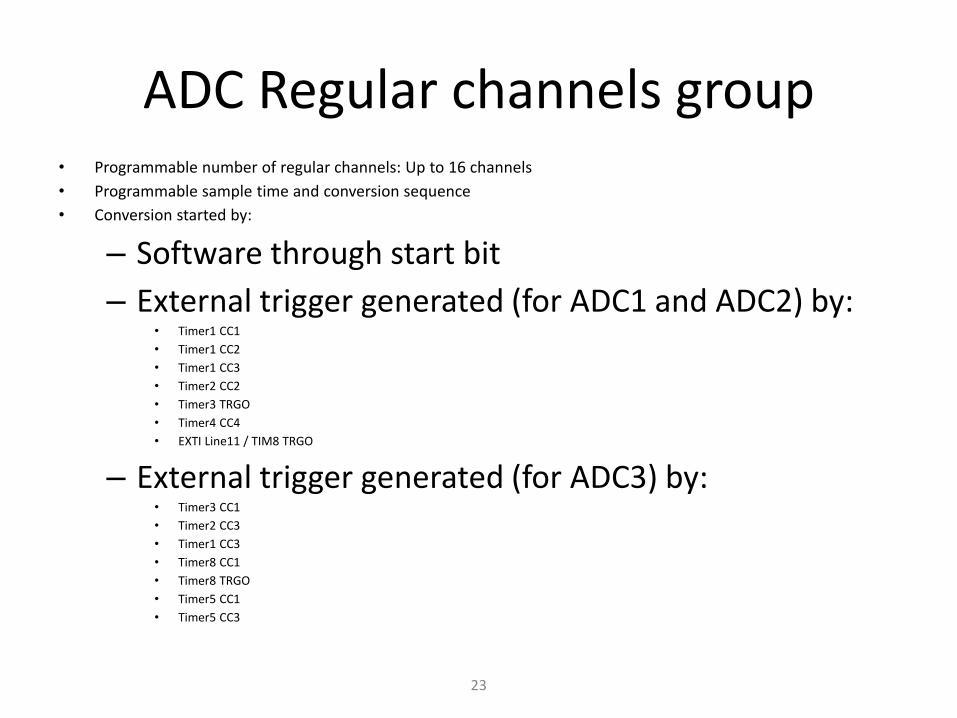
ADC Regular channels group • Programmable number of regular channels: Up to 16 channels
• Programmable sample time and conversion sequence
• Conversion started by:
– Software through start bit
– External trigger generated (for ADC1 and ADC2) by: • Timer1 CC1
• Timer1 CC2
• Timer1 CC3
• Timer2 CC2
• Timer3 TRGO
• Timer4 CC4
• EXTI Line11 / TIM8 TRGO
– External trigger generated (for ADC3) by: • Timer3 CC1
• Timer2 CC3
• Timer1 CC3
• Timer8 CC1
• Timer8 TRGO
• Timer5 CC1
• Timer5 CC3

24
ADC Injected channels group • Programmable number of injected channels: Up to 4 channels
• Programmable sample time and conversion sequence
• Conversion started by: – JAUTO: automatic injected conversion after regular channels
conversion
– Software through start bit
– External trigger generated (for ADC1 and ADC2) by: • Timer1 TRGO
• Timer1 CC4
• Timer2 TRGO
• Timer2 CC1
• Timer3 CC4
• Timer4 TRGO
• EXTI Line15 / TIM8 CC4
– External trigger generated (for ADC3) by: • Timer1 TRGO
• Timer1 CC4
• Timer4 CC3
• Timer8 CC2
• Timer8 CC4
• Timer5 TRGO
• Timer5 CC4

25
Advanced Control, General Purpose and Basic Timers

26
8 Timers w/ advanced control features
• Two Advanced Control Timers: TIM1 and TIM8
• Four General Purpose Timers: TIM2, TIM3, TIM4 and TIM5
• Two Basic Timers: TIM6 and TIM7

27
Basic Timers Features Overview
• TIM6, 7 on Low Speed APB (APB1)
• Internal clock up to 72 MHz
• 16-bit auto-reload up-counter
• Interrupt/DMA generation on the update event
• Synchronization circuit to trigger the DAC
Can be used as generic timers for time-base generation but they are also specifically used to drive the Digital-to-Analog Converter (DAC)
16-Bit Prescaler
Trigger/Clock
Controller
Trigger Output
to DAC
TIMxCLK
Auto Reload REG
+/- 16-Bit Counter
Update event
IT & DMA

NVIC - Nested Vector Interrupt Controller
The Nested Vector Interrupt Controller is a standard unit within the Cortex core. This means that all Cortex-based microcontrollers will have the same interrupt structure, regardless of manufacturer.

NVIC
The NVIC will respond to an interrupt with a latency of twelve cycles. This includes a microcoded routine to automatically push a set of registers onto the stack.

Tail-chaining
Multiple interrupts will be ‘tail chained’ so there is a minimum delay of six cycles from the end of one interrupt to the start of the next.

Interrupt response - Example Highest
IRQ1
IRQ2
ISR 2 Starts
NMI
IRQ3
Push for ISR1 begins
Pre-empted by NMI
New instruction fetch in
parallel minimises time to NMI
NMI ISR 1 ISR 2 ISR 3 POP PUSH PUSH
Cortex-M3 •Following NMI processor tail-chains into ISR1 •ISR2 Completed •Pop only occurs on return to “Main”
POP

Exception Vector Types and Priority
The Cortex exception table contains the start address or an ISR which is loaded into the Program counter as the CPU enters the exception.

Vector Table
33
• Vector Table starts at location 0
– In the code section of the memory map
• Vector Table contains addresses (vectors)
of exception handlers and ISRs
– Not instructions like other ARM processors
• Table size (in words) is = number of IRQ inputs + 16
– Minimum size ( case of 1 IRQ) : 17 words
– Maximum size ( case of 240 IRQs) 256 words
• Main stack pointer initial value in location 0
– Set up by hardware during Reset
• Vector Table can be relocated (to SRAM)
– Software configurable through dedicated register in SCB
Address Vector
0x00 Initial Main SP
0x04 Reset
0x08 NMI
0x0C Hard Fault
0x10 Memory Manage
0x14 Bus Fault
0x18 Usage Fault
0x1C-0x28 Reserved
0x2C SVCall
0x30 Debug Monitor
0x34 Reserved
0x38 PendSV
0x3C Systick
40 IRQ0
… More IRQs
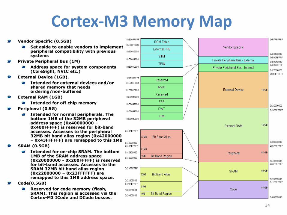
Cortex-M3 Memory Map
34
Vendor Specific (0.5GB)
Set aside to enable vendors to implement peripheral compatibility with previous systems
Private Peripheral Bus (1M)
Address space for system components (CoreSight, NVIC etc.)
External Device (1GB).
Intended for external devices and/or shared memory that needs ordering/non-buffered
External RAM (1GB)
Intended for off chip memory
Peripheral (0.5G)
Intended for normal peripherals. The bottom 1MB of the 32MB peripheral address space (0x40000000 – 0x400FFFFF) is reserved for bit-band accesses. Accesses to the peripheral 32MB bit band alias region (0x42000000 – 0x43FFFFFF) are remapped to this 1MB
SRAM (0.5GB)
Intended for on-chip SRAM. The bottom 1MB of the SRAM address space (0x20000000 - 0x200FFFFF) is reserved for bit-band accesses. Accesses to the SRAM 32MB bit band alias region (0x22000000 – 0x23FFFFFF) are remapped to this 1MB address space.
Code(0.5GB)
Reserved for code memory (flash, SRAM). This region is accessed via the Cortex-M3 ICode and DCode busses.

Interrupt enable bits
Each interrupt source has an enable bit in the NVIC and in the peripheral. In the STM32 there are sixteen levels of priority.

NVIC Configuration And Use
To use the NVIC we need to do three things. 1. Configure the vector table for the
interrupt sources we want to use 2. Configure the NVIC registers to enable
and set the priorities of the NVIC interrupts
3. Configure the peripheral and enable its interrupt support.

Power supply
The STM32 runs from a single 2.0V-3.6V supply. There is an additional backup power domain and a separate supply for the ADC converter (144 pin package only).

Supply stabilisation capacitors
With an internal reset and an internal voltage regulator, the STM32 only needs seven external capacitors.

Basic Hardware Schematic

Clock Schemes
40
2 external clocks 2 internal clocks 1 PLL

Internal Oscillator
The STM32 has internal RC oscillators which are capable of supplying a clock to the internal PLL. This will allow the microcontroller to run at its maximum 72 MHz clock frequency. The internal oscillators are not as accurate or stable as an external crystal; consequently for most designs you will need at least one clock source.

External Oscillator
The External Oscillator can be run from a crystal or external clock source.

Boot Modes
The external boot pins are used to select which region of memory aliased to the first 2k of memory. This can be user Flash, the internal bootloader or the first 2k of SRAM

Superloop system (single task system)
• Tasks executes in sequence • No realtime OS, real time not important • Using interrupt for time critical tasks • Hard to use in big systems
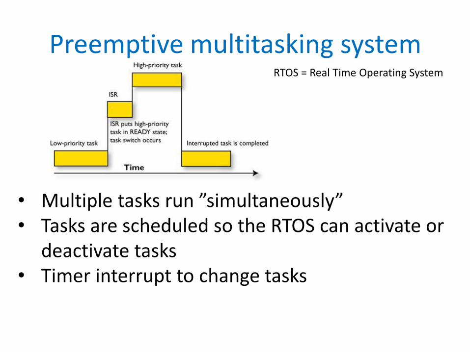
Preemptive multitasking system
• Multiple tasks run ”simultaneously” • Tasks are scheduled so the RTOS can activate or
deactivate tasks • Timer interrupt to change tasks
RTOS = Real Time Operating System