frequency control and stabilization of a laser system
TRANSCRIPT

Frequency Control and Stabilization of a LaserSystem
Chu Cheyenne Teng
Advisor: Professor David A. HannekeDecember 10, 2013
Submitted to theDepartment of Physics of Amherst College
in partial fulfilment of therequirements for the degree ofBachelors of Arts with honors
c© 2013 Chu Cheyenne Teng
Abstract
Quantum logic spectroscopy enables state manipulation and precise spectral mea-surement of many charged atoms and molecules. One application of this techniqueis precise spectroscopy of molecules, which can improve searches for the time varia-tion of the proton-electron mass ratio (µ). By co-trapping the molecular ion with anatomic ion, the two ions are coupled through the Coulomb interactions. Because ofthis, the cooling and internal state preparation of an atomic ion, in our case 9Be+,are extended to the molecular ion.
My thesis describes the construction of a stable and versatile laser system forefficient cooling, state preparation, and detection of 9Be+. We demonstrate a laserlock that transfers the frequency stability of a helium-neon laser to less stable lasersusing a Fabry-Perot cavity. An external frequency reference, provided by a thalliumfluoride molecular transition, shows that the system is stable to within 200 kHz over3 hours. We also performed injection current modulation on an external cavity diodelaser in order to produce a frequency detuning critical for the cooling scheme. Thecurrent setup can achieve a maximum modulation frequency of 6.6 GHz with 3 % ofthe output power in an optical sideband.

Acknowledgments
Professor Hanneke, thank you. In the past two years, you have been a most resourceful
and passionate mentor to me. The weekly meetings that were once intimidating, and
at times confusing, have actually turned into something I enjoy and look forward
to–it’s true!
Thank you, my physics professors. You have always been available and supportive.
A major part of my Amherst experience consists of you, and I am thankful and happy
for that.
A special thanks to the Friedman Lab, for generously lending me the rf generator.
It is critical for half of my thesis. Thank you Steve Peck, for your company in lab over
the summer and your powerful Labview skill. And Jim Kubasek, my thesis would
not have been possible without you.
To my labmates and my friends, I have said little in the past, but I feel so lucky
to have known you and spent time with you.
I am grateful for the generous support from the Amherst College Dean of the
Faculty, National Science Foundation, and the Research Corporation for Science Ad-
vancement.
Last but not least, I am most fortunate to have my sweet family. Mom, Dad, and
Cavell, thank you for your patience, support, and love.
i

Contents
1 Introduction 11.1 Why Beryllium Ion? . . . . . . . . . . . . . . . . . . . . . . . . . . . 31.2 Internal State Preparation and Detection . . . . . . . . . . . . . . . . 41.3 Doppler Cooling . . . . . . . . . . . . . . . . . . . . . . . . . . . . . . 61.4 Resolved Sideband Cooling . . . . . . . . . . . . . . . . . . . . . . . . 7
1.4.1 Stimulated Raman Transitions . . . . . . . . . . . . . . . . . . 71.4.2 Laser Repumping . . . . . . . . . . . . . . . . . . . . . . . . . 9
1.5 An Overview . . . . . . . . . . . . . . . . . . . . . . . . . . . . . . . 10
2 Frequency Stabilization: The Scanning Fabry-Perot Cavity 122.1 System Setup . . . . . . . . . . . . . . . . . . . . . . . . . . . . . . . 132.2 The Confocal Fabry-Perot Cavity . . . . . . . . . . . . . . . . . . . . 15
2.2.1 The Basic Theory . . . . . . . . . . . . . . . . . . . . . . . . . 162.2.2 Athermal Cavity Design . . . . . . . . . . . . . . . . . . . . . 202.2.3 Obtaining the Confocal Condition . . . . . . . . . . . . . . . . 25
2.3 The External Cavity Diode Laser . . . . . . . . . . . . . . . . . . . . 272.3.1 The Diffraction Grating . . . . . . . . . . . . . . . . . . . . . 30
2.4 System Performance . . . . . . . . . . . . . . . . . . . . . . . . . . . 322.4.1 System Stability . . . . . . . . . . . . . . . . . . . . . . . . . 322.4.2 Reaction to Temperature Drifts . . . . . . . . . . . . . . . . . 362.4.3 The Other Factors . . . . . . . . . . . . . . . . . . . . . . . . 38
3 Injection Current Modulation 403.1 Experimental Setup . . . . . . . . . . . . . . . . . . . . . . . . . . . . 413.2 Supporting Theory . . . . . . . . . . . . . . . . . . . . . . . . . . . . 42
3.2.1 p− n Junctions . . . . . . . . . . . . . . . . . . . . . . . . . . 423.2.2 Radiative and Non-radiative Mechanisms . . . . . . . . . . . . 443.2.3 The Rate Equations . . . . . . . . . . . . . . . . . . . . . . . 453.2.4 The AM Theory . . . . . . . . . . . . . . . . . . . . . . . . . 493.2.5 The FM Theory . . . . . . . . . . . . . . . . . . . . . . . . . . 50
ii
3.2.6 Optical Sidebands . . . . . . . . . . . . . . . . . . . . . . . . . 513.3 Experimental Observations . . . . . . . . . . . . . . . . . . . . . . . . 54
3.3.1 General Decline with Increasing Modulation Frequency . . . . 573.3.2 Dramatic Improvements from External Cavity Feedback . . . 603.3.3 Bias Current Dependence . . . . . . . . . . . . . . . . . . . . 613.3.4 Frequency of Oscillation Relaxations . . . . . . . . . . . . . . 633.3.5 Mysterious Sidebands . . . . . . . . . . . . . . . . . . . . . . . 65
4 Conclusion 68
A Optical Sideband Derivations 70
B Allan Deviation 73
iii
List of Figures
1.1 Energy Level Diagram for 9Be+ . . . . . . . . . . . . . . . . . . . . . 41.2 Stimulated Raman Transitions . . . . . . . . . . . . . . . . . . . . . . 81.3 Required Lasers . . . . . . . . . . . . . . . . . . . . . . . . . . . . . . 11
2.1 F-P System Setup . . . . . . . . . . . . . . . . . . . . . . . . . . . . . 132.2 DAQ Analog I/O . . . . . . . . . . . . . . . . . . . . . . . . . . . . . 152.3 F-P Cavity Beam Path . . . . . . . . . . . . . . . . . . . . . . . . . . 162.4 Cartoon of The F-P Cavity . . . . . . . . . . . . . . . . . . . . . . . 202.5 Demonstration of the Radius of Curvature . . . . . . . . . . . . . . . 232.6 Cartoon of The F-P Cavity . . . . . . . . . . . . . . . . . . . . . . . 232.7 F-P System Photos . . . . . . . . . . . . . . . . . . . . . . . . . . . . 242.8 Photo of Complete Setup . . . . . . . . . . . . . . . . . . . . . . . . . 252.9 Single HeNe Transmission Peak . . . . . . . . . . . . . . . . . . . . . 262.10 Multiple HeNe Transmission Peaks . . . . . . . . . . . . . . . . . . . 282.11 ECDL photo . . . . . . . . . . . . . . . . . . . . . . . . . . . . . . . . 292.12 Diffraction Grating Illustration . . . . . . . . . . . . . . . . . . . . . 302.13 TlF Transition Peak . . . . . . . . . . . . . . . . . . . . . . . . . . . 332.14 System Stability Over 3 Hours . . . . . . . . . . . . . . . . . . . . . . 342.15 Laser Frequency Unlocked . . . . . . . . . . . . . . . . . . . . . . . . 352.16 Allan Deviation Plot . . . . . . . . . . . . . . . . . . . . . . . . . . . 362.17 Frequency vs. Temperature . . . . . . . . . . . . . . . . . . . . . . . 372.18 Laser Power Drift . . . . . . . . . . . . . . . . . . . . . . . . . . . . . 382.19 Channel A/Channel B . . . . . . . . . . . . . . . . . . . . . . . . . . 39
3.1 Injection Current Modulation Setup . . . . . . . . . . . . . . . . . . . 413.2 p− n Junction . . . . . . . . . . . . . . . . . . . . . . . . . . . . . . 433.3 Stimulated Emission . . . . . . . . . . . . . . . . . . . . . . . . . . . 443.4 Bessel Functions . . . . . . . . . . . . . . . . . . . . . . . . . . . . . 533.5 Sideband Patterns . . . . . . . . . . . . . . . . . . . . . . . . . . . . 553.6 Coincident First Sidebands . . . . . . . . . . . . . . . . . . . . . . . . 563.7 Sideband Illustration . . . . . . . . . . . . . . . . . . . . . . . . . . . 57
iv
3.8 Reflected RF Power . . . . . . . . . . . . . . . . . . . . . . . . . . . . 583.9 Modulation Depth . . . . . . . . . . . . . . . . . . . . . . . . . . . . 593.10 Modulation Indices . . . . . . . . . . . . . . . . . . . . . . . . . . . . 603.11 Bias Current Dependence at 4300 MHz (Modulation Depth) . . . . . 623.12 Bias Current Dependence at 4300 MHz (Modulation Indices) . . . . . 633.13 Bias Current Dependence at 6644 MHz (Modulation Indices) . . . . . 643.14 Bias Current Dependence at 6644 MHz (Modulation Depth) . . . . . 643.15 Unexpected Sidebands . . . . . . . . . . . . . . . . . . . . . . . . . . 66
v

Chapter 1
Introduction
We plan to build a system capable of performing spectroscopy on a variety of charged
species. Such a system will be a versatile tool for studying species whose more com-
plicated structures previously hindered precise spectral measurements. A useful ap-
plication of this system is to measure the time variation of the proton-electron mass
ratio (µ) using molecules. Since several physical theories seeking to unify general
relativity with quantum mechanics predict that µ changes over time, more sensitive
measurements of dµ/dt, which this setup can potentially offer, can serve to confirm
or disprove these theories.[1]
In contrast to atoms, molecules lack the structural simplicity that allows for effec-
tive cooling and internal state preparation. This is why despite having energy tran-
sitions that are more sensitive to variations in µ than atoms, molecular spectroscopy
has not been a popular choice for measuring dµ/dt. Our goal is to take advantage of
the more sensitive spectroscopy transitions in molecules while exploiting the favorable
features of the atoms using quantum logic spectroscopy.
1

We realize quantum logic spectroscopy in three steps. First, we co-trap a diatomic
molecular ion (designated the spectroscopy ion) with an atomic ion (designated the
logic ion) in a linear Paul trap designed by Shenglan Qiao.[2] Second, the spectroscopy
ion is sympathetically cooled to its translational ground state because of the motional
coupling between the two ions through Coulomb interactions.1 The spectroscopy ion
is then further cooled to its rotational ground state without disturbing its translational
and vibrational states. Third, we manipulate the internal states of the spectroscopy
ion in order to measure the desired transition frequency. We are currently constructing
the apparatus for the first two steps.
My thesis focuses on the second step, where a stable laser system is required for
sympathetic cooling and state initialization. In this thesis, I demonstrate a frequency
lock that stabilizes the frequency of the lasing source, which is an external cavity
diode laser (ECDL). I also show that injection current modulation of the ECDL is
a convenient and viable method that allows us to obtain all of the required laser
frequencies from the ECDL.2
For the rest of this chapter, I first discuss the reasons behind our choice of the logic
ion, 9Be+, in Sec. 1.1. Then I provide some details about the cooling methods that
we plan to use–Doppler cooling and resolved sideband cooling. The implementation
of the cooling scheme will directly motivate the rest of this thesis.
1In room temperature, the molecules are mostly in their vibrational ground states.2The ECDL provides a laser beam at 940nm, which is converted into 313nm using the setup
designed by Celia Ou.[3] Note that frequency conversion happens after injection current modulationand both the original ECDL output and the modulated output are frequency converted with thefrequency difference between them preserved.
2

1.1 Why Beryllium Ion?
Since quantum logic spectroscopy relies on the Coulomb interaction between the logic
ion and the spectroscopy ion, 9Be+ satisfies the very first criterion: being an ion. With
a single valence electron, 9Be+ also has a simple and well-studied structure that makes
it a popular choice for atomic trapping and cooling. It is also important that 9Be+
has a nuclear spin I = 3/2. When subject to a magnetic field, the nuclear spin
couples with the valence electron spin (S = 1/2) to form hyperfine structures. For
effective atomic state manipulations, hyperfine structures are preferable because of
their relatively large spectral splittings (1.25 GHz for the two hyperfine states we are
interested in) and long decay times (∼ 1015s). [4, p 13]
Fig. 1.1 shows the energy level diagram of a 9Be+. The ground state has a total
of 8 hyperfine states, which I show split under the influence of a magnetic field.3
The first excited states of 9Be+ consist of the fine structure manifold due to spin-
orbit coupling. Each of the resulting P1/2 and P3/2 states also has its own hyperfine
structures: P1/2 contains 8 hyperfine states and P3/2 contains 16 hyperfine states.
Note that the fine structure splitting between the two excited P states is 197 GHz.
This large splitting allows us to safely ignore the P1/2 states when we excite the atoms
to the P3/2 states.
We have designated S1/2|F = 2,mF = 2〉 to be |↓〉 and S1/2|1, 1〉 as |↑ 〉, and the
energy splitting between them corresponds to ∼1.25 GHz. The reason for this labeling
will become obvious when we discuss stimulated Raman transitions in Sec. 1.4.
3For I = 3/2 and S = 1/2, F can be either 1 or 2, and for each F we can have 2F + 1 hyperfinestates corresponding to each allowed mF .
3

|F = 2,mF = −2〉|2,−1〉
|2, 0〉|2, 1〉
|2, 2〉 = |↓〉
|1, 1〉 = |↑〉|1, 0〉
|1,−1〉
S1/2
|mF = −2〉 to |mF = 2〉P1/2
|mF = −3〉 to |mF = 3〉P3/2
197 GHz
∆(6.6 GHz)
313.132nm957.396 THz
fhfs
(∼1.25 GHz)
Figure 1.1: The energy level diagram for 9Be+. The S1/2 hyperfine manifold is illus-trated. P3/2 contains 16 hyperfine levels and the P1/2 contains 8 hyperfine levels. Thedashed line shows a detuning of 6.6 GHz from P3/2, which will be used for Ramantransitions.
1.2 Internal State Preparation and Detection
In order to reliably detect the internal state of the logic ions, we use a cycling tran-
sition that allows us to continuously observe scattered photons without disturbing
the prepared atomic states. We choose the cycling transition between S1/2|2, 2〉 and
4

P3/2|3, 3〉. Once excited to the P3/2|3, 3〉 state, the atoms can only decay back to
S1/2|2, 2〉 because the selection rule requires ∆mF = ±1 or 0, and there are no ground
states with mF = 3 or 4. Under a detection beam that is resonant with this cycling
transition, the atoms are restricted to cycle only between these two states, leading to
continuous spontaneous emissions.
It is important to make sure that the detection beam stays resonant with the cy-
cling transition for accurate detection. Note that the linewidth of the P3/2|3, 3〉 state
is only 19.4 MHz. If the laser frequency drifts beyond this range, we no longer detect
photons firstly because the laser is no longer resonant with the cycling transition,
and secondly because it cannot drive any other atomic transitions due to its polariza-
tion. This is the principal reason for stabilizing our laser frequencies; the frequency
stabilization scheme is discussed in Chapter 2.
To enable the cycling transition, we need to initiate 9Be+ in the S1/2|2, 2〉 state.
Note that the atoms are distributed among the ground-state hyperfine manifold be-
cause excited states decay quickly. The Doppler beams that we will discuss in the
following section address atoms in all of the ground states because they are detuned
within the linewidth of the ground state. For now, we use the Doppler beams for
optical pumping. Since the S1/2|2, 2〉 state has the highest mF among all of the hy-
perfine states in S1/2, we use right circularly polarized (σ+) Doppler beams because
the selection rule requires that ∆mF = +1 for each excitation. Again by the selection
rule, the excited atom can either decay to a state with the same mF or a higher mF
in comparison to the original state before excitation. Eventually all of the atoms end
up in S1/2|2, 2〉, where they become resonant with the cycling transition.
5

1.3 Doppler Cooling
The Doppler beams mentioned in the previous section are named for their roles in
Doppler cooling. Since quantum logic spectroscopy couples the motions of the spec-
troscopy ion and the logic ion, it is crucial to reduce the translational motion of the
logic ions to a known ground state for efficient state manipulations.
In Doppler cooling, the laser is tuned to the red of the resonant frequency. In the
frame of reference of an atom moving towards a laser beam, the laser appears blue-
shifted due to Doppler shift. When the red-detuning of the laser matches with the
amount of blue-shift that the atom perceives, the laser beam becomes resonant with
the atom. The atom thus first absorbs a photon, then emits one due to spontaneous
emission. While the absorbed photon has a definite momentum against the direction
of the atom, the emitted photon has an average momentum of 0 due to the random
direction of emission. The net momentum imparted on the atom causes the atom to
lose kinetic energy, hence lowering its temperature.
In our experiment, we first use a Doppler beam detuned by a few hundred MHz
to address atoms with a wide range of velocities. This prepares the atoms for finer
coolings from a second, less detuned Doppler beam (by half the linewidth of the
excited state) to complete Doppler cooling. While free-space experiments require
three pairs of cooling beams to cool atoms traveling in all directions, our atoms are
already confined to a harmonic potential well4. Because of this, a single Doppler beam
can cool all three atomic motions provided some of the laser’s propagation direction
lies along each trap axis.
4Both the spectroscopy ions and the logic ions will be housed in a linear Paul trap. The potentialwithin the trap is analogous to a harmonic well.
6
Note that although Doppler cooling is an efficient cooling method, it cannot lower
the temperature of the atoms beyond the Doppler limit. This limit is due to the
background heating from the very process of absorption and emission that enabled
Doppler Cooling. To further cool the atoms to sub-Doppler temperatures, we need
to use a second cooling method called resolved sideband cooling.
1.4 Resolved Sideband Cooling
In order to cool the atoms beyond the Doppler limit, we consider their quantized
vibrational motions (labled |n〉) due to the harmonic potential of the trap. Sub-
Doppler cooling involves reducing the atoms to the lowest vibrational levels (|n = 0〉).
We plan to achieve this in two steps. First we use stimulated Raman transitions to
couple | ↓, n〉 with | ↑, n − 1〉. We then repump the atoms to | ↓〉 without exciting
their vibrational motions. The goal is to repeat this process enough times to cool the
atoms to |↓, 0〉.
1.4.1 Stimulated Raman Transitions
The first step in resolved sideband cooling is to couple the vibrational states of | ↓〉
and | ↑〉 using stimulated Raman transitions. As Fig. 1.2 shows, the setup requires
two laser beams that indirectly couple |↓, n〉 and |↑, n− 1〉 through a third, transient
excited state far detuned from the actual excited state.
In stimulated Raman transitions, the atom absorbs a photon corresponding to the
energy of one of the laser beams, then emits one with the same energy as the other
laser beam. While spontaneous emission produces photons with exactly the energy
7

P3/2
|↑, n− 1〉
|↓, n〉
∆=6.6 GHz
fr
fb
Rabi flopping
fhfs
1.25 GHz
n = 0n = 1n = 2
|↑〉
n = 0n = 1n = 2
|↓〉
fn
Rabi flopping
Figure 1.2: Left: Stimulated Raman transitions between | ↑〉 and | ↓〉 through atransient excited state detuned by 6.6 GHz from the actual excited state. Two laserbeams are required for this operation: the Red Raman beam with frequency fr andthe Blue Raman beam with frequency fb. Right: The first three vibrational states of|↑〉 and |↓〉. The Raman transitions result in the coherent coupling between |↑, n−1〉and | ↓, n〉. Note that adjacent vibrational states differ by fn in angular frequency.Both figure are not drawn to scale.
difference between the excited state and the ground state, stimulated emissions in
Raman transitions allow control of the energy and direction of the emitted photon.
Since the linewidth of a P3/2 hyperfine state is 19.4 MHz, a large detuning such
as 6.6 GHz significantly suppresses spontaneous emissions, effectively reducing the
transition to only between the two states of interest.
In order to couple |↓, n〉 and |↑, n−1〉, the frequency difference of the two Raman
beams has to correspond to the energy difference between these two states. Given
the hyperfine splitting between these two states (fhfs), which can be controlled by
adjusting the strength of the magnetic field, and the frequency difference between
two adjacent vibrational states (fn), the required frequency difference between the
two lasers should be fhfs−fn. These two laser beams cause the population distribution
8

of 9Be+ to oscillate between |↓, n〉 and |↑, n− 1〉 with a frequency known as the Rabi
frequency. A similar phenomenon is observed in nuclear magnetic resonance, where
an oscillating magnetic field causes the nuclear magnetic moment to oscillate between
two spin states.
With π-pulses, Rabi flopping leaves the atoms in the | ↑〉 state. We need a way
to switch the atoms back to | ↓〉 while preserving its lower vibrational state, and a
repump laser is used for this purpose.
1.4.2 Laser Repumping
To transfer | ↑, n − 1〉 to | ↓, n − 1〉, we use a σ+ polarized laser beam to excite the
atoms to a state in P3/2 with mF = 2. Due to the large hyperfine splitting (1.25
GHz) in the ground state, this laser is resonant with | ↑〉 while largely detuned from
| ↓〉. From the excited states, angular momentum selection rules allow the atoms to
decay to one of the three ground states: |2, 2〉, |2, 1〉, or |1, 1〉.5 In the first case, we
have successfully arrived at | ↓, n − 1〉. In the second case, we apply an rf drive at
a frequency of fhfs to pump the atoms back to | ↑〉. The atoms from the last case,
along with those pumped by the rf drive to | ↑〉, will be resonant with the repump
laser beam again. Through repeated Raman transitions and repumping, all of the
atoms are eventually transferred to |↓, 0〉, where they are no longer coupled with |↑〉
because there is no |n = −1〉 vibrational level.
5The selection rule is ∆mF = ±1, 0, but there is no |2, 3〉 or |1, 3〉 states.
9

1.5 An Overview
We have introduced all of the required laser beams for state initialization, detection,
and cooling of the logic ion. Fig 1.3 lists all six required laser beams with specific
frequencies and polarizations attached. Through injection current modulation of
the external cavity diode laser (ECDL), we obtain an optical sideband detuned by
∆ (∼ 6.6 GHz) from the carrier frequency (fL).6 The detection, cooling, detuned
cooling, and repump beams can be obtained from modulating the optical sideband
using acousto-optic modulators (AOMs). The carrier is also modulated by AOMs to
generate the Red Raman and the Blue Raman beams. Note that with δ at around 600
MHz, the detuned cooling beam can address all of the hyperfine levels in the ground
state. The polarization choices of the first four σ+ polarized lasers listed in the figure
are required for angular momentum conservation, as discussed earlier in this chapter.
Because non-resonant laser fields cause Stark shifts in |↓〉 and |↑〉, both Red Raman
and Blue Raman beams contain σ+ and σ− in order to minimize the energy shift.[5]
In addition, the Blue Raman has π polarized light so that along with the σ− light in
Blue Raman, we obtain the desired Raman transitions.
My thesis helps to build such a laser system as specified in Fig. 1.3. In Chapter
2, I present a laser locking system that I built to stabilize the frequencies of these
lasers. In Chapter 3, I provide the details of using injection current modulation to
produce the detuning (∆) from the excited states.
6The figure shows ∆ ∼9 GHz, that was our original plan. As we discovered in Chapter 3, ourECDL can only be modulated up to 6.6 GHz. This detuning should still be large enough.
10

f L
∆ (e
.g. 9
GH
z)
δ (e
.g. 6
00 M
Hz)
f hfs (1
.25
GH
z)
Line
wid
th 1
9.4
MH
zP 3/
2
S 1/2|1
,1⟩
|2,2
⟩
Det
ectio
n:
f L +
∆ +
δ
σ+
Cool
ing:
f L +
∆ +
δ -
10 M
Hz
σ+
Det
uned
coo
ling:
f L + ∆
+ δ
- fe
w 1
00 M
Hz
σ+
Repu
mp
(with
rf a
ssis
t):
f L + ∆
+ δ
- f hf
s
σ+
Red
Ram
an:
f L +
δ -
f hfs +
/- 1
0 M
Hz
π,
σ+ , σ
−
Blue
Ram
an:
f L +
δ +
/- 1
0 M
Hz
σ+ /σ−
Ram
an δ
can
be
di�e
rent
from
reso
nant
δ.
Onl
y on
e Ra
man
bea
m n
eeds
to b
e +/
- 10
MH
z.
9 Be+ P
3/2 -
S 1/2
313.
132
922
nm, 3
1 93
5.31
9 8
cm-1
, 957
.396
802
TH
z(d
iv. b
y 3)
939
.398
766
nm
, 10
645.
106
6 cm
-1, 3
19.1
32 2
67 T
Hz
9 Be+ P
1/2 -
S 1/2
313.
197
416
nm, 3
1 92
8.74
3 6
cm-1
, 957
199
652
TH
z
Figure 1.3: The laser beams needed for cooling and state initialization of 9Be+. fLrefers to the carrier frequency of the external cavity diode laser; δ and the specifiedfrequencies detunings in MHz are realized using the acousto-optic modulators and ∆results from injection current modulation. Figure courtesy of Professor Hanneke.
11

Chapter 2
Frequency Stabilization: The
Scanning Fabry-Perot Cavity
A stable lasing source is integral to an effective quantum logic spectroscopy setup.
More specifically, efficient state preparation and cooling of the logic ion, 9Be+, requires
that our lasers are stable enough for the linewidth of a P3/2 excited state, which is
19.4 MHz (refer to Chapter 1 for detail).
In this chapter, we present a laser locking system that uses a confocal Fabry-Perot
cavity to transfer the frequency stability of a helium-neon laser to our tunable lasing
source, the external cavity diode laser (ECDL). The F-P cavity detects laser frequency
drifts by comparing the wavelengths between the ECDL and the HeNe laser using a
common length reference between two spherical mirrors. In order to obtain sensitive
detection, which is critical for effective frequency stabilization, the common length
reference must be kept stable. This concern guides the construction of the cavity as
we took measures to stabilize the temperature and pressure within the cavity.
12
2.1 System Setup
A laser becomes resonant with the Fabry-Perot (F-P) cavity when an integer multi-
ple of the laser’s wavelength fits into its beam path within the cavity. At resonant
conditions, we observe transmission peaks at the outputs of the F-P cavity. As we
continuously scan the cavity length at a constant speed, a stable laser registers trans-
mission peaks at equal time intervals. When the frequency drifts, this time interval
varies. This allows a scanning F-P cavity to translate frequency drifts into transmis-
sion peak drifts when observed on an oscilloscope.
F-P Cavity
HeNe
ECDLPD1PD2
Dichroicbeamsplitter
Dichroicbeamsplitter
mirror
Figure 2.1: F-P cavity setup. The HeNe and IR beams are combined to a dichroicbeamsplitter, where the HeNe beam is reflected and the IR is transmitted. Thecombined beam passes through the F-P cavity, until another dichroic beamsplittersplits them up on the other end of the cavity. Each beam is then detected by aphotodetector. Note that some auxiliary mirrors used in practice to help direct beamsare omitted in this figure.
We use a helium-neon laser (HeNe)1 as a stable frequency reference. By measuring
1We use an ultra stable Melles Griot HeNe (Part number 05-STP-901). Its stability in frequency-
13

the change in the time interval between an ECDL transmission peak and a HeNe
transmission peak, we generate an error signal proportional to the laser frequency
drift.
As shown in Fig. 2.1, the HeNe and the IR beam from the ECDL are combined
onto the same beam path using a dichroic beamsplitter (Semrock FF678-Di01); the
HeNe is reflected while the IR is transmitted. The converging lenses on both sides
of the cavity enhance output signal by counteracting the diverging effects of the end
mirrors.2 At the output of the F-P cavity, the HeNe beam is separated from the IR
using another dichroic beamsplitter.3 The transmission peaks of individual lasers are
independently detected by photodectors.
Fig. 2.2 illustrates how we implement the laser lock. As shown, the locking scheme
is facilitated by a data acquisition device (NI DAQ, part number USB-6343), which is
controlled by a Labview program.4 We obtain a triangle wave signal from the DAQ,
which is amplified by a piezo driver before sending to the piezo in the F-P cavity. The
cavity length is scanned as this piezo (Noliac NAC2123-A01) expands or contracts
depending on the supplied voltage. The resulting transmission signals are detected
by photodetectors and sent to the computer through the DAQ. By detecting changes
in the spacing between a HeNe transmission peak and an IR transmission peak,
the Labview program calculates a corresponding correction based on a proportional-
integral-derivative (PID) algorithm. Since the ECDL frequency can be tuned by
stabilized mode is specified at 3 MHz over 8 hours.2Our end mirrors are plano-concave, as demonstrated in Fig. 2.1. Without the converging lens,
laser light incident on an end mirror will diverge within the cavity, causing the beam path to straytoo far from the central axis and resulting in poor output signal.
3We divide one Semrock beamsplitter into two independent beamsplitters.4The program is titled JeffLock; it is inherited from the DeMille lab at Yale. It is the only
Labview program needed to automatically lock the laser frequency to the HeNe.
14

tilting the diffraction grating (see Sec 2.3.1 for detail), the DAQ sends a correction
voltage to another piezo driver, which controls the piezo behind the diffraction grating
to correct for frequency drifts.
OUT OUT IN IN
Piezo Driver 2
PD1-HeNe
PD2-IR
DAQ (NI USB-6343)
F-P Cavity
HeNeMelles Griot 05-STP-901
Piezo Driver 1
ECDLdiffraction
grating
Computer
IR
HeNe
Figure 2.2: An illustration of the analog inputs and outputs of the data acquisitiondevice (DAQ). The DAQ controls the piezos in the F-P cavity in the ECDL. It alsoreads HeNe and IR outputs from the photodetectors.
2.2 The Confocal Fabry-Perot Cavity
In the previous section, we see the central role of the Fabry-Perot (F-P) cavity in our
locking scheme. We now introduce the confocal model that we adopted in our lab
and describe its properties.
15

2.2.1 The Basic Theory
An F-P cavity consists of two end mirrors whose highly reflective surfaces face each
other. A beam of light entering the cavity will make multiple passes between the
mirrors. When these beams interfere constructively, the intensity of light builds up
dramatically. Under this resonant condition, the high laser intensity within the cavity
leads to transmission despite low transmittance of the end mirrors.5
In a confocal F-P cavity, the foci of two concave spherical mirrors coincide at the
center of the cavity. This requires that the two end mirrors have equal radius of
curvature(R) and that their separating distance(L) is equal to R. As will be seen, the
confocal design is convenient because its behavior is largely insensitive to the shape
and position of the input beam.
L = R
Incident Beam
Front Output 1
Front Output 2
Rear Output 1
Rear Output 2
focus
Figure 2.3: The beam path of a parallel beam incident on the F-P cavity. Arrowsindicate propagation directions. The focal point is located at the center of the cavity,where the beam paths intersect. The distance between the mirrors corresponds tothe radius of curvature (R). This figure is not drawn to scale.
In Fig. 2.3, the incident beam travels a distance close to 4L within the cavity
before retracing its path. At resonance, there are two output beams at each side of
5High reflectivity of the end mirrors necessarily corresponds to low transmittance. Since theresonant effect is more important, higher reflectivity is usually better.
16

the cavity. While the front outputs diverge, the rear outputs propagate in the same
direction as the incident beam. In principle all four outputs observe transmission
peaks. In practice we choose one of the rear outputs as our signal because of the
relatively small beam size.
Note that the incident beam does not have to be propagating along the central axis
of the cavity. Any incident beam parallel to the central axis will have a beam path
similar to the one described in Fig. 2.3. This makes the confocal cavity insensitive to
beam positioning, which avoids many complications.
As we vary the cavity length L, constructive interference occurs when there is an
integer number of wavelengths in the beam path. At constructive interference, the
laser intensity is greatly amplified due to the highly reflective mirrors. This results in
transmission peaks at the outputs of the F-P cavity whenever the following condition
is satisfied:
nλ = 4L, (2.1)
where n is the integer mode number and λ is the wavelength of the incident beam.
According to Eq. 2.1, changing L by λ/4 maintains the cavity at resonance. There-
fore, adjacent transmission peaks differ in L by λ/4. This distance is also called the
Free Spectral Range(FSR) of the cavity.
The FSR is more conventionally expressed in terms of frequency. Recall that
wavelength and frequency are related by the speed of light. The frequency difference
between two adjacent transmission peaks is
FSR =c(n+ 1)
4L− cn
4L=
c
4L, (2.2)
17

where c is the speed of light in vacuum.6 Since the radius of curvature for the mirrors
is 100mm, the cavity length at confocal condition is also 100mm. This corresponds
to an FSR of 750 MHz.7
Another important parameter for F-P cavities is the finesse(f). It relates the full
width at half maximum(FWHM) of the transmission peaks to the FSR:
f =FSR
FWHM. (2.3)
Since the finesse is related to the energy stored in the resonant cavity, it is determined
by the reflectivity (r) of the cavity mirrors[6, p 119]:
f =π√r
1− r. (2.4)
For our mirrors, r = 97(1)%,8 leading to a calculated finesse of 103(35). Hence we
expect the FWHM of our transmission peaks to be around 7(3) MHz. For logistical
reasons, we used a different confocal F-P cavity for injection current modulation in
Chapter 3. For that F-P cavity, the FSR is 500 MHz and the finesse is > 1569. Be-
cause of the extremely high finesse, the observed transmission peaks during injection
current modulation are much narrower.
The above discussion offers an intuitive way to think about the confocal F-P cavity.
6In reality, our cavity is not in vacuum. The speed of light in the cavity is slightly less than c.Since what we want is a stable beam path in between the mirrors, we take measures to stabilize thetemperature and pressure within the cavity to keep the index of refraction of the air stable.
7The FSR is technically not a constant–it changes by ≈1 kHz for adjacent modes. By fittinga transmission peak to the Lorentzian distribution, the uncertainty of the peak position is on theorder of a few hundred kHz. Since we are only scanning over a few modes, the FSR is effectivelyconstant for our purposes.
8Note that this is the reflectivity of laser power, not the electric field.
18
In reality, the mode number n in Eq. 2.1 includes both the axial and transverse mode
numbers. The axial modes represent the standing waves between the two cavity
mirrors. The transverse modes are manifested in the electric field distribution of the
beam’s profiles perpendicular to the direction of propagation. These field distributions
can be described by a combination of the Gaussian distribution and the Laguerre
polynomials. The fundamental transverse mode is just a Gaussian beam profile; laser
outputs are typically in this mode.
Taking both kinds of resonant modes into consideration, the resonant condition
in terms of frequency is actually [7]
ν =c
2L[m+
1
π(1 + l + p) cos−1(1− L
R)], (2.5)
where m is the axial mode number, l and p represent the angular and radial mode
number for the transverse modes. Since cavity resonance depends on transverse modes
as well, it becomes necessary to match the beam size and divergence of the incident
beam with those of the cavity. This practice is called mode-matching.
Fortunately, for confocal cavities, L/R = 1 and cos−1(1 − L/R) = π/2. Eq. 2.5
simplifies into
ν =c
4L[2m+ 1 + l + p]. (2.6)
If l + p is odd, ν = nc/2L, where n is an integer. On the other hand, if l + p is even,
ν = nc/2L + c/4L. The even transverse modes have resonant frequencies exactly
halfway between the odd transverse modes. This is why our FSR is effectively c/4L
as mentioned in Eq. 2.2 and the transverse modes are degenerate within the cavity.
This significantly simplifies laboratory procedures because there is no need to shape
19

the beams to match the transverse modes within the cavity.
2.2.2 Athermal Cavity Design
A functional cavity requires some essential features. First, the cavity mirrors have
to be aligned and secured in place. The distance between the two mirrors has to be
adjustable in order to achieve the confocal condition. As we introduced in Sec. 2.1,
the cavity also needs a piezo that scans the cavity length over a few transmission
peaks.9 Secondly, as part of a stabilizing scheme, it is important to keep the system
itself stable under usual lab temperature and pressure variations.
Figure 2.4: SolidWorks assembly of the actual cavity design.
With all these considerations in mind, we adapted a clever F-P cavity design
from the Demille Group at Yale University. Fig. 2.4 shows a 3-D model of the actual
9Recall that the FSR is equal to λ/4 for confocal F-P cavities. If we want to observe 10 trans-mission peaks, we only need to vary the cavity length by around 2µm.
20

design. The cavity has two steel fittings glued to each end of a quartz tube. Each steel
fitting contains a through-hole that allows laser input and output. At the fixed end,
a ring-shaped piezoelectric transducer is sandwiched between a flat-surfaced shoulder
around the through-hole and a cavity mirror. At the adjustable end, the outer steel
fitting contains a screw-in inner piece; the other cavity mirror directly rests on the
flat-surfaced shoulder around the through-hole in the inner piece. This mobile inner
piece allows us to adjust the distance between the two cavity mirrors manually. Both
cavity mirrors are secured in place by tightening the retaining rings on the o-rings
behind the mirrors. The two piezo leads are channeled through the grooves as shown
in Fig. 2.4. Note that the shoulder at the fixed end is carefully aligned with the rim
of the quartz tube to within a few thousandths of an inch; this is a crucial feature for
the athermal design as we will come to explain soon.
This design is both realistic to build and user-friendly. As the assembly in Fig. 2.4
shows, there are very few components. Moreover, there are only two components that
require high machining precision. The first is the alignment between the shoulder at
the fixed end and the quartz rim as described in the previous paragraph. The second
is the length of the quartz tube. As for user-friendliness, the mobile inner piece allows
manual adjustments of the cavity length while the piezo at the fixed end implements
finer adjustments for transmission peak observations.
Apart from these beneficial features, the design also maintains a stable cavity
length under small temperature drifts. To see how this feature is made possible, we
begin by determining the cavity length from the dimensions of the cavity components.
Closely examining Fig. 2.4, the cavity length can be calculated from the following
dimensions:
21

1. The length of the quartz tube (q). It fixes the distance between the two steel
fittings.
2. The distance between the cavity mirror and the rim of the quartz tube at the
adjustable end. We refer to this distance as x. In our case, the inner piece extends
into the quartz tube so that the mirror is entirely contained within the tube. This is
why the cavity length is shorter than q, hence we subtract x from q when calculating
the cavity length.
3. The thickness of the piezo actuator (p). At the fixed end, the mirror is stacked
on top of the piezo, which means p constitutes part of the cavity length.
4. The curvature length (y) of the mirrors. This is the distance between the piezo
and the concave surface of the spherical mirror. The geometrical detail is presented in
Fig. 2.5.10 We do not need to consider y for the mirror at the adjustable end because
that distance is part of q.11
For an athermal F-P cavity, the cavity length remains constant under small tem-
perature fluctuations. In terms of the variables introduced in the list, the cavity length
is just q − x + p + y. Under a temperature change, the relevant components expand
or contract individually, yet the total change in cavity length remains unchanged if
αquartzq − αsteelx+ αpiezop+ αmirrory = 0, (2.7)
where the α’s are the coefficients of thermal expansions for each material indicated
10In order to use y, which is the distance from the center of the mirror to the piezo, we are assumingthat the beam paths are close to the central axis of the cavity. This is a reasonable approximationsince the mirrors are small (mirror diameter is 12.7mm).
11If we want to be really precise here, the mirrors have a slightly different coefficient of expansionfrom the quartz tube, so in principle we should also consider y at the adjustable end. However,since the coefficient of expansion for the cavity mirrors is 0.57×10⁻⁶µm/m-oC at 20oC and it is0.4×10−6µm/m-oC at 20oC for the quartz tube, this approximation is close enough for our purposes.
22

O
Rr
y
Figure 2.5: Geometry of a spherical mirror. R is the radius of curvature, r is themirror radius, and y is the curvature length.
by the subscripts.
Since the piezo thickness, curvature length, and the coefficients of thermal ex-
pansions are given, we need to find a combination of q and x that satisfies Eq. 2.7.
Furthermore, the confocal condition allows us to substitute q+p+ y−L for x. Using
this constraint and Eq. 2.7, we obtain the required length for the quartz tube in order
for our cavity to be athermal. Note that in practice, x automatically satisfies the
constraint when we tune the cavity to confocal condition.
Figure 2.6: An exploded view of the sealed chamber containing the F-P cavity.
To further improve the stability of the F-P cavity, we acoustically isolate it by
23

Figure 2.7: Left: a photo of the assembled F-P cavity. The piezo leads are solderedto an SMA connector for convenience. Right: a photo of the cavity enclosed in thechamber.
wrapping it in a piece of styrofoam-cushioned lead sheet and enclose it in a sealed
chamber to keep the pressure constant within the cavity. A thermistor (Thorlabs
TH10K) is placed next to the steel fitting at the fixed end to monitor the temperature
within the chamber when needed. Fig. 2.6 shows an exploded view of the SolidWorks
drawing for the whole assembly; a photo of the F-P cavity and the sealed chamber
are also attached in Fig. 2.7.
The complete laser lock setup is mounted on a 1’×2’ breadboard, as shown in
Fig. 2.8. This mobile board contains both the HeNe tube and the F-P cavity, along
with the beamsplitters, mirrors, and photodetectors. The laser beam to be stabilized
is introduced into the system by mounting the optical fiber on a fiber mount situated
between the HeNe tube and the F-P cavity. By fixing the fiber mount in place, there
24

is no need for realignments when switching to a different laser. All of these features
make our laser lock a compact, convenient, and versatile system.
Figure 2.8: The completed setup on a mobile breadboard.
2.2.3 Obtaining the Confocal Condition
Before we wrap up the F-P cavity in a pressure chamber, we need to first adjust the
cavity length to confocal condition. The cavity length can be adjusted by manually
changing the position of the inner piece. The tuning procedure relies on two key
features that distinguish resonant peaks at confocal condition: the symmetry of the
transmission peaks and the dramatic increase in output intensity.
The symmetry in the transmission peaks is related to the transverse mode-degeneracy
of the confocal F-P cavity. When the transverse waves are non-degenerate, the output
intensity of the transmission peaks is distributed over many non-axial peaks, causing
the transmission peaks to be asymmetric. The dramatic increase in output intensity
25

is due to the mode degeneracy of confocal cavities. While the input beams have to
be mode-matched for non-confocal cavities, the confocal cavity is not as sensitive to
beam alignments and beam sizes.
Fig. 2.9 shows a transmission peak of the HeNe at confocal condition. The peak
is fitted to a Lorentzian distribution:
f = y0 +a
1 + (x−x0b
)2, (2.8)
where the peak height is conveniently a and the full width at half maximum (FWHM)
Figure 2.9: A HeNe transmission peak fitted to a Lorentzian. Fit parameters fromthe regression are attached, where R is the coefficient of correlations for the fittedline and the rest are explained in Eq. 2.8.
26
is 2b. The fitted parameters are attached to the figure. The coefficient of correlations
(R) is very close to 1, indicating a close fit of the resonant peak to the Lorentzian
distribution. Using the time interval between two transmission peaks and the fact
that our confocal cavity FSR is 750 MHz, we calculate the FWHM of the transmission
peak in Fig. 2.9 to be 18(9) MHz. This is consistent with theoretical prediction of
7(3) MHz from the cavity finesse.
The large uncertainty for the calculated FWHM is related to the irregularity in
the time interval observed between two successive peaks. As the piezo drives over a
full triangle wave, the nonlinear behavior is evident in Fig. 2.10. If fact, the width of
the peaks generally narrows as the piezo voltage increases as well. These observations
imply that the piezo is more responsive to higher voltages.
The non-linear piezo response does not really affect system performance because
we are only scanning over 2 transmission peaks and the piezo response is locally quite
linear. More importantly, frequency lock relies on keeping the distance between a
diode laser transmission peak and a HeNe transmission peak constant. Although the
error signal might not linearly reflect frequency drifts, the system should still be able
to detect error signals and lock the laser. However, non-linear piezo response does
complicate inferring precise frequency drifts from changes in peak locations.
2.3 The External Cavity Diode Laser
ECDL’s are versatile because of their narrow linewidth, tunability, single-moded
ouput, and often times ease of construction. [8] However, precisely because it is tun-
able, the ECDL is not locked to an atomic transition thus requires an external laser
27

Figure 2.10: HeNe transmission peaks obtained from scanning the cavity length witha triangle wave. Note that they get closer at higher piezo voltages, indicating a fasterpiezo displacement there.
lock such as the one we are building. The major components of an ECDL are a
laser diode and a diffraction grating. The laser diode contains its own optical cavity
between its two crystal facets (refer to Chapter 3 for more details). Like the F-P
cavity, the laser diode lases at frequencies corresponding to constructive interferences
within its optical cavity, leading to a broad emission spectrum. The diffraction grat-
ing selects a very narrow range of these emitted frequencies as the output of the
ECDL.
The “external cavity” refers to the optical cavity formed between the rear crystal
facet of the laser diode and the diffraction grating. Fig. 2.11 is a photo of our ECDL,
28

where I have labeled the beam path. The frequencies that the diffraction grating
selects will be reflected by a mirror fixed at an angle with the diffraction grating.
Note that the mirror co-tilts with the diffraction grating such that the output beam
path drifts minimally during frequency tuning.
Figure 2.11: A photo of our external cavity diode laser. Relevant parts are labeledand the beam path is illustrated.
As with the F-P cavity, we can determine the free spectral range of the external
cavity by noting the beam path of the laser within the cavity. In this case, the beam
path is twice the cavity length because the beam only makes one round trip before
repeating its original path. The expression for the FSR is therefore
FSR =c
2Leff
, (2.9)
where c is the speed of light, and Leff is the effective cavity length. According to our
measurement of the cavity length, the FSR is estimated to be around 2.4 GHz. It is
hard to determine the effective cavity length because as mentioned earlier, the laser
29
diode also has its own optical cavity. This estimate is therefore revised in Sec. 3.3.2
to ∼2.2 GHz.
Since temperature drifts affect ECDL frequency stability, we monitor its tem-
perature through a thermistor inserted into the steel case of the ECDL. We control
the temperature of the ECDL using a thermoelectric module driven by Thorlabs
TED200C.
2.3.1 The Diffraction Grating
d
Grating NormalGrating Normal
α β
d sin β
d sinα
Figure 2.12: Illustration of rays incident on a blazed diffraction grating. The pathdifferences are marked in red.
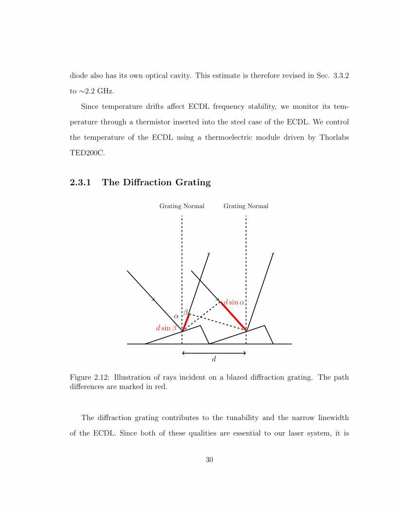
The diffraction grating contributes to the tunability and the narrow linewidth
of the ECDL. Since both of these qualities are essential to our laser system, it is
30

worthwhile to discuss the mechanism behind this frequency selection.
Light incident on a diffraction grating will be diffracted into a series of interference
patterns. Consider the geometry in the Fig. 2.12, where we show two grooves on the
surface of a blazed diffraction grating. The diffracted rays from adjacent grooves
(separated by d) interfere constructively when the total path difference between the
two rays shown in the figure is an integer multiple of the incident wavelength (λ), or
d(sinα− sin β) = mλ, (2.10)
where α and β represent the incident and diffracted angle with respect to the grating
normal and m is the integer diffraction order number.
If the diffracted light traces back to its incident direction, or α = −β, it is in
Littrow grating condition:
2d sinα = mλ. (2.11)
The feedback from the optical cavity formed between the rear crystal facet of the diode
and the diffraction grating enhances stimulated emission at the Littrow wavelength.
According to Eq. 2.11, changing the angle of incidence determines the wavelength
that satisfies the Littrow condition, which in turn determines the ECDL output.
In practice, we change the incident angle by tilting the grating normal. A piezo-
electric transducer is placed behind the grating mount to control the selection of
desired laser outputs. We use a blazed diffraction grating (Thorlabs GR-13-1208)
in our ECDL. With 1200 grooves per mm, the distance between adjacent grooves is
around 0.8µm. Considering the geometry of our diffraction mount, the diffraction
grating will be tilted at angle of 34.3◦ with respect to the external cavity axis in order
31

to select the 940nm beam. My calculations suggest that varying the laser wavelength
by 1FSR requires a piezo displacement of ∼ 30nm. This translates to a voltage of
around 2 volts for our Noliac piezo actuator (part number NAC2123-A01). In reality,
the piezo is less responsive than specified and requires much higher voltage.
2.4 System Performance
We successfully locked our ECDL to the HeNe using the setup presented in Sec. 2.1.
However, the actual frequency stability of the ECDL is determined by the stability
of the HeNe, the F-P cavity, and the precisions of the detection and software. This
means that we need a second frequency reference to assess the stability of the system
while it locks a laser to the HeNe. The mobile setup mentioned earlier in Sec. 2.2.2
conveniently allows us to adapt the laser lock to another laser. For testing purposes,
we use our system to stabilize the frequency of a laser (not our ECDL) that is resonant
with a thallium fluoride molecular transition in Professor Hunter’s lab.12 With this
setup, the molecular transition serves as the second frequency reference.
2.4.1 System Stability
A laser beam excites the thallium fluoride molecules from the ground state to one of
the excited states when its frequency corresponds to the energy difference between
the two internal states. Immediately following the excitation, spontaneous emissions
release photons that are counted with a photomultiplier. Since excitation is extremely
sensitive to laser frequency, the number of emitted photons changes drastically for
12The TlF transitions we observe are between the excited states (B3Π1(0)) and the various vibra-tional levels of the ground state (X1Σ+(ν)).[9]
32
small laser frequency drifts.
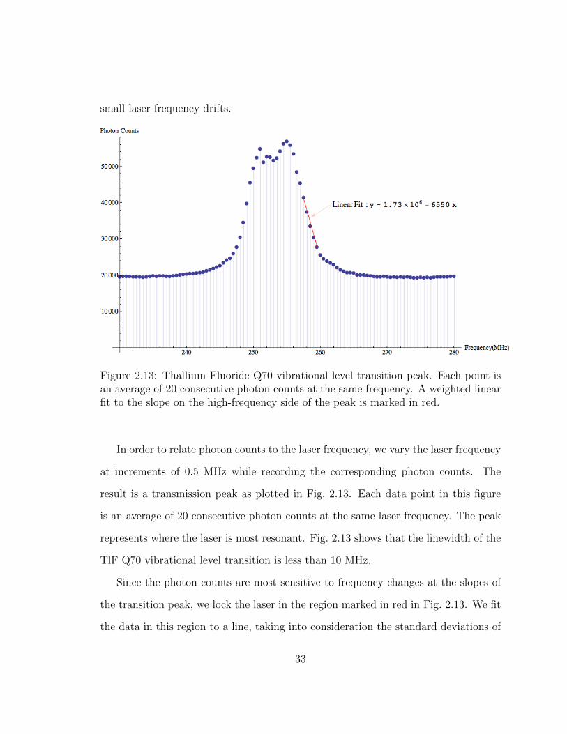
Figure 2.13: Thallium Fluoride Q70 vibrational level transition peak. Each point isan average of 20 consecutive photon counts at the same frequency. A weighted linearfit to the slope on the high-frequency side of the peak is marked in red.
In order to relate photon counts to the laser frequency, we vary the laser frequency
at increments of 0.5 MHz while recording the corresponding photon counts. The
result is a transmission peak as plotted in Fig. 2.13. Each data point in this figure
is an average of 20 consecutive photon counts at the same laser frequency. The peak
represents where the laser is most resonant. Fig. 2.13 shows that the linewidth of the
TlF Q70 vibrational level transition is less than 10 MHz.
Since the photon counts are most sensitive to frequency changes at the slopes of
the transition peak, we lock the laser in the region marked in red in Fig. 2.13. We fit
the data in this region to a line, taking into consideration the standard deviations of
33
each averaged photon count. The resulting fit parameters are used to convert photon
counts into frequency.
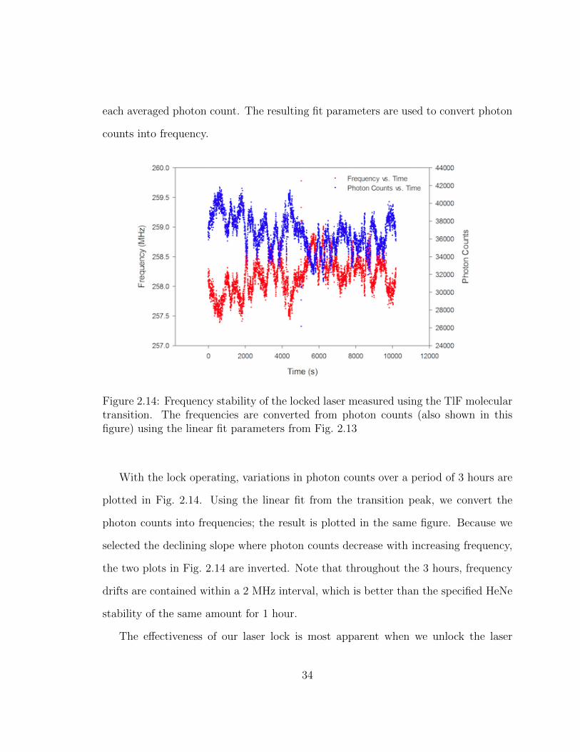
Figure 2.14: Frequency stability of the locked laser measured using the TlF moleculartransition. The frequencies are converted from photon counts (also shown in thisfigure) using the linear fit parameters from Fig. 2.13
With the lock operating, variations in photon counts over a period of 3 hours are
plotted in Fig. 2.14. Using the linear fit from the transition peak, we convert the
photon counts into frequencies; the result is plotted in the same figure. Because we
selected the declining slope where photon counts decrease with increasing frequency,
the two plots in Fig. 2.14 are inverted. Note that throughout the 3 hours, frequency
drifts are contained within a 2 MHz interval, which is better than the specified HeNe
stability of the same amount for 1 hour.
The effectiveness of our laser lock is most apparent when we unlock the laser
34

Figure 2.15: Laser frequency unlocked at the slope of the TlF Q70 transition peak.
frequency at the end of the 3 hour test. Fig. 2.15 shows that in a matter of seconds
the frequency drifts off the transition peak. Note that the flat tail at the end merely
represent background photon counts.
The Allan deviation plot is often used to show stability over different time scales.
To obtain Fig. 2.16, we first partition the data shown in Fig. 2.14 into all possible
bin sizes, which ranges from 2 seconds to about 1.5 hours. We then calculate the
standard deviation for each bin size.13 Notice that I have boxed out a region where
the Allan deviation declines before it become erratic. The decline shows that our
locking scheme is effectively controlling frequency drifts at a time scale of about 10
minutes. The erratic oscillations at the end of the plot is due to the increasing bin
size and decreasing number of bins used to calculate the standard deviations. The
13This calculation is explained in more detail in Appendix B.
35

Allan deviation plot shows that by using our locking system, the laser–and more
importantly the system–is stable to within 200 kHz over 3 hours. Our system is
performing exceedingly well!
2.4.2 Reaction to Temperature Drifts
When building the cavity, we emphasized the athermal design and the various features
added to isolate the cavity from its surroundings. We now test the merits of these
measures by observing how the system responds to temperature drifts.
We wrap a heater tape around the pressure chamber containing our F-P cavity.
The thermistor within the pressure chamber reports a linear change of temperature
at 0.003(1)oC/s. To keep this number in perspective, the normal temperature drift
Figure 2.16: Allan deviation of laser frequency in log-log scale. The Allan deviationin the boxed region indicates long term stability.
36

within the cavity as reported by the same thermistor is only around a factor of 100
less than this.
Figure 2.17: Frequency drift due to temperature change of the F-P cavity. Laserfrequency is locked throughout. The plot is fitted to a quadratic curve with theparameters attached to the figure.
Fig. 2.17 shows the frequency drift under a consistent temperature change while
the laser is locked. The system drifted over 1 MHz over 3oC. With a stability of
around 200 kHz, a temperature drift of ∼0.6oC will degrade the system. Since lab
temperature rarely fluctuates this much, the laser lock is, as planned, “athermal” for
small temperature variations.
The quadratic fit in Fig. 2.17 shows that the laser frequency seems to stabilize
towards the end at higher temperatures. We are not sure about the reason behind
this seemingly improving locking performance.
37

Figure 2.18: Laser power drift for the same time duration as Fig. 2.14.
2.4.3 The Other Factors
It is important to keep in mind that the detection of the emitted photons depend on
other factors, most notably incident laser power. Variations in these factors contribute
to the observed frequency drifts, which might exaggerate the actual frequency drifts.
Fig. 2.18 shows the laser power drift as we took the data in Fig. 2.14. We observe a
discontinuous change in laser power half way into the test. Since this fluctuation is
mirrored in the observed photon counts, the laser power drift may contribute to the
unusually noisy photon counts in this region.
So far we have been using photon counts observed by one of the detectors. There is
another detector that also tracks the number of emitted photons from the same group
of molecules. Since frequency drifts affect both detectors, photon counts from the two
detectors should correlate to each other if there are no other factors influencing the
38

Figure 2.19: Ratio of photon counts obtained by Channel A and Channel B.
photon counts.
In Fig. 2.19, we plot of ratio of photon counts observed by the two detectors over
time. The drift in the ratio demonstrates that there are other factors that influence
the two detectors in different ways.
The F-P locking system has demonstrated its ability to effectively stabilize laser
frequency by maintaining the long term laser stability at around 200 kHz. Moreover,
the various factors that might influence photon detection implies that the system
might actually perform even better than what we observed.
39

Chapter 3
Injection Current Modulation
Recall from Chapter 1 that efficient stimulated Raman transitions require a large
detuning, ∆, from the excited state. This large detuning complicates the process
of obtaining the six required laser beams from the stabilized ECDL laser. In this
chapter, we discuss a convenient method that can potentially be an alternative to
expensive electro-optical modulators (EOM’s), which have been shown to work for a
system similar to ours.[10]
Many groups have achieved frequency modulations above 7 GHz with more than
2 % of the carrier power in the first sideband through direct microwave modulations of
external cavity diode lasers. [11, 12] We followed a similar procedure and were able to
modulate our ECDL up to 6.6 GHz with 3 % of the carrier power in the first sideband.
We also investigated the dependence of modulation response on a variety of factors;
most of the observations confirm theoretical expectations. These observations can
help us to choose appropriate conditions to obtain an optical sideband suitable for
our experiments.
40

3.1 Experimental Setup
We implement injection current modulation using the setup illustrated in Fig. 3.1.
The DC bias current is combined with an rf signal1 through a bias T, and the super-
imposed signal is used to drive the laser diode. The modulated ECDL output is sent
to a scanning Fabry-Perot cavity similar to the one we built.2 We scan this F-P with
a triangle wave to observe the carriers and sidebands.
We make no attempt to impedance-match the rf power, but we monitor the re-
flected power using a directional coupler. The crystal detector measures the reflected
rf power, which can be used to gauge the actual rf power received by the laser diode.
RF Signal(Agilent 83650B)
DC Bias(Thorlabs LDC202C)
Bias TZFBT-6GW+
Directional Coupler(Narda 25288B)
ECDL
Laser Diode(M9-940-0150-D5P)
F-PCavity
Oscilloscope
Crystal Detector(HP 8472A)
Laser beam
Reflected rf Power
Figure 3.1: Experimental setup for injection current modulation. The rf signal iscombined with the DC bias current through the bias T. The directional coupler picksup the reflected rf power, which is measured by the crystal detector. The modulatedlaser output is analyzed by a scanning F-P cavity. Part numbers are attached whenapplicable.
1The rf signal generator is provided by the Friedman Lab.2This F-P cavity is from the DeMille group at Yale University; it is also a confocal cavity with an
athermal design. In fact, we borrowed the design for our F-P cavity from this model. As discussedin Chapter 2, this cavity has a higher finesse of above 1500 and an FSR of 500 MHz.
41
3.2 Supporting Theory
Sinusoidal modulation of the injection current causes sinusoidal response of the output
electric field. Both amplitude and frequency modulation (AM and FM) result, and
optical sidebands appear in the output of the laser.
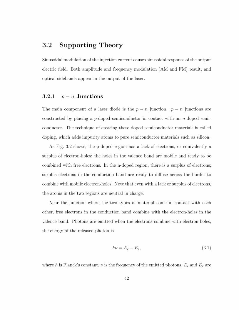
3.2.1 p− n Junctions
The main component of a laser diode is the p − n junction. p − n junctions are
constructed by placing a p-doped semiconductor in contact with an n-doped semi-
conductor. The technique of creating these doped semiconductor materials is called
doping, which adds impurity atoms to pure semiconductor materials such as silicon.
As Fig. 3.2 shows, the p-doped region has a lack of electrons, or equivalently a
surplus of electron-holes; the holes in the valence band are mobile and ready to be
combined with free electrons. In the n-doped region, there is a surplus of electrons;
surplus electrons in the conduction band are ready to diffuse across the border to
combine with mobile electron-holes. Note that even with a lack or surplus of electrons,
the atoms in the two regions are neutral in charge.
Near the junction where the two types of material come in contact with each
other, free electrons in the conduction band combine with the electron-holes in the
valence band. Photons are emitted when the electrons combine with electron-holes,
the energy of the released photon is
hν = Ec − Ev, (3.1)
where h is Planck’s constant, ν is the frequency of the emitted photons, Ec and Ev are
42
p-doped n-doped
Neutral region Neutral region
Depletion region E-field
- -
- -- -- -
- -+ +
+ ++ ++ +
+ +
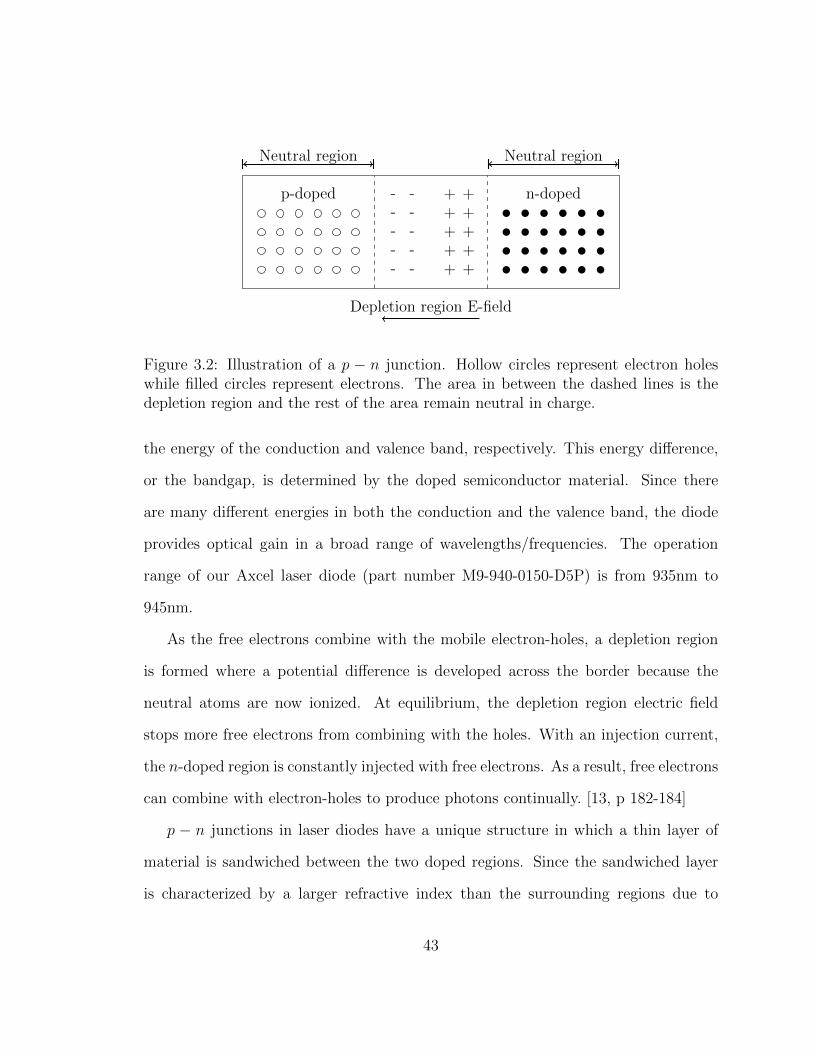
Figure 3.2: Illustration of a p − n junction. Hollow circles represent electron holeswhile filled circles represent electrons. The area in between the dashed lines is thedepletion region and the rest of the area remain neutral in charge.
the energy of the conduction and valence band, respectively. This energy difference,
or the bandgap, is determined by the doped semiconductor material. Since there
are many different energies in both the conduction and the valence band, the diode
provides optical gain in a broad range of wavelengths/frequencies. The operation
range of our Axcel laser diode (part number M9-940-0150-D5P) is from 935nm to
945nm.
As the free electrons combine with the mobile electron-holes, a depletion region
is formed where a potential difference is developed across the border because the
neutral atoms are now ionized. At equilibrium, the depletion region electric field
stops more free electrons from combining with the holes. With an injection current,
the n-doped region is constantly injected with free electrons. As a result, free electrons
can combine with electron-holes to produce photons continually. [13, p 182-184]
p − n junctions in laser diodes have a unique structure in which a thin layer of
material is sandwiched between the two doped regions. Since the sandwiched layer
is characterized by a larger refractive index than the surrounding regions due to
43
the choice of low-bandgap materials, the recombinations are confined within a small
depletion region known as the active layer. [14, p 82] As injection current increases,
an increasing number of electrons are confined to the active layer to allow stimulated
emissions.
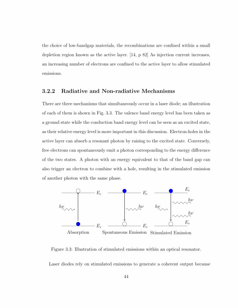
3.2.2 Radiative and Non-radiative Mechanisms
There are three mechanisms that simultaneously occur in a laser diode; an illustration
of each of them is shown in Fig. 3.3. The valence band energy level has been taken as
a ground state while the conduction band energy level can be seen as an excited state,
as their relative energy level is more important in this discussion. Electron-holes in the
active layer can absorb a resonant photon by raising to the excited state. Conversely,
free electrons can spontaneously emit a photon corresponding to the energy difference
of the two states. A photon with an energy equivalent to that of the band gap can
also trigger an electron to combine with a hole, resulting in the stimulated emission
of another photon with the same phase.
Ev
Ec
Absorption
hν
Ev
Spontaneous Emission
Ec
hν
Ev
Ec
Stimulated Emission
hν
hν
hν
Figure 3.3: Illustration of stimulated emissions within an optical resonator.
Laser diodes rely on stimulated emissions to generate a coherent output because
44

stimulated emissions can quickly increase the number of photons that are in phase
with each other. Stimulated emissions can only dominate once the electron density
in the active layer exceeds a certain threshold called the transparency value. Beyond
the threshold with a DC injection current, the net rate of stimulated emission per
photon(G) is proportional to the number of electrons(N) in the active layer:
G = g(N −NT ), (3.2)
where g is a constant and NT is the number of electrons at transparency value. For
a typical laser diode, the rate of spontaneous emission(Rsp) also varies linearly with
G by a proportionality constant of around 2. [14, p 107]
Optical gain alone is not enough for laser operation. Remember that a laser diode
also consists of an optical cavity formed by the two cleaved laser facets. The lasing
threshold is met when optical gain exactly compensates for the cavity loss due to
the imperfect reflectivity of the facets. The injection current needed to reach the
threshold gain is called the threshold current(Ith).
3.2.3 The Rate Equations
For a single-mode laser diode, its dynamics follow a set of differential equations called
the rate equations characterized by the photon number P and the electron number
N [14, p 107] :
dP
dt= GP +Rsp −
P
τp, (3.3)
dN
dt=I
e−GP − N
τc. (3.4)
45

In Eq. 3.3, the changes in photon count are determined by three terms: the net
increase in photons emitted due to stimulated emissions, the generation of photons
due to spontaneous emissions, and the net loss of photons determined by the lifetime
τp of the photons. In Eq. 3.4, the changes in electron number are also determined
by three terms: the first term gives the number of injected electrons obtained from
dividing the injection current I by the elementary charge e, the second term takes
into account the loss of electrons due to stimulated emissions, and the last term
represents the loss of electrons due to both spontaneous emissions and nonradiative
recombinations with τc as the carrier lifetime. Nonradiative recombinations refer to
the recombinations of the electrons and holes that result in phonon emissions (i.e.
semiconductor crystal lattice vibrations).
We are interested in solving the rate equations with a modulated injection current
in the form of Ib + Im cosωt, where Ib is the DC bias current and Im is the magnitude
of the radio frequency modulation. As a pair of coupled differential equations, the
rate equations can only be solved numerically. However, we can obtain an analytic
solution by making the small signal approximation given that our modulation signal
fulfills the following condition [14, p 110]:
Im � Ib − Ith, (3.5)
where Ith is the threshold current.
When the injection current is modulated, the net rate of stimulated emission per
photon G is no longer linearly dependent on the number of electrons in the active layer
46

as described in Eq. 3.2. The following equation offers a more realistic description:
G = g(N −NT )(1− εNLP ), (3.6)
where εNL is a non-linear gain parameter that is typically ≈ 10−7. This modified
expression reflects the dependency of the gain on both the electron and photon number
during injection current modulation.
With a small sine wave modulation, the rate equations can be linearized and solved
using the small-signal approximation and the Fourier-transform technique to give a
set of general solutions [15, p 84]:
P (t) = 〈P 〉+ Re[∆Peiωmt], (3.7)
N(t) = 〈N〉+ Re[∆Neiωmt]. (3.8)
The number of electrons and photons vary sinusoidally around their mean values
〈N〉 and 〈P 〉 at a frequency equivalent to the modulation frequency ωm. To make
this relationship a little more intuitive, one can take a look again at the rate equa-
tions. The injection current clearly affects the electron number from the second rate
equation. The photon number is related to the injection current through G, which is
related to both P and N according to Eq. 3.6.
Furthermore, given the modulated electron number in Eq. 3.8, the optical fre-
quency ν is also directly modulated[15, p 121]:
ν = 〈ν〉+ Re[∆νeiωmt], (3.9)
47

where 2πν = ω. This result follows from the dependence of optical frequency on
the refractive index and the group refractive index. Since the crystal surfaces of the
active layer effectively serve as an optical resonator, the refractive index determines
the possible emission frequencies and it changes rather linearly with electron numbers.
On the other hand, the group refractive index concerns with the spacing between
two adjacent emission frequencies (also called longitudinal mode spacing); it varies
with the non-linear stimulated emission gain, which contributes to the non-linear
modulation response of the optical frequency. [15, p 31-32]
While the electric field might be directly modulated in externally modulated sys-
tems, it is important to realize that the output power rather than the electric field is
modulated during injection current modulation. [16] Therefore in our case,
P ∝ |E(t)|2, (3.10)
where P is again the photon number and E(t) is the electric field of the output
optical wave. When deriving the electric field expressions for the optical sidebands
in Sec. 3.2.6, this relationship will result in a square root for the electric field due to
amplitude modulation.
Eq. 3.7 and Eq. 3.9 show that injection current modulation leads to both amplitude
modulation and frequency modulation. It is in principle possible to predict the relative
amount of AM vs. FM by solving the rate equations, but the diodes are typically not
documented sufficiently for useful calculations. In practice, we can infer their relative
strengths from the modulated sideband intensities.
48

3.2.4 The AM Theory
Before deriving the expression for optical sidebands, it is helpful to consider amplitude
modulation and frequency modulation separately.
Consider a carrier wave c(t) with frequency ωc and amplitude Ac such that c(t) =
Ac cos(ωct). The amplitude of the carrier is modulated by the signal s(t) = Am cos(ωmt),
where Am is the amplitude of the modulated signal and ωm is the modulation fre-
quency.
The effect of amplitude modulation is that the carrier amplitude at each moment
is modified by the instantaneous value of the modulated signal. [17, p 94-96] In other
words, the carrier amplitude is no longer constant: it is now Ac + s(t). This new
amplitude leads to a new expression for the modulated carrier wave:
cAM(t) = [Ac + Am cos(ωmt)] cos(ωct). (3.11)
Multiplying out each term within the parenthesis with cos(ωct) and using trigono-
metric identities, Eq. 3.11 can be rewritten as
cAM(t) = Ac cos(ωct) +Am2
cos(ωc − ωm)t+Am2
cos(ωc + ωm)t. (3.12)
This equation shows that amplitude modulation with a single modulation frequency
results in two sidebands (the second and third term in Eq. 3.12). Their amplitudes
have the same signs and their frequencies differ from the carrier frequency by the
modulation frequency.
49

3.2.5 The FM Theory
Frequency modulation is similar to phase modulation because both cause phase
changes in the resulting output. Unlike phase modulation, which directly vary the
phase of the carrier, in frequency modulation the phase change is a result of changes
in the instantaneous frequency of the carrier. Consider the same sinusoidal carrier
signal c(t) from section 3.2.4, and the same modulation signal s(t) except this time
as frequency modulation. The instantaneous phase θFM(t) in frequency modulation
is obtained by taking the integral of the modulation signal:
θFM(t) = ωct+
∫ t
t0
s(t) dt, (3.13)
where the lower integral limit is the time at the beginning of frequency modulation.
Since our modulation signal is a cosine wave, the instantaneous phase can be
solved, and the modulated signal becomes
cFM(t) = Ac cos(ωct+f
ωmsinωmt), (3.14)
where f has units of angular frequency.
Unlike the case of amplitude modulation, Eq. 3.14 theoretically contains infinite
sidebands when expanded into a Fourier series. The details of the expansion will soon
be discussed along with injection current modulated sidebands.
50

3.2.6 Optical Sidebands
In Sec. 3.2.3 we established that under a small-signal modulation of the injection
current, the output power and frequency respond sinusoidally. If we superpose a DC
bias current Ib with an RF signal Im cosωmt, making sure that Im � Ib−Ith, the AM
and FM theory derived in section 3.2.4 and section 3.2.5 are now ready to be applied.
Take the original electric field with just the bias current to be the carrier. The
carrier can be written in complex exponential form for convenience: E0eiω0t, where E0
is the carrier amplitude and ω0 is the carrier frequency. Here, the real part corresponds
to the physical electric field. According to Eq. 3.11 and Eq. 3.14, the electric field
resulting from each kind of modulation independently would be
EAM(t) = E0eiω0t√
(1 +M cosωmt) (3.15)
and
EFM(t) = E0ei(ω0t+β sinωmt), (3.16)
respectively, where M is the degree of AM modulation and β is the FM modulation
index. As mentioned before, the square root in Eq. 3.15 results from the output power
instead of the electric field being directly modulated by the injection current.
Fourier expanding the frequency modulated electric field leads to the following
51

series[18]:
E0ei(ω0t+β sinωmt) =J0(β)E0e
iω0t
+ J1(β)E0ei(ω0t+ωmt) − J1(β)E0e
i(ω0t−ωmt)
+ J2(β)E0ei(ω0t+2ωmt) + J2(β)E0e
i(ω0t−2ωmt)
+ ...
+ Jl(β)E0ei(ω0t+lωmt) + (−1)lJl(β)E0e
i(ω0t−lωmt).
(3.17)
Each term in the series contains Jl(β), or the Bessel functions of the first kind. The
Bessel functions are functions of a single variable, in our case the modulation index
β.
In Eq. 3.17, the first line refers to the carrier, the second line contains the first
and minus first sidebands, and so on. Unlike amplitude modulation, sidebands due
to pure frequency modulation are alternately in phase and out of phase.
The amplitudes of the carrier and the sidebands are determined by the Bessel
functions. Fig. 3.4 shows the first three orders of the Bessel functions. As expected,
with no modulation, J0(0) is unity and the carrier wave is at its full amplitude. For
our experiments, we have β < 1 mostly because of the low rf power received by the
laser diode. In this range, the amplitudes of the sidebands increase as β increases.
Higher sidebands are suppressed due to the low amplitudes of the higher order Bessel
functions.
Since modulating the injection current causes both amplitude and frequency mod-
ulation, combining Eq. 3.15 and Eq. 3.16 leads to the general modulated electric
52

Figure 3.4: The first three orders of the Bessel functions.
field[16]:
E(t) = E0ei(ω0t+β sinωmt)
√1 +M cos(ωmt). (3.18)
This expression shows that the amplitudes of each pair of the frequency modu-
lated sidebands are modified by amplitude modulation. A second order expansion
of Eq. 3.18 gives an approximation of the first few sidebands:
Carrier : E0eiω0t[J0(β)(1− M2
16)− J2(β)
M2
16];
+1 : E0ei(ω0t+ωmt)[J0(β)
M
4+ J1(β)(1− M2
32) + J2(β)
M
4];
-1 : E0ei(ω0t−ωmt)[J0(β)
M
4− J1(β)(1− M2
32) + J2(β)
M
4];
+2 : E0ei(ω0t+2ωmt)[−J0(β)
M2
32+ J1(β)
M
4+ J2(β)(1− M2
16)];
-2 : E0ei(ω0t−2ωmt)[−J0(β)
M2
32− J1(β)
M
4+ J2(β)(1− M2
16)].
(3.19)
53

These expressions are derived in Appendix A.
Further reducing Eq. 3.19 by ignoring terms containing M2 gives a set of simpler
expressions:
Carrier : E0eiω0tJ0(β);
+1 : E0ei(ω0t+ωmt)[J0(β)
M
4+ J1(β) + J2(β)
M
4];
-1 : E0ei(ω0t−ωmt)[J0(β)
M
4− J1(β) + J2(β)
M
4];
+2 : E0ei(ω0t+2ωmt)[J1(β)
M
4+ J2(β)];
-2 : E0ei(ω0t−2ωmt)[−J1(β)
M
4+ J2(β)].
(3.20)
This set of approximations differ from the ones derived from directly modulating the
electric field instead of the power by a factor of 1/2 in the terms related to amplitude
modulation.[18]
Since a photodetector measures intensity rather than electric field, the relative
intensity of each sideband can be obtained by taking the absolute value squared of
the respective electric field and dividing by the absolute value squared of the carrier
electric field. Experimental observations of any two sideband intensities relative to
that of the carrier will be sufficient for solving both β and M .
3.3 Experimental Observations
According to Sec. 3.2.6, first sidebands have a frequency of f0 + fm while minus
first sidebands have a frequency of f0 − fm, where f0 is the carrier frequency and
fm is the modulation frequency. Fig. 3.5 shows the transmission peak positions as
54

−1α α +1α β−1β +1β −1γ γ +1γ
FSR
FSR
ωm
ωm
−1β α +1 −1γ β +1α −1 γ +1β
fm
fm + FSR
Figure 3.5: An illustration of sideband positions for different modulation frequen-cies. α, β, γ denote carrier peaks as we scan the F-P cavity, the distance betweenadjacent carriers is the FSR. +1 and -1 are first and minus first sidebands and theirsubscripts indicate the corresponding carriers. The sidebands are seperated from thecorresponding carriers by the modulation frequency.
we scan the F-P cavity by more than two FSRs. Notice that when we increase the
modulation frequency by one FSR, some sidebands (+1γ and −1α) are off the screen.
We still see the same sideband pattern because sidebands from other carriers fill in
their positions. This analysis demonstrates that the F-P cavity registers the same
pattern for modulation frequencies that differ by an integer number of the FSR.
Since the first and minus first sidebands are symmetrically spaced with respect
to the carrier, they overlap for fm at integer multiples of 250 MHz if our cavity FSR
55

is actually 500 MHz. This allows us to measure the FSR of our cavity by observing
the modulation frequency for which the first and minus first sidebands overlap. In
Fig. 3.6, the first and minus first sidebands overlap exactly for fm = 2750 MHz,
confirming that our FSR is 500 MHz.
Figure 3.6: Sidebands modulated at 2750 MHz. The first and minus first sidebandscoincide at the center between two carrier peaks.
Fig. 3.7 shows another observation that is consistent with theoretical predictions.
We mentioned in Sec. 3.2.4 that injection current modulation results in both AM and
FM. The AM modulation causes uneven power in the first and minus first sidebands,
which is evident in Fig. 3.7. Also note that the power of negative sidebands is always
less than that of positive sidebands according to the expanded expressions for the
sidebands in Sec. 3.2.6.
Now that we know our setup works, recall that our goal is two-fold: we want to
56
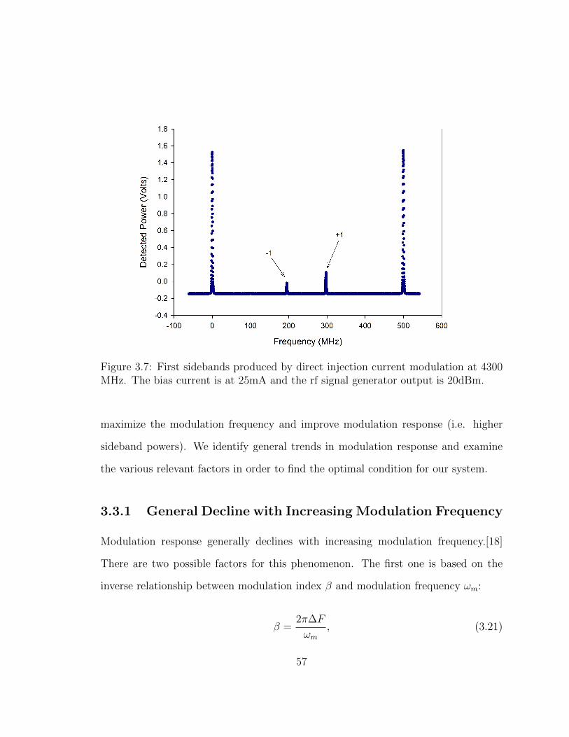
Figure 3.7: First sidebands produced by direct injection current modulation at 4300MHz. The bias current is at 25mA and the rf signal generator output is 20dBm.
maximize the modulation frequency and improve modulation response (i.e. higher
sideband powers). We identify general trends in modulation response and examine
the various relevant factors in order to find the optimal condition for our system.
3.3.1 General Decline with Increasing Modulation Frequency
Modulation response generally declines with increasing modulation frequency.[18]
There are two possible factors for this phenomenon. The first one is based on the
inverse relationship between modulation index β and modulation frequency ωm:
β =2π∆F
ωm, (3.21)
57
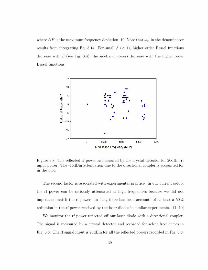
where ∆F is the maximum frequency deviation.[19] Note that ωm in the denominator
results from integrating Eq. 3.14. For small β (< 1), higher order Bessel functions
decrease with β (see Fig. 3.4); the sideband powers decrease with the higher order
Bessel functions.
Figure 3.8: The reflected rf power as measured by the crystal detector for 20dBm rfinput power. The -16dBm attenuation due to the directional coupler is accounted forin the plot.
The second factor is associated with experimental practice. In our current setup,
the rf power can be seriously attenuated at high frequencies because we did not
impedance-match the rf power. In fact, there has been accounts of at least a 50 %
reduction in the rf power received by the laser diodes in similar experiments. [11, 19]
We monitor the rf power reflected off our laser diode with a directional coupler.
The signal is measured by a crystal detector and recorded for select frequencies in
Fig. 3.8. The rf signal input is 20dBm for all the reflected powers recorded in Fig. 3.8.
58

Surprisingly, only as much as 10 % of the incident power is reflected back. However,
given the amount of modulation we observe in the sidebands, it is unlikely that all of
the remaining power goes into the laser diode. One way to potentially increase the rf
power received by the laser diode is to increase the incident rf power. Unfortunately,
the rf signal output in our setup cannot exceed 20dBm. For future experiments, it
might be helpful to use an rf generator with higher output power.
Figure 3.9: First sidebands modulation depths at different modulation frequencies forDC bias at 55mA. We were only able to observe sidebands at modulation frequenciescorresponding to the data points plotted in this figure.
We observe the relative power of the first and minus first sidebands with respect
to the carrier (i.e. the modulation depth) for various modulation frequencies. The
modulation depths for the first sidebands are plotted in Fig. 3.9. Using the expressions
for the carrier, first sidebands, and minus first sidebands from Sec. 3.2.6, we can
calculate the AM and FM modulation indices. The results are plotted in Fig. 3.10.
59

Figure 3.10: FM indices(β) and AM indices(M) for modulation frequencies from 15-6650 MHz. The DC bias current is at 55mA for all data points. Note that missingdata points correspond to β and M ∼ 0 at those modulation frequencies.
In Fig. 3.10 and Fig. 3.9, the peak heights decline with increasing frequency, sup-
porting the discussion above. The exception at around 100 MHz and the dramatic
response at certain frequencies are due to another phenomenon discussed in the fol-
lowing section.
3.3.2 Dramatic Improvements from External Cavity Feed-
back
Because of the constructive feedback provided by the external cavity in an ECDL,
there is a strong correlation between modulation response and the free spectral range
(FSR) of the external cavity.[18–20] More specifically, optimal modulation depth is
60

achieved with fm at integer multiples of the external cavity FSR.
This dramatic improvement in modulation response is prominent in Fig. 3.10 and
Fig. 3.9. Although in the previous section we discussed about reduced modulation
responses at higher modulation frequencies, the cavity feedback allows better modu-
lation responses at 2 GHz and at 4.5 GHz than those at sub-FSR frequencies.
Because Fig. 3.10 and Fig. 3.9 are quite noisy, which might be partly because of the
fluctuations in the rf power, we cannot extrapolate from them with much precision
our actual external cavity FSR. Nonetheless, since the modulation responses peak
consistently below the expected frequencies for the FSR at 2.4 GHz, 2.2 GHz is
probably a better estimate.
3.3.3 Bias Current Dependence
There have been several observations of improved modulation response upon de-
creasing the bias current.[11, 19, 20] In some cases, the modulation depths are quite
sensitive to how far the current is above threshold. [11]
There are two possible explanations for this phenomenon. First, when decreasing
the bias current (while still remaining above the threshold current), the fractional
modulation amplitude given the same rf power increases. This leads to an increase
in β, which improves modulation response.
Second, the parasitic capacitance in laser diodes might filter out high frequency
rf signals.[15, p 93-94] As a potential develops between the two doped semiconductor
regions (explained in Sec. 3.2.1), the p− n junction becomes analogous to a parallel
plate capacitor. If we approximate a laser diode as a diode connected in parallel with
a capacitor, the laser diode becomes effectively a low-pass filter. Lowering the DC
61

bias current can reduce the parasitic capacitance and allow higher frequency rf signals
to enter the diode, improving the modulation response.
We vary the bias current at fm = 4300 MHz and at fm = 6644 MHz, where
we observed maximum modulation response according to Fig. 3.10. Since our laser
current threshold is 18mA, we start the bias current at 20mA. For fm = 4300 MHz,
Fig. 3.12 and Fig. 3.11 show that modulation response generally decays as we increase
the bias current. There is a local maximum around 55mA for both AM and FM
indices, and the corresponding modulation depth is around 10 %.
At fm = 6644 MHz, Fig. 3.13 and Fig. 3.11 indicate maximum modulation re-
sponse at around 50mA. There is a greater bias current dependence of the AM indices
than the FM indices. While modulation response almost linearly increases with de-
Figure 3.11: Bias current dependence of modulation depth at fm =4300 MHz. Linearfit slope is attached.
62

Figure 3.12: Bias current dependence of modulation indices at fm =4300 MHz.
creasing bias current for fm = 4300 MHz, at fm = 6644 MHz the modulation response
declines both at low and high bias currents. We attempt to explain this difference in
the following section.
3.3.4 Frequency of Oscillation Relaxations
There is an upper limit on modulation frequency for each laser diode. This is de-
termined by the frequency of relaxation oscillations, which is related to how fast the
laser diode can return to its steady-state under current disturbances. In general,
modulation efficiency decreases dramatically as the modulation frequency increases
far above the frequency of relaxation oscillations. [14, p 144]
The frequency of relaxation oscillations in some diode lasers has been documented
to range from 2 to 5 GHz. [14, p 210] In our case, we were not able to observe any
63

Figure 3.13: Bias current dependence of modulation indices at fm =6644 MHz.
Figure 3.14: Bias current dependence of modulation depth at fm =6644 MHz.
64
sidebands after 6650 MHz. The next external cavity feedback is at least above 8 GHz,
which might exceed the frequency of oscillation relaxations by too much to allow for
any modulation response.
We have mentioned the improved modulation responses with lower bias current.
This improvement is counteracted, however, by the dependence of the frequency of
relaxation oscillations (fr) on the bias current (I). This relationship is expressed in
the following equation:
fr =
√I/Ith − 1
τcτp, (3.22)
where Ith is the threshold current, τc and τp are the carrier and photon lifetimes,
respectively.[19]
Eq. 3.22 might explain the difference in the bias current dependence of modulation
responses observed for 4300 MHz and 6644 MHz (compare Fig. 3.11 and Fig. 3.14).
As the bias current decreases, fr also decreases, lowering the the upper limit of the
modulation frequency. Hence we observe a decline in modulation response for 6644
MHz at low bias currents. For bias current at 50mA, we obtain 3 % modulation depth
for the first sidebands at fm =6.6 GHz. Without considering the absolute powers of
the carrier and the sidebands, this seems to be the optimal condition for our system.
3.3.5 Mysterious Sidebands
So far we have examined observations that are consistent with theoretical expecta-
tions. We also encountered a puzzling situation where unexpected sidebands appear
at 0.5fm away from the carrier frequency. These “half sidebands” persist between
fm =4243 MHz and fm =4309 MHz. While the theory only predicts integer side-
65

bands, the “half-sidebands” in Fig. 3.15 appear AM and FM modulated.
We also found that at fm =4266 MHz, the diode is destabilized. Perhaps there is a
connection between these two phenomena, but we have not yet found an explanation
for it.
Figure 3.15: Sidebands modulated at 4257 MHz. The dashed lines mark the positionsof the hypothetical “half sidebands”.
While these “half sidebands” are unexpected, they are not serious concerns given
what we need. We have demonstrated that our diode laser can be modulated up to
6.6 GHz and that its relative power with respect to the carrier can be adjusted with
the DC current. The power in the optical sideband is likely enough if we use them
as resonant beams so that the non-resonant (Raman) beams can benefit from the
larger power of the carrier. Hopefully, the detuning generated using injection current
modulation is large enough for Raman transitions.
66

Chapter 4
Conclusion
We have built a laser lock that automates frequency stabilization. According to a
thallium fluoride molecular transition, the system is stable to within 200 kHz over 3
hours. Since the system depends on the stability of the Fabry-Perot cavity, we took
measures to isolate the cavity from acoustic vibrations and pressure and temperature
variations. We showed that our system is resistant to temperature changes below
0.6oC. For usual lab temperature drifts, our system is practically athermal. This
setup is complete and mounted on a 1’ × 2’ mobile breadboard, designed to be
conveniently incorporated into laser systems with fiber-coupled outputs. We have
used this laser lock to successfully stabilize the frequency of our external cavity diode
laser.
For injection current modulation, we have demonstrated that our ECDL can be
most effectively modulated at frequencies around 2.2 GHz, 4.4 GHz, and 6.6 GHz due
to the enhanced external cavity feedback. We observed a strong correlation between
the modulation response and the bias current. At 6.6 GHz, the optimal bias current
67

is at 50mA, where we obtain 3 % of the output power in the sideband. Although we
had originally hoped to modulate the laser diode at 9.6 GHz, we believe that a 6.6
GHz detuning could also allow us to implement Raman transitions for the sideband
cooling. Its efficiency of course awaits to be tested on the logic ions.
An immediate next step is to convert both the carrier and the sideband to the
ultraviolet. Celia Ou has designed a frequency conversion setup and it is still in the
construction stage. After frequency conversion, the carrier and the sideband need
to be modulated by acousto-optic modulators to generate a total of 6 laser beams.
The carrier will be modulated to produce the two Raman beams separated by around
1.25 GHz. The sideband will be the source of the Doppler beams, repump laser,
and detection laser. Once the logic ions are trapped, these six beams can potentially
accomplish the second step we mentioned in Chapter 1, preparing the logic ions for
manipulating the spectroscopy ions.
68

Appendix A
Optical Sideband Derivations
The goal is to expand
E(t) = E0ei(ω0t+β sinωmt)
√1 +M cos(ωmt). (A.1)
The following expansions are taken from ref. [21]:
(1 + x)α = 1 + αx+α(α− 1)
2!x2 +
α(α− 1)(α− 2)
3!x3 + ...+
(α
n
)xn, (A.2)
where the interval of convergence is −1 < x < 1.
cos2nx =1
22n−1
n−1∑k=0
(2n
k
)cos(2n− 2k)x+
(2n
n
)1
22n(A.3)
and
cos2n−1x =1
22n−2
n−1∑k=0
(2n− 1
k
)cos (2n− 2k − 1)x. (A.4)
Since we are modulating the injection current with a small signal, assume |M | < 1
69

and the square root term in Eq. A.1 can be rewritten as
1 +1
2M cos(ωmt)−
1
8M2cos2(ωmt) +
1
16M3cos3(ωmt) + ...+
∞∑n
(12
n
)Mncosn(ωmt).
(A.5)
Expanding the first few terms of Eq. A.5 using Eq. A.3 and Eq. A.4 leads to
1 +1
2M cos(ωmt)
− 1
16M2 − 1
16M2 cos(2ωmt)
+1
64M3 cos(3ωmt) +
3
64M3 cos(ωmt)
+ ...
(A.6)
For convenience, cosines can also be written in complex exponential form so that the
first three lines of Eq. A.6 become
1 +1
4Meiωmt +
1
4Me−iωmt
− 1
16M2 − 1
32M2e2iωmt − 1
32M2e−2iωmt
+1
128M3e3iωmt +
1
128M3e−3iωmt +
3
128M3eiωmt +
3
128M3e−iωmt.
(A.7)
70

Recall from Chapter 3 that using Fourier expansion,
ei(ω0t+β sinωmt) = J0(β)E0eiω0t
+ J1(β)E0ei(ω0t+ωmt) − J1(β)E0e
i(ω0t−ωmt)
+ J2(β)E0ei(ω0t+2ωmt) + J2(β)E0e
i(ω0t−2ωmt)
+ ...
+ Jl(β)E0ei(ω0t+lωmt) + (−1)lJl(β)E0e
i(ω0t−lωmt),
(A.8)
where Jl(β) is the lth order Bessel function of the first kind.
Combining Eq. A.7 and Eq. A.8 and neglecting all terms smaller than M2 gives
the second order expansion of the first few sidebands:
Carrier : E0eiω0t[J0(β)(1− M2
16)− J2(β)
M2
16];
+1 : E0ei(ω0t+ωmt)[J0(β)
M
4+ J1(β)(1− M2
32) + J2(β)
M
4];
-1 : E0ei(ω0t−ωmt)[J0(β)
M
4− J1(β)(1− M2
32) + J2(β)
M
4];
+2 : E0ei(ω0t+2ωmt)[−J0(β)
M2
32+ J1(β)
M
4+ J2(β)(1− M2
16)];
-2 : E0ei(ω0t−2ωmt)[−J0(β)
M2
32− J1(β)
M
4+ J2(β)(1− M2
16)].
(A.9)
71
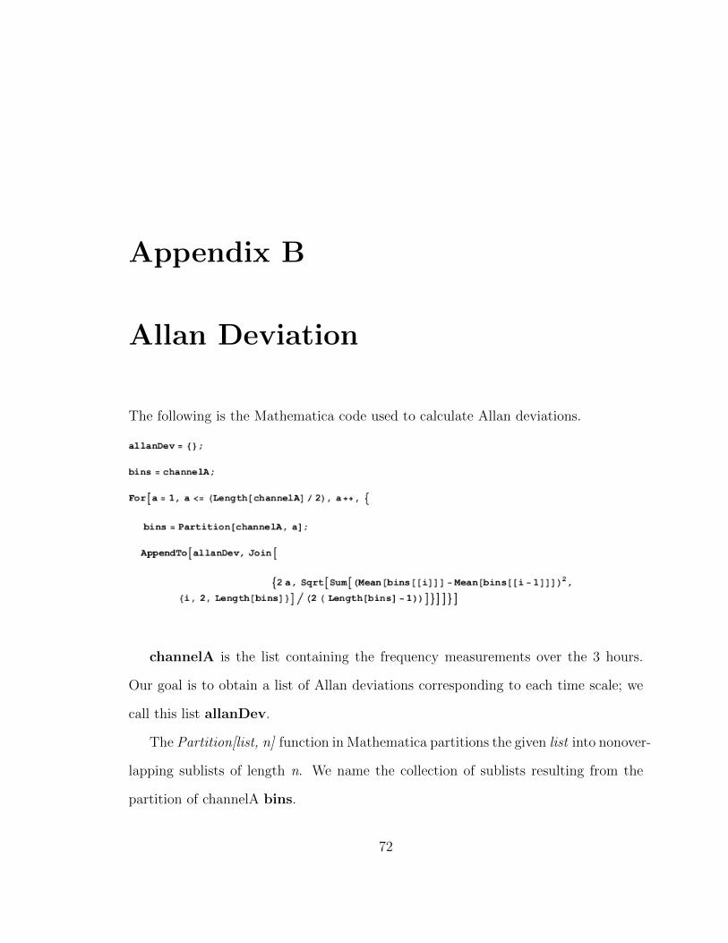
Appendix B
Allan Deviation
The following is the Mathematica code used to calculate Allan deviations.
channelA is the list containing the frequency measurements over the 3 hours.
Our goal is to obtain a list of Allan deviations corresponding to each time scale; we
call this list allanDev.
The Partition[list, n] function in Mathematica partitions the given list into nonover-
lapping sublists of length n. We name the collection of sublists resulting from the
partition of channelA bins.
72

The loop successively partitions channelA into bins containing less and less data
points. At each step, the loop calculates the Allan deviation with the Sqrt[...] term.
The loop starts from having 1 bin and stops at a bin number corresponding to 2
data points in each bin. I use the Join[...] function to time-stamp each calculated
Allan deviation using the fact that each measurement took 2 seconds. The resulting
allanDev is a list containing Allan deviations(MHz) vs. time(s).
73

Bibliography
[1] J.-P. Uzan, “The Fundamental Constants and Their Variation: Observational
Status and Theoretical Motivations,” Rev.Mod.Phys. (2002).
[2] S. Qiao, “Constructing a Linear Paul Trap System for Measuring Time-variation
of the Electron-Proton Mass Ratio,” Amherst College Undergraduate Thesis
(2013).
[3] C. Ou, “Third Harmonic Conversion,” Amherst College Undergraduate Thesis
(2013).
[4] R. B. Blakestad, Transport of Trapped-Ion Qubits within a Scalable Quantum
Processor, Ph.D. thesis, University of Colorado (2010).
[5] D. Wineland, M. Barrett, J. Britton, J. Chiaverini, B. DeMarco, W. Itano,
B. Jelenkovic, C. Langer, D. Leibfried, V. Meyer, T. Rosenband, and T. Schatz,
“Quantum Information Processing with Trapped Ions,” Phil. Trans. Royal Soc.
London A (2003).
[6] J. T. Verdeyen, Laser Electronics (Prentice-Hall, Inc., New York, 1981).
74
[7] D. C. Sinclair, “Scanning Spherical-Mirror Interferometers For The Analysis of
Laser Mode Structure,” Spectra-Physics laser Technical Bulletin (1968).
[8] S. D. Saliba, M. Junker, L. D. Turner, and R. E. Scholten, “Mode Stability of
External Cavity Diode Lasers,” Optical Society of America (2009).
[9] N. S. Wadia, “Measurements of Branching Ratios for the B(0)-X(ν) Transition
in Thallium Fluoride to Determine its Potential for Laser Cooling,” Amherst
College Undergraduate Thesis (2013).
[10] B. Hemmerling, F. Gebert, Y. Wan, and D. Nigg, “A single laser system for
ground-state cooling of 25Mg+,” Applied Physics B (2011).
[11] C. J. Myatt, N. R. Newbury, and C. E. Wieman, “Simplified Atom Trap By
Using Direct Microwave Modulation Of A Diode Laser,” Optics Letters 18, 649
(1993).
[12] R. Kowalski, S. Root, S. D. Gensemer, and P. L. Gould, “A Frequency-Modulated
Injection-Locked Diode Laser For Two-Frequency Generation,” Review of Scien-
tific Instruments 72, 2532 (2001).
[13] W. T. Silfvast, Laser Fundamentals (Prentice-Hall, Inc., Cambridge, 2004).
[14] G. P. Agrawal, Fiber-Optic Communication Systems (John Wiley and Sons, Inc.,
2002), 2nd ed.
[15] K. Petermann, Laser Diode Modulation and Noise (Springer Netherlands, 1998).
[16] X. Zhu and D. T. Cassidy, “Modulation Spectroscopy With A Semiconductor
75
Diode Laser By Injection-Current Modulation,” Optical Society of America 14,
1945 (1997).
[17] L. E. Frenzel, Principles of Electronic Communication Systems (McGraw-Hill
Science/Engineering/Math, 2007), 3rd ed.
[18] A. Waxman, M. Givon, G. Aviv, D. Groswasser, and R. Folman, “Modulation
Enhancement of A Laser Diode In An External Cavity,” Applied Physics B 95,
301 (2009).
[19] P. N. Melentiev, M. V. Subbotin, and V. I. B. Balykin, “Simple and Effective
Modulation of Diode Lasers,” Laser Physics 11, 1 (2001).
[20] J. Ringot, Y. Lecoq, J. C. Garreau, and P. Szriftgiser, “Generation of Phase-
Coherent Laser Beams for Raman Spectroscopy and Cooling by Direct Current
Modulation,” The European Physical Journal D 7, 285 (1999).
[21] L. Rade and B. Westergren, Beta Mathematics Handbook (CRC Press, 1992),
2nd ed.
76