fujitsu lead-free package temperature profile * package surface temp. (a) temp. inc. gradient : av....
TRANSCRIPT

Fujitsu LSI PACKAGING DIVISION ©All Rights Reserved, Copyright Fujitsu Limited
1
Fujitsu Lead-free Package
Semiconductor GroupLSI Packaging Division
Fujitsu LSI PACKAGING DIVISION ©All Rights Reserved, Copyright Fujitsu Limited
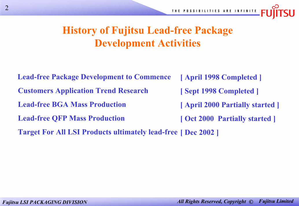
2
History of Fujitsu Lead-free PackageDevelopment Activities
Lead-free Package Development to Commence
Customers Application Trend Research
Lead-free BGA Mass Production
Lead-free QFP Mass Production
Target For All LSI Products ultimately lead-free
[ April 1998 Completed ]
[ Sept 1998 Completed ]
[ April 2000 Partially started ]
[ Oct 2000 Partially started ]
[ Dec 2002 ]
Fujitsu LSI PACKAGING DIVISION ©All Rights Reserved, Copyright Fujitsu Limited
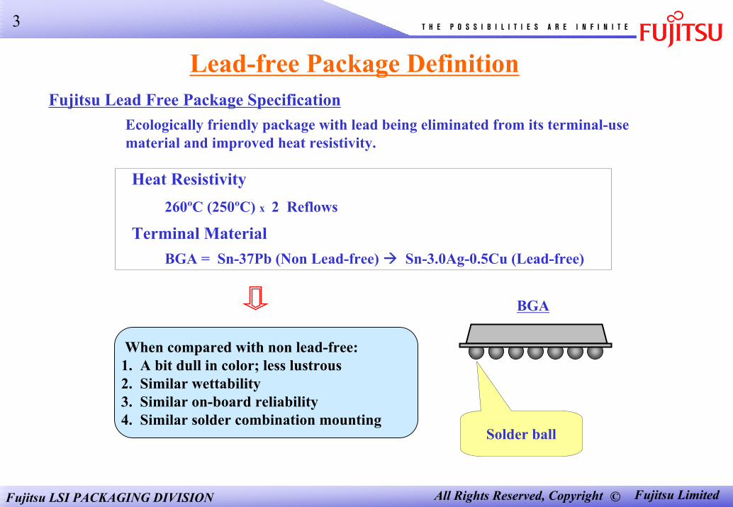
3
Lead-free Package DefinitionFujitsu Lead Free Package Specification
Ecologically friendly package with lead being eliminated from its terminal-usematerial and improved heat resistivity.
Heat Resistivity260ºC (250ºC) x 2 Reflows
Terminal MaterialBGA = Sn-37Pb (Non Lead-free) Sn-3.0Ag-0.5Cu (Lead-free)
BGA
Solder ball
When compared with non lead-free:1. A bit dull in color; less lustrous 2. Similar wettability 3. Similar on-board reliability4. Similar solder combination mounting
Fujitsu LSI PACKAGING DIVISION ©All Rights Reserved, Copyright Fujitsu Limited
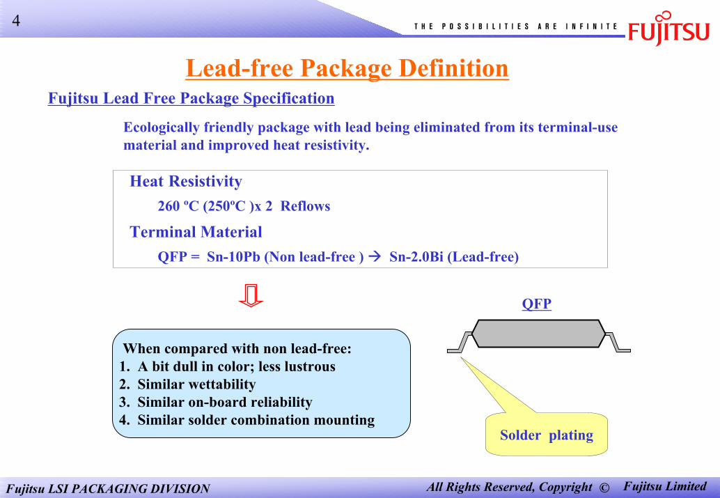
4
Lead-free Package DefinitionFujitsu Lead Free Package Specification
Ecologically friendly package with lead being eliminated from its terminal-usematerial and improved heat resistivity.
Heat Resistivity260 ºC (250ºC )x 2 Reflows
Terminal MaterialQFP = Sn-10Pb (Non lead-free ) Sn-2.0Bi (Lead-free)
QFP
Solder plating
When compared with non lead-free:1. A bit dull in color; less lustrous 2. Similar wettability 3. Similar on-board reliability4. Similar solder combination mounting
Fujitsu LSI PACKAGING DIVISION ©All Rights Reserved, Copyright Fujitsu Limited
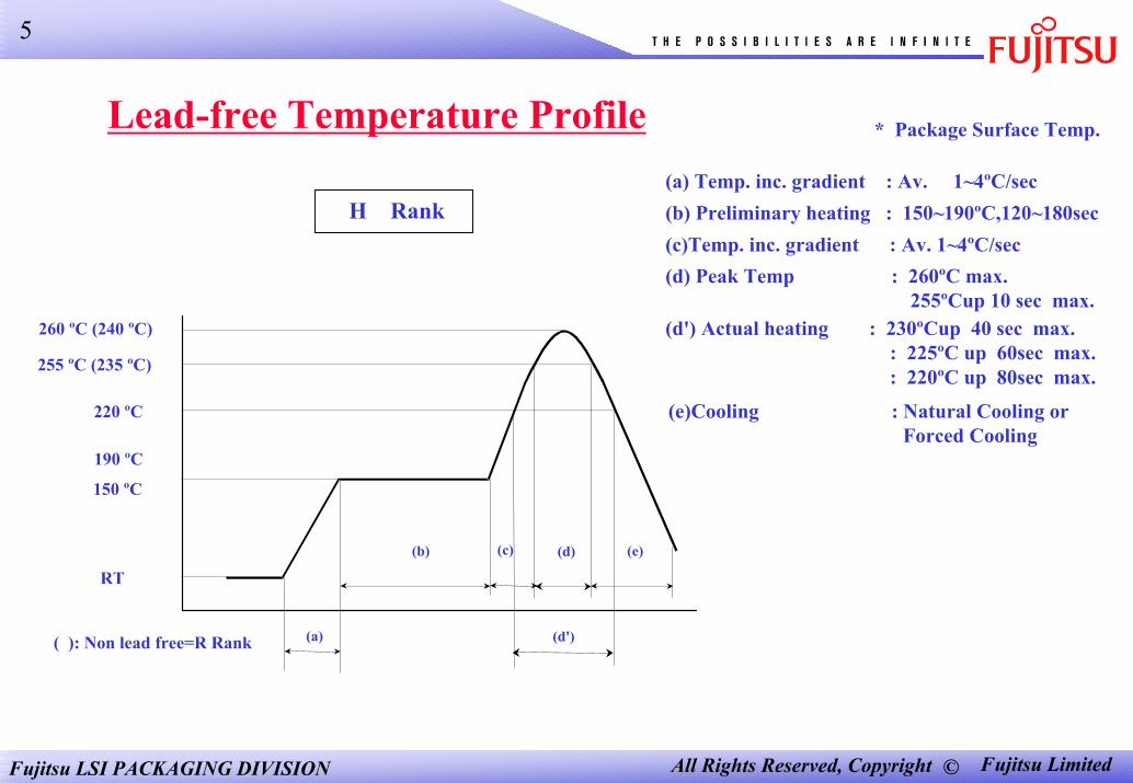
5
Lead-free Temperature Profile * Package Surface Temp.
(a) Temp. inc. gradient : Av. 1~4ºC/secH Rank (b) Preliminary heating : 150~190ºC,120~180sec
(c)Temp. inc. gradient : Av. 1~4ºC/sec(d) Peak Temp : 260ºC max.
255ºCup 10 sec max.(d') Actual heating : 230ºCup 40 sec max.
: 225ºC up 60sec max.: 220ºC up 80sec max.
(e)Cooling : Natural Cooling or Forced Cooling
(a) (d')
(b) (e)(d)(c)
260 ºC (240 ºC)
255 ºC (235 ºC)
220 ºC
150 ºC
190 ºC
RT
( ): Non lead free=R Rank
Fujitsu LSI PACKAGING DIVISION ©All Rights Reserved, Copyright Fujitsu Limited
6
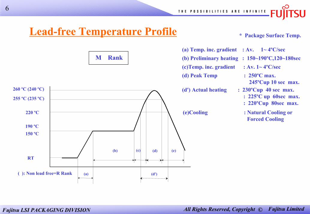
Lead-free Temperature Profile * Package Surface Temp.
(a) Temp. inc. gradient : Av. 1~ 4ºC/secM Rank (b) Preliminary heating : 150~190ºC,120~180sec
(c)Temp. inc. gradient : Av. 1~ 4ºC/sec(d) Peak Temp : 250ºC max.
245ºCup 10 sec max.260 ºC (240 ºC) (d') Actual heating : 230ºCup 40 sec max.
: 225ºC up 60sec max.: 220ºCup 80sec max.
(e)Cooling : Natural Cooling or Forced Cooling
(a) (d')
(b) (e)(d)(c)
255 ºC (235 ºC)
220 ºC
150 ºC190 ºC
RT
( ): Non lead free=R Rank
Fujitsu LSI PACKAGING DIVISION ©All Rights Reserved, Copyright Fujitsu Limited
7
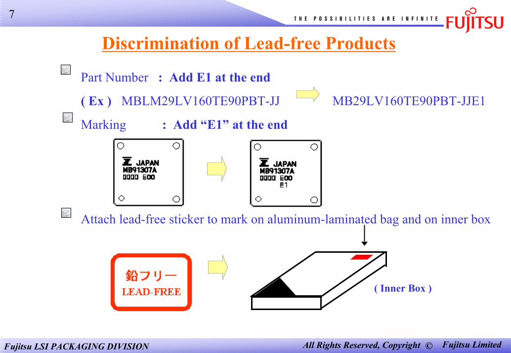
Discrimination of Lead-free Products
Part Number : Add E1 at the end
( Ex ) MBLM29LV160TE90PBT-JJ MB29LV160TE90PBT-JJE1
Marking : Add “E1” at the end
Attach lead-free sticker to mark on aluminum-laminated bag and on inner box
( Inner Box )
Fujitsu LSI PACKAGING DIVISION ©All Rights Reserved, Copyright Fujitsu Limited
8
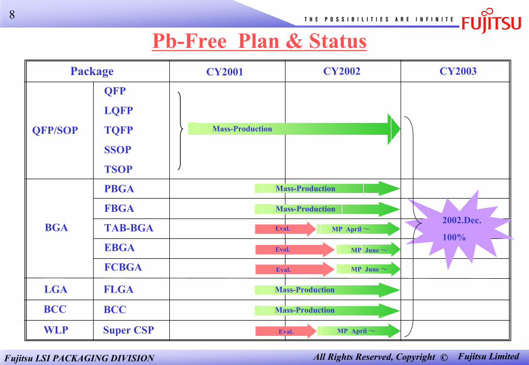
Pb-Free Plan & StatusPackage
QFP/SOP
QFP
LQFP
TQFP
SSOP
TSOP
BGA
PBGA
FBGA
TAB-BGA
EBGA
FCBGA
LGA FLGA
BCC BCC
WLP Super CSP
Eval.
Mass-Production
MP April ~2002.Dec.
100%
Mass-Production
Mass-Production
Mass-Production
Mass-Production
Eval.
Eval.
Eval. MP April ~
MP June ~
MP June ~
CY2001 CY2002 CY2003
Fujitsu LSI PACKAGING DIVISION ©All Rights Reserved, Copyright Fujitsu Limited
9
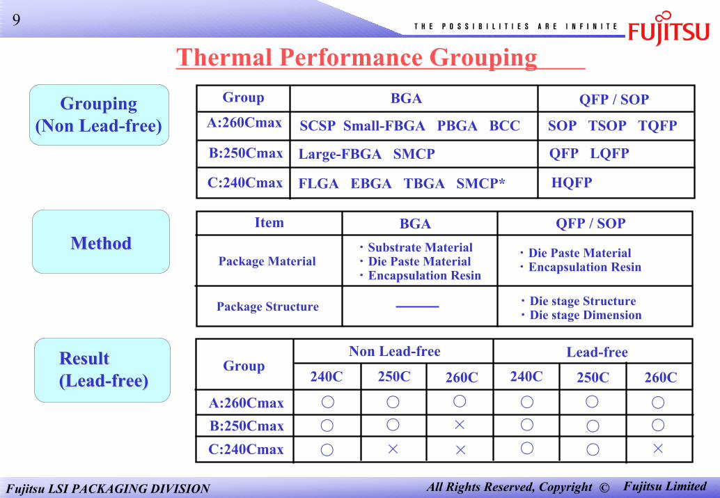
Thermal Performance Grouping
BGA
SCSP Small-FBGA PBGA BCC
FLGA EBGA TBGA SMCP*
Large-FBGA SMCP
QFP / SOP
SOP TSOP TQFP
HQFP
QFP LQFP
Group
A:260Cmax
B:250Cmax
C:240Cmax
Grouping(Non Lead-free)
Package Material
Package Structure
・Substrate Material・Die Paste Material・Encapsulation Resin
Item BGA
・Die stage Structure・Die stage Dimension
QFP / SOP
・Die Paste Material・Encapsulation Resin
MethodMethod
Non Lead-free Lead-free
〇
×
×
〇
〇
〇
〇
〇 〇
〇
〇
〇
〇
〇
〇
〇
×
Group
×
A:260CmaxB:250CmaxC:240Cmax
240C 250C 260C 240C 250C 260CResultResult(Lead(Lead--free)free)
Fujitsu LSI PACKAGING DIVISION ©All Rights Reserved, Copyright Fujitsu Limited
10
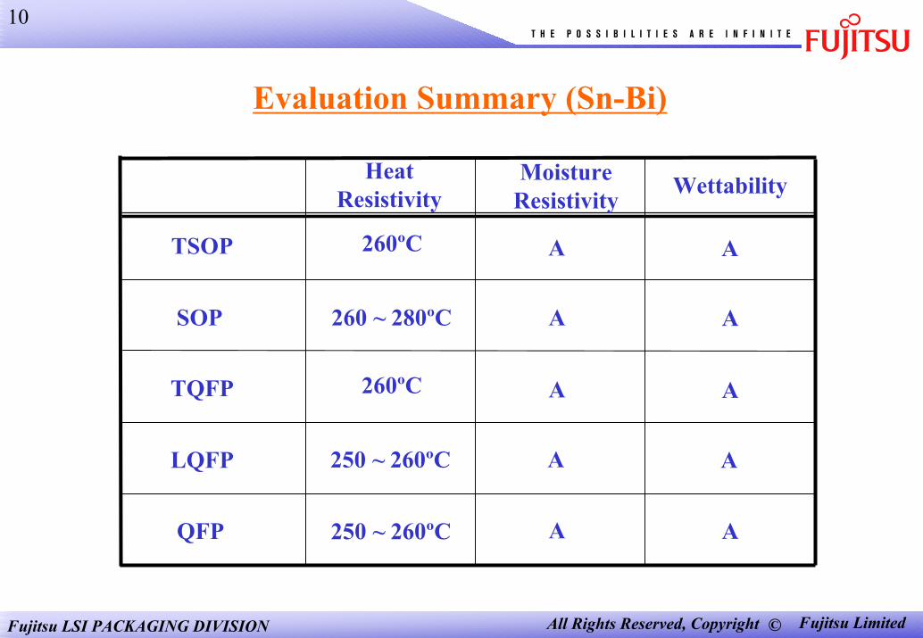
Evaluation Summary (Sn-Bi)
MoistureResistivity WettabilityHeat
Resistivity
260ºCTSOP A
A
A
A
A
A
A
A
A
A
SOP 260 ~ 280ºC
260ºCTQFP
250 ~ 260ºCLQFP
QFP 250 ~ 260ºC

Fujitsu LSI PACKAGING DIVISION ©All Rights Reserved, Copyright Fujitsu Limited
11
DisadvantageComposition Advantage
BGA Ball Evaluaion
Sn-Ag-Cu
Sn-Ag-Bi-Cu
High Melting Point (220ºC)
Lower Mounting Reliability byBi content increase
Better Mounting Reliability than Sn-Pb/Sn-Pb
Lower Melting point than Sn-Ag-Cu
Ball share Strength
Shar
e St
reng
thgF)
1000
0H
Package:FBGA224(0.8mmP)Ball Diameter.:φ0.5mm
Aging : 125ºC Storage
・・・Sn-Ag-Cu
・・・Sn-Ag-Bi-Cu
・・・Sn-Pb168H 336H 504H 1000H
Fujitsu LSI PACKAGING DIVISION ©All Rights Reserved, Copyright Fujitsu Limited
12
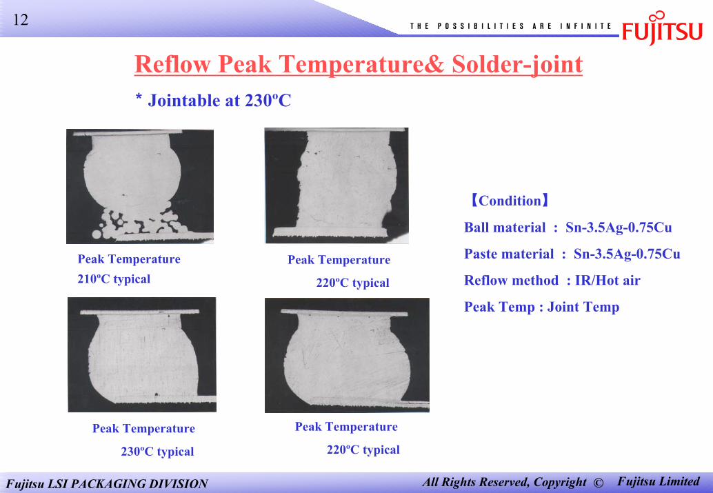
Reflow Peak Temperature& Solder-joint*Jointable at 230ºC
【Condition】
Ball material : Sn-3.5Ag-0.75Cu
Paste material : Sn-3.5Ag-0.75Cu
Reflow method : IR/Hot air
Peak Temp : Joint Temp
Peak Temperature210ºC typical
Peak Temperature
220ºC typical
Peak Temperature
220ºC typical
Peak Temperature
230ºC typical
Fujitsu LSI PACKAGING DIVISION ©All Rights Reserved, Copyright Fujitsu Limited
13
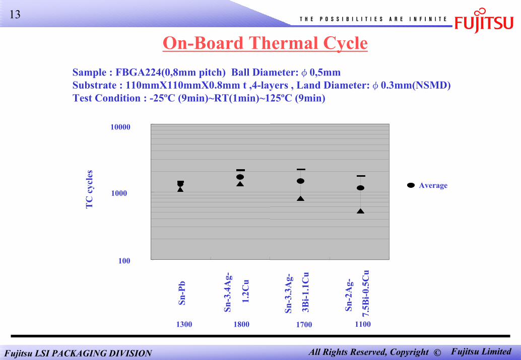
On-Board Thermal CycleSample : FBGA224(0,8mm pitch) Ball Diameter:φ0,5mm Substrate : 110mmX110mmX0.8mm t ,4-layers , Land Diameter:φ0.3mm(NSMD)Test Condition : -25ºC (9min)~RT(1min)~125ºC (9min)
10000
TC
cyc
les
Average1000
100
Sn-P
b
Sn-3
.4A
g-
1.2C
u
Sn-3
.3A
g-
3Bi-1
.1C
u
Sn-2
Ag-
7.5B
i-0.5
Cu
1300 1800 1700 1100
Fujitsu LSI PACKAGING DIVISION ©All Rights Reserved, Copyright Fujitsu Limited
14
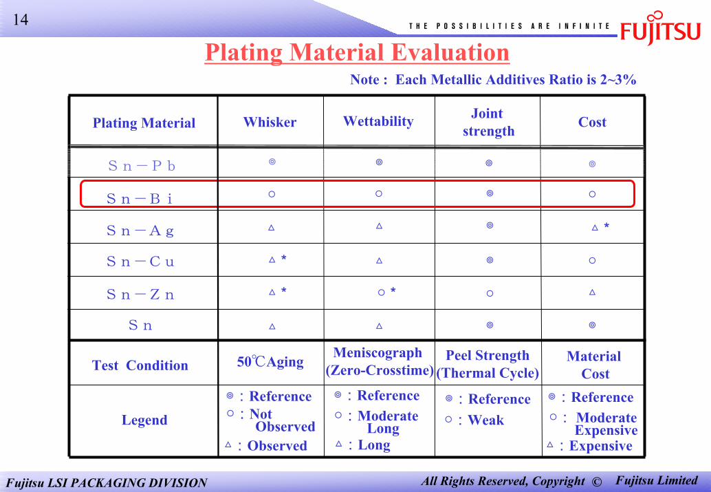
Note : Each Metallic Additives Ratio is 2~3%Plating Material Evaluation
△:Expensive
◎
○
◎
○
Sn-Pb
Sn-Bi
○:Not Observed
△:Observed
Legend ○: Moderate Expensive
Material Cost
◎:Reference
◎
○
◎:Reference○:Moderate
Long△:Long
◎:Reference○:Weak
Meniscograph(Zero-Crosstime)
Peel Strength(Thermal Cycle)
◎
◎
◎
◎
◎
○○*
Jointstrength
Wettability CostWhiskerPlating Material
△ △*△Sn-Ag
△* ○△Sn-Cu
△△*Sn-Zn
◎△△Sn
50℃AgingTest Condition
◎:Reference

Fujitsu LSI PACKAGING DIVISION ©All Rights Reserved, Copyright Fujitsu Limited
15
Zero-Cross TimeSample Size : 3.30xo.46xo.25t Dipping Speed :10mm/sec Dipping Depth : 1mm
Test Condition-1Solder : Sn-Ag-Bi-CuSolder Temperature : 230ºCFlux : RA type
Test Condition-2Solder : Sn-Ag--CuSolder Temperature : 230ºCFlux : RA type
Test Condition-3Solder : Sn-Pb(Reference)Solder Temperature : 220ºCFlux : RA type
0
1
2
3
4
5
0h 24h 48h 72h 96h
170℃エー シ ン゙グ
セロ゙クロスタイム(sec)
S n-Bi/42材 Sn-Bi/C u材Sn-Pb/42材 Sn-Pb/C u材
0
1
2
3
4
5
0h 1h 2h 4h 6h 8h
ス チー ム エー シ ン゙グ
セロ゙クロスタイム(sec)
2Bi/42材 2Bi/C u材10Pb/42材 10Pb/C u材
0
1
2
3
4
5
0h 24h 48h 72h 96h
170℃エー シ ン゙グ
セロ゙クロスタイム(sec)
S n-Bi/42材 Sn-Bi/42材Sn-Pb/42材 Sn-Pb/C u材
0
1
2
3
4
5
0h 1h 2h 4h 6h 8h
ス チー ム エー シ ン゙グ
セロ゙クロスタイム(sec)
2Bi/42材 2Bi/C u材10Pb/42材 10Pb/C u材
0
1
2
3
4
5
0h 24h 48h 72h 96h
170℃エー シ ン゙グ
セロ゙クロスタイム(sec)
S n-Bi/42材 Sn-Bi/C u材Sn-Pb/42材 Sn-Pb/C u材
0
1
2
3
4
5
0h 1h 2h 4h 6h 8h
ス チー ム エー シ ン゙グ
セロ゙クロスタイム(sec)
2Bi/42材 2Bi/C u材10Pb/42材 10Pb/C u材
Fujitsu LSI PACKAGING DIVISION ©All Rights Reserved, Copyright Fujitsu Limited
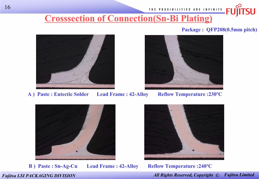
16
Crosssection of Connection(Sn-Bi Plating)Package : QFP208(0.5mm pitch)
A ) Paste : Eutectic Solder Lead Frame : 42-Alloy Reflow Temperature :230ºC
B ) Paste : Sn-Ag-Cu Lead Frame : 42-Alloy Reflow Temperature :240ºC

Fujitsu LSI PACKAGING DIVISION ©All Rights Reserved, Copyright Fujitsu Limited
17
Example of Lead-free Whisker
Sample A : Sn-Cu (42Alloy) Sample A : Sn-Cu (42Alloy)
Sample A: Sn-Cu (42Alloy) Sample B: Sn-Ag (42Alloy)
Fujitsu LSI PACKAGING DIVISION ©All Rights Reserved, Copyright Fujitsu Limited
18
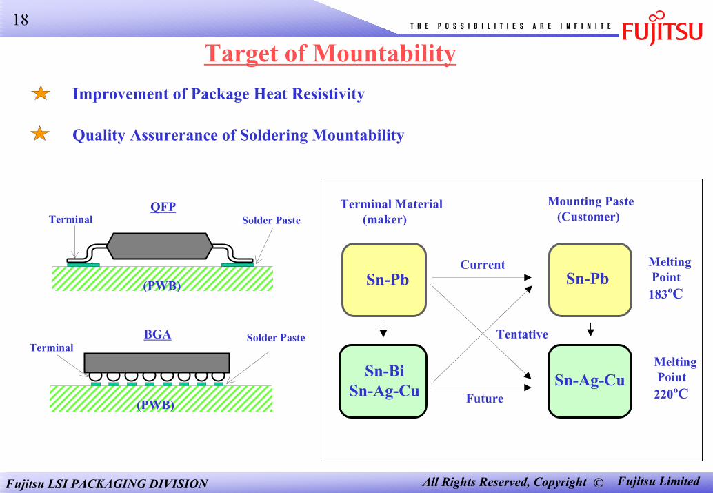
Target of MountabilityImprovement of Package Heat Resistivity
Quality Assurerance of Soldering Mountability
Sn-Pb Sn-Pb
Sn-BiSn-Ag-Cu Sn-Ag-Cu
Terminal Material(maker)
Mounting Paste(Customer)
Current
Future
MeltingPoint183ºC
MeltingPoint220ºC
Tentative
QFPTerminal
(PWB)
Solder Paste
BGATerminal
Solder Paste
(PWB)
Fujitsu LSI PACKAGING DIVISION ©All Rights Reserved, Copyright Fujitsu Limited
19
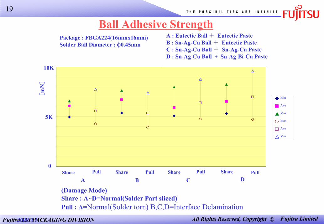
Ball Adhesive Strength[
mN]
10K
Min
Ave
Max
Max
Ave
Min
PullShare Share Share SharePull Pull PullA B C D
5K
0
A : Eutectic Ball + Eutectic PasteB : Sn-Ag-Cu Ball + Eutectic PasteC : Sn-Ag-Cu Ball + Sn-Ag-Cu PasteD : Sn-Ag-Cu Ball + Sn-Ag-Bi-Cu Paste
Package : FBGA224(16mmx16mm)Solder Ball Diameter : φ0.45mm
(Damage Mode) Share : A~D=Normal(Solder Part sliced)Pull : A=Normal(Solder torn) B,C,D=Interface Delamination
2000.9.1
Fujitsu LSI PACKAGING DIVISION ©All Rights Reserved, Copyright Fujitsu Limited
20
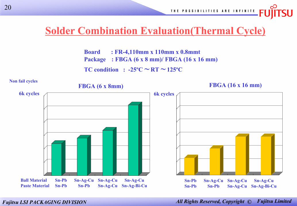
Solder Combination Evaluation(Thermal Cycle)
Board : FR-4,110mm x 110mm x 0.8mmtPackage : FBGA (6 x 8 mm)/ FBGA (16 x 16 mm)
TC condition : -25ºC ~ RT ~ 125ºC
FBGA (6 x 8mm)
Sn-PbSn-Pb
Sn-Ag-CuSn-Pb
Sn-Ag-CuSn-Ag-Cu
Sn-Ag-CuSn-Ag-Bi-Cu
Ball MaterialPaste Material
FBGA (16 x 16 mm)
Sn-PbSn-Pb
Sn-Ag-CuSn-Pb
Sn-Ag-CuSn-Ag-Cu
Sn-Ag-CuSn-Ag-Bi-Cu
6k cycles
Non fail cycles
6k cycles
Fujitsu LSI PACKAGING DIVISION ©All Rights Reserved, Copyright Fujitsu Limited
21
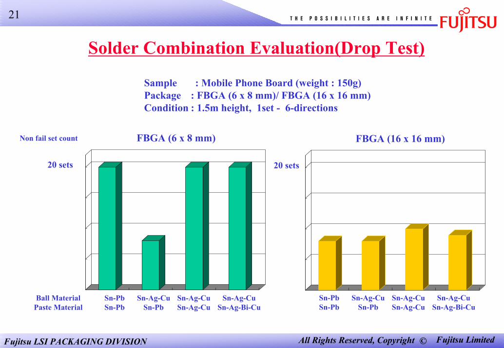
Solder Combination Evaluation(Drop Test)
Sample : Mobile Phone Board (weight : 150g)Package : FBGA (6 x 8 mm)/ FBGA (16 x 16 mm)Condition : 1.5m height, 1set - 6-directions
FBGA (16 x 16 mm)
Sn-PbSn-Pb
Sn-Ag-CuSn-Pb
Sn-Ag-CuSn-Ag-Cu
Sn-Ag-CuSn-Ag-Bi-Cu
FBGA (6 x 8 mm)
Sn-PbSn-Pb
Sn-Ag-CuSn-Pb
Sn-Ag-CuSn-Ag-Cu
Sn-Ag-CuSn-Ag-Bi-Cu
Ball Material Paste Material
20 sets
Non fail set count
20 sets
Fujitsu LSI PACKAGING DIVISION ©All Rights Reserved, Copyright Fujitsu Limited
22
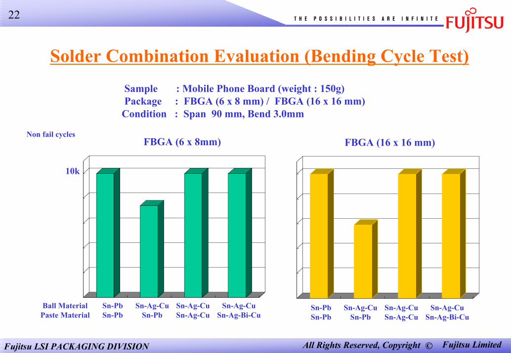
Solder Combination Evaluation (Bending Cycle Test)Sample : Mobile Phone Board (weight : 150g)Package : FBGA (6 x 8 mm) / FBGA (16 x 16 mm)
Condition : Span 90 mm, Bend 3.0mm
Non fail cyclesFBGA (6 x 8mm)
Sn-PbSn-Pb
Sn-Ag-CuSn-Pb
Sn-Ag-CuSn-Ag-Cu
Sn-Ag-CuSn-Ag-Bi-Cu
FBGA (16 x 16 mm)
Sn-PbSn-Pb
Sn-Ag-CuSn-Pb
Sn-Ag-CuSn-Ag-Cu
Sn-Ag-CuSn-Ag-Bi-Cu
Ball MaterialPaste Material
10k
Fujitsu LSI PACKAGING DIVISION ©All Rights Reserved, Copyright Fujitsu Limited
23
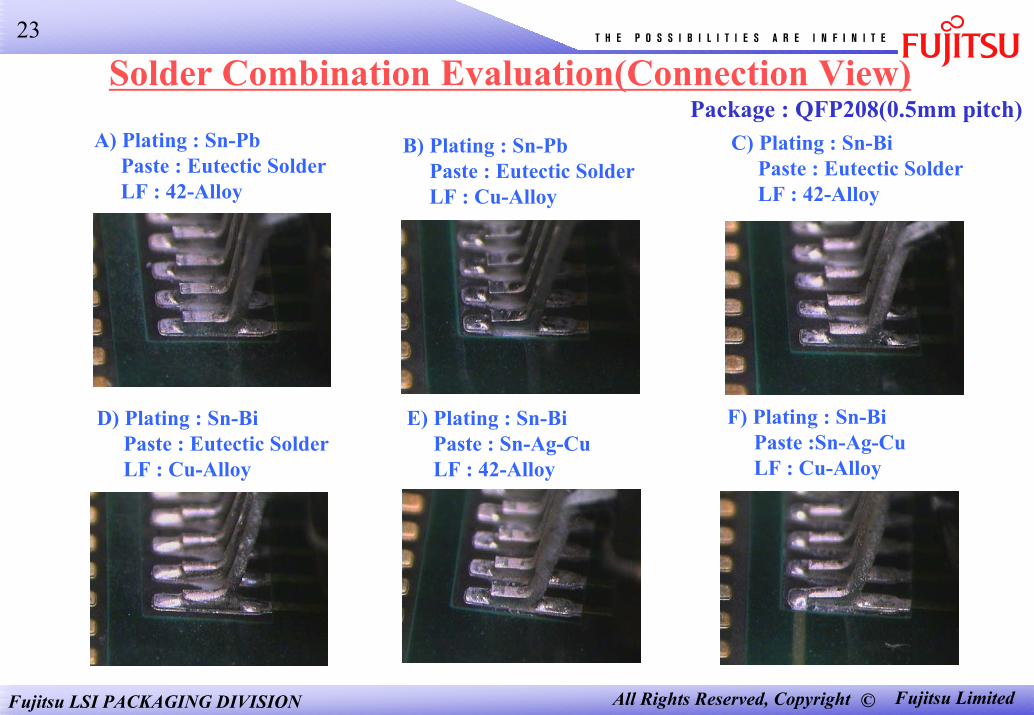
Solder Combination Evaluation(Connection View)Package : QFP208(0.5mm pitch)
A) Plating : Sn-Pb Paste : Eutectic SolderLF : 42-Alloy
C) Plating : Sn-Bi Paste : Eutectic SolderLF : 42-Alloy
B) Plating : Sn-Pb Paste : Eutectic SolderLF : Cu-Alloy
F) Plating : Sn-Bi Paste :Sn-Ag-CuLF : Cu-Alloy
D) Plating : Sn-Bi Paste : Eutectic SolderLF : Cu-Alloy
E) Plating : Sn-Bi Paste : Sn-Ag-CuLF : 42-Alloy
Fujitsu LSI PACKAGING DIVISION ©All Rights Reserved, Copyright Fujitsu Limited
24
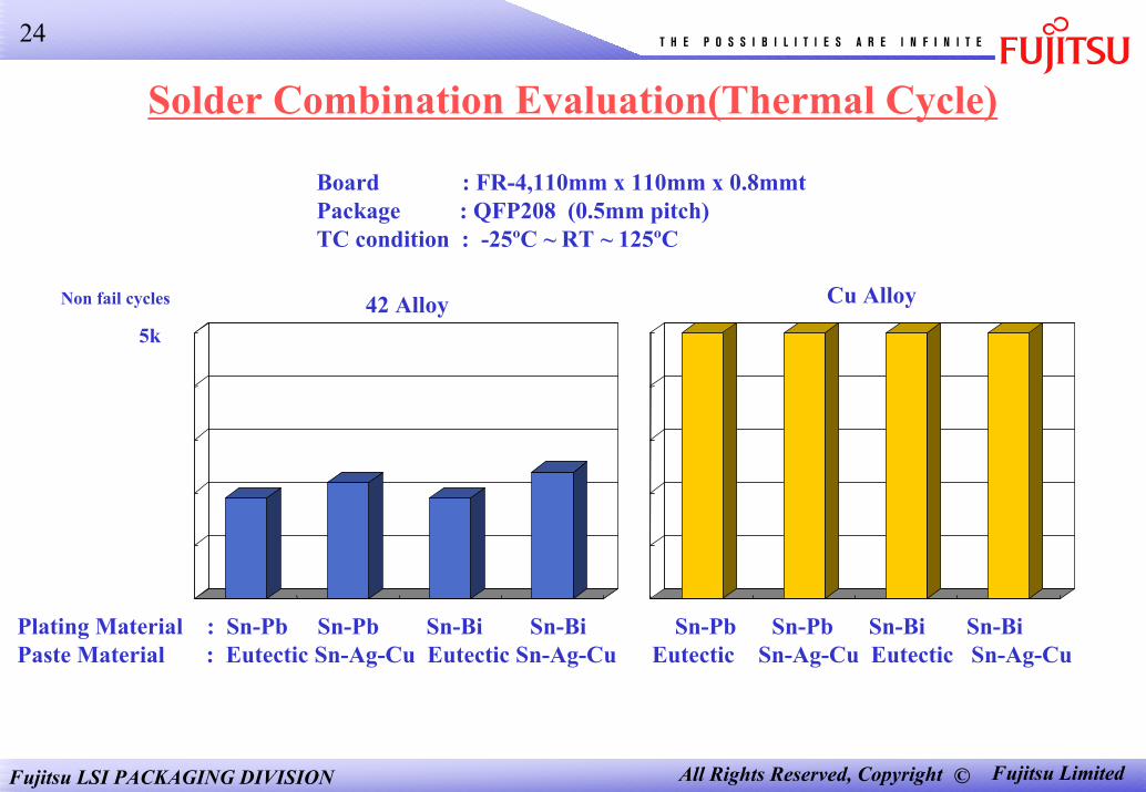
Solder Combination Evaluation(Thermal Cycle)
Board : FR-4,110mm x 110mm x 0.8mmtPackage : QFP208 (0.5mm pitch)TC condition : -25ºC ~ RT ~ 125ºC
Cu AlloyNon fail cycles 42 Alloy5k
Plating Material : Sn-Pb Sn-Pb Sn-Bi Sn-Bi Sn-Pb Sn-Pb Sn-Bi Sn-BiPaste Material : Eutectic Sn-Ag-Cu Eutectic Sn-Ag-Cu Eutectic Sn-Ag-Cu Eutectic Sn-Ag-Cu
Fujitsu LSI PACKAGING DIVISION ©All Rights Reserved, Copyright Fujitsu Limited
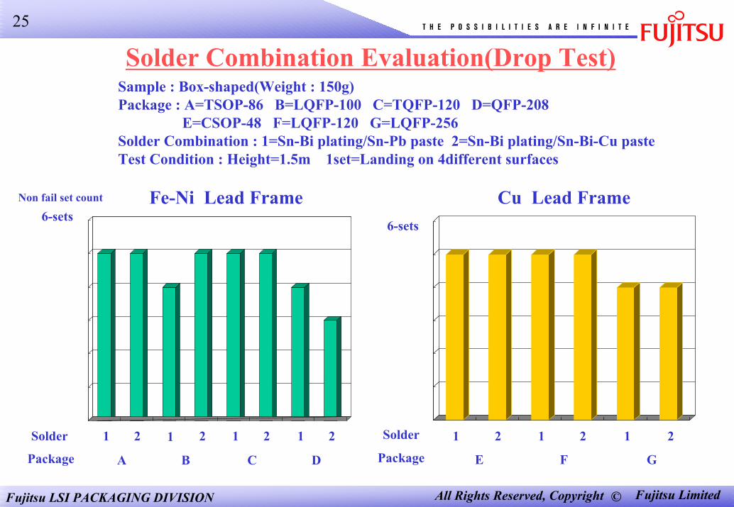
25
Solder Combination Evaluation(Drop Test)Sample : Box-shaped(Weight : 150g)Package : A=TSOP-86 B=LQFP-100 C=TQFP-120 D=QFP-208
E=CSOP-48 F=LQFP-120 G=LQFP-256Solder Combination : 1=Sn-Bi plating/Sn-Pb paste 2=Sn-Bi plating/Sn-Bi-Cu pasteTest Condition : Height=1.5m 1set=Landing on 4different surfaces
Cu Lead Frame
Solder
Package E F G
1 1 12 2 2
Non fail set count Fe-Ni Lead Frame
Solder
Package A B C D
1 1 1 12 2 2 2
6-sets6-sets
Fujitsu LSI PACKAGING DIVISION ©All Rights Reserved, Copyright Fujitsu Limited
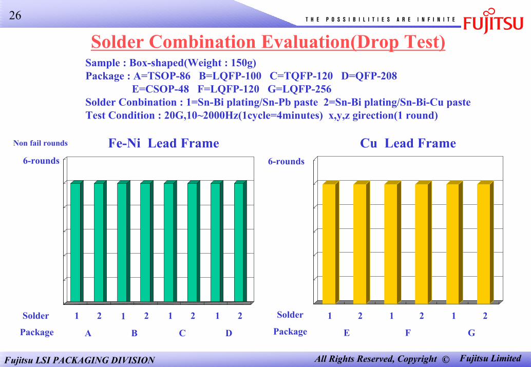
26
Solder Combination Evaluation(Drop Test)Sample : Box-shaped(Weight : 150g)Package : A=TSOP-86 B=LQFP-100 C=TQFP-120 D=QFP-208
E=CSOP-48 F=LQFP-120 G=LQFP-256Solder Conbination : 1=Sn-Bi plating/Sn-Pb paste 2=Sn-Bi plating/Sn-Bi-Cu pasteTest Condition : 20G,10~2000Hz(1cycle=4minutes) x,y,z girection(1 round)
Fe-Ni Lead Frame6-rounds
Solder
Package A B C D
1 1 1 12 2 2 2
Cu Lead Frame6-rounds
Solder
Package E F G
1 1 12 2 2
Non fail rounds
Fujitsu LSI PACKAGING DIVISION ©All Rights Reserved, Copyright Fujitsu Limited
27
Conclusion of Fujitsu Lead-free Package
1. Heat resistivity = 260ºC (250ºC)x 2 Reflows2. Terminal materials
BGA = Sn-Ag-Cu (Ball)QFP = Sn-Bi (Plating)
3. Discrimination of products by:Parts number, marking, Lead-Free Sticker
4. Solder combinations work just as well with non lead-free version
5. Completed by Dec 2002 (Target)