fully printed separated carbon nanotube thin film transistor circuits 2 and its application in...
DESCRIPTION
Pochiang Chen,†,|| Yue Fu,‡,|| Radnoosh Aminirad,†,§ Chuan Wang,‡ Jialu Zhang,‡ Kang Wang,§4 Kosmas Galatsis,*,†,§ and Chongwu Zhou*,‡TRANSCRIPT
1 Fully Printed Separated CarbonNanotube Thin Film Transistor Circuits2 and Its Application in Organic Light Emitting Diode Control3 Pochiang Chen,†,|| Yue Fu,‡,|| Radnoosh Aminirad,†,§ Chuan Wang,‡ Jialu Zhang,‡ Kang Wang,§
4 Kosmas Galatsis,*,†,§ and Chongwu Zhou*,‡
5†Aneeve Nanotechnologies LLC, 570 Westwood Plaza, Suite 6532, Los Angeles, California 90095, United States
6‡Department of Electrical Engineering, University of Southern California, Los Angeles, California 90089, United States
7§Department of Electrical Engineering, University of California at Los Angeles, Los Angeles, California 90095, United States
8 bS Supporting Information
24 Since the revolutionary inventions of liquid crystal displays25 (LCDs) in 1964,1,2 display electronics has undergone rapid26 developments and has attracted growing attention. Recently, the27 organic light emitting diode (OLED)3 has shed new light on this28 realm. Compared to LCD, OLED has lightweight, compatibility29 with flexible plastic substrate, wide viewing angles, improved30 brightness, high power efficiency, and quick response. OLED-31 based displays are now used in cell phones, digital cameras and32 other portable devices. An OLED-based flexible and rollable33 display prototype has also been demonstrated.4 To allow low-34 cost, mass production of OLED-based displays, key issues include35 the materials and processes used for fabrication of OLED and36 controlling the circuit. A commercial LED/OLED-based display37 adopts polysilicon TFT or amorphous silicon (α-Si) TFT for38 compatibility with the mainstream silicon fabrication process.39 However, deposition of amorphous silicon and polysilicon re-40 quires a complex high-cost fabrication process. Among possible41 solutions, printing technology has great potential. It is a simple,42 low-cost, high throughput process and has been used for many43 electronic applications.5�12 Plus, it is compatible with flexible44 substrates, making it suitable for manufacturing of OLED-based45 displays. While polysilicon and amorphous silicon are not com-46 patible with printing, some organic semiconductors can be47 printed, but they suffer from low mobility and instability in air.48 In contrast, single-walled carbon nanotubes (SWCNTs) are49 well-known for their high mobility, high on/off ratio, and small50 operation voltage.13�15 They have been used for sensors16�19
51and digital circuits such as ring oscillators,21�24 simple logic gates52(inverters, NOR, NAND),20�24 decoders,20 SRAM22 and delay53flip flops (DFFs).24 Due to the excellent current carrying capacity54of SWCNTs, SWCNT TFT can provide sufficient driving55current for typical high-resolution OLED displays than organic56TFTs. Such advantages allow dense integration of pixels, high57aperture ratio, and small power consumption. Furthermore,58carbon nanotubes (CNTs) are flexible materials, and their59solution is compatible with printed electronics.60The advantages of SWCNT TFTs for active matrix OLED61(AMOLED) display electronics have been previously demon-62strated.25,26 However, no one has reported using SWCNT TFTs63based on printing technology for display applications. In this64study, we have demonstrated the first circuits composed of fully65printed back-gated and top-gated SWCNT TFTs for display66electronics. Our work includes the following essential compo-67nents: (1) We fabricated back-gated SWCNT TFTs with high68mobility (10�30 cm2/(V s)) and high on/off ratio (104�107)69purely based on printing technology. (2) With printed poly-70ethylenimine (PEI)/LiClO4 as polymer electrolyte gating ma-71terial, we fabricated fully printed top-gated SWCNT TFTs with72good current carrying capability. (3) We demonstrated the first73fully printed single pixel OLED control circuits. Our fully printed
Received: August 10, 2011Revised: October 17, 2011
9 ABSTRACT: The advantages of printed electronics and semi-10 conducting single-walled carbon nanotubes (SWCNTs) are11 combined for the first time for display electronics. Conductive12 silver ink and 98% semiconductive SWCNT solutions are used13 to print back-gated thin film transistors with high mobility, high14 on/off ratio, and high current carrying capacity. In addition,15 with printed polyethylenimine with LiClO4 as the gating16 material, fully printed top-gated devices have been made to17 work as excellent current switches for organic light emitting18 diodes (OLEDs). An OLED driving circuit composed of two19 top-gated fully printed transistors has been fabricated, and the successful control over external OLED is demonstrated. Our work20 demonstrates the significant potential of using printed carbon nanotube electronics for display backplane applications.
21 KEYWORDS: Separated semiconducting-enriched carbon nanotubes, printed electronics, display electronics, organic light22 emitting diode, fully printed carbon nanotube devices and circuits, thin film transistors
23
Nano Letters | 3b2 | ver.9 | 4/11/011 | 20:43 | Msc: nl-2011-02765b | TEID: rlt00 | BATID: 00000 | Pages: 7.12
LETTER
pubs.acs.org/NanoLett
rXXXX American Chemical Society A dx.doi.org/10.1021/nl202765b |Nano Lett. XXXX, XXX, 000–000

74 SWCNT TFTs and circuits show significant advantage over75 traditional organic-based printed electronics with respect to76 stability and device performance. It suggests a practical approach77 for a printable, flexible OLED display and other SWCNT-based78 printed electronics.79 Panels a and b of Figure 1F1 show the schematic diagrams of two80 typical control circuits for OLED displays, one with a single81 transistor and a storage capacitor (1T1C),27 and the other with82 two transistors and one storage capacitor (2T1C).28 These two83 circuit structures have been printed in this work without the84 storage capacitor and was tested with an external OLED with the85 structure shown in Figure 1c. Figure 1d shows the process of86 printing of both back-gated and top-gated SWCNT TFTs on a87 Si/SiO2 wafer. Briefly, a commercial silver nanoparticle solution88 (Cabot Corp., CCI 300) is first printed to form source and drain89 electrodes, as well as gate pads to be used later for top-gated TFT90 structures. A postprinting sintering of the silver electrodes at91 180 �Cwas performed to achieve small resistance (∼1Ω/sq), as92 was measured by the Van Der Pauw method. To improve the93 adhesion of SWCNT to Si/SiO2 wafers, wafers are functionalized94 by diluted (aminopropyl)triethoxysilane (APTES) following our95 previously published recipe,25 before printing of 98% semicon-96 ductive SWCNT solution (NanoIntegris Inc.) as the active97 channel material. Then the devices were rinsed with deionized98 (DI) water to remove the sodium dodecyl sulfate (SDS) residue99 after the printed SWCNT solution dried out. After inspection of100 the CNT film to confirm the uniformity and desired CNT101 density using a field emission scanning electron microscope102 (FESEM), another layer of silver electrodes was added along103 the border of silver and SWCNT film, to improve the contact104 between silver electrodes and SWCNT networks. Electric
105measurements were performed to inspect the performance of106these SWCNT TFTs before printing of polymer electrolyte.107Finally, PEI/LiClO4 is printed as the top gate dielectric as well as108gate electrode, expanding from the gate pad to the SWCNT film109in the channel.110Uniformity and high density of the printed CNT film are two111important issues for the printed back-gated TFTs. Panels a�c of112Figure 2 F2show details of the as-printed back-gated SWCNT113TFTs, especially for the channel region, including an optical114image (Figure 2a) showing a 3-in. wafer with back-gated115SWCNT TFTs with various channel widths (W) and channel116lengths (L), followed by FESEM images (Figure 2b) showing the117uniformity of CNT network in the channel region. A further118zoomed-in FESEM image (Figure 2c) shows an approximate119CNT density of 24�32 tubes/μm2, which is comparable to that120of previously reported SWCNT TFT work.25,29
121Electric characterization was carried out for the as-fabricated122back-gated devices. The channel width of the devices we studied123ranges approximately from 100 to 500 μm, while the channel124length ranges from 10 to 200 μm. More accurate values of the W125and L used in mobility derivation are all measured via FESEM.126Most devices exhibit an on-state current (Ion) of 1�10 μA at127drain voltage of 1.0 V and gate voltage of �20 V, on/off ratio of128104�107, mobility of 10�30 cm2/(V s), and Vth of �5.0 V.129Panels d�f of Figure 2 show the electric characteristics of one130representative device with W = 510.5 μm and L = 88.8 μm.131Figure 2g shows the plot of drain current (ISD) versus gate132voltage (VG) (green curve), and the plot of divided transcon-133ductance versus VG (blue curve). The IDS�VDS family curves134display a clear linear regime (Figure 2e), indicating Ohmic135contacts formed between the silver electrodes and CNT
Figure 1. Schematic diagrams of typical display control circuits, OLED structure, and fabrication process of fully printed top-gated SWCNT TFT. (a)Schematic diagram of the 1T1C display control circuit. (b) Schematic diagram of the 2T1C display control circuit. (c) Cross-section view of an OLEDstructure. (d) Schematic diagram illustrating the fully printed back-gated and top-gated SWCNT TFT fabrication process.
Nano Letters LETTER
B dx.doi.org/10.1021/nl202765b |Nano Lett. XXXX, XXX, 000–000

136 networks. Pronounced saturation behavior is observed when VD137 becomes more negative, as is shown in Figure 2d. The ISD�VG
138 curves measured in the linear regime (Figure 2f) show Ion of139 9.0 μA at VSD = 0.8 V and VG = �20 V, corresponding to a140 current density of 0.037 μA/μm. On/off ratio of the device is141 estimated to be 1.28 � 107.142 We have calculated the mobility following
μ ¼ LW
1CoxVSD
dISDdVG
143 where L andW are the device channel length and width, VSD = 1 V,144 the ISD�VG curve is measured at VSD = 1 V, and Cox is the gate145 capacitance per unit area. If we treat the nanotube film as a146 uniform and continuous film, we can use a simple parallel model147 to calculate Cox
Cox ¼ ε0εoxtox
¼ 6:90� 10�9 F=cm2
148 given that the dielectric is 500 nm SiO2. This results in a mobility149 of 23.1 cm2/(V s). If we consider the quantum capacitance of the150 nanotube network, there is a more sophisticated and rigorous151 model30 to calculate Cox, which gives
Cox ¼ D1CQl
þ 12πε0εox
lnsinhð2πtoxDÞ
πRD
� �
152 where CQl = 4 � 10�10 F/m is the quantum capacitance of a153 single nanotube30 andD≈ 28 tubes/μm is the nanotube density.154 This gives Cox = 6.74 � 10�9 F/cm2, which is similar to the Cox
155 value based on the parallel-plate model. This is expected as the156 capacitance generated by 500 nm of SiO2 is much smaller than157 the quantum capacitance generated by the nanotube network.158 Since these two capacitances are in series, the smaller one should159 dominate. Hence we adopted the simple model for mobility160 calculation of all back-gated SWCNT TFTs.161 More information can be found in Figure S2a�c in the162 Supporting Information about mobility, Ion and on/off ratio163 versusW and L. This study shows that these back-gated devices164 have relatively uniform device performance, and tunable Ion by165 designing properW and L without compromise of mobility and166 on/off ratio. Overall, these as-printed SWCNT TFT devices167 show similar performance to their photolithography-made168 SWCNT TFT counterparts.25,29
169 On the basis of the measured high Ion, high on/off ratio, as well170 as highmobility of the printed SWCNTTFTs, we further explore171 their application in display electronics. For proof of concept, we172 connected an OLED to a typical SWCNT TFT back-gated173 device. The connection is made by putting a probe onto the174 drain electrode of the device, and the probe is connected to a175 clamp by a coaxial cable. The clamp is then fixed on the anode of176 the OLED. The cathode of the OLED is clamped and connected177 to the ground by another coaxial cable. The schematic diagram of178 this testing circuit is plotted in the insets of panels h and I of179 Figure 2. Both the device performance (ISD�VG and IDS�VDS180 family curves) and the OLED characterization can be found in181 Figure S1a-d in the Supporting Information. The OLED struc-182 ture used in this study is a 4,40-bis[N-(1-naphthyl)-N-phenyla-183 mino]biphenyl (NPD)/tris(8-hydroxyquinoline)aluminum184 (Alq3) green light OLED with indium tin oxide (ITO) as the185 anode and aluminum (Al) as the cathode. Figure 2f shows a186 family of OLED current (IOLED) versus VG curves. A close
187inspection of the curve measured at VSS = �10 V and VG =188�10 V reveals that the current flowing through the OLED is 21.4189μA; when VG = 10 V, the current flowing through the OLED is190378.0 pA. This corresponds to a modulation of IOLED of 5.7 �191104. From the IOLED�VSS curves shown in Figure 2i, good diode192behavior is observed with a clear cutoff region and triode region193under different VG, showing good control from the SWCNT194TFT over the OLED. The cutoff voltage of VSS is around�3.5 V,195in accordance with the threshold voltage of the OLED.196From the figures, the SWCNT TFT was able to provide197enough driving current (21.4 μA when VG = �10 V and VSS =198�10 V) for OLED, which requires around 1 μA to have199observable light emission. The optical images in Figure 2j show200the OLED of different light intensity under different VG values of201control SWCNT TFT, at fixed VSS = �10 V. From the optical
Figure 2. Characterization of fully printed back-gated SWCNT TFTsand their OLED control capability. (a�c) Optical and SEM images offully printed back-gated SWCNT TFTs. (d, e) Output (IDS�VDS)characteristics of a representative device in saturation regime (d) andtriode regime (e), respectively. (f) Transfer (ISD�VG) characteristics ofthe same device. (g) ISD�VG curve (green) of the same device measuredat VSD = 1.0 V and its corresponding gm�VG curve (blue). (h, i) Electricmeasurement of back-gated TFT connected to an external OLED, insetshows the circuit diagram, including IOLED�VG curves (f) andIOLED�VSS curves (g). (j) Optical images showing OLED light intensitymodulation through VG of back-gated SWCNT TFT at VSS = �10 V,photos numbered from 1 to 5 correspond to OLED under VG = �10,�6, �2, 2, and 6 V, respectively. Inset shows the circuit diagram.
Nano Letters LETTER
C dx.doi.org/10.1021/nl202765b |Nano Lett. XXXX, XXX, 000–000

202 images, the OLED is very bright whenVG = 10 V, gets dimmed as203 VG increases positively, and is totally turned off when VG204 becomes more positive (6 V), corresponding to the IOLED�VG
205 curve measured at VSS = �10 V in Figure 2h, where the curve206 enters the cutoff region around 5.5 V.207 This single transistor used in the above OLED control test can208 be viewed as a modified control circuit shown in Figure 1a. The209 next step is to realize the more complicated display control circuit210 shown in Figure 1b, which allows longer storage time than the211 circuit in Figure 1a. The easiest way is to fabricate top gate212 SWCNT TFTs based on the back-gated TFTs we have printed.213 Here we used PEI (Mw: 10k, Sigma Aldrich) as ion gel dielectric214 for SWCNT TFTs. Due to the large molecular weight, pure PEI215 has a high viscosity and therefore is unable to print out. Here we216 dissolve PEI in methanol in 1:5 volume ratio, and then stir for217 overnight to reduce the viscosity before printing. Besides, to218 improve the gate conductance, a small amount of LiClO4
219 (LiClO4 to PEI weight ratio: 1�2.5) is added to fine-tune the220 device performance. Figure 3F3 a shows the optical images of arrays of221 top-gated SWCNT TFTs, a top-gated SWCNT TFT, and a222 zoomed-in image of the channel region, respectively. The fully223 printed top-gated SWCNT TFTs were characterized by electric224 measurement in ambient air. Interestingly, ambipolar behavior was225 observed for most devices. Panels b and c of Figure 3 show the226 ISD�VG and ISD�VSD curves of a typical ambipolar device. This is227 different from what was reported in the literature,31�34 where228 n-type SWCNT transistors were obtained when pure PEI or PEI/
229LiClO4 was spin coated to cover the whole device and used as the230ion gel dielectric. Here we notice that the coverage of our fully231printed SWCNT TFT is different from literature, and it may232explainwhat we observed. From the optical image in Figure 3a, only233part of the channel is covered with PEI/LiClO4 and part of the234channel is exposed to air, while in literature,31�34 the channel235region of CNT devices is fully covered with spin-coated PEI/236LiClO4. SWCNT TFTs are p-type in ambient air because the237oxygen molecules adsorbed onto nanotubes can act as electron238acceptors. However, it has been reported that the carrier type in239SWCNTs can be modified by introducing electron donors or240acceptors. PEI/LiClO4 is known to change the carrier type of CNT241from p-type to n-type, because the oxygen atom in PEI/LiClO4 can242be adsorbed onto the SWNT sidewall and act as electron donors to243compensate for the p-type doping effect from the oxygen mol-244ecules. If the PEI/LiClO4 coverage is 100%, then thewhole channel245region would become n-type, and the devices would assume246exclusively n-type behavior. However, if only the middle part of247the channel region is covered by PEI/LiClO4, then only the middle248part of the channel becomes n-type doped while the uncovered249regions still remain p-type. Such a doping condition may induce250band-to-band (BTB) tunneling35 under certain biasing conditions251while operating as aMOSFET under some other biasing condition,252showing ambipolar behavior in ISD�VG curves.We also notice that253the coverage of PEI/LiClO4 needs to be beyond a certain point to254reduce the tunneling distance so as to favor BTB tunneling or the255device would become very resistive after PEI printing.
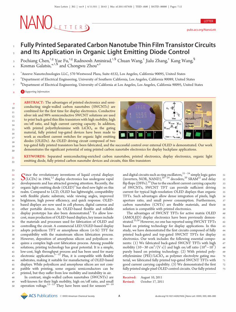
Figure 3. Characterization of fully printed top-gated SWCNTTFTs on a Si/SiO2 wafer. (a)Optical images of fully printed top-gated SWCNTTFTs ona Si/SiO2 wafer. (b, c) Transfer (ISD�VG) characteristics of one typical top-gated SWCNT TFT on a Si/SiO2 wafer, showing ambipolar behavior. (c)Output (IDS�VDS) characteristics of the same device. (d�f) Energy band diagram of top-gated SWCNT TFTs operating in p-type branch (d), deadzone (e), and n-type branch (f).
Nano Letters LETTER
D dx.doi.org/10.1021/nl202765b |Nano Lett. XXXX, XXX, 000–000
256 Such carrier type modulation via the coverage of PEI/LiClO4
257 of these fully printed top-gated devices could be more clearly258 explained by the energy band diagrams. Figure 3d�f shows the259 energy band structure of p-type conduction, a dead zone with260 little conduction, and n-type conduction due to BTB tunneling.261 The green arrows denote which type of carrier is favored. When262 VG is negative, both the ungated and gated nanotube sections are263 p-type, and holes can flow from source to drain, therefore leading264 to p-type conduction (Figure 3d). As VG increases positively, the265 gated nanotube would become gradually n-type, while the266 ungated nanotubes remain p-type, resulting in the nonconduc-267 tive dead zone (Figure 3e). However, as VG becomes even more268 positive, the tunneling barrier between the p-type region and the269 n-type region becomes very thin, thereby favoring BTB tunneling270 current (Figure 3f).271 Besides conduction mechanism, other important electrical272 characteristics are subthreshold slope and mobility. From273 Figure 3b, the subthreshold swings of an ambipolar top-gated274 device are calculated to be 258 mV/decade for p-type branch and275 136 mV/decade for n-type branch. Mobility calculation for a276 polymer-gated device requires more analysis of total gate capa-277 citance. From ref 33, the capacitance provided by PEI/LiClO4
278 polymer should be
CPG ¼ εε0λ
279 where λ is the Debye length calculated by
λ ¼ffiffiffiffiffiffiffiffiffiffiffiffiεε0kT2Fe2
s
280 Here, F is the concentration of LiClO4, ε = 10 is the dielectric281 constant of PEI. The calculated value for CPG is 2.062 � 10�3
282 F/cm2. Quantum capacitance generated by a carbon nanotube
283network is quantified by
CQ ¼ CQlD ¼ 1:12� 10�6 F=cm2
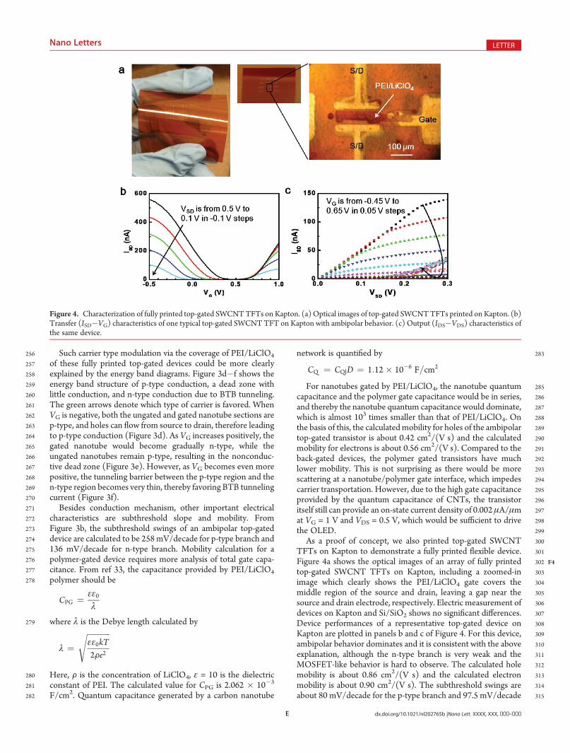
284285For nanotubes gated by PEI/LiClO4, the nanotube quantum286capacitance and the polymer gate capacitance would be in series,287and thereby the nanotube quantum capacitance would dominate,288which is almost 103 times smaller than that of PEI/LiClO4. On289the basis of this, the calculatedmobility for holes of the ambipolar290top-gated transistor is about 0.42 cm2/(V s) and the calculated291mobility for electrons is about 0.56 cm2/(V s). Compared to the292back-gated devices, the polymer gated transistors have much293lower mobility. This is not surprising as there would be more294scattering at a nanotube/polymer gate interface, which impedes295carrier transportation. However, due to the high gate capacitance296provided by the quantum capacitance of CNTs, the transistor297itself still can provide an on-state current density of 0.002μA/μm298at VG = 1 V and VDS = 0.5 V, which would be sufficient to drive299the OLED.300As a proof of concept, we also printed top-gated SWCNT301TFTs on Kapton to demonstrate a fully printed flexible device.302Figure 4 F4a shows the optical images of an array of fully printed303top-gated SWCNT TFTs on Kapton, including a zoomed-in304image which clearly shows the PEI/LiClO4 gate covers the305middle region of the source and drain, leaving a gap near the306source and drain electrode, respectively. Electric measurement of307devices on Kapton and Si/SiO2 shows no significant differences.308Device performances of a representative top-gated device on309Kapton are plotted in panels b and c of Figure 4. For this device,310ambipolar behavior dominates and it is consistent with the above311explanation, although the n-type branch is very weak and the312MOSFET-like behavior is hard to observe. The calculated hole313mobility is about 0.86 cm2/(V s) and the calculated electron314mobility is about 0.90 cm2/(V s). The subthreshold swings are315about 80 mV/decade for the p-type branch and 97.5 mV/decade
Figure 4. Characterization of fully printed top-gated SWCNTTFTs on Kapton. (a) Optical images of top-gated SWCNTTFTs printed on Kapton. (b)Transfer (ISD�VG) characteristics of one typical top-gated SWCNTTFT on Kapton with ambipolar behavior. (c) Output (IDS�VDS) characteristics ofthe same device.
Nano Letters LETTER
E dx.doi.org/10.1021/nl202765b |Nano Lett. XXXX, XXX, 000–000

316 for the n-type branch. The on-state current density is about317 0.001 μA/μm.318 We have also compared the hysteresis of all the devices319 mentioned above: back-gated devices on silicon wafers, top-320 gated ambipolar devices on Kapton, and top-gated ambipolar321 devices on Si/SiO2 wafers. This piece of information can be322 found in Figure S3a�c in Supporting Information. Hysteresis of323 top-gated devices is very small, compared to that of the back-324 gated devices, probably due to stronger gating effect offered by325 the top gate. We demonstrated a simple inverter function by326 using two fully printed top-gated transistors. Additional informa-327 tion can be found in Figure 4 in the Supporting Information.328 Stability is an important issue in commercialization of any useful329 technology. For AMOLED applications, we envision that the330 printed carbon nanotube transistors will be fully integrated with331 OLED arrays, and the encapsulation technology developed for332 OLEDs will also keep the CNT transistors well protected, as the333 organics in OLEDs are very sensitive to oxygen and moisture.334 Thereby OLEDs, instead of CNT transistors, would set the335 lifetime of the AMOLED display. Regarding printed CNT tran-336 sistors without encapsulation, while CNTs and silver electrodes337 are stable in air, a typical lifetime of PEI/LiClO4 in air is reported
338to be at least several weeks.33 As mentioned above, proper339encapsulation can mitigate and eliminate the stability problem.340Study of how the PEI/LiClO4 operates as gate dielectric for341SWCNTTFTs paves the way for 2T1COLED control circuit. For342demonstration purpose, we omitted the storage capacitance and343tested the transistor-only (2T) OLED control circuit. The photo-344graph of the fully printed 2T OLED display circuit is shown in345Figure 5 F5a, and the inset shows the equivalent schematic circuit346diagram of this as-fabricated circuit. The atomic force microscopy347(AFM) image shown in Figure 5b is taken before PEI/LiClO4
348printing, confirming that the carbon nanotube density of this349device is very high. Electric property characterizations were done350first without the OLED, as indicated in the circuit diagram shown351in the inset of Figure 5d.WithVDD biased at 0.1 , 0.2 , 0.3 , 0.4, and3520.5 V andVData swept from�1 to 1 V, whenVScan = 0V, the switch353transistor is cut off and there is no current through the driving354transistor.WhenVScan =�0.5 V, the switch transistor turns on and355it passes VData to the driving transistor. The details of how VData356controls the current provided by the driving transistor (IDD) are357plotted in Figure 5d, under differentVDD ranging from0.5 to 0.1 V.358Specifically, the IDD�VData curve measured under VDD = 0.3 V is359magnified and replotted in Figure 5e, in both linear and log scales.
Figure 5. Characterization of the 2T control circuit made of two fully printed top-gated SWCNT TFTs. (a) Optical image of one 2T OLED displaycontrol circuit, inset shows corresponding circuit diagram. (b) AFM image of channel region of the transistors in 2TOLED display control circuit beforePEI/LiClO4 printing. (c) Optical images taken at VData =�1.0 V (1),�0.5 V (2), and 0.2 V (3), respectively. VDD is 0.3 V and VScan is �0.5 V. (d, e)Characterization of 2T control circuit alone, including IDD�VData curves (d), and one IDD�VData curve in both linear plot (green) and log plot (blue)(e).( f) IDD�VData curves of 2T control circuit connected to external OLED.
Nano Letters LETTER
F dx.doi.org/10.1021/nl202765b |Nano Lett. XXXX, XXX, 000–000

360 Subsequently, an external OLED is directly connected to this361 display circuit, with the cathode connected to the drain of the362 driving transistor and anode connected to a negative voltage of363 �3.4 V, which is used to provide the voltage drop onOLED in on364 state. The connections aremade via probes and coaxial cables with365 clamps in a way similar to connecting an external OLED to a366 single device, which has been described. IDD�VData wasmeasured367 atVDD= 0.1, 0.2, 0.3, 0.4, and 0.5 V (Figure 5f).Modulation of the368 OLED light output can be clearly observed, and the optical images369 in Figure 5c numbered 1, 2, 3 were taken under VData = �1.0,370 �0.5, and 0.2 V, respectively, when VDD = �0.3 V.371 In addition, we carried out frequency investigation of single372 top-gated and back-gated transistors. This study is included in373 Figure S5a�d in Supporting Information. The 3 dB frequency is374 found to be 5.66 kHz for back-gated SWCNT TFT and 93.3 Hz375 for top-gated SWCNT TFT.376 In summary, we have successfully fabricated fully printed377 SWCNT TFT circuits for OLED control and display. The378 back-gated printed transistors are made of 98% semiconducting379 SWCNTs as the channel and printed Ag nanoparticles as380 electrodes, and they exhibit good mobility (10�30 cm2/381 (V s)), good on/off ratio (104�107), and good current carrying382 capacity. They are ideal components for OLED-based display383 backplane electronics, and the control over external OLED using384 one single back-gated SWCNT TFT is demonstrated. In addi-385 tion, with one more printing step of PEI/LiClO4, these back-386 gated SWCNT TFTs are converted to top-gated SWCNT TFTs387 with ambipolar behavior. Furthermore, top-gated SWCNT388 TFTs are also made on Kapton to demonstrate the potential of389 using this technology for flexible electronics. Finally, a two-390 transistor OLED control circuit composed of two fully printed391 top-gated SWCNT TFTs is made and its ability to control over392 external OLED is demonstrated. Our work shows the great393 potential of printed electronics based on semiconducting carbon394 nanotubes as a cost-effective and scalable approach for display395 backplane electronics (OLED and LCD) and other macroelec-396 tronics applications.
397 ’ASSOCIATED CONTENT
398 bS Supporting Information. Electric properties of the exter-399 nal OLED and the control device used in Figure 2 (S1), statistic400 study of Ion, mobilities, and on/off ratio of the fully printed back-401 gated SWCNTTFTs (S2), hysteresis of the fully printed back-gated402 and top-gated devices (S3), electric properties of the inverter403 composed of two top-gated devices (S4), and frequency study of404 the fully printed back-gated and top-gateddevices (S5). Thismaterial405 is available free of charge via the Internet at http://pubs.acs.org.
406 ’AUTHOR INFORMATION
407 Corresponding Author408 *E-mail: [email protected], [email protected].
409 Author Contributions410
)These authors contributed equally to this work.
411 ’ACKNOWLEDGMENT
412 We acknowledge financial support by a DARPA SBIR Con-413 tract (HR 0011-10-0-0003) and Defense Threat Reduction414 Agency (HDTRA1-10-1-0015). We thank Dr. Todd Hylton
415from the Defense Science Office of DARPAR for helpful416suggestions. We thank Professor Mark Hersam of Northwestern417University and Mr. Elliott Garlock and Dr. Nathan Yoder of418Nanointegris for valuable discussions.
419’REFERENCES
420(1) Heilmeie, G. H.; Castella, J. A.; Zanoni, L. A. Mol. Cryst. Liq.421Cryst. 1969, 8, 293–304.422(2) Heilmeie, G. H.; Zanoni, L. A.; Barton, L. A. Pr. Inst. Electr. Elect.4231968, 56, 1162–1171.424(3) Tang, C. W.; Vanslyke, S. A. Appl. Phys. Lett. 1987, 51, 913–915.425(4) Nusca, Andrew Amazing: Sony’s paper-thin ’rollable’ flexible426OLED display. ZDNet (May 26, 2010). Retrieved July 26, 2011 from427http://www.zdnet.com/blog/gadgetreviews/amazing-sonys-paper-428thin-rollable-flexible-oled-display/15136.429(5) Rogers, J. A.; Bao, Z.; Baldwin, K.; Dodabalapur, A.; Crone, B.;430Raju, V. R.; Kuck, V.; Katz, H.; Amundson, K.; Ewing, J.; Drzaic, P. Proc.431Natl. Acad. Sci. U.S.A. 2001, 98, 4835–4840.432(6) Bao, Z. N.; Feng, Y.; Dodabalapur, A.; Raju, V. R.; Lovinger, A.433J. Chem. Mater. 1997, 9, 1299–&.434(7) Liu, Y.; Cui, T. H.Macromol. Rapid Commun. 2005, 26, 289–292.435(8) Cho, J. H.; Lee, J.; Xia, Y.; Kim, B.; He, Y. Y.; Renn, M. J.; Lodge,436T. P.; Frisbie, C. D. Nat. Mater. 2008, 7, 900–906.437(9) Liu, Y.; Cui, T. H.; Varahramyan, K. Solid-State Electron. 2003,43847, 1543–1548.439(10) Chen, B.; Cui, T. H.; Liu, Y.; Varahramyan, K. Solid-State440Electron. 2003, 47, 841–847.441(11) Liu, Y.; Varahramyan, K.; Cui, T. H.Macromol. Rapid Commun.4422005, 26, 1955–1959.443(12) Rogers, J. A.; Bao, Z. N.; Dodabalapur, A.; Makhija, A. IEEE444Electron Device Lett. 2000, 21, 100–103.445(13) Javey, A.; Guo, J.; Wang, Q.; Lundstrom, M.; Dai, H. J. Nature4462003, 424, 654–657.447(14) Durkop, T.; Getty, S. A.; Cobas, E.; Fuhrer, M. S. Nano Lett.4482004, 4, 35–39.449(15) Kang, S. J.; Kocabas, C.; Ozel, T.; Shim, M.; Pimparkar, N.;450Alam, M. A.; Rotkin, S. V.; Rogers, J. A. Nat. Nanotechnol. 2007,4512, 230–236.452(16) Kong, J.; Franklin, N. R.; Zhou, C.; Chapline, M. G.; Peng, S.;453Cho, K.; Dai, H. Science 2000, 287, 622.454(17) Ishikawa, F. N.; Curreli, M.; Olson, C. A.; Liao, H.-I.; Sun, R.;455Roberts, R. W.; Cote, R. J.; Thompson, M. E.; Zhou, C. ACS Nano 2010,4564, 6914–6922.457(18) Ishikawa, F. N.; Stauffer, B.; Caron, D. A.; Zhou, C. Biosens.458Bioelectron. 2009, 24, 2967–2972.459(19) Barone, P. W.; Baik, S.; Heller, D. A.; Strano, M. S. Nat. Mater.4602005, 4, 86–92.461(20) Cao, Q.; Kim, H. S.; Pimparkar, N.; Kulkarni, J. P.; Wang, C. J.;462Shim,M.; Roy, K.; Alam,M. A.; Rogers, J. A.Nature 2008, 454, 495–500.463(21) Javey, A.; Wang, Q.; Ural, A.; Li, Y. M.; Dai, H. J. Nano Lett.4642002, 2, 929–932.465(22) Bachtold, A.; Hadley, P.; Nakanishi, T.; Dekker, C. Science4662001, 294, 1317–1320.467(23) Chen, Z. H.; Appenzeller, J.; Lin, Y. M.; Sippel-Oakley, J.;468Rinzler, A. G.; Tang, J. Y.; Wind, S. J.; Solomon, P.M.; Avouris, P. Science4692006, 311, 1735–1735.470(24) Sun, D.-m.; Timmermans, M. Y.; Tian, Y.; Nasibulin, A. G.;471Kauppinen, E. I.; Kishimoto, S.; Mizutani, T.; Ohno, Y. Nat. Nanotech-472nol. 2011, 6, 156–161.473(25) Wang, C.; Zhang, J. L.; Ryu, K.M.; Badmaev, A.; De Arco, L. G.;474Zhou, C. W. Nano Lett. 2009, 9, 4285–4291.475(26) Ishikawa, F. N.; Chang, H. K.; Ryu, K.; Chen, P. C.; Badmaev,476A.; De Arco, L. G.; Shen, G. Z.; Zhou, C. W. ACS Nano 2009, 3, 73–79.477(27) Tsukada, T. TFT/LCD Liquid-Crystal Displays Addressed by478Thin-Film Transistors; Gordon and Breach Publishers: Austrailia, 1994;479Vol. 29, p 193.
Nano Letters LETTER
G dx.doi.org/10.1021/nl202765b |Nano Lett. XXXX, XXX, 000–000

480 (28) Chen, P. C.; Shen, G. Z.; Chen, H. T.; Ha, Y. G.; Wu, C.;481 Sukcharoenchoke, S.; Fu, Y.; Liu, J.; Facchetti, A.; Marks, T. J.; Thomp-482 son, M. E.; Zhou, C. W. ACS Nano 2009, 3, 3383–3390.483 (29) Wang, C.; Zhang, J. L.; Zhou, C. W. ACS Nano 2010, 4,484 7123–7132.485 (30) Cao, Q.; Xia, M. G.; Kocabas, C.; Shim, M.; Rogers, J. A. Appl.486 Phys. Lett. 2007, 90, 023516.487 (31) Shim, M.; Javey, A.; Kam, N. W. S.; Dai, H. J. J. Am. Chem. Soc.488 2001, 123, 11512–11513.489 (32) Lu, C. G.; Fu, Q.; Huang, S. M.; Liu, J. Nano Lett. 2004,490 4, 623–627.491 (33) Siddons, G. P.; Merchin, D.; Back, J. H.; Jeong, J. K.; Shim, M.492 Nano Lett. 2004, 4, 927–931.493 (34) Ozel, T.; Gaur, A.; Rogers, J. A.; Shim, M. Nano Lett. 2005, 5,494 905–911.495 (35) Appenzeller, J.; Lin, Y. M.; Knoch, J.; Avouris, Ph. Phys. Rev.496 Lett. 2004, 93, 196805.
Nano Letters LETTER
H dx.doi.org/10.1021/nl202765b |Nano Lett. XXXX, XXX, 000–000