functional materials programme greetings from the … mh 10-2011. ... orion, juhani luotola, ... sun...
TRANSCRIPT
Copyright © Tekes
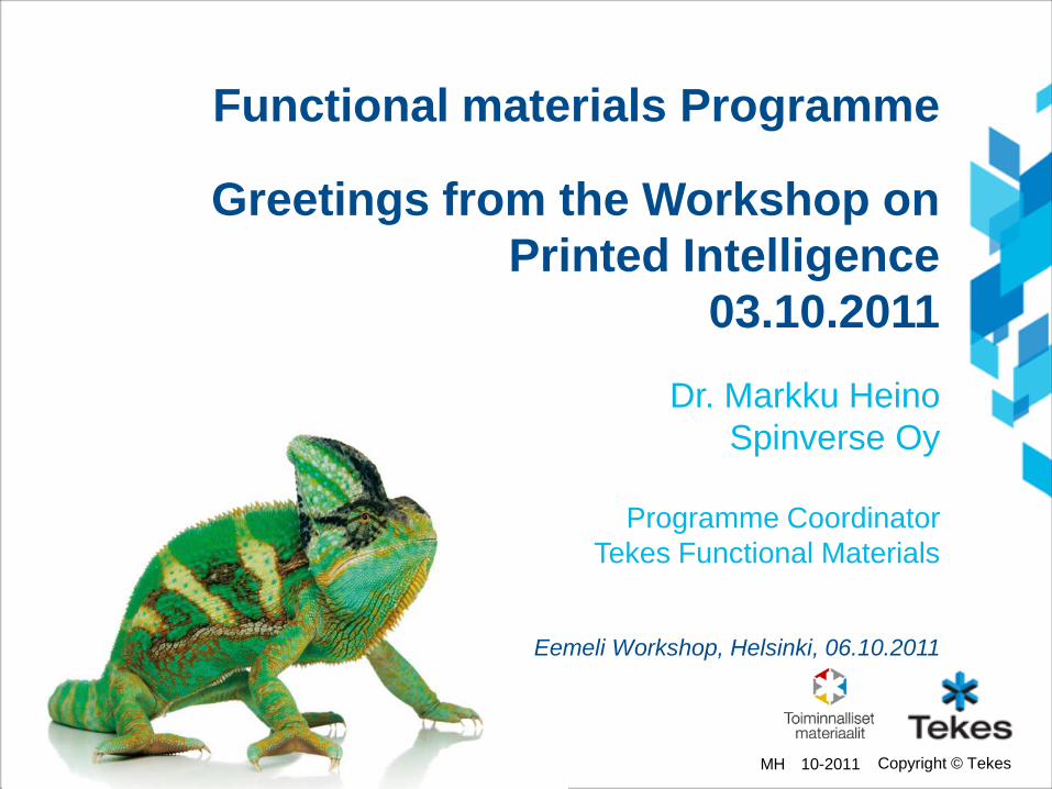
Functional materials Programme
Greetings from the Workshop on
Printed Intelligence
03.10.2011
Dr. Markku Heino
Spinverse Oy
Programme Coordinator
Tekes Functional Materials
Eemeli Workshop, Helsinki, 06.10.2011
10-2011MH

Copyright © Tekes
Overview Functional Materials Programme 2007-2013
Programme includes
Over 100 companies and all
relevant Finnish research
organizations
International collaboration with
40 countries, in the top Germany,
Japan, Sweden, UK and USA
Programme volume:
ca. 205 M EUR, of which
Tekes accounts for 84 M EUR
Project portfolio as of 18.5.2011
46 research projects
45 company projects
We aim to develop new applications and
competive advantage through materials technology
for the Finnish industry.
More information:
www.tekes.fi/eng/materials10-2011MH

Copyright © Tekes
Functional Materials - Four Focus areasBased on strategy work done 2009-2010
Biomaterials for medical use
- Close to market
Material and processing solutions leading to cost-effective mass-manufacturable intelligent structures
Responsive materials
Externally controllable materials enabling new applications
Novel materials for energy technologies
Materials for solar energy, batteries and supercapacitors
10-2011MH

Copyright © Tekes
International cooperation
Commercialisation
Environmental and life cycle issues
Value Chains
Drivers of Functional Materials Programme
10-2011MH

Copyright © Tekes
Functional Materials Programme
Key offering Needs/expectations
Funding
• for university consortia projects
• for company projects
• international extensions
Active co-operation & Partnering
• Thematic events
• Focused trips (e.g. UK, Japan, US)
Boost technology transfer
• from research to industry
• commercialization actions
• Proof-of-concept
Sustainability (expert services)
• Life-cycle thinking
• Materials & energy efficiency
10-2011MH
Good Ideas,
Relevant project proposals,
High level R&D
Target-oriented R&D consortia
• Multidisciplinary competence
• Balance of industry/university
• International co-operation
Attitude & actions to
push research results
towards business
International partners welcome
- to bring added value
Copyright © Tekes
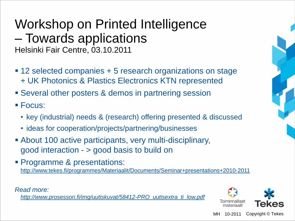
Workshop on Printed Intelligence – Towards applicationsHelsinki Fair Centre, 03.10.2011
12 selected companies + 5 research organizations on stage
+ UK Photonics & Plastics Electronics KTN represented
Several other posters & demos in partnering session
Focus:
• key (industrial) needs & (research) offering presented & discussed
• ideas for cooperation/projects/partnering/businesses
About 100 active participants, very multi-disciplinary,
good interaction - > good basis to build on
Programme & presentations:http://www.tekes.fi/programmes/Materiaalit/Documents/Seminar+presentations+2010-2011
Read more:http://www.prosessori.fi/img/uutiskuvat/58412-PRO_uutisextra_ti_low.pdf
10-2011MH

Copyright © Tekes
Theme of the workshop
Not clearly defined area, … think openly, widely – even wildly!
Still a new field – a lot of opportunities to build something new & useful!
Highly multi-disciplinary approach needed
Combination of
−materials technology
−a set of different processing techniques
−understanding of applications
(needs/new opportunities)
10-2011MH
Material and processing solutions
leading to cost-effective
mass-manufacturable intelligent structures
Printed Intelligence
Printed Electronics
Printed Functionality
???
Copyright © Tekes
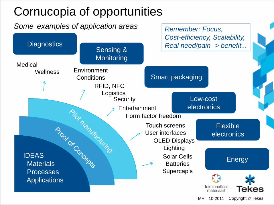
Cornucopia of opportunitiesSome examples of application areas
10-2011MH
IDEAS
Materials
Processes
Applications
Smart packaging
Energy
Diagnostics
Flexible
electronics
Touch screens
User interfaces
Solar Cells
Batteries
Supercap’s
Form factor freedom
Sensing &
Monitoring
Low-cost
electronics
Logistics
Entertainment
Environment
Conditions
RFID, NFC
Medical
Wellness
Security
OLED Displays
Lighting
Remember: Focus,
Cost-efficiency, Scalability,
Real need/pain -> benefit...

Copyright © Tekes
About markets now and in future...according to IdTecEx, 2011 (www.IDTechEx.com)
Market for Printed & potentially Printed Electronics in 2011:
$2.2 Billion - BUT most are not printed and are on glass today
• OLED Displays $1 Billion (Vacuum processed on glass, mainly cellphones)
• Photovoltaics $360 million (only CIGS, OPV, DSSC Most are CIGS – on glass)
• Other inks: $420 million (RFID tag antennas,membrane circuits, bus bars etc.)
• Sensors: $130 million (Glucose test strips, ECG sensors, touch screens)
• E-paper displays $180 million (E-readers)
• Inorganic AC Electroluminescent displays $80 million
(Signage, Promotional items, Consumer electronics)
• Others $30 million (Printed Batteries, Logic, Memory, Electrochromic displays…)
Forecast 2011-2021
• Increasing growth after 2015
• Expected market size about $45 Billion in 2021
esp. OLED & electrophoretic displays, photovoltaics…
10-2011MH
2011 2021
” ”
Copyright © Tekes
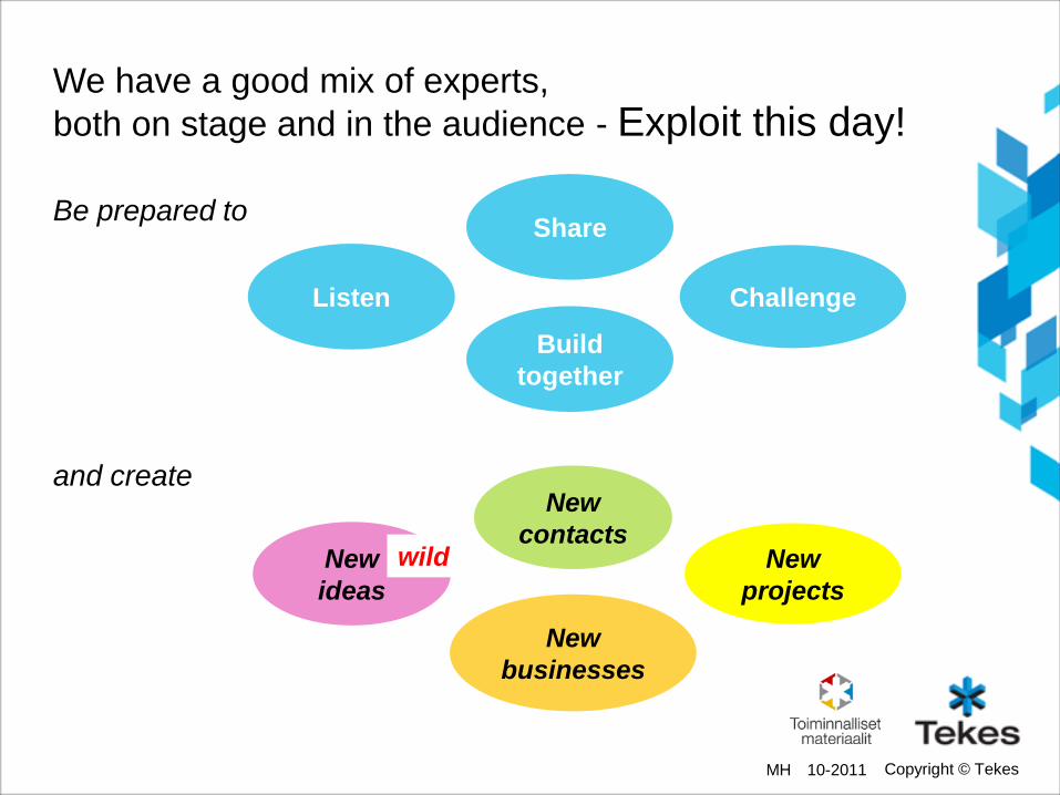
We have a good mix of experts,
both on stage and in the audience - Exploit this day!
Be prepared to
and create
10-2011MH
Listen
Share
Build
together
Challenge
New
ideas
New
businesses
wild New
projects
New
contacts
Copyright © Tekes
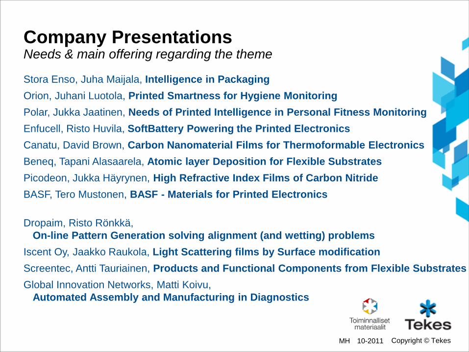
Company PresentationsNeeds & main offering regarding the theme
Stora Enso, Juha Maijala, Intelligence in Packaging
Orion, Juhani Luotola, Printed Smartness for Hygiene Monitoring
Polar, Jukka Jaatinen, Needs of Printed Intelligence in Personal Fitness Monitoring
Enfucell, Risto Huvila, SoftBattery Powering the Printed Electronics
Canatu, David Brown, Carbon Nanomaterial Films for Thermoformable Electronics
Beneq, Tapani Alasaarela, Atomic layer Deposition for Flexible Substrates
Picodeon, Jukka Häyrynen, High Refractive Index Films of Carbon Nitride
BASF, Tero Mustonen, BASF - Materials for Printed Electronics
Dropaim, Risto Rönkkä,
On-line Pattern Generation solving alignment (and wetting) problems
Iscent Oy, Jaakko Raukola, Light Scattering films by Surface modification
Screentec, Antti Tauriainen, Products and Functional Components from Flexible Substrates
Global Innovation Networks, Matti Koivu,
Automated Assembly and Manufacturing in Diagnostics
10-2011MH

Copyright © Tekes
Research offering
VTT, Prof. Harri Kopola, Printed Intelligence from Research to
Industrialization
Åbo Akademi, Prof. Jouko Peltonen, From Component Development to
Device Demonstrators in Printed Functionality
Tampere University of Technology, Prof. Donald Lupo, Devices, Circuits
and System Integration in Printable and Organic Electronics
Aalto University, Prof. Esko Kauppinen, High Quality Thin Film Field
Effect Transistors (TFT-FET) from Carbon Nanotubes
University of Oulu, Dr. Tapio Fabritius, Movement Sensors by Printing
Technologies
+ several posters and demos
10-2011MH

Copyright © Tekes
Some conclusions Good technology basis exist in Finland
• Competence and expertize in VTT and universities
• Several companies with own technology & know-how
• New companies formed recently
BUT more boost and muscles needed
Application needs should drive / show direction
• ”Pain/problem” to be solved -> real benefits or totally new markets
• More active partners needed (from Finland and abroad)
• Companies (product owners) in particular
Now it is time to go towards business
• Proof-of-concept type work -> early piloting
• Involve marketing people, designers, etc.
- to build business cases not only technology demos
Open mind & positive attitude: opportunities to build new businesses or
expand current ones (not necessarily replace them)
10-2011MH

Copyright © Tekes
Specific funding possibilities
Functional Materials Programme funding 2011
• Funding Call for research organizations is open now – until 31.10.2011
• Main themes: 1. Printed Functionality
2. Commercialising research findings
• NOTE! Company projects – funding can be applied continuosly!
• Build company projects parallel to research driven projects
− Support each other; applications needs identified; faster transfer of results
See details: http://www.tekes.fi/fi/community/Hakuajat/472/Hakuaika/1320?name=Toiminnalliset+materiaalit+ohjelman+rahoitushaku+tutki
musorganisaatioille
Remember also EU funding possibilities
• Research Groups: e.g. FP 7 calls, COLAE network
• For SMEs: e.g. Eurostars, Research for SMEs
10-2011MH

Copyright © Tekes 10-2011MH
Sun et al,Nature Nanotechnology (2011) 6, 156–161
World's first carbon nanotube based
integrated circuits on plastic substrate
Example of a PROPOSED PROJECT (Prof. Esko Kauppinen, Aalto)develop roll-to-roll manufacturing &novel applications – collaboration with VTT/Oulu & Nagoya University (Mizutani-Ohno group)
Already developed jointly
by Aalto and Nagoya Univ.
Future technology to be developed
1atm,
continuous, fast
formation
Room temp. process
Onto any substrate
High
performance
flexible ICs
Copyright © Tekes
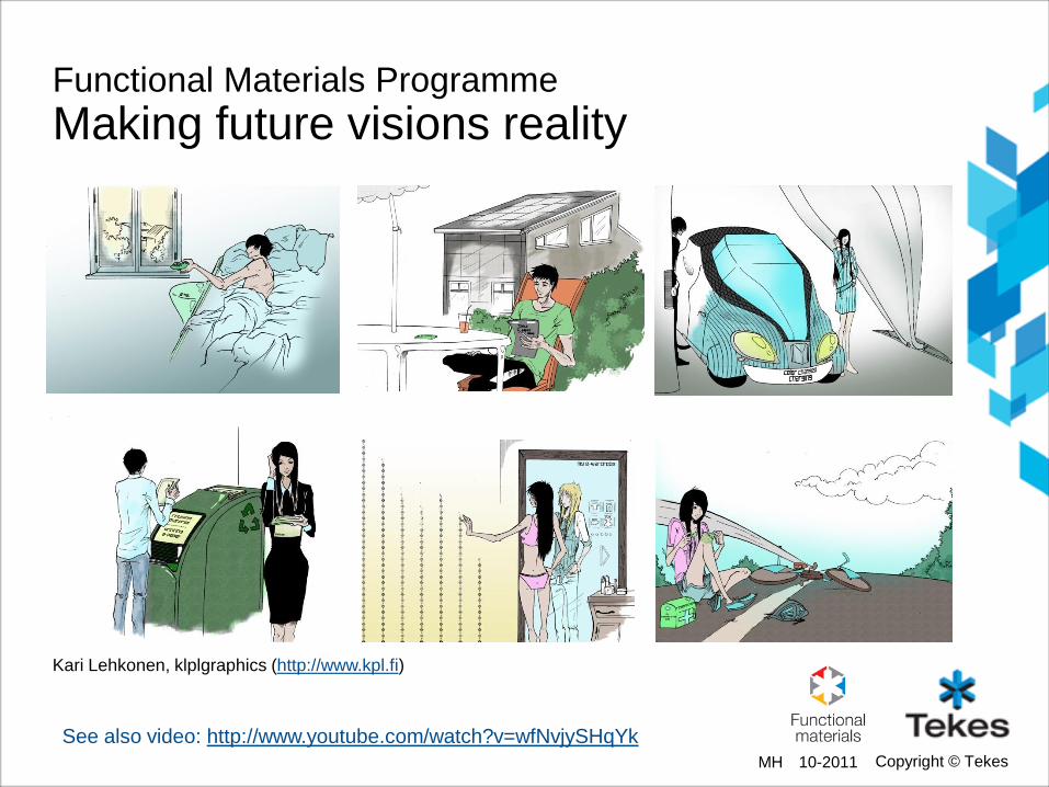
Functional Materials Programme
Making future visions reality
Kari Lehkonen, klplgraphics (http://www.kpl.fi)
See also video: http://www.youtube.com/watch?v=wfNvjySHqYk
10-2011MH

Copyright © Tekes
Join us to create the future together!
Programme manager: Markku Lämsä, [email protected]
Programme coordination: Markku Heino, Spinverse [email protected]
Further information: www.tekes.fi/eng/materials
10-2011MH