functional timing analysis of vlsi circuits containing
TRANSCRIPT

UNIVERSIDADE FEDERAL DO RIO GRANDE DO SUL
INSTITUTO DE INFORMÁTICA
PROGRAMA DE PÓS-GRADUAÇÃO EM COMPUTAÇÃO
Functional Timing Analysis
of VLSI Circuits Containing Complex Gates
by
JOSÉ LUÍS ALMADA GÜNTZEL
Thesis submitted as partial fulfillment of the requirementsfor obtaining the degree of “Doutor em Ciência da Computação”
Prof. Ricardo Augusto da Luz ReisAdvisor
Porto Alegre, November 2000.

2
C.I.P. - Catalogação na Publicação
Güntzel, José Luís AlmadaFunctional Timing Analysis of VLSI Circuits Containing Complex Gates / by
José Luís Almada Güntzel. – Porto Alegre : PPGC da UFRGS, 2000.182 p. : il.
Tese (doutorado) – Universidade Federal do Rio Grande do Sul. Programade Pós-Graduação em Computação, Porto Alegre, BR – RS, 2000. Orientador:Reis, Ricardo Augusto da Luz.
1. Microeletrônica. 2. Ferramentas de CAD para Microeletrônica. 3.Verificação de Timing. 4. Análise de Timing. 5. Portas Lógicas Complexas.I. Reis, Ricardo Augusto da Luz. II. Título.
UNIVERSIDADE FEDERAL DO RIO GRANDE DO SULReitora: Profª. Wrana PanizziPró-Reitor de Ensino: Prof. José Carlos Ferraz HennemannPró-Reitor Adjunto de Pós-Graduação: Prof. Philippe Olivier Alexandre NavauxDiretor do Instituto de Informática: Prof. Philippe Olivier Alexandre NavauxCoordenadora do PPGC: Profª. Carla Maria Dal Sasso FreitasBibliotecária Chefe do Instituto de Informática: Beatriz Regina Bastos Haro

3
Acknowledgments
This work is the result of more than five years of research. During this time manypeople contributed to its development and I will probably forget to mention somebody thathelped me along the way.
First of all, I thank my family for their support and constant encouragement, mainlyduring the difficult periods when I could not see the light at the end of the tunnel. I also thankmy fiancée, Margarida, for her friendship and patience, accepting my excuses for eachworking weekend.
I also thank my advisor, Ricardo Reis, for his unconditional support and friendship.
Timing analysis became the focus of my research since the time I have spent at theLaboratoire d´Informatique, de Robotique et de Micro-électronique de Montpellier - LIRMM(France). I acknowledge Prof. Daniel Auvergne who kindly accepted me in his working group.I thank Nadine Azemard, my direct supervisor, and Séverine Cremoux, my team mate, fortheir willingness in working with me and for their patience with my poor French skills.During 1996, the year I spent in France, I had the chance of meeting many interesting peoplewhose friendship I really miss. Ricardo Pires, Véronique Moreda, Daniel Séverac, ÉricVanier, Jean-Michel Daga, Lionel Torres and many others, I thank you for all moments wehave shared together. Still during that time, I have the support and friendship of many otherpeople that I previously knew. I am particularly indebted with André Reis, who has hosted meduring the first two weeks in France. I also thank André Reis for our discussions on logicsynthesis, technology mapping, timing analysis, BDDs, test and so many other philosophicaltopics! I should also mention Renato Ribas, Gilson Wirth and Reginaldo Tavares for bothtechnical and philosophical discussions.
During the other four years of research, I had the help of undergraduate and graduatestudents. I specially thank Ana Cristina Medina Pinto for helping me in the tediously task oftesting so many versions of path enumeration algorithms. I also thank her for our endlessdiscussions on ATPG-based timing analysis. I also thank Guilherme Dal Pizzol for helpingme with the ad hoc timing analysis of carry skip adders and Eduardo d´Ávila for the firstimplementation of the extended three-valued timed calculus for complex gates.
During all the five years I could always count with the support and friendship ofFernando Moraes, including some “on-line” helps during my stay in France, for what Isincerely acknowledge.
Although timing analysis is my main topic of interest, I could not resist checking othertopics. In this sense, I thank to Fernanda Lima, Luigi Carro and Marcelo Johann for havingshared several discussions and some papers on Masterslices Architectures for FPGAs. I alsothank to Fábio Klein Ferreira for developing the path-based power evaluation tool, as finalpaper of his undergraduate course.
I could not forget to mention the friendship and support of all colleagues of the UFRGSMicroelectronics Group (GME) along all these years. So, thank to all of you: Marcelo Johann,Marcus Kindel, João Leonardo Fragoso, Fernanda Lima, Érika Cota, César Zeferino, EduardoCosta, Jung Choi, Leandro Indrusiak, José Luis Gómez, Rosaldo Rossetti, Alessandro Adario,Márcio Kreutz and so many others. I also thank to all professors of the GME for their

4
unquestionable contribution to my research profile: Ricardo Reis, Sergio Bampi, TiarajuWagner, Altamiro Susin, Luigi Carro, Marcelo Lubaszewski and Flávio Wagner.
During the first four years of this work, including the year I was in France, I had thefinancial support of CAPES Brazilian Agency (Coordenação de Aperfeiçoamente de Pessoalde Nível Superior), for what I gratefully acknowledge.
Finally, I thank God for providing me with so many opportunities of learning!

5
To Margarida

6

7
Table of Contents
List of Abbreviations ……………...………………..………………………..……… 9
List of Figures ……………………………………….…………………..……….…… 11
List of Tables ……………….……………………….….……...……………..……… 13
Abstract ………………….……………………...………………....……………………. 15
Resumo ………………….………………….……………………....…………………… 17
1 Introduction ……………….………..………………………………......…………… 19
1.1 Thesis Organization ……….………...………………………………....…………… 22
2 The Timing Analysis Approach …………………………………………..…….. 25
2.1 Topological Timing Analysis ……….…..……………………….………………….. 26
2.2 False Paths ……..……………………………………..…………………………….... 28
2.3 Functional Timing Analysis and Circuit Delay Computation Models …..……... 30
2.4 Component Delay Models ……..………….……………………………..………….. 32
2.5 Gate Delay Computation Models ...………...………..………………..……………. 34
2.6 Robustness and Correctness of FTA Algorithms ……………………...…………... 35
2.7 Delay Computation Models, Path Sensitization and FTA Algorithms …………. 36
3 Timing Analysis Related Terminology ……………………………………….. 39
3.1 Boolean Algebra ……………………………………………………………………... 39
3.2 Test Generation Terminology …..…………………………………………….…..... 42
3.3 Delay Testing and Timing Analysis Terminology ……………………………….. 46
4 Path Sensitization Criteria and Delay Computation Models …………... 49
4.1 Delay Computation Models and the Robustness Property ……………………...... 49
4.2 Path Sensitization Criteria ………………………………………………………… 54
4.2.1 Static Sensitization ……………………….….…..……………………………...…... 54
4.2.2 Static Cosensitization ……………………….…...……………………………...…... 57
4.2.3 Viability Analysis …..…………………………………...………………………...… 59
4.2.4 Exact Floating-Mode Sensitization …………………………..…………………… 61
4.2.5 Other Sensitization Criteria …………………...………………..…………………… 64
4.3 Qualitative Comparison Between Sensitization Criteria ………………….……. 64
5 Functional Timing Analysis Algorithms …………………………………….. 67
5.1 Classification of FTA Algorithms and Historical Review ………………………... 67
5.2 ATG-Based Single Path Sensitization Algorithms ………………………………. 70

8
5.2.1 The Best-First Search Path Enumeration Procedure of Yen et al. [YEN89] ……… 71
5.2.2 Best-First Search Path Enumeration Considering Different Fall and Rise GateDelays …………...…………………………..…………………………………….…
74
5.3 ATG-Based Multiple Path Sensitization Algorithms …………...……………..…. 76
5.3.1 The PODEM Algorithm …………...………………………………..………………. 76
5.3.2 Cube Simulation ………….….…………………..………..………………….…… 78
5.3.3 Timed Test Generation …………...……………………………..…………………... 81
5.3.4 Backtrace …………...………………………………..……………………………. 82
5.4 SAT-Based Multiple Path Sensitization Algorithms ……………………………. 84
5.4.1 Philosophy of the SAT-Based Method of [MCG93] ………….…………….….…. 84
5.4.2 Ternary Delay Simulation and Waveform Calculus …………………..…………... 85
5.4.3 Computing the Floating Delay under the XBD0 Model ………………….………… 90
6 Functional Timing Analysis of Combinational Circuits ContainingComplex Gates ……………………………..……………………………………….
95
6.1 Technology Mapping and Layout Generation for Circuits Containing ComplexGates 6.1 ……..……..……..……………………..................…….…………………... 95
6.1.1 Simple Gates, General Complex Gates and Static CMOS Complex Gates …...….. 98
6.2 The Applicability of Existing Functional Timing Analysis Techniques forCircuits Containing Complex Gates ……..………................................................….…..
100
6.3 ATPG-Based FTA of Circuits Containing Complex Gates 6.3 …………..…….…. 101
6.3.1 Extending the Timed-Calculus to Complex Gates …............................................….. 106
6.3.2 The Floating Delay of a Gate …...…............................................................................ 109
6.3.3 Gate Delay Computational Models and Timed Forward Implication for SCCGs …... 113
6.3.4 Timed Backward Implication for SCCGs …..........................................................….. 116
7 Conclusions .................................................................................................................. 119
7.1 Future Work .................................................................................................................. 121
Appendix 1 The Need for Functional Timing Analysis: a Case Study ….... 123
Appendix 2 Gate Delay Computation Models and the Complexity of Best-First Search Procedures .......................................................................
129
Appendix 3 Análise de Timing Funcional de Circuitos VLSI ContendoPortas Complexas ..................................................................................
137
References ……..……………….……...…………………………..……………….….. 173

9
List of Abbreviations
ATPG Automatic Test Pattern Generation
BDD Binary Decision Diagram
CAD Computer-Aided Design
BFS Breadth-First Search
CMOS Complementary Metal-Oxide Silicon
Csa Carry-skip Adder
DAG Direct Acyclic Graph
DFS Depth-First Search
EDA Electronic Design Automation
FTA Functional Timing Analysis
FSM Finite State Machine
FUCAS FUll Custom Automatic Synthesis
iff if and only if
mdt Maximal Delay to Node t
MSF Multiple Stuck Fault
ps picoseconds
SCCG Static CMOS Complex Gate
sgd single gate delay
spgd single pair gate delay
SAT satisfiability
SSF Single Stuck Fault
TTA Topological Timing Analysis
VLSI Very Large Scale Integration
XDB Extended Bounded Delay Model
XBD0 Extended Bounded-Zero Delay Model

10

11
List of Figures
FIGURE 1.1 - Synchronous sequential circuit model. ………………………….…….. 20
FIGURE 2.1 - Combinational circuit example. ………………………………….……. 26
FIGURE 2.2 - Processed DAG for the circuit example of figure 2.1. ………………….. 27
FIGURE 2.3 - First example of false path: Hrapcenko’s circuit. …………..………….. 28
FIGURE 2.4 - Second example of false path: a 2-bit carry-skip adder. ……………..….. 29
FIGURE 2.5 - The delay of circuits depends upon the type of inputs considered. ……. 31
FIGURE 3.1 - Cube representation for the 3-dimensional Boolean space. .…………….. 40
FIGURE 4.1 - Transition delay with fixed gate delays: test circuit (a) and timingdiagrams (b),(c). …………………………………………………………. 50
FIGURE 4.2 - Transition delay with fixed gate delays: another instance of the testcircuit of figure 4.1a (a) and timing diagrams (b),(c). …………………. 51
FIGURE 4.3 - Transition delay with unbounded gate delays: test circuit of figure 4.1awith unbounded delays (a) and timing diagrams (b),(c). …………...…. 52
FIGURE 4.4 - Conditions for Static Sensitization. ……………………………...…….... 55
FIGURE 4.5 - Example of static sensitization of a path. ………………………………. 55
FIGURE 4.6 - Static sensitization on the csa example. ……………………………….… 56
FIGURE 4.7 - Static sensitization underestimating circuit delay. ………...…………….. 57
FIGURE 4.8 – Conditions for static cosensitization. …………………………………… 58
FIGURE 4.9 - Example of static cosensitization of paths. …………………………...… 58
FIGURE 4.10 - Static cosensitization can be pessimistic. ………………………….…... 59
FIGURE 4.11 - Conditions for viability. ………………………….…………………..... 60
FIGURE 4.12 - Example of viable path that is not statically cosensitizable. …………... 60
FIGURE 4.13 - Conditions for exact floating-mode sensitization. …………………....... 62
FIGURE 4.14 - First example of exact floating-mode sensitization. ……………….… 62
FIGURE 4.15 - Second example of exact floating-mode sensitization. ………………… 62
FIGURE 4.16 - Third example of exact floating-mode sensitization. ……………….….. 63
FIGURE 4.17 - Fundamental assumptions made in single-vector exact floating mode. 64
FIGURE 4.18 - Comparison between sensitization criteria. ………………………….... 65
FIGURE 5.1 - Single path sensitization procedure. ………………………………....….. 71
FIGURE 5.2 - DAG for circuit of figure 2.1, pre-processed according to the best-firstsearch procedure. ………………………………………………………... 72
FIGURE 5.3 - k-list structure initialized with the first partial paths of the circuit offigure 5.2. ……………………………………………….……………….. 74

12
FIGURE 5.4 - k-list structure for the best-first procedure that considers separate fall andrise delays. …………………………………………………………... 75
FIGURE 5.5 - Pseudocode for the topmost call of the PODEM algorithm. ……………. 77
FIGURE 5.6 - Pseudocode for the first search procedure. ……………………………… 77
FIGURE 5.7 - Pseudocode for the second search procedure. …………………………… 78
FIGURE 5.8 - PODEM algorithm example. ………………………………………….…. 79
FIGURE 5.9 - Binary decision tree for PODEM algorithm. ……………………………. 80
FIGURE 5.10 - Cube simulation using timed calculus. ………………………………. 81
FIGURE 5.11 - Timed test generation example. ……………………………………… 83
FIGURE 5.12 - Backtrace example. ………………………………………...………… 84
FIGURE 5.13 - Basic operation of SAT-based FTA algorithms. ………………………. 85
FIGURE 5.14 - Example of ternary waveform. …………………………………………. 87
FIGURE 5.15 - Delay model for a gate in the wave space. ……………………………... 88
FIGURE 6.1 - Physical design flow using the FUCAS layout generation strategy ……... 97
FIGURE 6.2 - Example of SCCG …….….........................................................………… 99
FIGURE 6.3 - Elements of the virtual library SCG(2,2) …….…......................………… 99
FIGURE 6.4 - Timed-test generation procedure applied to a single-output circuit …….. 102
FIGURE 6.5 - Pseudo-code for the topmost call of the timed-test generation procedure . 102
FIGURE 6.6 - Pseudo-code for the first search procedure ................................................ 103
FIGURE 6.7 - Pseudo-code for the second search procedure ............................................ 104
FIGURE 6.8 - Pseudo-code for the imply procedure ......................................................... 105
FIGURE 6.9 - Three-valued timed calculus for group 1 ................................................... 107
FIGURE 6.10 - Three-valued timed calculus for group 2 ................................................. 107
FIGURE 6.11 - Three-valued timed calculus for group 3 ................................................. 107
FIGURE 6.12 - Example of SCCG: logic-level symbol (a), transistor schematics (b) andfunction tree (c) ................................................................................................ 108
FIGURE 6.13 - Using the three-valued timed calculus for evaluating a SCCG ................ 109
FIGURE 6.14 - The relationship between floating mode (a) and transition mode (b) ...... 110
FIGURE 6.15 - The relationship between floating mode and transition mode: a floatingvector applied to a 3-input NAND gate (a) and the 8 underlying pairs ofvectors (b) ........................................................................................................ 111
FIGURE 6.16 - Success (a) and fail (b) conditions for the timed-test generationprocedure ......................................................................................................... 113
FIGURE 6.17 - Delay of a SCCG under a floating cube ................................................... 115
FIGURE 6.18 - Backward implication in a SCCG by using forward implication rules .... 117

13
List of Tables
TABLE 3.1 – Main properties of the Boolean algebra. ……..…………………………... 39
TABLE 3.2 - Truth-table for the 5-valued AND operation. ……..……………………... 45
TABLE 3.3 - Truth-table for the 5-valued OR operation. ………….…………………... 45
TABLE 5.1 - Classification of existing FTA algorithms. ……………………………….. 69
TABLE 5.2 - Timed calculus with unknown values. ………………………….…….… 80
TABLE 5.3 - Truth table for the AND function in ternary algebra. …………………..… 86
TABLE 5.4 - Truth table for the OR function in ternary algebra. ……………………..... 86
TABLE 6.1 - Number of elements for various virtual libraries [DET87] ......................... 99
TABLE 6.2 - Three-valued timed calculus for a 2-input AND gate .................................. 105
TABLE 6.3 - Three-valued timed calculus for a 2-input OR gate ..................................... 105
TABLE 6.4 - Generalized three-valued timed calculus for n-input simple gates .............. 106
TABLE 6.5 - Three-valued timed calculus for evaluating SCCGs ................................... 108
TABLE 6.6 - Relationship between floating model vectors and transition model vectors 112
TABLE 6.7 - Equivalence between floating and transition modes for the SCCG offigure 6.17 ......................................................................................................... 115

14

15
Abstract
The recent advances in CMOS technology have allowed for the fabrication of transistorswith submicronic dimensions, making possible the integration of tens of millions devices in asingle chip that can be used to build very complex electronic systems. Such increase incomplexity of designs has originated a need for more efficient verification tools that couldincorporate more appropriate physical and computational models.
Timing verification targets at determining whether the timing constraints imposed to thedesign may be satisfied or not. It can be performed by using circuit simulation or by timinganalysis. Although simulation tends to furnish the most accurate estimates, it presents thedrawback of being stimuli dependent. Hence, in order to ensure that the critical situation istaken into account, one must exercise all possible input patterns. Obviously, this is notpossible to accomplish due to the high complexity of current designs. To circumvent thisproblem, designers must rely on timing analysis. Timing analysis is an input-independentverification approach that models each combinational block of a circuit as a direct acyclicgraph, which is used to estimate the critical delay.
First timing analysis tools used only the circuit topology information to estimate circuitdelay, thus being referred to as topological timing analyzers. However, such method mayresult in too pessimistic delay estimates, since the longest paths in the graph may not be ableto propagate a transition, that is, may be false. Functional timing analysis, in turn, considersnot only circuit topology, but also the temporal and functional relations between circuitelements.
Functional timing analysis tools may differ by three aspects: the set of sensitizationconditions necessary to declare a path as sensitizable (i.e., the so-called path sensitizationcriterion), the number of paths simultaneously handled and the method used to determinewhether sensitization conditions are satisfiable or not. Currently, the two most efficientapproaches test the sensitizability of entire sets of paths at a time: one is based on automatictest pattern generation (ATPG) techniques and the other translates the timing analysis probleminto a satisfiability (SAT) problem.
Although timing analysis has been exhaustively studied in the last fifteen years, somespecific topics have not received the required attention yet. One such topic is the applicabilityof functional timing analysis to circuits containing complex gates. This is the basic concern ofthis thesis. In addition, and as a necessary step to settle the scenario, a detailed and systematicstudy on functional timing analysis is also presented.
Keywords: design verification of VLSI circuits, timing analysis, functional timing analysis(FTA), path sensitization problem, critical delay estimation, complex gates,automatic test pattern generation (ATPG), satisfiability (SAT).

16
17
TITLE: “ANÁLISE DE TIMING FUNCIONAL DE CIRCUITOS VLSI CONTENDOPORTAS COMPLEXAS.”
Resumo
Os recentes avanços experimentados pela tecnologia CMOS tem permitido a fabricaçãode transistores em dimensões submicrônicas, possibilitando a integração de dezenas demilhões de dispositivos numa única pastilha de silício, os quais podem ser usados naimplementação de sistemas eletrônicos muito complexos. Este grande aumento nacomplexidade dos projetos fez surgir uma demanda por ferramentas de verificação eficientes esobretudo que incorporassem modelos físicos e computacionais mais adequados.
A verificação de timing objetiva determinar se as restrições temporais impostas aoprojeto podem ou não ser satisfeitas quando de sua fabricação. Ela pode ser levada a cabo pormeio de simulação ou por análise de timing. Apesar da simulação oferecer estimativas maisprecisas, ela apresenta a desvantagem de ser dependente de estímulos. Assim, para seassegurar que a situação crítica é considerada, é necessário simularem-se todas aspossibilidades de padrões de entrada. Obviamente, isto não é factível para os projetos atuais,dada a alta complexidade que os mesmos apresentam. Para contornar este problema, osprojetistas devem lançar mão da análise de timing. A análise de timing é uma abordagemindependente de vetor de entrada que modela cada bloco combinacional do circuito como umgrafo acíclico direto, o qual é utilizado para estimar o atraso do circuito.
As primeiras ferramentas de análise de timing utilizavam apenas a topologia do circuitopara estimar o atraso, sendo assim referenciadas como analisadores de timing topológicos.Entretanto, tal aproximação pode resultar em estimativas demasiadamente pessimistas, umavez que os caminhos mais longos do grafo podem não ser capazes de propagar transições, i.e.,podem ser falsos. A análise de timing funcional, por sua vez, considera não apenas a topologiado circuito, mas também as relações temporais e funcionais entre seus elementos.
As ferramentas de análise de timing funcional podem diferir por três aspectos: oconjunto de condições necessárias para se declarar um caminho como sensibilizável (i.e., ochamado critério de sensibilização), o número de caminhos simultaneamente tratados e ométodo usado para determinar se as condições de sensibilização são solúveis ou não.Atualmente, as duas classes de soluções mais eficientes testam simultaneamente asensibilização de conjuntos inteiros de caminhos: uma baseia-se em técnicas de geraçãoautomática de padrões de teste (ATPG) enquanto que a outra transforma o problema deanálise de timing em um problema de solvabilidade (SAT).
Apesar da análise de timing ter sido exaustivamente estudada nos últimos quinze anos,alguns tópicos específicos não têm recebido a devida atenção. Um tal tópico é a aplicabilidadedos algoritmos de análise de timing funcional para circuitos contendo portas complexas. Esteconstitui o objeto básico desta tese de doutorado. Além deste objetivo, e como condição sinequa non para o desenvolvimento do trabalho, é apresentado um estudo sistemático e detalhadosobre análise de timing funcional.
Palavras-chave: verificação de projeto de circuitos VLSI, análise de timing, análise de timingfuncional (FTA), sensibilização de caminhos, estimativa do atraso crítico,portas complexas, geração automática de padrões de teste (ATPG),solvabilidade (SAT).

18

19
1 Introduction
The remarkable advances achieved by CMOS fabrication technology in the last threedecades have made possible the amazing expansion that consumer electronics market hasbeen going through. Thanks to the continuously increasing transistor integration densityoffered by CMOS technology, ever more complex systems can be integrated on a single chip,allowing more sophisticated electronic equipment to be available at relatively low prices.
Obviously, higher transistor densities are obtained by reducing the dimensions of on-chip components. To a first approximation, reducing transistor and wiring dimensions wouldlead us to believe that higher clock frequencies could easily be achieved, since smallertransistors switch faster. Indeed, this used to be a well-established law for a long time.However, since CMOS technology has allowed for submicronic devices, some up till thenignored side effects have grown in importance, resulting in new phenomena that partiallyinvalidate the previously mentioned law. One of such phenomena, probably the most cited inrecent years, is the dominance of wiring delays over gate delays, as a consequence of theincrease in RC factor of interconnections.
Since the 80’s the increasing complexity of electronic systems has made mandatory theuse of automatic synthesis tools. Electronic design automation (EDA) tools covering all stepsof circuit design, from the behavioral to the physical level, were developed. Such toolsincorporated efficient algorithms, able to treat systems with hundreds of thousand gates.However, by the time submicronic technologies began to be used, the models used by thesetools for estimating performance were revealed completely wrong. Since then, a lot of efforthas been concentrated on developing more accurate circuit models, able to account for theside effects resulting from submicronic technologies.
Among the available EDA tools, those devoted to design verification are currentlyplaying a key role. Since it is not practical to directly prototype the circuit in order to test it onits working environment, designers must rely on verification tools to certify, beforefabrication, that the circuit will operate properly. Besides certifying proper operation, one mayalso desire to explore the target technology in all its extension, looking for achieving themaximal performance. Hence, we can conclude that verification tools must offer a minimumof reliability.
Timing verification targets at determining whether the timing constraints imposed tothe design may be satisfied or not. More strictly, timing verification is concerned withestimating the critical delay of circuits and the maximal operating frequency, in case ofclocked circuits.
As any other type of verification, the accuracy of timing verification is completelydependent on the accuracy of the adopted circuit models. By circuit models it is meant notonly the physical delay model used to quantify the delay of each component, but also themodels for computing circuit component delay and the circuit delay itself. Such models arestrongly dependent on the circuit operation model, that is, whether the circuit is assumed tooperate in a synchronous or in an asynchronous manner.
Many of the existing timing verification techniques target at synchronous sequentialcircuits. Thus, let us consider the issues arriving while estimating the maximal operatingfrequency of a sequential circuit that may be represented as a Mealy finite state machine(FSM). The Mealy FSM model, depicted by figure 1.1, divides the combinational part into

20
two distinct blocks: the next state logic and the output logic [GAJ99]. The next state logiccomputes the next state variables while the output logic is responsible for the output signals. Ifmemory elements are edge-triggered flip-flops, then at each active clock edge the next state isloaded into the flip-flops, becoming the current state. At that time, the next state begins to becomputed by the next state logic. Outputs may change as a consequence of a change in currentstate (stored in the flip-flops) or as a consequence of a change at the inputs or even both.
D1 Q1
Q1
FF1
D2 Q2
Q2
FF2
D3 Q3
Q3
FF3
...next state
logicoutput logic
I1 I2 Ik
O1
O2
On
...
...
outputs
inputs
clock
D1 Q1
Q1
FF1
D2 Q2
Q2
FF2
D3 Q3
Q3
FF3
...
D1 Q1
Q1
FF1
D1 Q1
Q1
FF1
D2 Q2
Q2
FF2
D2 Q2
Q2
FF2
D3 Q3
Q3
FF3
D3 Q3
Q3
FF3
...next state
logicnext state
logicoutput logicoutput logic
I1I1 I2I2 IkIk
O1O1
O2O2
OnOn
...
...
outputs
inputs
clock
FIGURE 1.1 - Synchronous sequential circuit model.
Consider that the next state logic has maximum and minimum propagation delays Tnext
and tnext, respectively, while the output logic has maximum and minimum propagation delaysTout and tout, respectively. Consider also that the edge-triggered flip-flops present maximumpropagation delay Tff, setup time ts and hold time th. Then, in order to assure correct circuitoperation, the following conditions must be observed:
• τ > max (Tff + Tnext + ts) , (Tff + Tout) , where τ is the clock period
• tnext > th
• circuit’s inputs must be stable and valid for a period greater than Tnext + ts beforeeach active clock edge.
The derived conditions above are quite conservative but allow for a safe synchronousoperation. The first condition assures that clock period is long enough to accommodate theworst case delay within the next state loop (Tff + Tnext + ts) and the worst case delay for theoutput logic (Tff + Tout ). The second condition avoids excessively short clock periods thatcould prevent flip-flops from sampling valid new states. The third condition assures that theinput signals to the next state logic are computed in time, such that all outputs of this blockare stable and valid for an amount of time equal or greater than ts before the next clock edge.
In fact, the third condition may be disregarded if extra flip-flops are used to synchronizethe inputs. Moreover, the first condition is conservative enough to allow the outputs to besampled using the same clock phase applied to state flip-flops. In case a different phase isavailable, this condition could be loosen to τ > max (Tff + Tnext + ts) , Tout .

21
Let us go a little bit further on evaluating how circuit operation model may affect theprocedure for estimating the clock frequency. Consider that the already discussed circuitoperation model is to be adopted and assume that inputs are synchronized by flip-flops thatare controlled by the same clock applied to the state flip-flops. If the variation in propagationdelays of flip-flops is not significant, one may assume that each combinational block operatesin a completely synchronous manner, in that propagation delay is a consequence of twoconsecutive input vectors. However, if the propagation delays of flip-flops vary significantly,combinational blocks operate in an asynchronous manner, as fast sequences of input vectorswere applied to the circuit before its outputs settle to their final values.
Another important issue is the critical delay estimation of combinational blocks, whichis a complex task per se. The most conservative approach relies on using the topologicaldelay, that is, the delay of the longest path in the circuit. However, more accurate techniquestest whether the longest path or paths are able to propagate transitions1.
The considerations stated in the last two paragraphs are very important for developingtiming verification tools that are stimuli-independent or use simplified component models,such as switch level simulators. However, in case of detailed circuit simulation, the circuitoperation model is implicitly considered in the context of circuit-level detailed models, suchas differential equations or signal waveforms.
Electrical simulation is the most accurate method for verifying the timing requirementsof CMOS circuits. Detailed electric level simulators such as Spice [NAG75] represent thecircuit as a network of passive and active elements (resistors, capacitors, inductors andcontrolled sources) and solve the related system of ordinary linear differential equations foreach time step of the simulation run. Unfortunately, electric level simulation demands hugeexecution times even for moderately small circuits. To speedup electrical simulationrelaxation methods have been proposed and used (equation relaxation in ELOGIC [KIM86]and waveform relaxation in RELAX [LEL82], for instance). Even though, electricalsimulation cannot be used solely for determining time performance of state-of-the-art digitaldesigns.
An alternative to electrical simulation is timing simulation. Timing simulation isaccomplished by simplified electric level simulators, such as XPSIM [BAU88], or enhancedswitch level simulators, such as Motis [CHA75], TV [JOU87] and Crystal [OUS85]. Timingsimulation is faster than electrical simulation because it uses less accurate models. In case ofCrystal and TV, for instance, effective resistances are used to model transistors. On the otherhand, results are less accurate than those obtained through electrical simulation.
There are three serious difficulties in using the simulation approach (electrical or timingsimulation) for verifying the timing requirements of circuits. The first is the execution time toaccomplish all necessary computations, which was already discussed. A second problem is theeffort required for preparing a set of input patterns, since the simulation approach is stimulidriven. Third one, and maybe the most stringent, is ensuring that the set of patterns exercisesthe critical situation that determines the circuit’s critical delay. This constitutes a problem dueto the high complexity of current digital designs. For instance, a combinational network withn inputs exhibits 2n possible input vectors. Even for medium combinational blocks, where n isof the order 100, exhaustive circuit simulation would not be possible. Hence, determining aminimum set of vectors that guarantees to find the circuit delay is not trivial.
1 This is known as the critical path problem, which is discussed along the next chapters of this thesis.

22
Due to these difficulties, the input-independent approach has replaced simulation forestimating the critical delay of VLSI circuits. This approach, known as timing analysis2,represents each combinational block of the circuit as a weighted direct acyclic graph (DAG),where nodes represent gates and edges represent connections. The weights of nodes and edgesrepresent the delays of gates and connections, respectively. The critical delay of eachcombinational block is determined by analyzing the length of the paths in the graph.
The most naïve solution relies on disregarding logic behavior of gates and assuming thedelay of the longest path as the critical delay of the combinational block. Hence, the criticaldelay problem of a combinational block is reduced to finding its longest path, which can besolved in linear time by the well-known topological sort algorithm [COR90]. Such approach,referred to as static or topological timing analysis (TTA), was probably born with the IBMPERT Project [KIR66] and was used by other timing analyzers such as [HIT82].
However, there may not exist any input pattern that exercises the longest path in thecircuit, or equivalently, it may never transmit any signal transition. In this case, the criticaldelay may be smaller than the delay of the topologically longest path. Paths that nevertransmit a signal transition are called false paths [HRA78] (or unsensitizable paths). Acircuit may contain many false paths. In order to improve the accuracy of delay estimates,timing analysis tools must take path sensitizability into account. Unfortunately, performingfalse path-aware timing analysis constitutes a NP-complete problem and thus, manyassumptions must be done in order to obtain safe critical delay estimates.
Although some work has been done for allowing automatic generation of false path-freecircuits (e.g., [KEU91][SAL94][KUK97a][PRA00]), most of available high-level synthesissystems may generate circuits with false paths [BER91].
In late years a lot of research has focused on developing efficient timing analysisalgorithms that consider the path sensitization problem. But as long as CMOS technologyevolves very fast and higher clock rates are continuously being demanded, improving theaccuracy of critical delay estimation is still an issue of relevant importance in designverification.
Furthermore, some specific topics have not received sufficient attention yet. One suchtopic is the applicability of functional timing analysis (FTA), i.e., false path-aware timinganalysis, to circuits containing complex gates. Some works on logic synthesis have reportedthe possibility of area reduction and performance improvements when static CMOS complexgates (SCCGs) are used [REI98][RIE96]. However, timing analysis of circuits containingcomplex gates is rarely mentioned in the literature. Indeed, only some of the existingalgorithms can handle such circuits. The study of functional timing analysis applied to circuitscontaining complex gates is the main concern of this thesis.
1.1 Thesis Organization
This thesis is organized as follows. Chapter 2 reviews the basic issues of the timinganalysis approach. Topological timing analysis is discussed in detail and the reason why itmay furnish too pessimistic estimates is addressed. Functional timing analysis is thenintroduced. The component delay models and the circuit delay computation modelsunderlying FTA tools are presented. The basic properties to assure that FTA furnishes safecritical delay estimates are also presented.
2 In this thesis, the term timing verification is used to refer to any method that can verify timing requirements ofcircuits. However, the term timing analysis will only be used for input-independent timing verification methods.

23
Chapter 3 presents a comprehensive collection of definitions that are necessary tounderstand the theory behind FTA and the related algorithms.
Chapter 4 is devoted to the path sensitization problem. The three most importantsensitization criteria, the static sensitization, viability and the exact floating sensitization arepresented.
The main issues that are considered in the development of a FTA tool are presented andclassified in chapter 5. This includes the adopted sensitization conditions and the method usedto determine whether the sensitization conditions are satisfiable. This chapter also discussessome of the most important existing algorithms.
Chapter 6 justifies the use of CMOS complex gates in the design of VLSI circuits. Italso discusses the limitations of existing timing analysis methods for estimating the delay ofcircuits containing such type of gates. A new solution for performing functional timinganalysis of circuits containing complex gates is then proposed. This solution relies onextending the three-valued timed calculus used within the timed-test generation procedure ofDevadas et al. [DEV93a] in order to handle complex gates in a friendly manner (i.e., withoutusing macro-expansion). The advantages and disadvantages of the proposed solution arediscussed.
Finally, some concluding remarks are offered.
The appendices bring extra information on specific topics. Appendix 1 justifies theimportance of taking into account false paths by studying false paths in carry-skip adders.Appendix 2 presents an informal evaluation of the time complexity of the best-first algorithm,used by path enumeration-based FTA tools. Appendix 3 is an extended abstract of the thesisin portuguese.
This thesis may also be used as a quick introduction to the basic concepts on timinganalysis and timing models used within high level and logic level synthesis algorithms.Chapters 1 and 2 introduce most of the necessary concepts without using any formalism. Forthose interested in going further, the definitions presented in chapter 3 are essential, though.

24

25
2 The Timing Analysis Approach
During the 80’s, as design complexity augmented quickly, the verification of timingrequirements of circuits through simulation became impractical due to the increasingexecution time demanded and also to the difficulty in determining a safe set of input vectorsthat proven to exercise the critical delay situation. Then, the attention was turned to stimuli-independent verification methods, in opposition to simulation methods.
But even before, more precisely in 1966, Kirkpatrick and Clark [KIR66] proposed theuse of the management method called PERT (Program Evaluation Review Technique) toestimate the critical delay of circuits. In their work, a combinational block was represented asa weighted direct acyclic graph (DAG), with the nodes representing circuit gates and the edgesrepresenting circuit connections. The longest path in the DAG was discovered by using thetopological sort algorithm [COR90] and its delay was assumed to be the critical delay of theblock.
The idea of using PERT to estimate critical delay of combinational circuits was retakenby Hitchcock in the development of its “Timing Analyzer” program [HIT82], which alsocame up with the innovative concept of signal time slacks. Also the expression timinganalysis, currently used by EDA community to designate any input-independent timingverification tool, seems to be borrowed from Hitchcock’s work.
However, there may not exist any input pattern3 that exercises the longest path in thecircuit, in the sense that no signal transition (or event) can propagate along it. Since PERT-based timing analysis disregards the logic behavior at circuit’s nodes, it may furnish aneedless pessimistic critical delay estimate. In addition, the fact that PERT-based timinganalysis considers only circuit topology has motivated some authors to call it topologicaltiming analysis (TTA) (e.g., [DEV94]).
Paths that never transmit any signal transition are called false paths [HRA78]. (Someauthors also use the term unsensitizable paths.) A circuit may contain many false paths. Theproblem of determining whether a path may be exercised or not is referred to as the pathsensitization problem or as the (general) false path problem [DU89]. According to[MCG89], although false paths were known for some time, the first complete discussion onthis topic was due to Hrapcenko, who designed a parametric circuit to show that for somecircuits the true delay could differ from the topological critical delay [HRA78].
Early timing analysis tools took into account false paths by allowing case analysis. TheTiming Analysis program (TA) from Hitchcock [HIT82], for instance, had a facility calleddelay modifiers that could be used to indicate paths that, in the designer’s opinion, wouldnever be activated. However, as long as manual detection of all false paths in complex circuitsis impossible, since early it became clear that automatic false path detection should bepursued. The first attempts for including automatic false path detection was the work of Brandand Iyngar [BRA88] and that of Benkoski et al. [BEN87]. Since then, most of research intiming analysis has concentrated on this issue, looking for algorithms that could lead toaccurate delay estimates in a reasonable amount of time. More recently, timing analysis
3 The majority of existing timing analysis techniques do not consider explicitly all possible input patterns.Actually, the definition of which patterns are allowed depends on how inputs are assumed to be made of, what istaken into account by the adopted circuit delay computation model (see section 2.3).

26
techniques that consider false paths have been termed functional timing analysis (FTA)[ASH95][KUK97]. Such terminology is also adopted in this text.
This chapter is concerned with the basic aspects underlying the timing analysisapproach, with special attention to the models used in FTA. Section 2.1 describes how thetopological sort algorithm is adapted to perform TTA. In section 2.2 the false path problem isintroduced by means of two circuit examples. Section 2.3 discusses delay computation modelsin the context of FTA, showing that circuit delay computation depends on the type of inputsconsidered. It also associates the possible types of inputs to circuit operation models and tothe so-called modes of operation. Section 2.4 summarizes the most relevant physicalcomponent delay models, while section 2.5 presents the gate delay computation modelscommonly used in FTA tools. Section 2.6 discusses the correctness and robustness propertiesof timing analysis algorithms. Such properties allow us to evaluate whether a given FTAtechnique is able to furnish safe delay estimates or not and in affirmative case, how accuratesuch estimates are. Finally, section 2.7 gives an overview on the spectrum of modelpossibilities while implementing a FTA tool.
2.1 Topological Timing Analysis
Any timing analysis technique represents each combinational block as a weighted DAG.In this DAG nodes are associated with gates and edges are associated with connections(sometimes, nets). The delay of each gate (connection) may be stored at the respective node(edge). Another possibility is to concentrate (or lump) at each node (or edge) the sum of thedelays of the gate and its output connections. This choice depends on the data structure usedto store DAG information and on the accuracy of physical models used to estimate component(gates and connections) delays. Dummy nodes, i.e., nodes with zero delay, represent primaryinputs and primary outputs. Frequently, source and terminal (dummy) nodes are added to theDAG to transform it into a canonical DAG. This may help the development of graph traversalfunctions that operate both forward and backwards. In a canonical DAG representation, anycomplete path assumes the form (s, es, v0, e0, v1, e1, …, vn, en, vn+1, et, t), where v0 and vn+1
represent the primary input and the primary output, respectively, s and t are the source andterminal nodes and es and et are dummy edges. Figure 2.2 shows a DAG representation for thecircuit of figure 2.1.
a
NAND4
NOR0
b
c
NAND5
NAND6
NAND7
INV1
INV0
NAND2
NAND3
NAND1
NAND0
z
d
FIGURE 2.1 - Combinational circuit example.

27
Topological timing analysis finds the longest path in the DAG, which corresponds to thepath with greatest delay, and assumes it as responsible for the critical delay of the circuit. Thisis accomplished by using the topological sort algorithm [COR90], which is known to executein linear time with respect to the graph size. It also may compute the time slack of signals,which can be used in a performance optimization step.
2
NAND3a
b
c
d
s
2
NAND5
2
NAND6
2
NAND4
3
NOR0
1
INV1
2
2
NAND7
2
0
0
0
0
0
2
z tNAND1
0
1
INV0
NAND0
NAND2
0,2,2
Notation
At,Rt,S
At= arrival time of s ignal
Rt = required time of signal
S = slack of signal
td
0,2,2
0,2,2
1,2,1
0
2,4,2
2,4,2
3,4,1
4,5,1
6,7,1
4,8,4
6,7,1
8,9,1
8,10,2
9,10,1
11,12,1
td = delay of the gate
FIGURE 2.2 - Processed DAG for the circuit example of figure 2.1.
Let us illustrate the topological timing analysis procedure on the circuit of figure 2.1.(DAG of figure 2.2 holds the timing information gathered from such procedure.) For thecurrent example, assume that graph edges represent circuit nets (instead of connections).Assume also that the delay of the gates and their output nets are lumped at graph nodes. Forany circuit signal e a 3-tuple of timing values is calculated and annotated at the related graphedge: the arrival time of e, At(e) which is the time that the signal at edge e settles to its final(steady state) value, the required time of e, Rt(e), which is the time at which the signal at e isrequired to be stable and the slack S(e), calculated as the difference between the required timeand the arrival time (Rt(e)-At(e)). The arrival times of the primary inputs and the requiredtimes of the primary outputs are set by the timing constraints for the block under analysis.Non-zero arrival times for the primary inputs may be necessary in case of hierarchicalanalysis. The topological analysis begins by computing the arrival times for each signal in aforward manner, beginning from the primary inputs. The arrival time of a signal e, which isthe output of node v, is calculated by:
)d()At(max)At( iivee += (2.1)
where d(v) is the delay of the gate represented by v and ei is the set of input signals to v. Oncethe arrival times of all primary outputs are calculated (or alternatively, node t is reached), theprocedure performs a backward step for calculating the required times of signals, using therequired times of primary outputs. The required time of a signal e is calculated by:
[ ] ))d()Rt(min)Rt( jjjvee −= (2.2)
where vj represents the gates that have e as fanin and ej are the output edges (nets) of suchgates. Having calculated the required time of a signal, its slack can also be computed.

28
Sometimes this computation of arrival times, required times and slacks is called delay tracethrough the network [DEV94].
Once the graph has been completely processed, the topologically longest path ortopological critical path is the path where each signal has the minimum slack and can beeasily traced. In this example the topological critical path is (s, d, NAND7, NOR0, NAND2, INV0,NAND1, z, t), with delay 11 and slack 1. The slack is also a measure of the criticality of pathsand may be used for identifying gates for resizing and/or buffer insertion points in case of adelay optimization procedure [JU91][JOU87][CHE93a].
Although topological timing analysis may overestimate the critical delay of circuits, itsurely is an upper bound on the critical delay of a combinational circuit. Indeed, most ofexisting high-level and architectural-level synthesis tools still use it as a fast means ofverifying the timing requirements of designs, since at these levels there is an implicit lack ofaccuracy in physical delay models of components. However, as operating frequency of VLSIdesigns enters the gigahertz range, more accurate delay estimates are demanded. Hence,considering path sensitizability is mandatory. In the next section the false path problem isintroduced by means of two circuit examples.
2.2 False Paths
Currently, timing, power, area and testability are the criteria used to guide designoptimization during synthesis. Unfortunately, most of optimization procedures introduceredundancies into designs [KEU91], which constitute one known source of false paths.
If input vector v does not activate a path P, then P is said not to be sensitizable by v. If Pis not sensitizable by any input vector, then P is said to be false.
Consider Hrapcenko’s circuit [HRA78] shown in figure 2.3. Assume that all gates havedelay equal 1 and wires have zero delay. Its topologically longest paths are P1=(i1, G1, G2, G3,G4, G6, G7, G8, h) and P2=(i2, G1, G2, G3, G4, G6, G7, G8, h), both with delay 7. However,while i3=0, no signal transition can propagate from a to b. Similarly, while i3=1, no signaltransition can propagate from d to f. As long as a signal cannot assume two logic values at thesame time, the only possibility to sensitize P1 and P2 is allowing a sequence of vectors to beapplied at circuit’s inputs such that i3=1 at time 1 and i3=0 at time 4. However, if only pairs ofvectors are allowed, then the previous case is not possible. Then, paths P1 and P2 are false andthe circuit delay is less than 7.
i1
G1 G2
G5
G8
G3 G4 G6 G7
i2
i3
ab
cd
e
fg
h
i4i5
i6
i7
FIGURE 2.3 - First example of false path: Hrapcenko’s circuit.

29
Some classes of circuits are designed to purposely make the topologically longest pathsfalse, as a strategy for reducing its critical delay. One such a class is composed of carry-skipadders [KEU91][DEV94][LAM94]. Figure 2.4 shows a 2-bit carry skip adder (csa2). Higherorder adders may be obtained by connecting together csa2s through the carry chain. In thiscase the topologically longest path will include the carry chain, which in a single csa2 as theone showed by figure 2.4 corresponds to path P=(c0, n0, n1, n2, n3, n4, c2), in bold. Thus, todetermine the critical delay of a higher order csa adder, one must begin by analyzing thesensitizability of such path.
Suppose all gates of the csa2 of figure 2.4 have unit delay and wires have zero delay.Assuming only pairs of vectors at the circuit’s inputs, in order to sensitize path P, p0, g0, p1,g1, ctrl_n and n5 must be 1 at times 0, 1, 2, 3, 4 and 5, respectively. However, if p0, g0, p1and g1 are made fixed at 1, ctrl_n will be fixed at 0 and no transition will reach n4. On theother hand, no input pair of vectors satisfies p0=1 at time 0, p1=1 at time 2 and ctrl_n=1 attime 4. Thus, path P is false.
Moreover, late transitions at c0 (i.e., transitions arriving after time t=0) do not changethe sensitizability of path P. This means that in any higher order adder made up from this csa2the topologically longest path is false. Appendix 1 presents a detailed ad hoc analysis of csas,using fixed non-unit delay and assuming different fall and rise gate delays.
a0
c0
b1
a1
b0
p0
p1
g0
g1
s0
c2
s1
n0
ctrl_n
n1n2 n3
mux2-1
n4
n5
FIGURE 2.4 - Second example of false path: a 2-bit carry-skip adder.

30
2.3 Functional Timing Analysis and Circuit Delay Computation Models
As mentioned in chapter 1, the accuracy of any timing verification tool is completelydependent on the accuracy of the adopted circuit models. Furthermore, in the specific case oftiming analysis tools, some assumptions on circuit operation are also required to improvecritical delay estimation, what will become clear in the following paragraphs.
The topological timing analysis procedure presented in section 2.1 may lead tosignificant overestimation of critical delay because it ignores the logical behavior of circuitgates. Considering different fall and rise gate delays in that procedure is easily accomplishedand may result in significant improvement of the estimation accuracy [GÜN98][GÜN98a]. Ina certain manner, the use of different fall and rise gate delays may be seen as a very crudemodel for circuit operation, which, however, does not take false paths into account.
Due to the false path phenomenon, the critical delay of a circuit may be less than thedelay of its topologically longest path. The difference between the topological delay and theactual critical delay cannot be neglected in the context of an automated design process sincethe designer does not have total control on the resulting generated structure. Further, even forsome hand-made designs the delay estimated by a topological analysis may be too pessimisticand more accurate estimations would be highly desirable. (That is the case of carry-skipadders [KEU91][LAM94][DEV94] and some multipliers.)
In order to take false paths into account, it is necessary to revise the concept of criticaldelay of a (combinational) circuit. A path-based definition would state that “the critical delayof a circuit is the delay (or length) of its longest sensitizable path”, also mentioning that “theremay exist more than one critical path” [CHE93]. Although correct, this definition is quitelimited since not all of the false path-aware timing analysis algorithms work on a per-pathbasis.
A more general definition can be found by examining the circuit operation model andrealizing that the essence of timing analysis should be the capture of the exact instant at whichthe slowest circuit output(s) settle to its (their) steady-state value(s). Of course, one possiblesolution relies on testing the sensitizability of each circuit path, beginning by the longest one.However, this is not the only possible solution. Indeed, state-of-art timing analysis techniques(or algorithms) operate on sets of paths at a time, what generally results in less computationtime. Timing analysis algorithms that considers false paths fall into the functional timinganalysis (FTA) category, and will be discussed in chapter 5.
Having posed the FTA problem from a new point of view, it is possible to redefine thedelay of a circuit. The delay of a circuit under a given input pattern is the minimum amountof time after which all of its outputs are settled to their steady-state values. By extension, thecircuit’s critical delay corresponds to its greatest delay, considering all possible inputpatterns. For the sake of simplicity, we may refer to the critical delay of a circuit just as delayof the circuit (or circuit delay), since this is the parameter of interest in this thesis.
Note that the previously stated definitions implicitly consider path sensitizability.However, what exactly constitutes an input pattern is not clear. This point was intentionallyleft open in order to make the definition of critical delay independent of the circuit operationmodel. In reality, the definition of what constitutes a valid input pattern depends on how thecircuit is assumed to operate and will be considered within the circuit delay computationmodel.
The concept of circuit delay computation model was motivated by the observation thatthe delay of a circuit depends on the nature of its inputs, that is, whether the inputs are

31
assumed to be made of pairs of vectors or sequences of vectors. To illustrate this, considerthe test circuit of figure 2.5a (borrowed from [LAM94]), with gate delays as assigned insideeach gate. The longest path of this circuit is (a, c, f, y), with delay 5. If the inputs areconsidered to be made of pairs of vectors, then the latest output transition occurs at t=1. Apossible input combination that generates a latest output transition is shown in figure 2.5b. Onthe other hand, if the inputs are considered to be made of sequences of vectors, then the latestoutput transition occurs at t=3. A possible input vector sequence that leads to this late outputtransition is shown in figure 2.5c. These results confirm that circuit delay may differaccording to the type of applied inputs.
a
b
c
d
e
f y
3
2
1
1 1
(a)
a
b
c
d
e
f
y
t0
v0v1 v2
delay=3
a
b
c
d
e
f
y
t0
v0 v1
delay=1
(b) (c)
FIGURE 2.5 - The delay of circuits depends upon the type of inputs considered.
In order to compute the delay by a pair of vectors, it is assumed that a vector v1 isapplied at t=−∞ and a second vector v2 is applied at t=0. The delay of a circuit is then definedas the maximum arrival time of the last output transition over all possible pairs of vectors.From the definition it becomes clear that all circuit nodes are assumed to be settle to theirstable values with respect to v1 by the time vector v2 arrives.
Using the delay by pairs of vectors to estimate the circuit’s critical delay is equivalent toassuming that the circuit operates in a fully synchronous manner. This type of operation hasbeen referred to as the transition mode and the critical delay thus obtained is calledtransition delay of the circuit [DEV92].

32
It has been conjectured that the transition delay is the exact delay of a circuit [SIL99].Indeed, this would be true if one could always guarantee a fully synchronous operation ofcombinational blocks within synchronous circuits. However, memory elements may presentdifferent propagation times that can lead to the misalignment of inputs. Also, a supposedbenefit of the transition delay method is that, besides the delay estimation, it generates the pairof vectors responsible for this delay, thus allowing the certification of this delay throughcircuit simulation.
An implementation of transition delay calculation is proposed in [DEV92] and[DEV94a]. It uses symbolic simulation along with some sophisticated delay computationmodel. Further improvements concerning event suppression were proposed in an attempt toreduce the time complexity of this symbolic simulation based implementation [DEV94b]. Thetransition delay method presents severe disadvantages that have prevented its use in practicalFTA tools, however. Firstly, the search space for determining the critical input vector pairsituation is 22n, with n being the number of primary inputs to the circuit. Secondly, the delaycomputation model used, the bounded model (see section 2.4), makes the symbolic simulationextremely expensive from the computation's point of view.
The problems with delay by pairs of vectors (transition mode) have motivated themassive use of the single vector approach. The single vector approach is an approximation ofthe delay by sequences of vectors. It conservatively assumes the nodes of a circuit to bearbitrary, i.e. "floating", before they are settle by a single input vector v. The delay of thecircuit is the latest settling time over all possible single vectors vi. The assumption of floatingnodes comes from the fact that the circuit may be still propagating the input vectors appliedbefore v, what would cause the circuit nodes to be floating. In the literature, the assumption ofthe single vector approach is incarnated by the designation of “floating mode of operation”[CHE91] and the delay thus obtained is referred to as the floating delay of the circuit.
The only known implementation of delay by sequence of vectors is presented in[LAM93] and [LAM94]. It is based on a sophisticated formalism called timed Booleanfunctions (TBFs), which is claimed to unify the Boolean and the timing behavior of circuits.The problem with this implementation is that due to the complex formulation, it demandssignificant computation effort, mainly if mode detailed delay models are to be used.
Although delay by sequences of vectors would be desirable, the majority of existingFTA algorithms adopts the single-vector (floating) delay computation model due to its ease ofimplementation and smaller computational cost. Moreover, it has been reported in [LAM94]that for most practical circuits made of simple gates the delay by sequences of vectors and thesingle vector delay are coincident. And for the cases where they are not coincident, singlevector delay is an upper bound on the actual circuit delay, while the delay by sequences ofvectors is the exact delay. Also, single-vector techniques may use many of already existingtest generation algorithms.
2.4 Component Delay Models
Component delay models refers to the physical model (also called circuit-level model)used to estimate the delay of each circuit component, thus obtaining individual delayinformation that will be used to determine the delay of the circuit as a whole. This informationis generally expressed in terms of equations that use parameters derived from extensivetransistor-level and/or device-level simulation of circuit components.

33
Logic synthesis tools as SIS [SEN92] generally use the linear delay model, which is thesimplest physical model. In the linear delay model of SIS, for instance, the delay across a pini, d(i), of a gate is given by:
d(i) = A(i) + B(i) × CL(i) (2.3)
where A(i) is called transport delay for the gate at pin i, B(i) is the inverse of the drivecapability of the gate and CL(i) is the total capacitive load of the net represented by i, lumpedat the output of the gate. Although this simple model does not take into account someimportant features of CMOS technology (e.g., short channel devices, slow input ramps andbody effect), it is still used by the majority of logic synthesis tools because it does not requiretoo expensive computations.
However, the study of more sophisticated delay models appears as a major subject of thework done in the timing verification field during the first half of the 80’s. Probably, this is dueto the fact that these works were directly related to the development of new microprocessors.This was the case of Ousterhout’s Crystal [OUS85] and Jouppi’s TV [JOU87], which wereused in the timing validation of the RISC II and MIPS microprocessors, respectively.
Crystal divides the circuit into stages to evaluate the delay. A stage is defined as a chainof transistors and nodes between a signal source and a place where the signal is used. Hence,a stage may represent not only the MOS transistor chain up to the gate output but also anypass transistor chain being driven by the gate. A natural consequence of this switch-levelmodeling of MOS circuits is that the delay of connections would be implicitly consideredwithin stages. Crystal has three physical delay models: the lumped RC model, the lumpedslope model and the distributed slope model. In the lumped RC model each transistor type ischaracterized by two resistance values, being one for the case when the transistor istransmitting a logic 0 and another when it is transmitting a logic 1. These values are given inOhms per square and are multiplied by the transistor’s W/L to obtain the effective resistance.The delay through a stage is computed by lumping all resistances and capacitances. Thelumped slope model incorporates information about waveform. Each waveform is representedby its inversion time and its rise time. This tries to model the effect of the load being drivenby the stage on the effective resistance, leading to a more accurate delay estimation. Thelumped model is too pessimistic in estimating the delay of distributed capacitances. Thedistributed slope model is similar to the slope model except that, instead of assuming all RClumped, it uses the results of Penfield and Rubinstein [RUB83] for the delay of RC trees.
TV uses also the Penfield-Rubinstein model but with two simplifications: only thewaveform estimate is computed, instead of the bounds, and only one path is assumed openthrough a tree of pass transistors. This reduces the accuracy of the model because theinfluence of the input ramp slope is only roughly considered.
The formerly cited physical models use linear elements to approximate the behavior oftransistors which is non-linear in its essence. Thus, it is not a surprise that a significant errormay occur. Looking for more accurate delay estimations, Horowitz has proposed the use ofnon-linear elements for dealing with both transistors and interconnection networks [HOR84].In his formulation the input ramp slope is modeled by a hyperbolic function while thetransistor is modeled by a simple quadratic function.
A third possibility for delay modeling is to use explicit formulation. According to thisapproach the delay is estimated by using a closed formulation that includes parameters fortechnology characterization. Some of these parameters may be obtained from deviceextraction while others may come from exhaustive electrical simulation. But once the targettechnology is appropriately characterized, the delay of circuit components is estimated only by

34
using the formulae, without any other supporting means as, for instance, electrical simulation.Examples of explicit analytical formulations are the alpha-power model [SAK88] and theexplicit formulation of [DES88].
In the explicit formulation of [DES88] the delay of an inverter with minimum W and Lis used as a standard measure for a given technology. To this delay quantity various correctionterms may be applied in order to generalize the delay estimation to nor and nand gates,possibly with Wn/Wp≠1. To consider the effect of slow input ramp a correction term wasadded latter to the formulation [AUV90]. Recently, the formulation was revised in order toaccount for the effects of submicronic technologies [DAG99].
Recent advances in CMOS technology have shrinked device dimensions to nanometers.Many electrical effects that were formerly disregarded in micronic technologies became veryimportant in current submicronic (or nanometric) technologies and constitute sources of errorsthat may compromise the correct operation of complex designs. A practical example of suchphenomenon is the effect of circuit interconnections. In submicronic technologies the delay ofinterconnections is considerable and frequently dominates the delay of circuit gatesthemselves. Hence, physical delay models for interconnections begin to play a very importantrole in the delay estimation. The basic models for interconnection analysis are those thatevaluates RC networks as the Elmore’s [ELM48], Sakurai’s [SAK83], Penfield-Rubinstein[RUB83], Horowitz [HOR84] and also the models of Crystal. With the advent of submicronictechnologies interconnection analysis has come into focus again and several works thatsimultaneously consider gate and connection delays have been published. A referential workwas the interconnection analysis program called RICE [RAT94], that uses a technique knownas AWE (Asymptotic Waveform Evaluation), which is based on the moments of the impulseresponse. Currently, several other works are being developed for modeling the delay of gatesand connections for submicronic technologies (e.g., [FOR97][HIR98]).
A more detailed discussion on physical models for component delay calculation isbeyond the scope of this work. A good review on this issue may be found in [UEB95], whichalso presents an analytical semi-empirical delay model that uses a latency time and aneffective linear resistance to model the exponential region of the output curve of a stage.
2.5 Gate Delay Computation Models
The simplest gate delay computation model is known as the fixed delay model[DEV94]. It assumes that the delay of a gate is a fixed value d. A natural extension to thismodel is to assign a fixed delay value di to each input i of a gate. Another variation is toconsider separate falling and rising delays by either assigning a single pair of delays [df,dr] tothe gate or assigning a pair of delays [dfi,dri] to each input i. The assignment of a fixed delayor a pair of fixed delays per input is also referred to as pin-to-pin delay.
One important issue that arrives in timing analysis is that it is not intended to providethe critical delay of a single manufactured instance but the delay of the entire family ofmanufactured circuits of the same design. In this sense, the use of TTA along with maximalindividual gate delays leads just to an upper bound on circuit delay. However, currentsubmicronic designs demand more accurate delay estimations (at least tighter upper bounds),what, from the computational's point of view, can be accomplished by using the FTAapproach. On the other hand, the use of maximal gate delays in FTA is not sufficient to assurethat the estimated circuit delay really represents an upper bound over the entire family of

35
manufactured circuit instances: due to the sensitization phenomenon, maximal individual gatedelays may result in an underestimation of circuit delay, what would be an unacceptableerroneous prediction. This phenomenon is known as the monotone speedup failure[MCG91] and will be commented in more detail in the next section.
In order to assure that FTA will not underestimate circuit delay, gate delays must bespecified within a bounded interval [dmin,dmax], where dmin and dmax represent the minimumand the maximum delay of the gate, respectively. This is the so-called bounded delay modeland is the model underlying the transition delay computation. The bounded delay may also beassigned in pin-to-pin format. A modification on the bounded delay model consists ofconsidering dmin =0, which is commonly referred to as unbounded delay model (meaningunbounded bellow)4. As it will be shown in the next section, this is the model used forcomputing the floating delay under the monotone speed up property.
The previously described gate delay models implicitly divide signal magnitude into twovalues, either 0 or 1. Obviously, a more detailed analysis could be performed if signals wererepresented with a multi-valued logic. In the case of a ternary logic, for instance, a signal mayassume one among the values (0,1,X) at a time, where X represents signal magnitudesbetween the 0-threshold and the 1-threshold. Ternary logic has been used for hazard detectionand logic simulation [SEG89]. In [MCG93], ternary logic was formalized to be used in theFTA context, with the addition of the third state (X) to both bounded and unbounded models,originating the extended bounded delay model (XBD) and the extended bounded-zerodelay model (XBD0), respectively.
2.6 Robustness and Correctness of FTA algorithms
In order to furnish a safe delay estimate any FTA algorithm must satisfy two properties:robustness and correctness. By safe estimate it is meant a delay value that reflects a tightupper bound on the delay of all design instances after fabrication. (In fact, the later statementis an informal definition of the correctness property.)
The robustness property was originally named monotone speedup property by McGeerand Brayton [MCG89][MCG91]. It basically says that the use of maximal individual gatedelays does not guarantee the estimated delay to be an upper bound on the actual delay of thewhole family of manufactured circuit instances. As a consequence, the use of such anestimated delay value would be useless for design validation, since it may exist one or morecircuit instances exhibiting greater delays.
Let us examine the circumstance under which the robustness property would fail. In theanalysis of a single design instance, the assumption of maximal individual gate delays maylead to a sensitization situation in which the longest path declared as sensitizable exhibits adelay which is smaller than that of the topologically longest path. It means that there is at leastone unsensitizable path with delay greater than the circuit’s topological delay. Suppose that asecond instance of the same design is to be analyzed. Suppose also that one or more gates inthis other instance present individual delays which are smaller than their correspondentmaxima. Due to Boolean and timing relations between circuit gates, the path sensitizabilityanalysis may lead to a situation in which the path declared as sensitizable exhibits a delaywhich is greater than the delay of the longest sensitizable path of the former analyzed
4 Maybe, a more appropriate designation would be bounded-zero delay model.

36
instance. This failure in circuit delay estimation was originally called the monotone speedupfailure [MCG89].
Let C1,C2,…,Cn be n fabricated instances of a combinational circuit C. The robustnessproperty can be defined as follows. (Taken from [SIL99], with modifications.)
Definition 2.1: robustness property
For each true path P in Ci, (i=1, 2 ,…, n) there must exist a true path Q in the slowest Ci
such that d(Q) ≥ d(P), where d(P) (d(Q)) is the length or delay of path P (Q).
By true path it is meant exactly (floating-mode) sensitizable path (see subsection 4.2.4).
Assuring that a FTA algorithm follows the robustness property is not sufficient,however. As observed by several authors (e.g., [MCG89], [CHE93], [PES94]), it is imperativenot to underestimate the critical delay of a circuit. Otherwise, any of the fabricated instancesmay present an erroneous operation.
The correctness property may be defined as follows. (Taken from [SIL99]).
Definition 2.2: correctness property
For each true path P in C, there must exist a path Q such that d(Q) ≥ d(P), where d(P)(d(Q)) is the length or delay of path P (Q), which is sensitizable under the adopted set ofsensitization conditions.
Equivalently, the property says that the set of conditions used to test paths sensitizabilitymust not underestimate the delay of the critical path.
It is clear that while the robustness property refers to the gate delay computation model,the correctness property concerns the circuit delay computation model. The correctnessproperty also appears as “critical path correctness” in [CHE93] and as “delay correctness” in[PES94]. Both [CHE93] and [PES94] also refer to the path sensitization correctness property,according to which a FTA algorithm (and the embedded set of sensitization conditions) isconsidered correct if it may not declare a true path as unsensitizable.
The previously presented properties are used in the evaluation of the existing FTAtechniques, including the set of conditions used to test path sensitization.
2.7 Delay Computation Models, Path Sensitization and FTA Algorithms
Since the middle 80's a lot of work has been developed focusing on algorithms foraccurately determining the delay of circuits (that is, FTA techniques). However, a systematicclassification of existing methods is still very difficult because FTA techniques may differ byvarious aspects:
1. the circuit delay and gate delay computation models,
2. the set of conditions used to test path sensitizability, also called sensitizationcriterion,
3. and the method used to test whether the sensitization conditions are satisfied or not.
Circuit delay and gate delay computation models have already been addressed insections 2.3 and 2.5, respectively

37
Several path sensitization criteria are found in the literature (e.g., [BRA88], [DU89],[MCG89], [PER89], [BEN90], [CHE91], [DEV91] and [DEV93]). The most representativeones, static sensitization [BEN90], static cosensitization [DEV91], viability [MCG89] andexact floating-mode sensitization [CHE91], are presented in chapter 4. Chapter 4 begins byinvestigating the robustness of transition mode and floating mode-based delay estimations.
Sensitization criteria are only a part of FTA algorithms. The other part concerns thedelay computation algorithm (or technique) itself. Delay computation algorithms may work ona per-path basis, testing the sensitizability of one path at a time, or may work on sets ofpaths simultaneously. For testing sensitizability, they may assign logical values to circuitnodes, as done by traditional ATPG methods (ATPG-based), or may use satisfiabilitymethods (SAT-based). Hence, there are various possibilities for computing circuit delay.Such possibilities are further detailed in chapter 5, which also describes some of the mostrelevant methods.
Next chapter reviews the terminology related to FTA.

38

39
3 Timing Analysis Related Terminology
As long as timing analysis uses many concepts from test generation and logic synthesis,a revision of the definitions from these areas is concentrated in this chapter. Other timinganalysis related terminologies, as well as some definitions from delay testing, are alsopresented. The chapter is divided into three sections. The first section presents Booleanalgebra definitions, used in logic synthesis. Test generation definitions are presented in thesecond section. The last section is devoted to the definitions that are common to delay testingand timing analysis areas.
3.1 Boolean Algebra
The binary Boolean algebra, considered in this thesis, is defined by the set B=0,1 andthe operators + and ⋅ , called disjunction and conjunction, respectively, which satisfy thecommutative and distributive laws. The disjunction operator, also called sum or OR operator,has 0 as identity element. The conjunction operator, also called product or AND operator, has1 as identity element.
Any element a ∈ B has a complement, denoted by a , such that a ⋅ a = 0 and a + a = 1.The Boolean algebra differs from an ordinary algebra in that distributivity applies to bothoperations and because of the presence of a complement. Table 3.1 shows the main propertiesof the Boolean algebra.
TABLE 3.1 - Main properties of the Boolean algebra.
a + (b + c) = (a + b) + c associativity
a ⋅(b ⋅c) = (a ⋅ b) ⋅c associativity
a + a = a idempotence
a ⋅ a = a idempotence
a + (a ⋅ b) = a absorption
a ⋅(a + b) = a absorption
(a + b) = a ⋅ b De Morgan
(a ⋅ b) = a + b De Morgan
a = a involution
The multi-dimensional space spanned by n binary-valued Boolean variables is denotedby Bn. It is often referred to as the n-dimensional cube, because it can be graphicallyrepresented as a hypercube. A vertex in Bn is represented by a binary-valued vector ofdimension n. When binary variables are associated with the dimensions of the Boolean space,a vertex can be identified by the values of the corresponding variables.

40
A literal is an instance of a variable or of its complement. For instance, a and a are theliterals associated to the variable a. A product of n literals denotes a vertex in the n-dimensional Boolean space and is considered as a zero-dimensional cube. Products of literalsare frequently called cubes.
Consider the 3-dimensional Boolean space, represented in figure 3.1, with its variablesa, b and c. A vertex in the Boolean space can be expressed by the product of n=3 literals, for
example abc (the symbol ⋅ can be omitted), or equivalently by the row vector [100]. Anarbitrary subspace can be expressed by a product of literals, for example, ab, or by the rowvector [11X], where X means that the third variable can take any value.
111
000 100
110010
101001
011 abc
a’b’c’ ab’c’
abc’a’bc’
ab’ca’b’c’
a’bc
a
c
b
111
000 100
110010
101001
011 111
000 100
110010
101001
011 abc
a’b’c’ ab’c’
abc’a’bc’
ab’ca’b’c’
a’bc abc
a’b’c’ ab’c’
abc’a’bc’
ab’ca’b’c’
a’bc
a
c
b
a
c
b
FIGURE 3.1 - Cube representation for the 3-dimensional Boolean space.
Definition 3.1: completely specified Boolean function
A completely specified Boolean function is a mapping between Boolean spaces. An n-input, m-output Boolean function is a mapping f : Bn α Bm , where Bn=0,1n andBm=0,1m.
An n-input, m-output Boolean function can be seen as an array of m scalar functionsover the same domain, and therefore the vector notation is used.
Definition 3.2: incompletely specified Boolean function
An n-input, m-output incompletely specified Boolean function is a mappingf : Bn α Ym , where Bn=0,1n and Ym=0,1,Xm. The symbol X is used to denote thepoints where the function is not defined and is called don’t care condition.
Definition 3.3: on set, off set and dc set
For each output of an n-input, m-output Boolean function, the subsets of the domain forwhich the function takes the values 1, 0 and X are called on set, off set and dc set,respectively.
Consider a single output Boolean function f.
Definition 3.4: support
Let f(x1,x2,...,xn) be a Boolean function of n variables. The set x1,x2,…,xn is calledsupport of f.

41
Definition 3.5: cofactor
The cofactor of f(x1,x2,..., xi,…,xn) with respect to variable xi is fxi=f(x1,x2,...,1,…,xn). The
cofactor of f(x1,x2,..., xi,…,xn) with respect to variable x i is fxi
=f(x1,x2,...,0,…,xn).
Definition 3.6: Boolean expansion (or Shannon’s expansion)
Let f : Bn α B. Then f (x1, x2 ,..., x i ,..., xn ) = xi ⋅ fx i
+ x i ⋅ fx i
= ( xi + fx i
) ⋅ (x i + f xi)
∇ i=1,2,…n.
Definition 3.7: minterm
Any Boolean function f : Bn α B can be represented as a sum of products of n literals,called minterms of the function, by recursively applying the Shannon’s expansion.
After a complete expansion, a Boolean function can be interpreted as a set of itsminterms.
Frequently, set operators are used instead of Boolean operators. This is becauseoperations and relations on Boolean functions over the same domain can be viewed asoperations and relations on their minterm sets. For example, the sum and the product of twofunctions are the union (Υ) and the intersection (Ι) of their minterm sets, respectively, whileimplication between two functions corresponds to the containment (⊆ ) of their minterm sets.
Definition 3.8: unate/binate function
A function f(x1,x2,..., xi,…,xn) is (positive/negative) unate in variable xi if fxi ⊇ fxi
(fxi ⊆ fxi
). Otherwise it is binate (or mixed) in that variable. A function is
(positive/negative) unate if it is variable (positive/negative) unate in all supportvariables. Otherwise it is binate (or mixed).
Definition 3.9: Boolean difference
The Boolean difference of f(x1,x2,..., xi,…,xn) with respect to variable xi is defined as
∂f / ∂xi = fx i
⊕ fxi
.
The Boolean difference of f with respect to xi indicates whether f is sensitive to changesin input xi. When it is zero, then f does not depend on xi and xi is said to be unobservable.This concept is of great interest in test generation.
Definition 3.10: consensus
The consensus of f(x1,x2,..., xi,…,xn) with respect to variable xi is defined as
Cxi
( f ) = fx i⋅ fx i
.
The consensus of f with respect to xi represents the component that is independent of xi.The consensus can be extended to sets of variables:
Cxi
Cx i+1( f ) = Cxi
( fx i+1⋅ fx i +1
)
Definition 3.11: smoothing
The smoothing of f(x1,x2,..., xi,…,xn) with respect to variable xi is defined as
Sxi
( f ) = fx i+ f xi
.

42
The smoothing of f with respect to xi corresponds to dropping xi from furtherconsideration, as all occurrences of xi were deleted. Obviously, the smoothing may also beextended to sets of variables:
Sxi
Sx i+1( f ) = Sxi
( fx i +1+ f
xi +1) = Sxi+1
( fx i+ f
xi) = Sxi+1
Sx i( f )
Test generation terminology is presented in the sequel.
3.2 Test Generation Terminology
In this thesis a combinational circuit C is represented as a direct acyclic graph (DAG)C=(V,E), referred to as the circuit graph, where V and E are the set of nodes and the set ofedges, respectively. In the circuit graph nodes represent circuit gates while edges representcircuit connections (or circuit nets, whenever explicitly indicated). Graph nodes also representcircuit primary inputs and primary outputs. The primary inputs are nodes with no incomingedges, while all the nodes with no outgoing edges are primary outputs5. PI(C) and PO(C)represent the set of primary inputs and the set of primary outputs of C, respectively. For suchDAG representation the following definitions hold.
Definition 3.12: path, complete path and partial path
A path P in C is an alternating sequence of nodes and edges. In particular, a completeor full path has the form (v0, e0, v1, e1, …, vn, en, vn+1), where edge ei , 1 ≤ i ≤ n,connects the output of node vi to an input of node vi+1. Any node vi , with 1 ≤ i ≤ n, is agate; node v0 is a primary input and node vn+1 is a primary output. A partial path isany path that either does not begin in a primary input or does not end in a primaryoutput. P may also be represented by (v0, v1, …, vn, vn+1) or by (e0, e1, …, en). However,as long as such notations may cause some confusion, they will be used only in thesituations when the complete formalism is not needed.
Let P= (v0, e0, v1, e1, …, vn, en, vn+1) be a path.
Definition 3.13: side-inputs and on-inputs
The inputs of vi other than ei-1 are referred to as side-inputs of vi and are represented byS(vi). The set of all side-inputs along P are referred to as the side-inputs of P, S(P). ei-1 isreferred to as on-path input or P-input or on-input of vi.
Since this thesis is concerned with combinational circuits represented at the logic level,only structural faults are of interest. Structural fault models assume that circuitinterconnections may be affected by shorts and opens. A short is formed by connectionsbetween points that were not intended to be connected together, while opens concerns brokenconnections. In most fabrication technologies, including CMOS, a short between power orground and a circuit line (wire) ei causes the signal to be at a fixed voltage. The correspondinglogical fault consists of signal ei being stuck at a fixed logic value b (b ∈ 0,1), and isdenoted by ei s-a-b. In many technologies, the effect of an open on a unidirectional signal linewith unitary fanout is to make the input that has become unconnected assume a constant logicvalue and hence appears as a stuck fault. Thus, a single logical fault of the type ei s-a-b can
5 These definitions may eventually be changed in case the circuit graph is transformed into a canonical DAG bythe addition of source and terminal nodes. For the rest of this text, either this is irrelevant or will be clearlyindicated.

43
represent many different physical faults: ei open, ei shorted to power or ground, and anyinternal fault in the component driving ei that keeps ei at the logic value b [ABR90].
The test terminology necessary as a background to understand the timing analysis theoryis derived from the stuck model based test generation, which is also the most widely usedmodel.
Definition 3.14: single stuck fault (SSF) model and multiple stuck fault (MSF) model
A circuit is said single stuck faulty if it is assumed to contain a stuck fault in one of itslines (wires). A circuit is said multiple stuck faulty if it is assumed to exhibit two ormore stuck faults.
Although the multiple stuck is a more realistic fault model, most of test generationalgorithms assume the single stuck fault model. In the following terminology the single stuckfault is underlying model.
Definition 3.15: test
A test for a fault ei s-a-b is an input vector that allows for distinguishing a faulty circuitfrom a good circuit.
Generally, most of the points within integrated circuits cannot be accessed. Therefore, itis necessary to provide that by applying the test at the circuit’s primary inputs, at least one ofthe primary outputs of the faulty circuit presents a logic value that is different from thatexpected for a fault-free (i.e., good) circuit.
Definition 3.16: automatic test generation (ATG) or automatic test pattern generation(ATPG)
Automatic test generation or automatic test pattern generation refer to the procedure offinding tests for a given set of faults in a circuit by means of computer programs thatautomatically (and possibly exhaustively) generate tests by using appropriate algorithms.
Let us now consider the problem of generating a test for the fault ei s-a-b in acombinational circuit C. Any ATPG procedure able to generate a test for this fault presentstwo basic steps: fault activation and error propagation. Both steps however may be seen asdirect applications of a generic procedure known as line justification, defined as follows.
Definition 3.17: line justification
Consider a combinational circuit C. Let g be a simple gate (AND, OR, NAND, NOR) inC. g has output e0 and inputs e1, e2, …, ek. Justifying the logic value b at e0 meansfinding an assignment of logic values that applied at the primary inputs of C results in bat e0.
Line justification is a recursive procedure in which a gate’s output is justified by anappropriate assignment of logic values at its inputs and so on, until the primary inputs of thecircuit are reached.
Suppose g is an AND gate. Then there is only one assignment of inputs that justifies a 1at its output, which is setting all inputs to 1. However, there are 2k-1 possible assignments thatjustify a 0 at its output. In this case, the simplest way of justifying a 0 at g’s output is(arbitrarily) selecting one of its inputs to set to 0, while the others are set to 1.

44
Definition 3.18: fault activation
An input vector w is said to activate fault ei s-a-b iff it sets line ei to the logic value b .
In other words, to activate the fault ei s-a-b it is necessary to justify ei with the logic
value b .
Before defining error propagation let us introduce two important concepts: error signaland gate controllability.
The error signal was introduced by Roth in [ROT66] and allows for confronting signalvalues in a faulty circuit with those in a fault-free circuit. Consider the instances N and Nf of agiven circuit C, being N a fault-free instance and Nf a faulty instance. Consider also that bothinstances are submitted to the same input vector. In this case, if a given node ei exhibits thelogic value 1 in N and logic value 0 in Nf, then the composite value 1/0 indicates a potentialsource of error and is represented by the symbol D. Similarly, if node ei exhibits the logicvalue 0 in N and 1 in Nf, then the composite value 0/1 also indicates a potential source of
error, but is represented by the symbol D . The composite values 0/0 and 1/1 do not indicateany abnormal behavior and hence are represented by 0 and 1, respectively. By using thisnotation, it is possible to consider both fault-free and faulty circuits at the same time, in testgeneration algorithms. Besides these four values, the X symbol is required in order torepresent the indeterminate value.
The properties of the Boolean algebra hold for the composite values of the set
0,1,D, D ,X, since they are operated in a bitwise manner, as for instance, in the expression
D + 0 = 0/1 + 0/0 = 0 + 0/1 +0 = 0/1 = D. The use of these five values within the Booleanalgebra gives rise to the D-calculus. Tables 3.2 and 3.3 show the results for the 5-valuedAND and OR operations, respectively, used in the D-calculus.
The concept of gate controllability, by its turn, holds only for simple gates and concernsthe phenomenon of state absorption. The important definitions are that ofcontrolling/noncontroling values and controlled/noncontrolled values of a gate.
Let g be a simple gate (AND, OR, NAND, NOR).
Definition 3.19: controlling value and controlled value
The controlling value of g is defined as being the logic value that solely determines thelogic value at the output of g. The controlled value of g is the logic value resulted fromapplying the controlling value to at least one of g’s inputs. For instance, 0 is thecontrolling value for AND and NAND gates. However, the controlled value for ANDgates is 0, while the controlled value for NAND gates is 1.
Definition 3.20: noncontrolling value and noncontrolled value
The noncontrolling value of g is the logic value, which is not the controlling value ofg. The noncontrolled value of g is the logic value resulted from applying thenoncontrolling value to all inputs of g. For instance, 1 is the noncontrolling value forAND and NAND gates. However, the noncontrolled value for AND gates is 1, while thenoncontrolled value for NAND gates is 0.
Note that the correct generalization of the gate controllability concept is the Booleandifference, given in definition 3.9.

45
TABLE 3.2 - Truth-table for the 5-valued AND operation.
AND 0 1 D D X
0 0 0 0 0 0
1 0 1 D D X
D 0 D D 0 X
D 0 D 0 D X
X 0 X X X X
TABLE 3.3 - Truth-table for the 5-valued OR operation.
OR 0 1 D D X
0 0 1 0 D X
1 1 1 1 1 1
D D 1 D 1 X
D D 1 1 D X
X X 1 X X X
Now it is possible to define the error propagation procedure.
Definition 3.21: error propagation
Consider the fault ei s-a-b in circuit C and assume that P is a (possibly partial) pathbeginning at ei and ending at a primary output of C. An input vector w is said to
propagate the error signal D or D iff it sets all side-inputs of P to their noncontrollingvalues.
All noncontrolling values applied to P must be justified. If it is not possible to find sucha path, then the error cannot be propagated and hence, the fault is not testable. Otherwise, thepath(s) used to propagate the error is (are) called sensitizable. The test concept of pathsensitizability is too restrictive. Therefore, it will be conveniently presented in the nextsection. Anyway, it is worth to mention that multiple path sensitization refers to the casewhen more than one path is needed to propagate the error signal.
As mentioned earlier, there may exist more than one assignment of input values thatjustifies a gate output value. On the other hand, in circuits with reconvergent fanout theimplication problems are not independent, and sometimes, different logic values may berequired to be assigned to the same line. This is a conflict (also called inconsistency orcontradiction) that must be solved by changing one of the decisions made by the algorithm.
Definition 3.22: backtracking
Backtracking is the process of recovering from inappropriate decisions, thus restoringthe state of the computation to the previous conditions.
The backtracking strategy may also allow for a systematic search of the complete spaceof possible solutions.
46
In practical terms, a decision consists of selecting a set of value assignments to somegates’ inputs (even in the case of selecting a path to propagate the error signal). These valuesmay imply in other values (in other circuit lines).
Definition 3.23: implication
Implication is the process of determining all values derived from an assignmentresulted from a decision made and checking for the consistency of all derived values withrespect to the previously existing ones.
Next, delay testing and specific timing analysis terminology is presented.
3.3 Delay Testing and Timing Analysis Terminology
In delay testing and timing analysis areas the circuit component delay information mustbe considered. Hence, the DAG representation presented in the previous section must beaugmented. Firstly, the circuit graph C is assumed to be a weighted DAG. Each node vi of C isassumed to have a delay d(vi) and each connection ei is assumed to have a delay d(ei), whichmay be a fixed value or may vary within an interval.6. Nodes representing primary inputs andprimary outputs have zero delay.
Let C be a combinational circuit.
Definition 3.24: length of a path or delay of a path
The length or delay of a path P, d(P), is the sum of the delays of the nodes and theedges along it. In particular, if P is a complete path, then its length is given by:
d(P) = d(vi
i=0
n +1
∑ ) + d(ei )i= 0
n
∑ (3.1)
Definition 3.25: stable value
Let w be an input vector applied to C. The logic value settled at the end of an edge (i.e.,circuit connection) e under w is referred to as the stable value of e under w and denotedby sv(e,w). Similarly, the logic value settled at the output of gate v under w is referred toas the stable value of v under w and denoted by sv(v,w).
Definition 3.26: stable time
Let w be an input vector applied to C. The time by which edge e settles to its final valueunder w is referred to as the stable time of e under w and denoted by st(e,w). Similarly,the time by which the output of gate v settles to its final value under w is referred to asthe stable time of v under w and denoted by st(e,w).
The definitions specifically related to the timing analysis track are based on the conceptof event propagation, defined as follows.
6 This is in agreement with the adopted component delay model (section 2.4) and gate delay computation model (section2.5).

47
Definition 3.27: event and event propagation
An event is a transition 0 → 1 (↑ ) or 1 → 0 (↓ ) at a gate. Consider a sequence of eventsr0, r1, …, rn occurring at gates g0, g1 , …, gn along a path P, such that ri occurs as aconsequence of ri-1. The event r0 is said to propagate along path P.
Definition 3.28: event sensitizable path
If there exists an input vector pair such that by assuming appropriate delays to thecircuit components (gates and connections) an event can propagate along a path P, thenP is said to be event sensitizable.
Definition 3.29: single event sensitizable path
If there exists an input vector pair such that by assuming arbitrary delays to the circuitcomponents (gates and connections) an event can propagate along a path P, then P issaid to be single event sensitizable.

48

49
4 Path Sensitization Criteria and Delay ComputationModels
This chapter is concerned with delay computation models that are both correct androbust and whose realizations are of practical use from the computation time’s point of view.
It begins by analyzing the use of the transition mode with fixed and unbounded gatedelay models. It is shown by a simple example that the transition mode results in a robustdelay computation only if gate delays are assumed to be unbounded. However, unboundedsymbolic simulation has a prohibitive computational cost, preventing its practical use. Then, itis argued that the floating mode is a natural alternative for computing delay because it leads tosimpler implementations. Moreover, under the floating mode, the fixed and the unboundedgate delay models become equivalent.
The floating mode makes pessimistic assumptions regarding the states of circuit nodes,however. Due to this it is assured that floating mode-based delay computations provide anupper bound on the circuit delay, since it is assured that the sensitizability of circuit paths istested by using safe conditions.
The set of conditions used for a given delay computation algorithm to decide whether apath can be responsible for the circuit delay (i.e., whether it is sensitizable) is termed pathsensitization criterion. Declaring that a path is sensitizable is equivalent to declare that suchpath may be responsible for the circuit delay.
However, not all sensitization criteria are safe. Some of them may lead to anunderestimation on circuit delay. Thus, one of the targets of most publications on timinganalysis in last fifteen years has been the search for a sensitization criterion that, used inconjunction with a choice of delay computation models (circuit and gate), leads to the tightestpossible circuit delay estimate. Such criterion must also never underestimate circuit delay.Assuming the floating mode, section 4.2 reviews four relevant sensitization criteria.
4.1 Delay Computation Models and the Robustness Property
Let us now consider the monotone speedup property in the context of circuit and gatedelay computation models. Assume the transition delay is the circuit delay model to be usedin the delay computation of the test circuit shown in figure 4.1a (borrow from [MCG89] andre-edited in [DEV94]). The delay of each gate is assigned inside it. Recalling that in transitiondelay the inputs are made of pairs of vectors, in order to find the delay of the circuit it will benecessary to simulate two input vector situations: (v0,v1) and (v1,v0), where v0=(a=0) andv1=(a=1). These situations correspond to 0→1 and 1→0 input transitions, respectively. Asshown by the timing diagrams (figures 4.1b and 4.1c), applying 0→1 and 1→0 transitions atthe primary input a does not change the output h from 0. Thus, the transition delay (alsocalled the delay under the transition mode) of this circuit for the given fixed gate delays iszero.

50
(a)
a b
c
d
e
f
12
2
2
1
2
2
g
h
a
b
c
d
e
f
g
h
v1t0
v0
a
b
c
d
e
f
g
h
v1t0
v0
(b) (c)delay= 0
FIGURE 4.1 - Transition delay with fixed gate delays: test circuit (a) and timing diagrams(b),(c).
Now consider another instance of the circuit of figure 4.1a, shown in figure 4.2a, inwhich all gates have the same delays as the former instance, except one of the buffers at oneof the nor's inputs, which has delay zero. It might be expected that speeding up one of thecircuit's components would not increase the critical delay of the circuit. However, as it isshown in figure 4.2b, applying a 0→1 transition at a makes h to switch both at time 5 and 6.Although this behavior concerns a hazard, the output only settles to its steady state at time 6.Thus, 6 is the critical delay of the circuit.
The latter result shows that a FTA algorithm that assumes pairs of vectors (i.e., thetransition mode) as circuit delay computation model along with fixed gate delays is not robustto the monotone speedup property and thus may underestimate the circuit delay.

51
(a)
a b
c
d
e
f
12
2
2
1
2
0
g
h
a
b
c
d
e
f
g
h
t0v0 v1
a
b
c
d
e
f
g
h
t0v0 v1
(b) (c)
delay= 6 delay= 0
FIGURE 4.2 - Transition delay with fixed gate delays: another instance of the test circuit offigure 4.1a (a) and timing diagrams (b),(c).
It is interesting to remark that in traditional worst-case design methodology, upperbound delay values are assigned to the gates and the delay estimation is supposed to report the(worst-case) critical delay of the circuit. (Hence, in the last example, the fixed gate delaysactually represent upper bounds!) This reinforces the need for adopting (monotone-speedup)robust delay computation models in the development of FTA algorithms, as stated in section2.6. In this sense, the use of fixed gate delays along with the transition mode is a badassumption for it is unable to accommodate possible inaccuracies of the gate delay physicalmodel. The natural alternative is to consider that gate delays may vary within closed intervals,which is in fact the essence of the bounded and unbounded gate delay models. To investigatethe effect of using such kind of gate delay model, consider the circuit of figure 4.3a, which isidentical to the circuit of figure 4.2a, except that the unbounded gate delay model is used: thedelay of each gate may vary within the range [0,dmax(g)], where dmax(g) is the upper bound onthe delay of gate g. The delay values assigned to the circuit of figure 4.2a will be assumed asdmax for the gates of figure 4.3a.

52
(a)
a b
c
d
e
f
12
2
2
1
2
2
g
h
(b) (c)
a
b
c
d
e
f
g
h
v1t0
v0
delay= 6 delay= 0
a
b
c
d
e
f
g
h
v1t0
v0
FIGURE 4.3 - Transition delay with unbounded gate delays: test circuit of figure 4.1a withunbounded delays (a) and timing diagrams (b),(c).
Again, to determine the circuit delay it is necessary to simulate the two input vectorsituations: (v0,v1) and (v1,v0), with v0=(a=0) and v1=(a=1). On the other hand, due to theunbounded gate delay model, the simulation itself is much more complicated, since thetransitions at the circuit nodes’ may occur at any time between t=0 and tmax, where tmax
depends on both gate delays and gate functionalities. Consider that the input vector pair (v0,v1)is applied at the circuit input. The timing diagram for this situation is shown in figure 4.3b.Signal c, for instance, goes through a 0→1 transition between t=0 and t=2, while signal dmakes a 1→0 transition between t=0 and t=3. Signal f, by its turn, may pass through a 0→1transition at any time between t=0 and t<4. If this is the case, a 1→0 transition will take placebetween t≥2 and t=4. Otherwise, f stays at 0. In the waveform of signal f (figure 4.3b) thetiming interval between t=0 and t=4 is dimmed, representing the uncertainty in the logic valueof f. Going further in the analysis, the waveform of signal h shows a late possible transitionmay occur at t=6. Thus, the critical delay of this circuit is 6.
By using the unbounded delay simulation method [DEV94a], the critical delay of acircuit is determined as a byproduct, for it is the latest time a transition may occur. Besidesthis, the analysis itself takes the monotone speedup failure into account. But on the otherhand, as any simulation method, the search space is 22n where n is the number of primaryinputs to the circuit. Another problem is the complexity of performing simulation withunbounded delays, which is much more difficult than fixed delay simulation. Finally, it is not

53
clear whether such a symbolic simulation method can be considered as an input-independenttiming verification method.
Due to the previously mentioned difficulties the transition mode is not of practical usefor implementing timing verification tools. This also reinforces the use of the FTA techniquebased on the floating mode. As mentioned in section 2.3, this model assumes the nodes of thecircuit to be at arbitrary values and determines the circuit delay by a single vector. Comparingto the transition delay, the floating delay is significantly easier to compute for both fixed andunbounded gate delay models. There is no need for storing sets of waveforms at circuit nodes,for instance.
However, the ease of implementation does not come from free. In fact, the assumptionof arbitrary values at the circuit nodes is pessimistic. In particular, this assumption makes thefixed and the unbounded gate delay models equivalent, which, on the other hand, should beexplored to facilitate the implementation of robust floating delay computation methods.
To understand why the fixed and the unbounded gate delay models are equivalent underthe floating mode consider a circuit C with fixed delays assigned to its components. Let P be apath of C and v2 be a vector applied to C. In order to determine if P is responsible for thedelay of C on v2, the side-inputs of P must be checked in the following sense: at each gate g ofP the side-inputs of g must be at noncontrolling values when the transition that is supposed topropagate through P arrives at the on-input of g. (This is an informal version of the exactfloating sensitization criterion, which is further formalized in section 4.4.) If the value at aside-input i to g is noncontrolling on v2, the monotone speedup property (under transition orfloating delay model) allows us to disregard the time that the noncontrolling value arrives atthe respective side-inputs of P. Assume the delay of all paths from the primary inputs to i aregreater than the delay of the subpath corresponding to P and ending at g. Under theunbounded delay model, the paths to i can always be speedup because the delay of each circuitcomponent is assumed to be within the range [0,dmax]. Under the floating delay model withfixed component delays, it is not possible to change the delays of the paths to i, but one canassume that v1, the vector applied before v2, was providing the noncontrolling value. Thus, itis not necessary to wait for v2 to provide the noncontrolling value. In either case, the arrivaltime of noncontrolling values on side-inputs does not matter.
Such considerations justify the floating mode as being an appropriate circuit delaycomputation model for the FTA technique, since it is “speedup robust” for both fixed andunbounded gate delay models and leads to less complex algorithmic implementations. Inaddition, it allows for the implementation of input-independent delay computation algorithms,which corresponds to the philosophy of timing analysis.
Once the adoption of the floating mode computation model is well justified, the nextstep is to investigate the necessary conditions to determine whether a given path may beresponsible for the delay of the circuit, that is, whether it is sensitizable or not under thefloating mode. Since 1986, when Brand and Iyngar first proposed a set of conditions to testwhether a path is responsible for the delay of a circuit (an extended version of their work ispresented in [BRA88]), many other sets of sensitization conditions were proposed andimplemented within FTA tools. Each set of conditions is referred to as a sensitizationcriterion. Sensitization criteria are the object of the next section.

54
4.2 Path Sensitization Criteria
The reason for the existence of several sensitization criteria is the tradeoff betweencomputational complexity of FTA algorithms and the accuracy of the resulted delay estimates.To a first approximation, the more complex are the sensitization tests, the more accurate arethe delay estimates, obviously, implying higher computational costs.
Most of sensitization criteria were originally defined using topological parameters. Tobe more specific, the conditions under which a path is declared to be responsible for the delayof the circuit consider signal values at on-inputs and side-inputs of the path and, in somecases, the time these signals become stable. (Not surprisingly, many timing analysistechniques are based on ATPG algorithms.) The sensitization criteria definitions presented inthe following subsections also employ topological parameters.
Sensitization criteria may be classified either as delay-dependent or delay-independent. In delay-dependent criteria not only the logic value of signals applied to thepath side-inputs are considered but also the time such signals become stable. In opposition todelay-dependent, delay-independent criteria do not care about the time the signals becomestable.
In the following subsections two delay-independent and two delay-dependentsensitization criteria, defined in the context of the floating mode, are presented: staticsensitization [BEN90], static cosensitization [DEV91], viability [MCG89] and exactfloating-mode sensitization [CHE91]. The correctness and robustness of these criteria arealso discussed, using some circuit examples.
4.2.1 Static Sensitization
Static sensitization [BEN90] was one of the first sets of sentitization conditions to beformalized and used in timing analysis. If delay by pairs of vectors were assumed (i.e., thetransition mode), it would correspond exactly to the same concept of sensitization used forpropagating the error signal in stuck fault test generation.
Let P= (v0, e0, v1, e1, …, vn, en, vn+1) be a path. The sensitizability of P can be defined asfollows.
Definition 4.1: static sensitization
Path P is said to be statically sensitizable if and only if there is at least one input vectorw such that for each vi, 1 ≤ i ≤ n, each side-input of vi settles to nc(vi) under w.
Figure 4.4 illustrates this condition for any gate of a path P.
Observing that in the floating mode a path can be statically sensitized to 1 without beingstatically sensitized to 0 (and vice-versa), Devadas and collaborators presented anotherdefinition for static sensitization, making the two cases explicit [DEV93]. These cases arestated in definition 4.2.

55
0/1
nc
nc
nc
vi
sideinputsof vi
t
FIGURE 4.4 - Conditions for static sensitization.
Definition 4.2: static sensitization
An input vector w is said to statically sensitize to 1(0) path P in C if and only if thevalue of vn+1 is 1(0), and for each vi, 1 ≤ i ≤ n, if vi has a controlled value, then the edgeei-1 is the only input of vi that presents a controlling value.
Note that from the definition above, if a vector w statically sensitizes a path, then iteither statically sensitizes the path to 1 or to 0. Indeed, this is a direct consequence of thefloating mode.
Finally, path P is said to be statically sensitizable if there exists at least one input vectorw satisfying definition 4.2.
In order to analyze the correctness of this condition, consider the circuit of figure 4.5.The path shown in bold has been statically sensitized by the vector 100X (with X representingthe undefined or the unknown value). This means that when the vector pair 110X,100X isapplied to the circuit inputs, a transition propagates along this path.
1
0
0
0
X
0 1
1
0
FIGURE 4.5 - Example of static sensitization of a path.
Now consider the csa2 stage of figure 2.4, reproduced in figure 4.6. It is not possible tofind an input vector that statically sensitizes the path shown in bold. This is because in orderto sensitize this path it is necessary to set all of its side-inputs to noncontrolling values, that is,p0=g0=p1=g1=ctrl_n=1 (with ctrl_n being the control input to the multiplexer). However,ctrl_n=1 implies that either p0 or p1 to be 0 or both, what disagrees from the formerassumptions. Thus, this path is not statically sensitizable. (As demonstrated in section 2.2, wealso know that it is not possible to find an input vector pair under the given fixed gate delaysthat propagates a transition along this path.)

56
a0
c0
b1
a1
b0
p0
p1
g0
g1
s0
1
c2
s1
n0
ctrl_n
n1 n2n3
1
mux2-1
1
1
1
0
0
or
FIGURE 4.6 - Static sensitization on the csa example.
Let us now examine a third example of static sensitization. Consider the circuit of figure4.7a (borrow from [MCG89]) and assume all its gates have delay equal 1. Paths (a,d,f,g) and(b,d,f,g) are not statically sensitizable. This is because to statically sensitize (a,d,f,g) a 1 isrequired on e, implying that both a and b have to be at 0. However, this requires that the ANDgate with output d must have both inputs at controlling values, which disagrees from the staticsensitization definition. A similar analysis can be done for the path (b,d,f,g). This analysiscould induce the conclusion that the critical delay of the circuit is 2. However, keeping c at 0and applying a 1→0 transition to both a and b inputs makes the circuit output to settle to 0only at time 3, as shown in figure 4.7b. Thus, a path may not be statically sensitizable but canstill be responsible for the delay of the circuit.
Indeed, it can be shown that static sensitization is a sufficient condition for a path to beresponsible for the delay of a circuit under the floating mode. To understand this, consider avector v2 being applied to a circuit C where v2 statically sensitizes path P to 1. On v2 all side-inputs of P are at noncontrolling values. Under the floating mode, on any particular gate g ofP, the values of the side-inputs of g on the previously applied vector v1 can be assumed to beat noncontrolling values. This implies that we have steady noncontrolling values at each side-input. Thus, by the time the event propagating along P arrives at any gate g of P, all side-inputs of g are stable at noncontrolling values. Obviously, this implies that P is responsible forthe delay of C.

57
a
b
c
d
e
f
g
1
1
1
1
(a)
(b)
a
b
c
d
e
f
g
delay= 3
t0v0 v1
FIGURE 4.7 - Static sensitization underestimating circuit delay.
4.2.2 Static Cosensitization
Static cosensitization is another delay-independent criteria similar to but less restrictivethan static sensitization. It can be defined as follows [DEV91]. Let P= (v0, e0, v1, e1, …, vn, en,vn+1) be a path in a circuit C.
Definition 4.3: static cosensitization
An input vector w is said to statically cosensitize to 1(0) path P in C if and only if thevalue of vn+1 is 1(0), and for each vi, 1 ≤ i ≤ n, if vi has a controlled value, then the edgeei-1 presents a controlling value.
As in the case of static sensitization, if a vector w statically cosensitizes a path, then iteither statically cosensitizes the path to 1 or to 0. A path P is said to be staticallycosensitizable if there exists at least one input vector w satisfying the previous definition.

58
Figure 4.8 illustrates the static cosensitization conditions.
vi
sideinputsof vi
nc
nc
nc
nc
t
c
nc
nc
c
t
(a) (b)
FIGURE 4.8 - Conditions for static cosensitization.
Let us discuss the accuracy of the delay estimate obtained by static cosensitization.Figure 4.9 reproduces the circuit of figure 4.7a. It can be seen that the input vector (0,0,0)statically cosensitizes paths (a,d,f,g) and (b,d,f,g). Thus, if static cosensitization were thesensitization condition used, the delay reported for this circuit would be 3.
a
b
c
d
e
f
g
1
1
1
1
01
0
0
00
0
FIGURE 4.9 - Example of static cosensitization of paths.
Static cosensitization can be pessimistic. Consider the trivial circuit of figure 4.10a. Thepath with length 6 (in bold) is statically cosensitized by input vector a=0. However, byapplying the 0→1 and 1→0 transitions at the circuit input, one can notice that the circuitoutput settle to its steady state at time t=5 and thus 5 is its delay. This is showed by the timingdiagrams (figures 4.10b and c).
It can be shown that static cosensitization is a necessary condition for a path to beresponsible for the delay of a circuit under the floating mode. To understand this, consider apath P that is not statically cosensitizable. This means that for any applied vector v2 there is atleast one gate g on P at which the on-input has a noncontrolling value and some other side-input of g has a controlling value. The controlling value at this side-input will always controlthe output of g. If the noncontrolling value arrives before the controlling value, the gate outputwill go to the controlled value after the controlling value arrives. Alternately, if the controllingvalue arrives before the noncontrolling value, the gate output will be at the controlled valuebefore the noncontrolling value arrives. In either case, P is not responsible for the delay of thecircuit on v2.
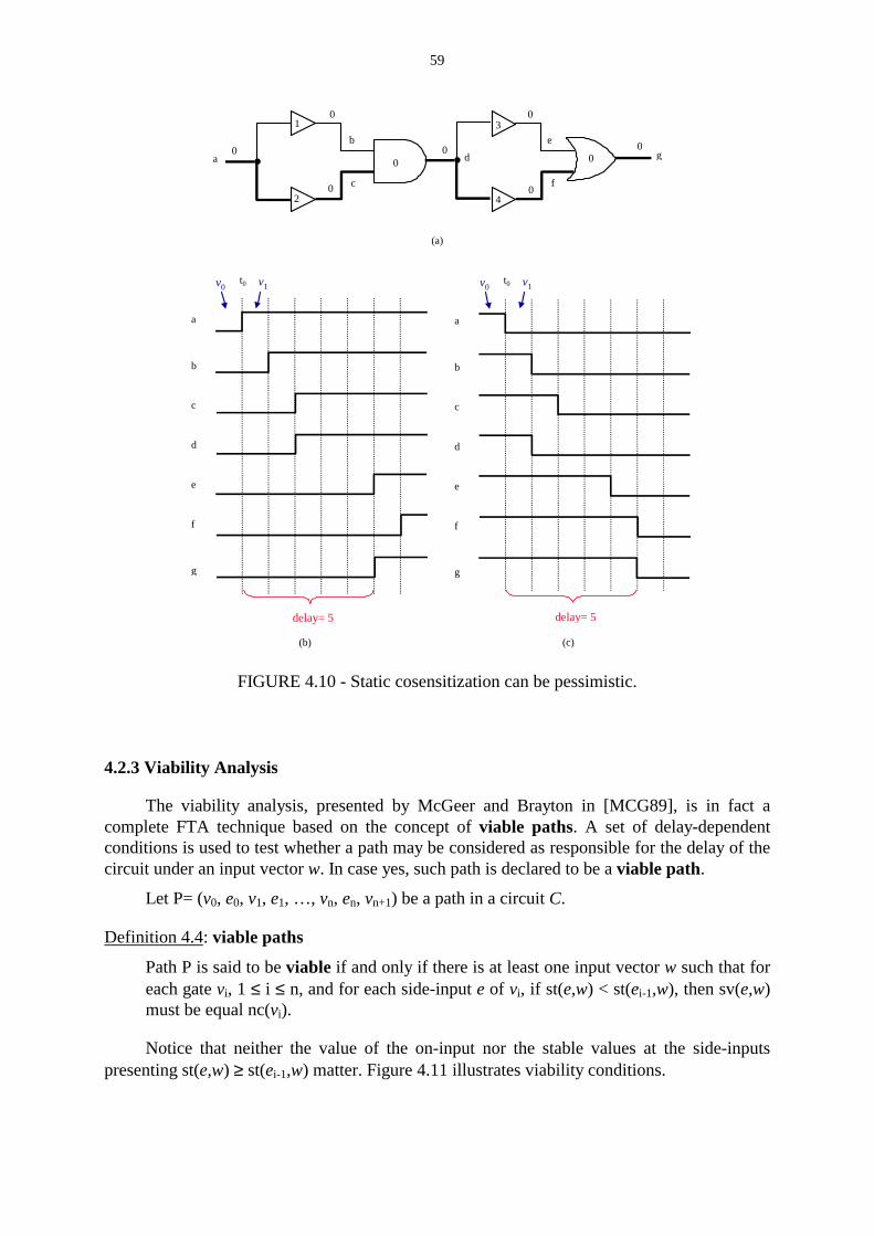
59
a0
1
0
2
0
4
g
30
0
0
0
0
0b
c
d
e
f
(a)
(b) (c)
a
b
c
d
e
f
g
delay= 5
t0v0 v1
a
b
c
d
e
f
g
t0v0 v1
delay= 5
FIGURE 4.10 - Static cosensitization can be pessimistic.
4.2.3 Viability Analysis
The viability analysis, presented by McGeer and Brayton in [MCG89], is in fact acomplete FTA technique based on the concept of viable paths. A set of delay-dependentconditions is used to test whether a path may be considered as responsible for the delay of thecircuit under an input vector w. In case yes, such path is declared to be a viable path.
Let P= (v0, e0, v1, e1, …, vn, en, vn+1) be a path in a circuit C.
Definition 4.4: viable paths
Path P is said to be viable if and only if there is at least one input vector w such that foreach gate vi, 1 ≤ i ≤ n, and for each side-input e of vi, if st(e,w) < st(ei-1,w), then sv(e,w)must be equal nc(vi).
Notice that neither the value of the on-input nor the stable values at the side-inputspresenting st(e,w) ≥ st(ei-1,w) matter. Figure 4.11 illustrates viability conditions.

60
t
nc
nc
c
vi
sideinputsof vi
FIGURE 4.11 - Conditions for path viability.
Viability, however, does not imply static cosensitization. A path may be declared viablewithout being statically cosensitizable, and thus, be false.
Consider the simple circuit of figure 4.12, taken from [CHE93], where all gates havedelay equal 1 except the inverter, which has zero delay. Consider also that each connectionhas zero delay. The path showed in bold is viable for input vector 1,0. This is because byapplying such vector the stable time at the AND gate inputs are equal, allowing us todisregard the stable value at the side-input to this gate. The same happens with respect to theOR gate (figure 4.12a). However, this path is not statically cosensitizable. For a=1, c=0 andthus d=0, which is the AND gate controlled value. But viability requires that a, being the on-input to the AND gate, must be at the AND gate noncontrolling value, i.e., a=0. Similarly, fora=0, d=0 and e=1. Again, the side-input (with respect to the OR gate) presents a controllingvalue while the on-input has the noncontrolling value (figure 4.12b). Hence, this path is notstatically cosensitizable.
(a)
a
b
c
d
e
f
1
1
1 (0) 1 (0)
0 (0)
0 (0)
0 (1)
0 (2)10
0 (1)
0 (0)
(b)
a
b
c
d
e
f
1
1
0 0
1
1
110
0
FIGURE 4.12 - Example of viable path (a) that is not statically cosensitizable (b).

61
As a theory, viability is remarkable because it presented the first set of conditionsinherently considering the monotone speedup. Indeed, it was demonstrated in [MCG91] thatviability is both robust and correct on networks composed of symmetric gates (although it isdefined on networks of complex gates, as will be detailed in chapter 5). However, it was notdemonstrated that viability is the exact delay estimate. Nevertheless, it is known that the delayvalue returned by viability is correct.
4.2.4 Exact Floating-Mode Sensitization
The two delay-independent sensitization conditions, static sensitization and staticcosensitization, are sufficient and necessary, respectively, for a path to be declared asresponsible for the delay of a circuit. However, the necessary and sufficient condition for apath to be responsible for the delay of a circuit under the floating mode is a delay-dependentcondition that is stronger than static cosensitization but weaker than static sensitization. It hasbeen introduced in [CHE91] and is currently referred to as the exact floating-modesensitization criterion.
Let P= (v0, e0, v1, e1, …, vn, en, vn+1) be a path in a circuit C.
Definition 4.5: exact floating-mode sensitization
Path P is said to be exactly sensitizable or true (under the floating mode) if and only ifthere is at least one input vector w such that for each gate vi along P, 1 ≤ i ≤ n, one of thefollowing conditions hold:
1. If sv(ei-1) = c(vi), then for each side-input e of vi , if sv(e) = c(vi), then st(e) ≥ st(ei-1)
2. If sv(ei-1) = nc(vi), then for each side-input e of vi, sv(e) = nc(vi) with st(e) ≤ st(ei-1)
In other words, for a path to be responsible for the delay of a circuit under the floatingmode it is necessary that, for each gate g along the path:
1. If the output of g is at the controlled value, then its on-input must present thecontrolling value of g and furthermore, has to have a stable value no greater than thestable values of the side-inputs having the controlling of g.
2. If the output of g is at the noncontrolled value, then its on-input has to have a stabletime no smaller than the stable times of all the side-inputs of g.
These conditions are depicted by figure 4.13.
Let us use these conditions to determine the delay of the previously studied circuits.Consider the circuit of figure 4.1a, reproduced in figure 4.14. Applying a vector a=1 sensitizesthe path of length 6 shown in bold. In the figure, each connection has both a logical value anda stable time value, the later in parenthesis. This result illustrates that the sensitizationcondition takes into account the monotone speedup property, unlike transition delaysimulation with fixed gate delays.

62
t
nc
nc
c
cvi
sideinputsof vi
nc
nc
t
nc
(a) (b)
FIGURE 4.13 - Conditions for exact floating-mode sensitization.
1 (0)a
12
2
2
1
2
2h
0 (2)
0 (1)
0 (4)
0 (4)
0 (6)
0 (3)
1 (2)
FIGURE 4.14 - First example of exact floating-mode sensitization.
Now consider the circuit of figure 4.5, reproduced in figure 4.15. Applying the vector000 gives a floating delay of 3, illustrating that the sensitization condition is weaker thanstatic sensitization. The paths (a,d,f,g) and (b,d,f,g) can be considered as responsible for thedelay of the circuit.
a
b
c
d
e
f
g
1
1
1
1
0 (0)
0 (0)
0 (0)1 (1)
0 (1)
0 (2)
0 (3)
FIGURE 4.15 - Second example of exact floating-mode sensitization.
Finally, consider the circuit of figure 4.7, reproduced in figure 4.16. Applying a=0sensitizes path (a,b,d,f,g) under the floating mode, while applying a=1 sensitizes path(a,c,d,e,g), also under the floating mode. As long as both paths have delay=5, the floatingdelay of this circuit is 5. This also shows that the exact floating-mode sensitization conditionis stronger than static cosensitization. Recall that static cosensitization reports a delay of 6 forthis circuit.

63
The previous considerations justify the true floating (single-vector) abstraction as anecessary and sufficient condition for a path to be responsible for the delay of a circuit underthe floating model.
(a)
a
1
0
2
0
4
g
3b
c
d
e
f
0 (0)0 (1)
0 (2)
0 (1)
0 (4)
0 (5)
0 (5)
(b)
a
1
0
2
0
4
g
3b
c
d
e
f
1 (0)1 (1)
1 (2)
1 (2)
1 (5)
1 (6)
1 (5)
FIGURE 4.16 - Third example of exact floating-mode sensitization.
Note that the conjunction of the single-vector delay model with the sensitizationconditions presented in definition 4.5 gives rise to a set of fundamental assumptions that areimplicitly assumed by any floating delay computation method. Such assumptions are shown infigure 4.17. Assume the AND gate of figure 4.17a has delay d and is embedded in a largercircuit, and a vector pair (v1,v2) is applied to the circuit inputs, resulting in a rising transitionoccurring at time t1 on the first input of the AND gate and a rising transition at time t2 on thesecond input. The output of the gate rises at a time given by max(t1,t2)+d. Under the floatingmode, only the values on v2 are considered. Thus, in this case, a 1 arrives at the first input at t1
and a 1 arrives at second input at t2. As a consequence, a 1 appears at the output at timemax(t1,t2)+d. Similarly, in the case of figure 4.17b, two falling transitions arrive at the ANDinputs at time t1 and t2, respectively, resulting in a falling transition at the output at timemin(t1,t2)+d. The abstraction under the floating mode considers a 0 arriving at the first input attime t1 and a 0 arriving at the second input at time t2. A 0 appears at the output at timemin(t1,t2)+d.
Now consider the situation of figure 4.17c, where a rising transition occurs at time t1 onthe first input of the AND gate and a falling transition occurs at time t2 on the second input.Depending on the arriving order of the transitions occurring at the gate inputs, the output mayeither stay at 0 (if t1≥t2) or glitch to 1 (if t1<t2). If circuit simulation were used, the occurrenceof a glitch would be easily detected. However, under the floating model only v2 is considered,as it is a single-vector approach. The 1 at the first input of the AND gate arrives at t1, and the0 at the second input arrives at t2. The output of the AND gate obviously settles to 0 on v2. Butthe problem is determining at what time this occurs: if t1≥t2, then the output is always 0, but ift1<t2, then the output becomes 0 only at t2+d. In order not to underestimate the critical delay ofa circuit, any sensitization condition for single-vector computation model have to assume thatthe noncontrolling value (the 1, in the case of AND gate) arrives before the controlling value(the 0, in the case of AND gate), or in other words, t1<t2. Under the floating mode thiscorresponds to assuming that the values on the previous vector v1 were noncontrolling.

64
(a)
(b)
(c)
max(t1,t2)+d
t1 d
t2
min(t1,t2)+d
t1 d
t2
t1 d
t2
t1+d t2+d
dmax(t1,t2)+d
1t1
t2
1
1
dt1
t2
0
0
min(t1,t2)+d
0
dt1
t2
0
1
t2+d
0
events assumptions
FIGURE 4.17 - Fundamental assumptions made in single-vector exact floating mode.
The rules illustrated in figure 4.17 represent a timed calculus for single-vectorsimulation with delay values that can be used to determine the exact floating mode delayunder an applied vector v2 (assuming pessimistic unknown values for v1) and the paths that areresponsible for the delay under v2. The rules can be generalized as follows:
1. If the gate output is at a controlled value, pick the minimum among the delays of thecontrolling values at the gate inputs. (Of course, there has to be at least one inputwith a controlling value. The noncontrolling values are ignored.) The delay at thegate output is obtained by adding the gate delay to the selected input delay.
2. If the gate output is at a noncontrolled value, pick the maximum of all the delays atthe gate inputs. (All the gate inputs have to settle at noncontrolling values.) Thedelay at the gate output is obtained by adding the gate delay to the selected inputdelay.
4.2.5 Other Sensitization Criteria
The former subsections presented the most important sensitization criteria. Obviously, anumber of other sensitization criteria exist, but all of them are in fact approximations of theexact floating-mode criterion. Examples of other criteria are the approximate criterion[CHE93] and the vigorous criterion [CHA93].
4.3 Qualitative Comparison Between Sensitization Criteria
It is worth to notice that the concept of path sensitizability is relative. Indeed, theaccuracy of delay estimates does not depend solely on the used sensitization criterion. It isimportant to recall that there is a set of delay computation models underlying any FTAalgorithm. Thus, the exact floating-mode sensitization criterion is just an upper bound on the

65
circuit delay, not only because it assumes the pairs of vector condition, but also because it hasto be (monotone speedup) robust.
At this point, it has to be mentioned that the customary terminology may cause someconfusion, since the delay computation models underlying path sensitization criteria are rarelymade clear. Let us consider the exact floating-mode criterion. Although it has been definedunder the floating mode, its original name was just “exact criterion”. In order to avoid anymisunderstanding that the term “exact” may cause, it has lately been referred to as exactfloating-mode criterion.
From section 2.1 it became clear that the topological delay is always an upper bound onthe delay of a circuit. However, it may be too pessimistic because the longest paths may befalse.
Although easy to implement, the static criterion is not adequate for furnishing a safedelay estimate because it may declare false a path that is true. Thus, it constitutes a lowerbound on the circuit delay. Considering the single vector delay model, the exact criterion andviability are safe delay estimates because they are guaranteed not to underestimate circuitdelay. Moreover, such criteria are currently the ones providing the tightest delay estimates.
Finally, the true delay of a circuit could be ideally obtained by using a delay calculationbased on delay by sequences of vectors. Unfortunately, no efficient implementation of input-independent technique using this model exists.
true delay(sequences of vectors)
topologicaldelay
staticsensitization
exact floatingand viability
unsafe estimate
tighter delay estimate
FIGURE 4.18 - Comparison between sensitization criteria.

66

67
5 Functional Timing Analysis Algorithms
The most representative sensitization criteria were presented and discussed in theprevious chapter. Although the sensitization criterion is a fundamental issue of a timinganalysis algorithm, it is not the only one. FTA algorithms may greatly differ by the delaycomputation procedure, which basically corresponds to the way path sensitizability is takeninto account for determining a circuit delay estimate.
This chapter discusses some of the most relevant delay computation algorithms. Itbegins by proposing a taxonomy that allows for classifying the existing FTA algorithmsaccording to two other aspects, different from the sensitization criterion:
• The number of paths simultaneously handled and
• The method used to determine whether the sensitization conditions are satisfiable ornot.
Section 5.1 presents a brief historical review of FTA algorithms. The mentionedalgorithms are classified following the proposed taxonomy.
Afterwards, three types of FTA algorithms are discussed in more detail: ATPG-basedsingle path sensitization, ATPG-based concurrent path sensitization and SAT-basedconcurrent path sensitization. For each type, a typical example of algorithm is detailed.
5.1 Classification of FTA Algorithms and Historical Review
Although many works on path sensitization criteria and FTA algorithms and techniqueshave been published in the last fifteen years, the absence of a standard taxonomy on thesesubjects represents a serious difficulty, mainly to those researchers debuting activities in thesefields. It is true, however, that some authors have been more cautious with the terminologyaspects. This seems to be the case of McGeer-Brayton’s works, Devadas’ and collaborators’works, and more recently, Ashar-Malik’s and Silva-Sakallah’s works.
Given the similarities between the functional timing analysis (FTA) problem and theautomatic test generation (ATPG) problem, it is obvious that many of existing solutions to thelatter are of interest for the former. Hence, while the two classes of problems may share anumber of basic algorithms, they also share a common terminology, which basic concepts arestated in chapter 3, and are further employed in the sequel.
Early FTA algorithms operated on a per-path basis, by using an adapted version of D-algorithm. This was the case of the works presented in [BEN87] (detailed in [BEN90]),[BRA88], [CHE91] and [CHE93]. In the two latter cases, not only static logic values wereasserted, but also the time these signals became stable was tracked. All of these algorithmsshared a common feature that was, only one path was considered at a time, concerning thesensitization tests. In practice, this corresponds to the ATPG concept of single pathsensitization!

68
But since early, it has been recognized that some circuits may exhibit hundreds ofthousands of false paths greater than the critical path [KEU91][DEV94][LAM94], renderingthe per-path operation impractical due to its prohibitive computational cost. On the otherhand, early ATPG algorithms had already the ability of dealing with multiple paths at a time,or in other words, were able to perform concurrent (or multiple) path sensitization. Notsurprisingly, some FTA solutions tried, and actually succeeded, to catch such ability. Amongthem, the most remarkable are the work of Devadas et al. [DEV91] [DEV93a], that of Silvaand Sakallah [SIL94] [SIL94a] and that of Ashar and Malik [ASH95]. Actually, thecontribution of the latter work concerns a circuit equivalent form allowing for usingunmodified ATPG algorithms to resolve the FTA problem. A mixed approach is alsoencountered in the literature [CHA93]. In this, a set of potential critical paths is identified byconcurrent path sensitization. Single path sensitization is then applied to this set to identify thecritical path.
Another issue, theoretically independent on the number of paths that an algorithm canhandle, is the method used to determine whether the sensitization conditions are satisfiable ornot. Recall all previously mentioned algorithms. The method they use to determine thesensitizability of paths (either operating on a single path or on multiple paths) relies onasserting logic values to some of the circuit nodes (on-inputs and side-inputs, in case of singlepath) and then, by implicating these values to other circuit nodes, watching whether anyinconsistency occurs or not. Such procedure has also been borrowed from classical ATPGalgorithms, thus being referred to as ATPG-based.
In 1989 McGeer and Brayton called the attention to the fact that the set of conditionsnecessary to declare a path as sensitizable (under a given criterion) could be formally stated asa path sensitization function [MCG89]. Hence, formal methods could be used to resolve thepath sensitization problem, instead of the traditional ATPG-based method. Their firstsolutions to this alternative formulation of the sensitization problem involved dynamicprogramming [MCG89] and BDDs [MCG91].
Naturally, it would be expected that the same type of formulation to be straightforwardapplicable to ATPG. In this case, however, the formalized set of conditions tends to presenthigher complexity since not only the propagation conditions must be taken into account, butalso the conditions for fault activation. The work incarnating this shift in terms of ATPGmethods is that of Larrabee [LAR92]. Larrabee used Boolean satisfiability to solve aformulation that expressed the Boolean difference between faulty and fault-free circuits.
This shift on methods came again to the FTA field by means of the so-called pathrecursive functions, defined by McGeer and Brayton in [MCG91a], which provided theformalization necessary to apply Boolean satisfiability algorithms. After that, satisfiability-based (or SAT-based) FTA has evolved. Some other SAT-based FTA techniques deservingcitation are [MCG93], [SIL93], [SIL96], [SIL98] and [SIL99].
Summarizing the taxonomy that was presented along with the historical review, theexisting solutions to the FTA problem may be classified according to the following issues:
• The path sensitization criterion used,
• The number of paths simultaneously handled and
• The method used to test path sensitizability.
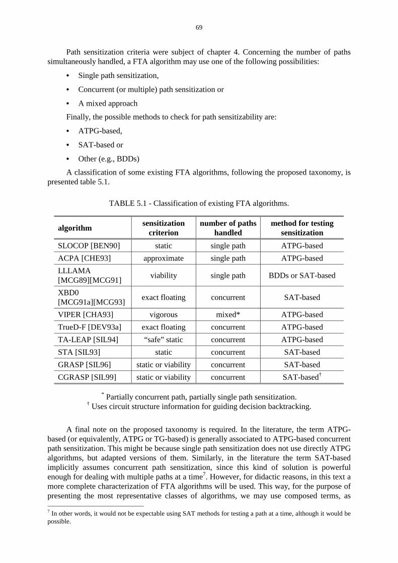
69
Path sensitization criteria were subject of chapter 4. Concerning the number of pathssimultaneously handled, a FTA algorithm may use one of the following possibilities:
• Single path sensitization,
• Concurrent (or multiple) path sensitization or
• A mixed approach
Finally, the possible methods to check for path sensitizability are:
• ATPG-based,
• SAT-based or
• Other (e.g., BDDs)
A classification of some existing FTA algorithms, following the proposed taxonomy, ispresented table 5.1.
TABLE 5.1 - Classification of existing FTA algorithms.
algorithmsensitization
criterionnumber of paths
handledmethod for testing
sensitization
SLOCOP [BEN90] static single path ATPG-based
ACPA [CHE93] approximate single path ATPG-based
LLLAMA[MCG89][MCG91]
viability single path BDDs or SAT-based
XBD0[MCG91a][MCG93]
exact floating concurrent SAT-based
VIPER [CHA93] vigorous mixed* ATPG-based
TrueD-F [DEV93a] exact floating concurrent ATPG-based
TA-LEAP [SIL94] “safe” static concurrent ATPG-based
STA [SIL93] static concurrent SAT-based
GRASP [SIL96] static or viability concurrent SAT-based
CGRASP [SIL99] static or viability concurrent SAT-based†
* Partially concurrent path, partially single path sensitization.† Uses circuit structure information for guiding decision backtracking.
A final note on the proposed taxonomy is required. In the literature, the term ATPG-based (or equivalently, ATPG or TG-based) is generally associated to ATPG-based concurrentpath sensitization. This might be because single path sensitization does not use directly ATPGalgorithms, but adapted versions of them. Similarly, in the literature the term SAT-basedimplicitly assumes concurrent path sensitization, since this kind of solution is powerfulenough for dealing with multiple paths at a time7. However, for didactic reasons, in this text amore complete characterization of FTA algorithms will be used. This way, for the purpose ofpresenting the most representative classes of algorithms, we may use composed terms, as 7 In other words, it would not be expectable using SAT methods for testing a path at a time, although it would bepossible.

70
ATPG-based single path sensitization, ATPG-based concurrent path sensitization and SAT-based concurrent path sensitization. These types of algorithms are detailed in the followingthree sections.
Before beginning the discussions on FTA algorithms, it is worth to mention that anyFTA algorithm presents three basic steps that can be presented as:
1. Circuit graph creation
2. Graph pre-processing, to compute maximal delays
3. Circuit delay computation
Thus, different types of algorithms differ from each other by the third step. This step canindeed be further divided in other substeps that may greatly differ, according to the proposedclassification. These differences will be focused in the next sections.
5.2 ATPG-Based Single Path Sensitization Algorithms
ATPG-Based single path sensitization algorithms check the sensitization conditionsof a given path by asserting logic values to on-inputs and side-inputs and implicating thesevalues to other circuit nodes, in a D-algorithm-like fashion. Indeed, such technique tends to beless complex than the D-algorithm because only the propagation phase is of interest.Moreover, only single path sensitization is tried.
In order to guarantee that the critical path delay is found, the algorithm must begin byexamining the topologically longest path. If the sensitization conditions are satisfied, suchpath is assumed to be the one responsible for the circuit critical delay and its delay is assumedto be the circuit critical delay. Otherwise, the next topologically longest path must be tracedand checked. The procedure continues until a sensitizable path is found.
Single path sensitization algorithms (sometimes called per-path algorithms) share acommon problem that is tracing paths according to a non-increasing order of their delays. Themost efficient algorithms to accomplish this, referred to as path enumeration algorithms, areof complexity O(n log n), with n equals the number of graph nodes [PIN98]. The proceduremay be speeded up slightly if the sensitizability check is accomplished while the path is beingtraced. In this case, the steps for testing sensitizability would be basically the same as in theD-algorithm: implication and justification [ROT66]. For each new gate appended to the pathbeing traced, logic values are asserted to the side-inputs. Then, these values are propagatedbackward to the primary inputs and forward to the primary outputs. In the case of delay-dependent sensitization conditions, the stable time of these values are also taken into account.Non-evaluated nodes remain with don’t care values. Figure 5.1 depicts the execution of such asingle path sensitization procedure.
While justifying a given set of propagation conditions at a gate, more than one set ofpossible logic values may exist for the nodes within the logic cone arriving to the consideredgate. These possible sets are stored in a list for future evaluation, in case any inconsistencyoccurs while evaluating the propagation conditions at the next gates of the path. If there existat least one assignment of logic values to the circuit nodes satisfying to the sensitizationconditions, then the path is declared sensitizable (with respect to the applied sensitizationcondition and delay models). On the other hand, a path cannot be declared unsensitizable untilall possible assignments of logical values have been tested.

71
0 (0)
1 (td1)
X (?)
X (0)
X (?)
X (?) X (?)
X (?)
X (?)
X (?)
D-frontier
forward implication
backward implication
FIGURE 5.1 - Single path sensitization procedure.
In order to speedup execution time, some ATPG-based single path sensitizationalgorithms (as [DU89] and [CHE93]) do not perform the justification step, since most falsepaths may be detected in the implication step. However, the implication step is not able toidentify all sensitizable paths [PES94] and thus, when justification is not performed, anunsensitizable path may be declared sensitizable, resulting in an overestimation of the circuitdelay.
As mentioned earlier, one important issue in single path sensitization algorithms is thepath enumeration algorithm itself. The problem of tracing paths of a combinational circuithas been studied since the 80’s, when various path enumeration algorithms were proposed.Some of them were direct implementations of the classical Breadth-First Search (BFS) andDepth-First Search (DFS) graph traversal procedures (e.g., those presented in [YEN88]).However, as long as these algorithms do not consider pre-processed graph information,tracing paths in an arbitrary order of depth, they were not efficient for enumerating circuitpaths in a non-increasing order of lengths (i.e., path delays). Other algorithms applied pruningheuristics based on designer’s knowledge of the circuit, as those in [OUS85]. However, themost efficient algorithms are those based on the Best-First Search procedure [WIS84], as theones presented in [YEN89] and [YEN91] (and generalized in [MCG91]), and thus will befurther discussed in the following subsections.
5.2.1 The Best-First Search Path Enumeration Procedure of Yen et al. [YEN89]
The best-first search algorithm, also called A* [WIS84], is an algorithm that decides thesearch trajectory based on pre-computed path lengths. The main reason for using suchalgorithm for path enumeration of combinational circuits is that it allows for a continuous andorganized exploration of the search space with time complexity O(nlogn) [MCG91].
The best-first search procedure implemented by Yen et al. [YEN89] assumes a singledelay per gate and can be divided into three main phases:
1. circuit graph creation
2. graph pre-processing phase
3. path enumeration phase.

72
In the first phase, a DAG is created to represent the circuit under analysis. In this DAG,each CMOS gate is represented by a node and each connection, by an edge. Dummy nodes(i.e., with zero delay) are added to represent primary inputs and primary outputs. A sourcenode s and a terminal node t are also created; a dummy edge is added between node s andeach primary input node and between each primary output node and node t. With thiscanonical DAG representation, any circuit path assumes the form P = ( v0, v1, v2, v3, ...vn, vn+1
), where vn is a graph node. If v0 = s and vn+1 = t, then P is said to be a complete path. If v0 ≠ sor vn+1 ≠ t , then P is said to be a partial path. Figure 5.2 shows the DAG for the circuit offigure 2.1. For the sake of simplicity, consider that the delay of connections is lumped atcircuit nodes, i.e., the delay represented by a given net is assigned at its fanin node.
An important aspect that must be considered in the implementation of path enumerationalgorithms is the adopted gate delay computation model. That is, the enumeration algorithmmust take into account whether a single delay or a pair of delays is assigned to each circuitgate. By pair of delays it is meant separate fall and rise delays and thus, the polarity of signalsmust be considered in the calculation of path delays.
199,261
NAND3a
b
c
d
s
237,284
NAND5
173,206
NAND6
129,181
NAND4
47,247
NOR0
47,115
INV1
118,158
118,158
NAND7
173,206
0,0
0,0
0,0
0,0
0,0
292,362
z tNAND1
0,0 0,0
0,0 0,000
292,362362
44,91
INV0
406,383453
NAND0
480,450520
NAND2
501,564611
611,748858
579,661701
763,762872
809,878987
1051,10151193
921,8171064
999,10471156
1047,9991156
1047,9991156
1015,10511193
1015,10511193
1051,10471193
Notation
tdhl = fall delay of the gate
tdlh = rise delay of the gate
mdtf = maximal delay to t for falling transition
mdtr = maximal delay to t for rising transition
mdtf,mdtr
tdhl,tdlh
mdt
FIGURE 5.2 - DAG for circuit of figure 2.1, pre-processed according to the best-first searchprocedure.
In the simpler case, when a single delay is assigned to each circuit gate, the delay of apath is computed just by adding the delay of each gate of the path. Signal polarity isdisregarded. For a partial path P = ( Q, vn+1 ), with Q = ( s, v1, v2, v3, ...vn ) the delay iscalculated by:
)td(d(Q)d(P) 1+nv+= (5.1)
where td(vn+1) is the delay of gate vn+1 appended to partial path Q.
For ordering path tracing, the best-first procedure of Yen et al. [YEN89] goes through apre-processing phase in which the maximal delay to node t (mdt) is calculated for each nodeand stored in the data structure. The mdt(v) is defined as the maximum of the delays of allpossible partial paths starting at node v and ending at node t and is calculated by the formula:
)maxmdt()d()mdt( iuvv += (5.2)

73
where ui ∈ adj(v) (i.e., the list of successors of node v). The procedure for calculating themdts of all nodes in the graph starts at node t and goes backwards in a breadth-first order. Anode v will have its mdt computed only after all of its successors’ mdts have been computed.The procedure ends when node s has its mdt calculated. At the same time the mdt of a node vis calculated, its list of successors, adj(v), is sorted in a non-increasing order of eachsuccessor’s mdt. In the graph of figure 5.2 the value used as gate delay for calculating mdt(v)is maxtdlh(v),tdhl(v).
The mdt is a valuable information, which allows to avoid searching branches that willnot result in paths having greater delay than the smallest delay among the paths alreadydiscovered. It also permits to keep the partial paths candidates ordered according to theiresperances. The esperance of a partial path P = ( v0, v1, v2, v3, ...vi, vi+1 ), obtained by appendingnode vi+1 to the partial path Q = ( v0, v1, v2, v3, ...vi ), is the maximum delay of all completepaths that have Q as a prefix [BEN87] and is calculated by:
)mdt(d(Q)e(P) 1+nv+= (5.3)
In the path enumeration phase the k most critical paths are found and stored in a linearstructure named k-list, in a non-increasing order of their delays. Each position of k-list stores agiven path P (initially, a partial path, but at the end of the procedure, a complete path), itsdelay, d(P), and its esperance, e(P). At the beginning of the procedure, the first ds partial pathsmade up of node s and each of its successors will be stored in the first ds positions of k-list,with ds being the outdegree of node s. If ds > k, then only the first k partial paths will be kept(k is a user provided value). Once k-list is initialized with the first partial paths, a functioncalled extend_and_replace is invoked for each partial path of k-list, beginning from the firstposition, k-list[0]. This function takes the partial path stored in k-list[i] and extends it untilnode t has been reached. Suppose that v is the last node of partial path P = ( v0, v1, v2, v3, ...v ),stored at k-list[i], which is to be extended, and adj(v) = u0, u1, u2, u3, ... is its ordered list ofsuccessors. Extending P through u0 originates a new partial path P0 , with the same esperanceof P (because u0 is the first successor of v). Thus, P0 will replace P in position k-list[i].However, extending P through node u1 creates a new partial path P1 with esperance
)mdt(d(P))e(P 11 u+= . Similarly, extending P through node u2 creates a new partial path P2
with esperance )mdt(d(P))e(P 22 u+= and so on. Before extending path P by appending nodeu0, each “side” partial path except P0 has its esperance calculated in order to know whetherthis new partial path will be inserted in k-list or not. If the new partial path’s esperance isgreater than the esperance of the partial path stored in k-list[k-1] (i.e., the last position of k-list), then it is inserted in an ordered manner. Otherwise, neither this partial path nor the nextside partial paths will be inserted because partial paths are examined in the same order of theelements in adj(v). This results in a prune of the search space. In case a new side partial pathis to be inserted, the insertion position j will be within the range ( i < j ≤ k-1 ) and the pathstored in position k-list[k-1] will be automatically discarded. Each new partial path Pi that isinserted in k-list will have its delay calculated by:
)d(d(P))d(P ii u+= (5.4)
Once path P, stored in k-list[i], is completely extended, d(P) = e(P) because it is acomplete path. Then, function extend_and_replace will be called for the partial path storedin k-list[i+1]. The path enumeration phase will end when the partial path stored in k-list[k-1]is completely extended. At this point, k-list holds the k-most critical paths of the circuit.Figure 5.3 shows the contents of k-list after its initialization, for the circuit represented by thegraph of figure 5.2.

74
It is interesting to note that while the path stored in k-list[i] is being extended it is notpossible to precise which will be the next partial path to be extended. On the other hand, oncepath of k-list[i] has been completely extended, the next path to be extended is the one storedin k-list[i+1]. This systematic search of the space of possibilities is responsible for the greatestadvantages of the best-first procedure over the depth-first procedure [YEN89][MCG91]: pathsare traced in a non-increasing order of their delays with no need for costly backtracks.
d e path
0
0
0
0
0
0
1193
1193
1156
1156
0
0
0
1
2
3
k-1
i
s
s
s
c \
d \s
b \
a \
\
\
FIGURE 5.3 - k-list structure initialized with the first partial paths of the circuit of figure 5.2.
5.2.2 Best-First Search Path Enumeration Considering Different Fall and Rise GateDelays
This section describes the modifications to the basic best-first search of Yen et al.needed for dealing with separate fall and rise gate delays. Although of maximal interest forimplementing useful FTA algorithms, such modified best-first procedure is described in detailonly in [GÜN98], [GÜN98b] and [GÜN99]. The basic idea is to store two lists of successorsat each graph node: one for the falling transition and another for the rising transition at thenode’s output. This also implies in calculating two mdts, as will be explained in the sequel.Many of the ideas described here may also be applied in the context of ATPG-basedconcurrent path sensitization algorithms.
In order to consider different fall and rise gate delays, each topological path isdecomposed into two distinct logical paths by fixing the type of the transition taking place atits primary input. Thus, the delay of a partial logical path P = ( Q, vn+1 ), with Q = ( s, v1, v2,v3, ...vn ) is calculated by:
)tdhl(d(Q)d(P) 1+nv+= (5.5)
if the input of vn+1 is undergoing a rising transition and
)tdlh(d(Q)d(P) 1+nv+= (5.6)
if the input of vn+1 is undergoing a falling transition. By considering signal polarity, thesecalculations are implicitly adding some primitive information on the relationship between thegates of a path.
In the pre-processing phase, the procedure for calculating the mdts of all nodes isessentially the same, except that for each node two values of mdts must be calculated: mdtfand mdtr. For a given node v, mdtf(v) and mdtr(v) give the maximum of the delays of allpossible partial logical paths starting at node v and ending at node t, for a falling transitionand for a rising transition at the output of v, respectively, and are calculated by:

75
)maxmdtr()tdhl()mdtf( iuvv += (5.7)
)maxmdtf()tdlh()mdtr( iwvv += (5.8)
with ui ∈ adjf(v) (the list of successors of v for a falling transition) and wi ∈ adjr(v) (the listof successors of v for a rising transition).
Hence, each node v has two lists of successors, adjf(v) and adjr(v), sorted in a non-increasing order of each successor’s mdtf and mdtr, respectively.
Similarly, the esperance of a partial logical path P = ( Q, vn+1 ), obtained by appendingnode vn+1 to the partial logical path Q = ( s, v1, v2, v3, ...vn ), is calculated by:
)mdtf(d(Q)e(P) 1+nv+= (5.9)
if the input of vn+1 is undergoing a rising transition and
)mdtr(d(Q)e(P) 1+nv+= (5.10)
if the input of vn+1 is undergoing a falling transition. Figure 5.2 also shows the pre-processedmdtf and mdtr values for the DAG that represents the circuit of figure 2.1.
For determining the transition type at the end of a (partial) logical path two fields havebeen added to each position of structure k-list: type, which tells the transition type applied tothe path input, and level, which indicates the number of nodes that compose the current stored(partial) logical path.
The enumeration phase begins by storing the first 2ds partial logical paths made up fromnode s and its successors from adjf(s) or from adjr(s), with ds being the outdegree of node s.The nodes taken from adjf(s) and adjr(s) are chosen following a unique order. If 2ds > k, thenonly the first k partial paths will be kept. A modified version of extend_and_replace functionis then called for each partial path, beginning from the path stored in k-list[0]. This newversion is essentially the same as the original one, except that it deals with logical paths ratherthan topological paths. When partial logical path P = ( v0, v1, v2, v3, ...v ), stored in position k-list[i] is to be extended, the information of k-list[i].type and k-list[i].level is used to choosebetween adjf(v) and adjr(v) and to calculate the esperances and the path delays of eachextended path. Figure 5.4 shows the contents of k-list when the modified procedure isextending the most critical path of circuit example.
d e path
173
0
0
00
0
1051
1051
1047
1047
1015
999
\
0 1015
s c \
s b \
s a \
s d NAND7 \
0
0
0
999
0
0 \
0 0 \
type
k-1
0
1
2
3
4
...
5
6
7
8
1
0
0
0
0
1
1
1
s c \
s c \
s c \
s c \
FIGURE 5.4 - k-list structure for the best-first procedure that considers separate fall and risedelays.

76
It is important to remark that the proposed solution for dealing with separate fall andrise delays does not imply duplication of graph nodes, as does the solution presented in[LI89]. Instead, different fall and rise delays are considered by keeping track of the transitiontype along paths in order to choose a node’s next successor from either adjf or adjr.
Appendix 2 presents a study on the performance of best-first search-based pathenumeration procedures gathered from the following publications: [GÜN98a], [GÜN98b],[PIN98], [GÜN99] and [GÜN99a]. This study considers the gate delay model (single gatedelay or separate fall and rise gate delays) and also the type of data structure used for storingpartial paths (linear dynamic list or binary tree).
5.3 ATPG-Based Concurrent Path Sensitization Algorithms
Searching for a vector v2 that satisfies sensitization conditions for a particular path cantake 0(2n) time, with n being the number of primary inputs of the circuit. If this search is to beperformed on one path at a time, as single path sensitization algorithms do, then the executiontime is multiplied by the number of unsensitizable long paths that will be analyzed before thefirst sensitizable one is found. Furthermore, the time complexity of the fastest pathenumeration algorithms is O(n log n), where n is the number of nodes in the circuit graph[PIN98]. All these problems prevent single path sensitization to be used in FTA of largecircuits.
An alternate strategy is to directly answer the question of what the true critical delay ofthe circuit is and operate on sets of paths rather than a single path at a time [DEV93a]. Thequestion stated is: Is the delay of the circuit greater than or equal to δ? The value δ caninitially be set as the delay of the topologically longest path of the circuit and then beprogressively decreased while the answer to the question is “yes”.
A straightforward 0(2n) algorithm to find the true critical delay of a circuit that does notrequire explicit path enumeration is to simulate each of the 2n input vectors or minterms usingthe timed calculus and determine the longest delay seen at the circuit output. This process canbe speed up by using cube simulation instead of using minterm simulation. This can beaccomplished by using a modified version of the PODEM algorithm [GOE81], as proposed in[DEV93a].
In the next subsection the basic PODEM algorithm is described. Subsections 5.3.2, 5.3.3and 5.3.4 describe the modifications to the PODEM algorithm proposed in [DEV93a] toperform a timed cube calculus.
5.3.1 The PODEM Algorithm
PODEM [GOE81] is an enumeration algorithm that implicitly and exhaustivelyenumerates the input space using cubes rather than minterms, while trying to satisfy a givenobjective. The following explanation is oriented to a timing analysis implementation and wastaken from [DEV94], with modifications.
The topmost call of the procedure PODEM is described by the pseudocode in figure 5.5: itsimply inserts the given primary output line po on a justification list jlist with valuelvalue, and calls a search procedure SEARCH_1. lvalue is the logical value (either 0 or 1) to

77
be justified. Let us assume that a given logical value out_value (either 0 or 1) is to be justifiedat output po1 of a circuit. Thus, for the first call of the PODEM procedure, po←po1 andlvalue←out_value. This can be seen as detecting an (out_value) stuck-at fault at output po1of the circuit.
PODEM(po,lvalue)
jlist = po with logical value lvalue;
status = SEARCH_1(jlist); return(status);
FIGURE 5.5 - Pseudocode for the topmost call of the PODEM algorithm.
The search procedures are described by the pseudocodes of figures 5.6 and 5.7. Theprocedure SEARCH_1 calls a BACKTRACE procedure to find a primary input whose logical valueis currently unknown, beginning from the primary output po. The primary input is (initially)set to logical value 1 and the IMPLY procedure is called. This procedure in PODEMcorresponds to standard three-valued cube simulation (i.e., without any delay information).The implication procedure may produce a logical conflict. If no conflict occurs, SEARCH_1 iscalled recursively. The procedure terminates successfully in SEARCH_1 if the justification listis empty. In the case a logical conflict occurs in SEARCH_1 the algorithm backtracks to themost recent primary input assignment. The primary input is set to the logical value 0, and theSEARCH_2 procedure shown in figure 5.7 is called. Failure results if either the backtraceprocedure is unable to find a primary input to set or if the space has been completelyenumerated without success in SEARCH_2. In the case of conflict or failure, the network mustbe restored to the state it was immediately prior to the primary input setting that caused thefailure.
SEARCH_1(jlist) if(length of jlist is zero) return SUCCEED;
if(BACKTRACE(po,po_value,&pi,&pi_value) == FALSE) return(FAILED);
if(IMPLY(pi,pi_value,jlist) != IMPLY_CONFLICT)search_status = SEARCH_1(jlist);if(search_status) == FAILED) restore the state of the network to what it was prior to the most recent primary input assignment; search_status = SEARCH_2(jlist,pi,1-pi_value);
else restore the state of the network; search_status = SEARCH_2(jlist,pi,1-pi_value); return(search_status);
FIGURE 5.6 - Pseudocode for the first search procedure.

78
SEARCH_2(jlist,pi,pi_value)
backtracks = backtracks + 1 ; if(backtracks > BACKTRACK_LIMIT) return(ABORTED); if(IMPLY(pi,pi_value,jlist) != IMPLY_CONFLICT) search_status = SEARCH_1(jlist); if(search_status == FAILED)
restore the state of the network; else
search_status = FAILED; restore the state of the network;
return(search_status);
FIGURE 5.7 - Pseudocode for the second search procedure.
In order to illustrate the PODEM algorithm, consider the following situation: we need tofind an input vector that sets the output of the circuit of figure 5.8 to 1. As a first step, thePODEM algorithm sets all primary inputs to 2 (a=2, b=2 and c=2), which will represent theunknown value. The simulation or implication of these input values results in a 2 on all wiresincluding g, the output. Backtracing sets input a to 1. Implication immediately sets the g to 0as shown in figure 5.8a. The value of 0 at the output corresponds to a conflict since it wasasked for justifying a 1 at the output. Thus, it is necessary to backtrack to the most recentprimary input setting and change it. In this case a was set to 0. The output remains at 2 for thevector a=0, b=2 and c=2. Then, it is necessary to backtrace to another primary input b and setit to 1. Implication sets the output to 0 as illustrated in figure 5.8b, and we again have aconflict. The conflict results in backtracking to the most recently set primary input, in thiscase b. The input value is changed to 0. The vector a=0, b=0, c=2 results in an output of 2 asshown in figure 5.8c. Setting the remaining unknown input c to 1 sets the output to therequired value of 1, as shown in figure 5.8d. The search procedure ends in success.
The sequence of decisions taken in the previous example may be represented in terms ofa decision tree as the one shown in figure 5.9. The nodes of the tree correspond to primaryinputs, and the left and right edges from each node correspond to input settings of 1 and 0,respectively. The leaves of the tree correspond to primary output settings.
5.3.2 Cube Simulation
In order to use the PODEM algorithm for delay computation, we are interested inarriving at a timed calculus over three logical values, 0, 1 and 2 (unknown), that has thefollowing properties [DEV94]:
• It is equivalent to the timed calculus for computing the floating delay presented insubsection 4.2.4, in the case where inputs are completely specified;
• Given an incompletely specified vector, it produces an upper bound on theachievable delay over any of the minterms in the vector;
• Given an incompletely specified vector, it produces a lower bound on the achievabledelay over any of the minterms in the vector;
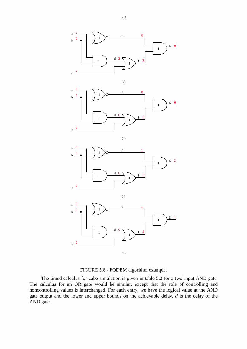
79
a
b
c
d
e
f
g
1
1
1
1
00
1
2
0 2
0
(b)
a
b
c
d
e
f
g
1
1
1
1
10
2
2
22
0
(a)
a
b
c
d
e
f
g
1
1
1
1
01
0
1
0 1
1
(d)
a
b
c
d
e
f
g
1
1
1
1
01
0
2
0 2
2
(c)
FIGURE 5.8 - PODEM algorithm example.
The timed calculus for cube simulation is given in table 5.2 for a two-input AND gate.The calculus for an OR gate would be similar, except that the role of controlling andnoncontrolling values is interchanged. For each entry, we have the logical value at the ANDgate output and the lower and upper bounds on the achievable delay. d is the delay of theAND gate.

80
01
a
0
b
c
1
0
1
1
FIGURE 5.9 - Binary decision tree for PODEM algorithm.
TABLE 5.2 - Timed calculus with unknown values.
i1
i20 1 2
0
0MIN(l1,l2)+d
MIN(u1,u2)+d
0l2+du2+d
0MIN(l1,l2)+d
u2+d
1
0l1+du1+d
1MAX(l1,l2)+d
MAX(u1,u2)+d
2l1+d
MAX(u1,u2)+d
2
0MIN(l1,l2)+d
u1+d
2l2+d
MAX(u1,u2)+d
2MIN(l1,l2)+d
MAX(u1,u2)+d
Each input of the AND gate has an associated logical value in 0,1,2 and a lower andupper bounds on the delay corresponding to the value. For input i1, for instance, the lowerbound is l1 and the upper bound is u1. The logical values in the table correspond to standardthree-valued simulation with 0, 1 and 2 values. To illustrate the process, it will be explainedthe calculation of the lower and upper bounds.
When the inputs are at 0,1, the rules of figure 4.17 are obeyed. When we have two 0sat the AND gate inputs, we choose the minimum of the lower (upper) bounds to calculate thelower (upper) bound at the output. When we have two 1s, we choose the maximum of lower(upper) bounds to calculate the lower (upper) bound at the output. When we have a 0 and a 1,we simply use the lower and the upper bounds of the 0 input.
When a 2 is at the input of an AND gate, the calculus gives the lower and upper boundson the achievable delay with either (0 or 1) setting of the 2 value. For example, consider theentry in the table when i1 is 1 and i2 is 2. The logical value at the AND output is 2. If i2 is setto 0, the lower (upper) bound on the delay will be l2+d (u2+d). However, if i2 is set to 1, thelower (upper) bound on the delay will be MAX(l1,l2)+d ( MAX(u1,u2)+d ). Sincel2≤MAX(l1,l2), l2 represents the lower bound on the achievable delay, and sinceMAX(u1,u2)≥u2, MAX(u1,u2) represents the upper bound on the achievable delay.

81
Now consider the situation where i1 is 0 and i2 is 2. In this case the value and the upperbound of i1 are passed through to the output. If i2 is set to 1, its delay will not matter. If i1 isset to 0, then the delay at the output will be MIN(u1,u2)+d. However u1≥MIN(u1,u2), and thuswe take u1+d. By the same reasoning, the lower bound will be MIN(l1,l2)+d.
When both inputs of the AND gate are 2, the lower bound on the achievable delay at theoutput is clearly MIN(l1,l2)+d. The upper bound on the achievable delay at the output isMAX(u1,u2)+d. Similarly, for the other entries.
Figure 5.10 illustrates the cube simulation using timed calculus. Each wire has a logicalvalue and two delay values. For example, 0(1,2) implies that the logical value of the wire is 0,the lower bound on the achievable delay is 1 and the upper bound on the achievable delay is 2.In figure 5.10a we have a vector with two 2 entries being simulated on the circuit. The outputof the circuit is 2, and for the minterms that are contained in 00210, the maximum achievabledelay is 4. When c is set to 1, the maximum achievable delay at the output is reduced to 3.
It is important to emphasize that the computed delays using the timed calculus merelygive the range of the achievable delays over all the minterms contained in the partial inputsetting (input cube). Even if a wire is at a known value under a partial input setting v, thedelay of the wire may be a range rather than a constant. For instance, consider the case wherethe first input of a two-input AND gate with zero delay is at 0 with l1= u1=4. If the secondinput is at 2 with l2= u2=3, then the lower bound on the output is achieved when the secondinput is set to 0; we obtain a delay of 3 at the output. The upper bound of 4 is achieved whenthe second input is set to 1. The output of the AND gate is 0 for both cases.
(b)
a
b
c
d
e
f1
11g h
1
1 out
0(0,0)
0(0,0)
1(0,0)
0(1,1)1(1,1)
1(0,0)
2(0,0)
0(2,2)2(2,3)
2(1,1)i
(a)
a
b
c
d
e
f1
11g h
1
1 out
0(0,0)
0(0,0)
2(0,0)
0(1,1)2(1,2)
1(0,0)
2(0,0)
2(2,3)2(2,4)
2(1,1)i
FIGURE 5.10 - Cube simulation using timed calculus.
5.3.3 Timed Test Generation
The application of the PODEM algorithm to compute the floating delay is described inthe sequel. In order to use the PODEM algorithm for computing the floating delay, the timed

82
calculus of table 5.2 must be used. It will be necessary to justify both logical values on wiresand delay values, and therefore the procedure is called timed test generation [DEV93].
The procedure is given a logical value L ∈ 0,1 and a number δ, and asked to find aninput vector, if such a vector exists, which sets the output of the circuit to L and which resultsin a floating mode delay ≥δ.
The procedure follows the same steps as the PODEM algorithm. However, there aresome important differences. The implication procedure uses the timed calculus of table 5.2rather than a purely logical calculus. Conflicts occurring during implication may be logicalconflicts or time conflicts. Logical conflicts as before correspond to the case when the outputis set to the value L. A time conflict occurs when the output is set to L but the upper bound onthe delay at the output is strictly less than δ. In this case too we have to backtrack since wecannot find an input vector within the cube corresponding to the current settings of theprimary inputs that has a delay ≥δ. The procedure ends successfully if the output has been setto L and the lower bound on the computed delay at the output is≥δ.
Consider the example of figure 5.11. The delay of each gate is assigned inside the gate.We wish to justify a 1(3) at the output of the circuit. Initially, all inputs are set to 2 with delayzero. Implication results in a 2 logical value at the output with a delay range (2,3) as shown infigure 5.11a. Backtracking sets a to 1. Implication immediately sets the output to 0, which is alogical conflict. We backtrack to the most recently set primary input and change its value.Hence, a is set to 0. Implication results in a 2 at the output with a delay range of (2,3).Backtrack sets b to 1, resulting in a 0 at the output, a logical conflict, as shown in figure5.11b. We backtrack to set b to 0. The output is unknown with the input setting correspondingto a=0, b=0 and c=2. Setting c to 1 results in the output being set to 1, but with a delay of(2,2), as shown in figure 5.11c. This is a time conflict since the upper bound on the delay isstrictly less than the required delay. Finally, setting c to 0 results in a 0 at the output, a logicalconflict, as shown in figure 5.11d. We have failed to find an input vector that results in a 1 atthe output of the given circuit with floating mode delay 3. Note that we did not have tosimulate all of the 23 different input minterms.
It is possible to find an input vector that results in a delay of 3 that produces a 0 at theoutput, as shown in figure 5.11d.
5.3.4 Backtrace
In PODEM the backtrace procedure is called when the primary output of the circuit is atan unknown value for the current primary input settings. It begins from the primary output ofthe circuit and traces back through the gates in the circuit to a primary input that is still at theunknown value. All gates traversed exhibit the property that their outputs are at unknownvalues. The required value at the output may dictate the required value at these gates, but ingeneral there will be choices as to which path the backtrace follows. The backtrace procedureuses heuristics in following paths that begin from a primary input with an unknown valuewhich when set will likely set the output to the desired value. The particular value that theprimary input is set to, either 0 or 1, is also decided heuristically.
The backtrace procedure in timed test generation is similar to the purely logicalbacktrace of PODEM except that it uses both the logical and the desired delay value at theoutput to choose what path to follow. The backtrace procedure is called when the primaryoutput is at the value 2, or if the lower and upper bounds on the computed delay at the output

83
are not equal. This is illustrated in figure 5.12, where we have a fragment of a circuit with apartial setting of its primary inputs. The logical value and the upper bound on the delay valuefor each wire is shown in the figure. The desired value at the primary output is 1(10) and isshown in bold. The current value of the output is unknown with an upper bound on the delaybeing 11.
a
b
c
d
e
f
g
1
1
1
1
2(0,0)2(1,1)
2(0,0)
2(0,0)
2(1,1)
2(1,2)
2(2,3)
(a)
a
b
c
d
e
f
g
1
1
1
1
0(0,0)0(1,1)
1(0,0)
2(0,0)
0(1,1)
2(1,2)
0(2,2)
(b)
a
b
c
d
e
f
g
1
1
1
1
0(0,0)1(1,1)
0(0,0)
1(0,0)
0(1,1)
1(1,1)
1(2,2)
(c)
a
b
c
d
e
f
g
1
1
1
1
0(0,0)1(1,1)
0(0,0)
0(0,0)
0(1,1)
0(2,2)
0(3,3)
(d)
FIGURE 5.11 - Timed test generation example.
Backtracing begins at the OR gate connected to the primary output. Since we require a 1at the primary output and the other two inputs to the OR gate are 0, we can infer that werequire a 1 at the first input to the OR gate. Furthermore, the delay value required is 9. Wenow move to the AND gate and note that we require a 1(9) at this output (in bold in the
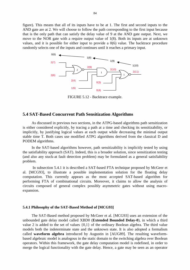
84
figure). This means that all of its inputs have to be at 1. The first and second inputs to theAND gate are at 2. We will choose to follow the path corresponding to the first input becausethat is the only path that can satisfy the delay value of 9 at the AND gate output. Next, wemove to the NOR gate with a require output value of 1(8). Both its inputs are at unknownvalues, and it is possible for either input to provide a 0(6) value. The backtrace procedurerandomly selects one of the inputs and continues until it reaches a primary input.
12
1
2(7)
2(9)2(10)
2(11)2(6)
2(4)
1(6)
0(3)
0(4)
1(10)
1(9)1(8)
0(6)
FIGURE 5.12 - Backtrace example.
5.4 SAT-Based Concurrent Path Sensitization Algorithms
As discussed in previous two sections, in the ATPG-based algorithms path sensitizationis either considered explicitly, by tracing a path at a time and checking its sensitizability, orimplicitly, by justifying logical values at each output while decreasing the minimal outputstable time T. Both cases use modified ATPG algorithms derived from the classical D andPODEM algorithms.
In the SAT-based algorithms however, path sensitizability is implicitly tested by usingthe satisfiability approach (SAT). Indeed, this is a broader solution, since sensitization testing(and also any stuck-at fault detection problem) may be formulated as a general satisfiabilityproblem.
In subsection 5.4.1 it is described a SAT-based FTA technique proposed by McGeer etal. [MCG93], to illustrate a possible implementation solution for the floating delaycomputation. This currently appears as the most accepted SAT-based algorithm forperforming FTA of combinational circuits. Moreover, it claims to allow the analysis ofcircuits composed of general complex possibly asymmetric gates without using macro-expansion.
5.4.1 Philosophy of the SAT-Based Method of [MCG93]
The SAT-Based method proposed by McGeer et al. [MCG93] uses an extension of theunbounded gate delay model called XBD0 (Extended Bounded Delay-0), in which a thirdvalue 2 is added to the set of values 0,1 of the ordinary Boolean algebra. The third valuemodels both the indeterminate state and the unknown state. It is also adopted a formalismcalled waveform algebra introduced by Augustin in [AUG89]. The resulting waveform-based algebraic model is analogous in the static domain to the switching algebra over Booleanoperators. Within this framework, the gate delay computation model is redefined, in order tomerge the logical functionality with the gate delay. Hence, a gate may be seen as an operator
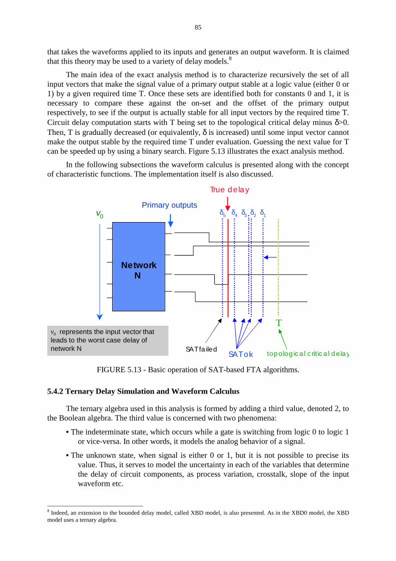
85
that takes the waveforms applied to its inputs and generates an output waveform. It is claimedthat this theory may be used to a variety of delay models.8
The main idea of the exact analysis method is to characterize recursively the set of allinput vectors that make the signal value of a primary output stable at a logic value (either 0 or1) by a given required time T. Once these sets are identified both for constants 0 and 1, it isnecessary to compare these against the on-set and the offset of the primary outputrespectively, to see if the output is actually stable for all input vectors by the required time T.Circuit delay computation starts with T being set to the topological critical delay minus δ>0.Then, T is gradually decreased (or equivalently, δ is increased) until some input vector cannotmake the output stable by the required time T under evaluation. Guessing the next value for Tcan be speeded up by using a binary search. Figure 5.13 illustrates the exact analysis method.
In the following subsections the waveform calculus is presented along with the conceptof characteristic functions. The implementation itself is also discussed.
v0 represents the input vector thatleads to the worst case delay ofnetwork N
Primary outputs
NetworkN
v0δ1δ2δ4δ5 δ3
True delay
T
topological critical delaySAT failed
SAT ok
FIGURE 5.13 - Basic operation of SAT-based FTA algorithms.
5.4.2 Ternary Delay Simulation and Waveform Calculus
The ternary algebra used in this analysis is formed by adding a third value, denoted 2, tothe Boolean algebra. The third value is concerned with two phenomena:
• The indeterminate state, which occurs while a gate is switching from logic 0 to logic 1or vice-versa. In other words, it models the analog behavior of a signal.
• The unknown state, when signal is either 0 or 1, but it is not possible to precise itsvalue. Thus, it serves to model the uncertainty in each of the variables that determinethe delay of circuit components, as process variation, crosstalk, slope of the inputwaveform etc.
8 Indeed, an extension to the bounded delay model, called XBD model, is also presented. As in the XBD0 model, the XBDmodel uses a ternary algebra.
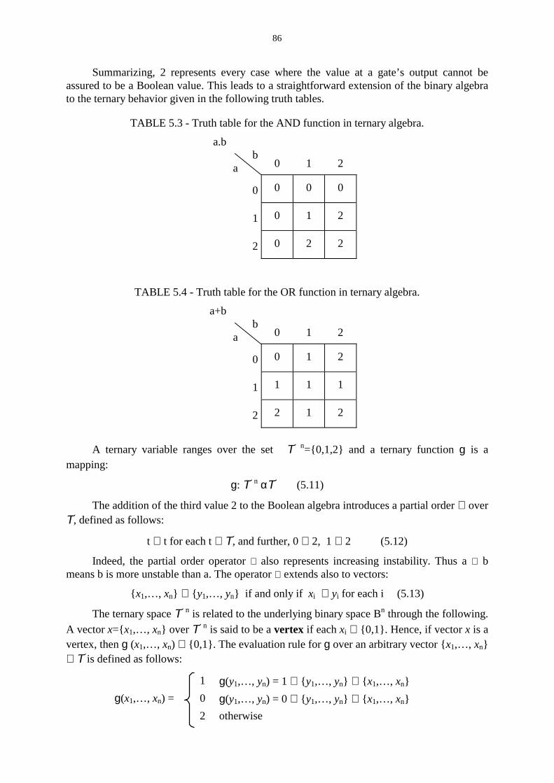
86
Summarizing, 2 represents every case where the value at a gate’s output cannot beassured to be a Boolean value. This leads to a straightforward extension of the binary algebrato the ternary behavior given in the following truth tables.
TABLE 5.3 - Truth table for the AND function in ternary algebra.
a.bb
a 0 1 2
0 0 0 0
1 0 1 2
2 0 2 2
TABLE 5.4 - Truth table for the OR function in ternary algebra.
a+bb
a 0 1 2
0 0 1 2
1 1 1 1
2 2 1 2
A ternary variable ranges over the set n=0,1,2 and a ternary function g is a
mapping:
g: n α (5.11)
The addition of the third value 2 to the Boolean algebra introduces a partial order ⊆ over, defined as follows:
t ⊆ t for each t ∈ , and further, 0 ⊆ 2, 1 ⊆ 2 (5.12)
Indeed, the partial order operator ⊆ also represents increasing instability. Thus a ⊆ bmeans b is more unstable than a. The operator ⊆ extends also to vectors:
x1,…, xn ⊆ y1,…, yn if and only if xi ⊆ yi for each i (5.13)
The ternary space n is related to the underlying binary space Bn through the following.
A vector x=x1,…, xn over n is said to be a vertex if each xi ∈ 0,1. Hence, if vector x is avertex, then g (x1,…, xn) ∈ 0,1. The evaluation rule for g over an arbitrary vector x1,…, xn∈ is defined as follows:
1 g(y1,…, yn) = 1 ∀ y1,…, yn ⊆ x1,…, xn
g(x1,…, xn) = 0 g(y1,…, yn) = 0 ∀ y1,…, yn ⊆ x1,…, xn
2 otherwise

87
The correspondence between vectors of the ternary space and cubes is evident. For thisreason, if g(x1,…, xn)=1, x1,…, xn is said to be an implicant of g. And a maximal suchimplicant is said a prime of g.
The evaluation rule gives rise to the following lemma:
Lemma 5.1:
Let g be an arbitrary function of x1,…, xm, where each xj ranges over the set 0,1,2.Let p1,…, pn be the primes of g and q1,…, qr be the primes of g’. Then, g(x1,…,xm)=2 if and only if there is no prime pi such that pi(x1,…, xm)=1 and no prime qi suchthat qi(x1,…, xm)=1.
In other words, the output of a gate is constant if the values applied to its inputs arecontained in a prime in the on-set or offset of the ternary function that represents it. And thisevaluation is independent of the gate structure.
A delay model augments this algebra by associating a time t with each value of a gate orwire; the value of a gate at time t, g(t) is a function of the values of the gate and its inputs oversome interval (t0,t1), where t1≤t.
Definition 5.1: waveform
Given a gate g, an associated waveform for g, Ωg, is a map:
Ωg : ℜ α 0,1,2 (5.14)
such that, for every t, every ε>0, if Ωg(t+ε)≠Ωg(t), Ωg(t+ε) and Ωg(t) both in 0,1, thenthere is some t<t1<t+ε such that Ωg(t1)=2.
The definition of a waveform models a logic signal varying over time. The restrictionthat any changes in signal forces a transition through 2 models the continuity of the physicalwaveform and that 0 and 1 are physically separate values. Figure 5.14 shows an example of aternary waveform.
1 2 0 1 2 02
Vhigh
Vlow
0
Vdd
0.800.90
1.101.25
1.803.30
1 2 0 1 2 02
Vhigh
Vlow
0
Vdd
0.800.90
1.101.25
1.803.30
FIGURE 5.14 - Example of ternary waveform.

88
Given a waveform Ω and a real interval I, the partial waveform of interval I, ΩI, is thewaveform Ω restricted to the domain I.
Definition 5.2: map for a gate
Map M for a gate G, with inputs f1,…, fr:
M : Ωf1(0,t) × Ωf2
(0,t) ×…× Ωfr(0,t) × ΩG
(0,t) α ΩG(t) (5.15)
is a delay model if for any subset S of inputs where Ωfs(0,t) is a constant function for
each s ∈ S, and cube c=∏s∈ S (fs=Ωfs(0,t)), G(c) is a constant, then ΩG(t)=G(c).
The definition treats transitions on a gate. The output waveform of a gate at t isdetermined by the input waveform as well as gate waveform occurring between 0 and sometime t’ preceding t. By convention, 0 is chosen as the base time; choosing a fixed base timefor all model mappings enforces the intuition that the value given by the delay model shouldbe independent of any time shift.
A Boolean algebra consists of a set of variables, each of which can assume a valuewithin 0,1; a combinational network, evaluated statically, is the realization of a functionover its input variables. A delay model, a network of gates and wires, a set of input variables,and a set of possible waveforms for each input variable yield a waveform algebra. Anassignment of one waveform to each input corresponds to an input waveform vector. The setof all waveform vectors forms a wave space, which (for n inputs) is denoted Wn. A waveformvector is the equivalent, in wave space, to an input vertex in Boolean space. Further, a pair(gate, delay model) is the equivalent, in wave space, to the gate in Boolean space. A pair(gate, delay model) takes an input wave and produces an output wave. This is illustrated infigure 5.15.
outputGb
a
2 10
020
2 21 0
Delay model for G
b
a
output
outputGb
aoutputGG
b
a
2 10 2 10
020 020
2 21 02 21 0
Delay model for G
b
a
output
FIGURE 5.15 - Delay model for a gate in the wave space.
The concept of characteristic functions also holds for the wave space.

89
Definition 5.3: characteristic function
A characteristic function over a wave space is a mapping:
χ : Wn α 0,1 (5.16)
conventionally, χ is associated with some set S ⊆ Wn: χ(w)=1 if and only if w ∈ S.
The exact analysis method uses extensively characteristic functions, particularly those ofthe form:
χ Ωg = w|w is a waveform producing waveform Ωg on signal g (5.17)
In current case, characteristic functions represent sets of waveform vectors. A waveformis an uncountable sequence of symbols from the set 0,1,2, representing the values of thewave at each real point in time t. However inputs are not toggled infinitely often. Thus, as aresult, there are relatively few waveform vectors of interest and these are easily encoded. Forexample, in most timing analysis problems, the inputs switch only once, at t=0. In this case,the waveform space Wn may be represented as the space Bn × Bn, where (v1,v2) represents thebinary input vectors applied at t=−∞ and t=0, respectively. Under these circumstances, thewave characteristic function is:
χ : Bn × Bn α 0,1 (5.18)
and is conveniently represented in the standard ways.
Specific delay computation models typically avoid an enumeration by giving rules forcomputing the output waveform given the input waveforms. In [MCG93] the various existingdelay computation models are discussed in the context of the ternary algebra. Here, thediscussion will be restricted to the bounded and unbounded delay models, renamed ExtendedBounded Delay model (XBD) and Extended Bounded Delay-0 model (XBD0), respectively
Under the XBD model, the delay associated to input i of gate g is within the range[di
min,dimax] and represents a transition region of uncertain width. As a result, pure translation
in time of the input waveform to the output is not allowed. The computation of Ωg(t) is givenas a two-step process:
Ω (t−di
max, t−dimin )
fi
Ω (t−di
max, t−dimin )
fi is a constantFi(t)=
2 otherwise
Ωg(t) = g(Fi(t), …, Fn(t) ) (5.19)
The values Fi(t) form “effective values” of the input waves, as presented to the output,at time t. If
Ω
(t−dimax, t−di
min )fi is a constant, then input fi has not changed over the interval
(t−dimax,t−di
min); since any change in the state of fi can only propagate to the output g at t ifthat change in state occurred between (t−di
max,t−dimin), it follows that the present state of input
fi is simply the constant state of the interval (t−dimax,t−di
min). If, on the other hand, fi changedstate between (t−di
max,t−dimin), then the presented value of the input might be any state of fi
between the intervals, or a transient; the only reasonable value to choose in suchcircumstances is 2. The value of Ωg(t) is then easily obtained as the static ternary evaluation ofg on the Fi(t).

90
The XBD0 model is equivalent to the XBD model, except that dimin=0 for any input i of
a gate g. The XBD0 model is the model underlying both viability [MCG89] and floating[CHEN93][DEV93] delay calculations.
5.4.3 Computing the Floating Delay under the XBD0 Model
Based on the waveform space concept and the associated definitions, the combinationaltiming verification problem can be defined.
Definition 5.4: combinational timing verification problem
Given a circuit C, a delay model M and a family of possible waveforms on thecombinational inputs of C such that each such waveform is a constant binary value on theintervals (−∞,0) and (t,∞) (i.e., each input changes state only in the interval (0,t)), thecombinational timing verification problem is to find the least positive d such that, for anypossible combination of input waveforms, Ωg
(d,∞) is a binary constant for each circuit outputg.
Under the XBD0 model, an input waveform for input a is one of two forms:
x(−∞,∞ )or
Ωa=
x(−∞,0)2[0,ta] x (ta,∞ )
where x ∈ 0,1 and ta is a positive constant associated with input a. This leads to thefollowing result concerning properties of circuit waveforms.
Lemma 5.2:
Let g be any gate in a logic circuit. Under the XBD0 model, under any waveform vector,Ωg(t) ∈ 1,0 for t>0 implies Ωg(t1) =Ωg(t) for all t1≥t.
The proof of lemma 5.2 is by induction. By definition, the result holds for the primaryinputs. Suppose it is true for all gates of level<N and consider a gate g at level N, and anarbitrary waveform w. Let Ωg be induced by w with Ωg(t)=1. We have g(f1, …, fn), and by theXBD0 evaluation model, 1 = Ωg(t) = g(F1(t), …, Fn(t)), where
Ω
(t−dimax, t)
fi
Ω
(t−dimax, t)
fi is a constantFi(t)=
2 otherwise
Since g(F1(t), …, Fn(t))=1, by lemma 5.1 there is some prime p of g, such that p(F1(t),…, Fn(t))=1. Consider an arbitrary t1>t. Since each input to g is of level<N, if Ωfi(t) ∈ 0,1,then by induction Ωfi(t1) ∈ 0,1, and hence Fi(t) ∈ 0,1 ⇒ Fi(t1) = Fi(t); hence, since p is apositive unate function of its literals, p(F1(t1), …, Fn(t1))=1, and by lemma 5.1 Ωg(t1)=1.
This lemma permits a characterization of the waves given by the XBD0 model.

91
Theorem 5.1:
Let g be any gate in a logic circuit. Under the XBD0 model and any allowed inputwaveform vector:
x(−∞,∞ )or
Ωg= x(−∞,0)2[0,tg] x (tg,∞ ) or
x(−∞,0)2[0,tg] x(tg,∞ )
for some x ∈ 0,1.
This theorem is an immediate consequence of the preceding lemma.
By this theorem, any waveform of a gate g is fully characterized. The next step is to usethe derived theory to resolve the timing analysis problem. Equation 5.17 states the following:
χ Ωg = w|w is a waveform producing waveform Ωg on signal g
Now, consider the set χΩ (t,∞ )
g ∈ 0,1.
This is the set of all input waveforms such that g is a binary constant on the interval(t,∞). Under the XBD0 model, the delay of a circuit with primary outputs o1,…,on, under inputwaveform vector w, is:
dw = max
imin t⊥ w∈ χ
Ω ( t,∞)oi ∈ 0,1
(5.20)
Hence the delay over all waveform vectors may be written:
dw = max
imin t⊥ χ
Ω (t,∞ )oi ∈ 0,1 = 1
(5.21)
It is important to note that d is the exact delay of the circuit. It is the exact minimumtime after which all outputs have stabilized. Thus, for any d1<d there is an input waveformvector and some output oi such that Ω
oi (di ) = 2. Now:
χΩ (t,∞ )
oi ∈ 0,1= χ
Ω (t,∞)oi =0
+ χΩ (t,∞)
oi =1(5.22)
From lemma 5.2.
χΩ (t,∞ )
g =0 = χ Ωg (t)=0 (5.23)
χΩ (t,∞ )
g =1 = χ Ωg (t)=1 (5.24)
Thus, it is necessary to calculate χΩg (t)=0 and χ
Ωg (t)=1 to complete the formulation forthe exact delay computation.

92
Lemma 5.3:
Let g be a gate with inputs f1,…, fr. Let p1,…, pn be all the primes of g, and q1,…, qn allthe primes of g’. Then:
χ Ωg (t)=1 = (pi (F1,...,Fr ) = 1)
i=1
n
∑ χ Ω fk (t−dkmax)= v
v⊆ Fk
∑k =1
r
∏ (5.25)
χ Ωg (t)=0 = (qj (F1,...,Fr ) =1)
j=1
m
∑ χ Ω fk (t−dkmax)=v
v⊆ Fk
∑k=1
r
∏ (5.26)
For the proof of this lemma consider the following. If w∈ χΩg (t)=1 , then Ωg(t)=1 when w
is applied as the input waveform vector. Hence there is some prime pi such thatpi(F1,…,Fr)=1, and, further, Fk ⊇ Ω
f k (t − dkmax) i.e.,
w ∈ χ Ω fk (t−dk
max)= v
v⊆ Fk
∑ (5.27)
for all k. Conversely, let w ∈ χ Ω fk (t−dk
max)= v
v⊆ Fk
∑ for all k, and, further, let pi(F1,…,Fr)=1. Then
Ωg(t)=1 by the evaluation rule, and hence w∈ χΩg (t)=1 .
The expression for both χΩg (t)=0 and χ
Ωg (t)=1 may be rewritten so that they depend onlyon the sensitization functions of the fanin of g.
Lemma 5.4:
Let g be a gate with inputs f1,…, fr. Let p1,…, pn be all the primes of g, and q1,…, qn allthe primes of g’. Let Fk(p) denote the value of input fk in a prime p. Then:
χ Ωg (t)=1 = Fk (pi )= 1( )⇒ χ Ω fk (t−dk
max)=1 Fk ( pi ) = 0( )⇒ χ Ω fk (t−dkmax)=0
k =1
r
∏i=1
n
∑ (5.28)
χ Ωg (t)=0 = Fk (qj ) =1( )⇒ χ Ω fk (t−dk
max)=1 Fk (qj ) = 0( )⇒ χ Ω fk (t−dkmax)=0
k =1
r
∏j=1
m
∑ (5.29)
These results follow from equations 5.25 and 5.26 because if Fk(p)=2, then
χ Ω fk (t− d)k
max=v
v⊆ Fk ( p)∑ =1
And this follows since for any gate fk,
χΩ fk (t−dk
max)= 0 + χ Ω fk (t− dkmax)=1 + χ Ω fk (t− dk
max)=2 =1
The previous equations suggest a recursive scheme for the computation of exact pathdelay under the XBD0 model. This can be accomplished by using the path recursive function
technique described in [MCG91a]. The sensitization functions χΩg (t)=0 and χ
Ωg (t)=1 at a gate gare computed using only the sensitization functions of its immediate fanin.
The overall process has two steps. In the first step the times for which sensitizationfunctions are required at each gate are determined by a reverse topological traversal: given alist of times at a gate g, the times required at each fanin fk are determined by subtracting the

93
delay from fk to g from each time in the list. In the second step, distinct path delays (fromprimary inputs) are determined at each gate; this is done by a forward propagation of pathlengths using a topological traversal. At the end of this step, for each gate g, there is a list oftimes required in computing the sensitization functions at g and a list of actual path lengths up
to g from any primary input. Suppose the sensitization function χΩg (tr )=1 is to be computed.
Let ta be the greatest path length to g such that ta ≤ tr. Since no event occurs between ta and tr,
χΩg (tr )=1 = χ Ωg (ta )=1 . This matching between required times and path lengths is performed at
each gate for each required time.
Finally, the characteristic functions of the sensitization functions Ωg(t)=1 and Ωg(t)=0are built up in topological order. A node representing a characteristic function is created foreach path length, which is matched by some required time. The function of each such node islinear in the number of primes of the gate (or its complement), and the number of fanin of thegate. The existence of a sensitizable path is determined by calling a satisfiability program, asdescribed in [MCG91a].
The complexity of the method deserves some comments. As mentioned by the authorsthemselves in [MCG93], in very large circuits and/or circuits with distinct delays on nearly allthe connections, the number of characteristic functions become very large. Indeed, if t is the
least time for which χΩg (t) is to be computed at a gate g, the number of functions required at
g is bounded above by the distinct path lengths between t and the longest path lengthterminating at g. This potential explosion may be alleviated by using some pruning rules.

94

95
6 Functional Timing Analysis of Circuits ContainingComplex Gates
Functional timing analysis has been massively investigated from the beginning ofcurrent decade. First FTA techniques performed single path sensitization by using a modifiedD algorithm and a variety of sensitization criteria. Indeed, in most of proposed criteria thesensitization conditions were kindly simplified attempting to reduce the time taken for testingconditions, while providing conservative (but still safe) delay estimates.
Since path-by-path identification of false paths has proved to be impractical, concurrentpath sensitization has come into focus. With concurrent path sensitization, FTA techniquesshifted from a “path enumeration-based false path identification” approach to a “delayenumeration-based delay computation” approach. Besides discarding the costly enumerationphase, concurrent path sensitization techniques have also allowed the use of the exactfloating-mode sensitization criterion, which uniquely furnishes the exact circuit delay underthe floating mode of operation.
However, all theory underlying the methods used to test path sensitizability and also thesensitization conditions themselves were developed assuming combinational circuits to bemade of simple gates, i.e., inverters, AND/NAND and OR/NOR gates. Consequently, if acombinational circuit containing more complex gates is to be analyzed, the FTA tool must beable to recognize such gates and treat the circuit properly under the adopted delaycomputation model. This may be accomplished either by adding a pre-processing phase or byextending the circuit delay computation method/algorithm and the sensitization conditions ofthe chosen criterion.
The availability of efficient CMOS macrocell generators, as the ones presented in[CAD99] and [MOR97], and efficient library-free technology mapping tools [REI97] hasmade possible the extensive use of complex gates (mainly static CMOS ones) in the physicaldesign of large combinational blocks. Hence, the ability of handling circuits containingcomplex gates became highly desirable for current FTA tools.
This chapter investigates FTA of circuits containing complex gates, which is intended tobe the main contribution of this thesis. Section 6.1 discusses some basic issues associated tothe technology mapping and layout generation making use of static CMOS complex gates(SCCGs). Section 6.2 discusses possible solutions for performing FTA of circuits containingcomplex gates. Section 6.3 presents an extended ATPG-based algorithm able to perform FTAof circuits containing complex gates.
6.1 Technology Mapping and Layout Generation for Circuits ContainingComplex Gates
In traditional VLSI physical design methods random logic blocks are generated usingpre-characterized (standard) cells from a library. The reasons for adopting this library-basedapproach were the ease of developing tools to automate layout generation and the goodelectrical performance predictability of the resulting design. However, the amazing evolutionof CMOS technology has shortened the life cycle of libraries: re-design and re-

96
characterization is becoming more frequent, which in turn increases the cost associated totheir maintenance. Another drawback of the library-based approach is the limited number ofprimitives: the higher is the number of cell options, concerning both function availability anddriving capability, the higher is the flexibility offered to the technology mapping tool.Obviously, this last tradeoff establishes a conflict, since libraries with many elements aremore expensive to maintain. A third issue is concerned with electrical performancepredictability. In current submicronic technologies, the delay introduced by the routingdominates over the delays of the gates. Hence, the linear physical model (see section 2.4),which is commonly used in delay estimation of cell-based layouts, is no longer able to offerthe required accuracy for assuring the correct operation of the fabricated design.
An alternative to the cell-based layout generation is the macrocell generation approach.A macrocell generator does not use cells from a library. Instead, it generates each element(transistors and connections) according to a layout pattern that is intrinsically programmedwithin its algorithms. The pioneer works on automatic cell generation were those of Lopezand Law [LOP80] and Uehara and Cleemput [UEH81]. The formers’ introduced a layout styleknown as gate matrix, while the latters’ presented the so-called linear matrix layout style.Both works were originally developed having in mind the automatic generation of celllibraries. Current macrocell generators are mainly based on the linear matrix style and are ableto generate combinational modules with up to some tenths of thousands of transistors[MOR94][MOR97][CAD99][EIJ94][GUR97].
A very important feature of macrocell generators is that they are potentially able togenerate any type of static CMOS gate. This introduces a new paradigm in the technologymapping problem, since the major part of existing technology mapping tools use the Booleanmatching technique, which is not an efficient solution for libraries with a large number ofelements [REI98]. This new problem is being referred to as the “library-free” or “virtuallibrary” technology mapping problem [REI95], due to the absence of a physical library ofcells. Recently proposed solutions for performing technology mapping over a virtual libraryrely on associating the arcs of the BDD that represents a given logic function to the transistorsof static CMOS gates [REI98][RIE96].
The shift from the traditional cell-based to the library-free layout generation strategy isunavoidable, not only because cell libraries became too expensive, but also because physicalmodels used to estimate performance (up till now) do not work for current CMOStechnologies.
On the other hand, the increase of flexibility provided by the library-free strategy mayonly be explored if appropriate tools are available. For instance, it is reported in [REI98] areduction in the total number of transistors when technology mapping considers not onlysimple CMOS gates (inverters, NAND and NOR gates), but also more complex static CMOSgates, generally referred to as SCCGs [REI95] (and formerly as supergates). This resultindicates a possible increase in the performance of designed circuits that must be carefullyinvestigated by the use of appropriate CAD tools.
Figure 6.1 shows a physical design flow using the FUCAS (FUll Custom AutomaticSynthesis) layout generation strategy [REI99]. Among the basic features of FUCAS, it isproposed the extensive use of SCCGs as a means of improving both logic density andelectrical performance. Within FUCAS strategy, the current macrocell generator to be used isTROPIC, which has been developed as part of a doctoral thesis [MOR94]. Concerningtechnology mapping for SCCGs, there is a specific tool under development calledTRABUCO, which is the evolution of a technology mapping prototype called TABA [REI98].

97
testing
test vector generation
test vectors
layout extraction
cell layout patterns
logic-level simulation ok?
y
n
timing verification (FTA) ok?
y
n
placement
cell generation
routing
mapped logic-level description
circuit layout
tech. mapping TABA/TRABUCO
initial logic-level description
optimized logic-level description
logic synthesis and optimization
(e.g. SIS)
prototyping
circuitprototype
timing verification (FTA) ok?
y
n
testingtesting
test vector generationtest vector generation
test vectorstest vectors
layout extractionlayout extraction
cell layout patterns
cell layout patterns
logic-level simulationlogic-level simulation ok?ok?
y
n
timing verification (FTA)
timing verification (FTA) ok?ok?
y
n
placement
cell generation
routing
mapped logic-level description
circuit layout
tech. mapping TABA/TRABUCO
initial logic-level description
optimized logic-level description
logic synthesis and optimization
(e.g. SIS)
prototyping
circuitprototype
placementplacement
cell generationcell generation
routingrouting
mapped logic-level descriptionmapped logic-
level description
circuit layoutcircuit layout
tech. mapping TABA/TRABUCO
tech. mapping TABA/TRABUCO
initial logic-level description
initial logic-level description
optimized logic-level descriptionoptimized logic-level description
logic synthesis and optimization
(e.g. SIS)
logic synthesis and optimization
(e.g. SIS)
prototypingprototyping
circuitprototype
timing verification (FTA)
timing verification (FTA) ok?ok?
y
n
FIGURE 6.1 - Physical design flow using the FUCAS layout generation strategy.
The design flow with the FUCAS strategy obviously requires a timing verification toolable to validate the timing requirements of designs. Hopefully, such tool must be able toprovide fast, safe and accurate delay estimates of large combinational blocks containingSCCGs that will be used to guide the physical design as a whole. Doubtlessly, the timinganalysis technique is the natural choice for performing timing verification because it is input-stimuli independent. Furthermore, it presents a lower computation cost when comparing tocircuit simulation, thus being much faster. Within timing analysis techniques, functionaltiming analysis is the one able to provide the most accurate estimates. Hence, the physicaldesign with FUCAS represents a real need for a FTA tool able to handle complex gates.

98
6.1.1 Simple Gates, General Complex Gates and Static CMOS Complex Gates
The expressions “simple gates” and “complex gates” are intensively used in the fields oflogic synthesis, technology mapping, test generation and timing analysis. As long as suchexpressions may be employed with slightly different meanings in each of the mentionedfields, it seems to be advisable beginning by redefining them within the context of the currentwork.
In the context of this thesis, a simple gate corresponds to a (possible) physicalimplementation of the basic operators of the Boolean algebra, complemented or not. Thus, thewhole set of simple gates may be enumerated as follows: n-input AND, OR, NAND, NORgates and the inverter (sometimes called NOT gate), with n = 2, 3, 4,…. Particularly, the setof simple CMOS gates is a subset of the simple gates set, since the basic Boolean operatorsthat may be directly implemented with the CMOS technology are: n-input NAND, NOR gatesand inverters.
A general complex gate, or simply complex gate, corresponds to a physicalimplementation of any single output Boolean function of higher complexity than the basicBoolean operators. Strictly speaking, a static CMOS complex gate, or SCCG for shortly,corresponds to a complex gate implemented using the CMOS technology. Consequently, anySCCG implements an inverting Boolean function.
Although this work is intended to investigate FTA algorithms that are able to operate ongeneral complex gate networks, let us first turn our attention to the SCCG case, as a first stepfor extending FTA theory for complex gates and at the same time, taking advantage on thereal-case design opportunity provided by the FUCAS design strategy.
A static CMOS gate may also be classified as a “full restoring” network of CMOStransistors because it is composed of two distinct networks of transistors: a PMOS transistornetwork connected between the power supply (Vdd) and the gate output and a NMOStransistor network connected between the ground (Gnd) and the gate output. The networkshave equal number of transistors and are commonly referred to as NMOS-network andPMOS-network. For the sake of simplicity, we are going to assume that a SCCG is a staticCMOS gate in which both networks are made up from serial/parallel only associations andalso that the NMOS-network is the dual of the PMOS-network, in terms of transistorassociation. Figure 6.2 shows an example of SCCG. Note that, for an n-input static CMOSgate, there are n pairs of NMOS-PMOS transistors connected together through the gateterminal to form each of the n inputs to the gate.
It is interesting to notice that in a simple CMOS gate the NMOS and PMOS networksare either parallel only or series-only. On the other hand, SCCGs present series/paralleltransistor NMOS and PMOS transistor networks with at least 3 inputs.
Static CMOS gates (including SCCGs) may be classified according to the number ofserial/parallel transistors encountered in their NMOS/PMOS networks. The set of staticCMOS gates formed by no more than n (p) serial NMOS (PMOS) transistors is referred to asvirtual “library” [REI98] and may be designated by SCG(n,p). We may also use the notationSCCG(2,2) to designate the subset of SCG(2,2) formed by SCCGs only. Figure 6.3 (borrowedfrom [REI98]) shows the elements of the set SCG(2,2), while table 6.1 (also borrowed from[REI98]) shows the number of elements for various virtual libraries.

99
(b)
S
GND
VDD
A
A
B
B
C
C
D
D
E
E
A
CS
B
D
E
(a)
(b)
S
GND
VDD
A
A
B
B
C
C
D
D
E
E
(b)
S
GND
VDD
A
A
B
B
C
C
D
D
E
E
S
GND
VDD
A
A
B
B
C
C
D
D
E
E
A
CS
B
D
E
(a)
A
CS
B
D
E
A
CCS
BB
DD
EE
(a)
FIGURE 6.2 - Example of SCCG.
FIGURE 6.3 - Elements of the virtual library SCG(2,2) [REI98].
TABLE 6.1 - Number of elements for various virtual libraries [DET87].
number of serial PMOS transistors
1 2 3 4 5
1 1 2 3 4 5
2 2 7 18 42 90
3 3 18 87 396 1677
4 4 42 396 3503 28435
number ofserial
NMOStransistors
5 5 90 1677 28435 425803

100
6.2 The Applicability of Existing Functional Timing Analysis Techniquesfor Circuits Containing Complex Gates
Although many FTA algorithms were developed in the past decade, most of them arenot able to work directly on circuits containing complex gates. In the case of ATPG-basedalgorithms, such limitation is due to the fact that all sensitization theory has been developedfor simple gates only. Of course, the extension of sensitization criteria to complex gatesresults in more complicated rules, making traditional single path sensitizability testing evenmore complicated. At a first glance, SAT-based algorithms seem to be more promising sincecharacteristic equations are potentially able to represent any Boolean function. However, inorder to reduce the complexity in solving SAT instances, some SAT-based algorithms assumesimple gates-only combinational circuits.
The simplest solution for treating circuits with complex gates relies on replacing eachcomplex gate by an equivalent sub-circuit composed of simple gates. This technique is knownas macro-expansion and offers the advantage of allowing the use of gate-level FTA toolsoriginally developed for simple gates [MCG91][HSU98]. Macro-expansion presents twosevere drawbacks, however [HSU98]. Firstly, it is very difficult to accurately model the delayof macro-expanded complex gates. Consequently, the resulted circuit delay estimates may notbe sufficiently accurate. The use of sophisticated delay models for macro-expanded gates canreduce this loss in accuracy, but may overly increase the complexity of the macro-expansionstep, also increasing the overall execution time. Secondly, macro-expansion proceduresincrease the number of nodes in the circuit graph. In an ATPG-based algorithm, extra nodesrepresent potential extra circuit lines to be justified. In the case of SAT-based algorithms, eachextra node originates an extra characteristic function. In any case, the overhead in executiontime will depend on the complexity of equivalent sub-circuits used to model complex gates.
The second possible solution relies on modifying the sensitization tests in order tohandle complex gates. Such modifications include not only the sensitization criterion but alsothe sensitization testing algorithm itself. Since path sensitizability testing may beaccomplished by different algorithms, this solution represents indeed a group of possiblesolutions.
In [HSU98], for instance, a FTA algorithm able to operate directly on circuits containingcomplex gates is presented. In order to avoid macro-expansion, the exact floating-modesensitization conditions are extended to consider complex gates. The extended sensitizationconditions are then used within a single path sensitization procedure derived from theclassical D-algorithm. The practical results presented in [HSU98] allow for a comparisonbetween some macro-expansion procedures, featuring different delay models for complexgates, and the direct application of the extended sensitization criterion. However, all resultswere obtained through the use of a single path sensitization algorithm. Although theadvantage of directly treating sensitization of complex gates becomes clear, single pathsensitization procedures suffer from the path explosion problem and thus do not represent thestate-of-the-art in FTA.
As presented in section 5.3, the timed-test generation procedure of Devadas et al.[DEV93a] is an ATPG-based multiple path sensitization algorithm derived from the PODEM[GOE81] test generation algorithm. In the timed-test generation procedure the delaycomputation problem is transformed into a set of single stuck-at fault test generations inwhich the algorithm tries to justify “timed” stuck-at faults at the primary outputs of the circuit.This is accomplished by using an appropriate subset of PODEM functions along with a set of

101
three-valued timed calculus rules that allows the application of “timed” logic values throughthe circuit lines. The three-valued timed calculus assumes the exact floating-modesensitization criterion. Although the possibility of extending this procedure to circuitscontaining complex gates is mentioned in [DEV93a], this issue is not further detailed.
SAT-based algorithms, and especially the one presented in section 5.4 [MCG93],implicitly consider path sensitizability by applying the concept of sensitization characteristicfunctions. The characteristic functions are computed recursively for each circuit node,assuming a given required time T at the circuit outputs. The elegance of this approach relieson the fact that characteristic functions are potentially able to represent any type of Booleanfunctionality, including the general complex gate case. However, SAT solver algorithms areheavily CPU intensive and the only way to make the approach feasible for timing analysis isto control the size of the SAT problem, or equivalently, the size of the characteristic functionsnetwork. Kukimoto et al. [KUK97] observes that using the two basic pruning rules presentedin [MCG93] is not sufficient to assure that the method can be used in the analysis of morecomplex designs, and proposes two approximation schemes. One of them is based ondesigner’s knowledge of circuits (the control/data dichotomy proposed in [YAL95]). Theother one concerns a simplification on calculating arrival times at circuit gates. Unfortunately,both approximations may result in a significant loss of accuracy, which may partially cancelthe gain obtained in execution time.
Another problem with the SAT-based approach relies on the fact that the use of moreaccurate delay models increases the number of SAT instances that must be solved due towrong decisions taken during the solving steps. In order to alleviate this problem, Silvaproposed in [SIL99] a mixed approach that maintains circuit structure information while usinga SAT solver. By doing so, it is possible to apply acceleration techniques commonly used intest generation, as non-chronological backtracking and recursive learning.
Due to the mentioned difficulties presented by SAT-based implementations andconsidering that many acceleration techniques exist for ATPG algorithms, the use of thetimed-test generation procedure to work directly on combinational blocks containing complexgates seems to be the most promising possibility, in terms of both CPU execution time anddelay estimate accuracy. Hence, the rest of this chapter is devoted to further investigate thisoption.
6.3 ATPG-Based FTA of Circuits Containing Complex Gates
Although the timed-test generation procedure has already been addressed in subsection5.3.3, it will be necessary to go deeper into the implementation details in order to detect whichmodifications are needed to allow it operating directly on circuits containing complex gates.
The timed-test generation procedure serves as the core of the ATPG-based concurrentpath sensitization FTA algorithm called TrueD-F [DEV93a]. Therefore, before proceed theanalysis of the timed-test generation procedure itself it is convenient to examine how TrueD-Fcomputes the floating delay of a combinational block.
Consider a single-output combinational block. TrueD-F determines the maximum delayat the block’s output by answering the question “is this delay greater than or equal δ?” δ isinitially set to T-ε0, where T is the circuit topological delay and ε0 is a small quantity greaterthan 0. To answer the question, input cube simulation is accomplished by using a modifiedversion of the PODEM algorithm [GOE81], the so-called “timed-test generation procedure”

102
[DEV93a]. While the answer to the question is “no”, the timed-test generation procedure issuccessively called for δi = T-εi, with i=0,1,2,...., εi+1 > εi. A “yes” answer means that theoutput’s maximum delay is between the current value of δ (say T-εk) and the previous one (T-εk-1). Hence, T-εk-1 represents a safe upper bound on the maximum delay of current output. Incase a more accurate delay value is needed a binary search may be performed on the interval[T-εk , T-εk-1].
Since the block’s output may stabilize either with logic value 0 or with logic value 1, thetimed-test procedure must be performed twice for each delay value δi (except in case a “yes”answer occurs for the first logic value tested). Figure 6.4 depicts the timed-test generationprocedure.
In the case of a multi-output combinational block, the timed-test generation proceduremust be called for each output for both 0 and 1 logic values and for each δi. A firstapproximation to the lower bound on the circuit delay (i.e., T-εk) is determined by the first“yes” answer arriving.
true delay(unknown)
delay
T-ε1T-ε2T-ε3T-ε4 T
topological delay
“no”“yes” true delay(unknown)
delay
T-ε1T-ε1T-ε2T-ε2T-ε3T-ε3T-ε4T-ε4 T
topological delay
T
topological delay
“no”“no”“yes”“yes”
FIGURE 6.4 - Timed-test generation procedure applied to a single-output circuit.
In order to determine whether the delay of a circuit’s output is greater than or equal toδi for a logic value lvalue, the timed-test procedure tries to justify lvalue at the consideredoutput with delay greater than or equal δi. This is done by using cube simulation, in aPODEM-like fashion. Since PODEM allows for a systematic and exhaustive exploration ofthe input space, once it fails in finding an input cube that justifies lvalue at a circuit’s outputunder the considered delay δi, then the answer to the question is “no” for that output (and forlogic value lvalue). In other words, the problem of determining the maximum delay istransformed into a test generation problem for a single stuck-at fault at the circuit’s output.
The topmost call of the procedure timed_test is described by the pseudo-code in figure6.5. As in the purely logical PODEM, there is a justification list jlist holding circuit linesthat must be justified. The procedure begins by inserting a given primary output line po intojlist with logic value lvalue (either 0 or 1) and assuming delay as circuit delay lowerbound to be tested (δi). Then, procedure SEARCH_1 is called.
timed_test(po,delay,lvalue) v.value = lvalue; v.lower = delay; v.upper = INFINITY;
modify_jlist (po,v,jlist); backward schedule po;
status = SEARCH_1(jlist); return(status);
FIGURE 6.5 - Pseudo-code for the topmost call of the timed-test generation procedure.

103
The search procedures are described by the pseudo-codes of figures 6.6 and 6.7. Theyare similar to the search procedures of PODEM. The procedure SEARCH_1 calls a BACKTRACEprocedure to find a primary input which logical value is currently unknown, beginning fromthe primary output po. The primary input is (initially) set to logic value 1 and the IMPLYprocedure is called. This procedure performs a timed-test cube simulation that considers exactfloating-mode sensitization conditions (in PODEM, it corresponds to three-valued cubesimulation without any delay information). The implication procedure may produce a logicalor a temporal conflict. If no conflict occurs, SEARCH_1 is called recursively. The procedureterminates successfully in SEARCH_1 if the justification list is empty. In case a conflict occursin SEARCH_1 the algorithm backtracks to the most recent primary input assignment. Theprimary input is set to logic value 0, and SEARCH_2 procedure shown in figure 6.7 is called.
Failure results if either the BACKTRACE procedure is unable to find a primary input to setor if the space has been completely explored without success in SEARCH_2. A conflict occurswhen it is not possible to set a given circuit line to the required logic value at the requiredtime. In the case of conflict or failure, the network must be restored to the state it wasimmediately prior to the primary input setting that caused the conflict or the failure.
SEARCH_1(jlist)if(length of jlist is zero) return SUCCEED;
if(BACKTRACE(gate,value,delay,&pi,&pi_value)==FALSE)return(FAILED);
if(IMPLY(pi,pi_value,jlist)!=IMPLY_CONFLICT)search_status = SEARCH_1(jlist);if(search_status == FAILED)restore the state of the network;search_status = SEARCH_2(jlist,pi,1-pi_value);
else
restore the state of the network;search_status = SEARCH_2(jlist,pi,1-pi_value);
return(search_status);
FIGURE 6.6 - Pseudo-code for the first search procedure.
The timed-test generation procedure assumes that each circuit gate (and additionally,each circuit edge) has a “timed-value” variable, composed of three fields: a lower and anupper bound on the delay of the gate (actually, stable times) and a logic value. A pre-processing step initializes all logic values to the unsigned value, i.e. 2, and lower and upperbounds to the minimal and maximal topological delays from any primary input. In the testgeneration phase, while primary inputs are set to known logic values, the delay bounds aretightened during the forward simulation due to the sensitization or blocking of paths. Thelower and upper bounds are also modified by backward implication, by the time new valuesare inferred at particular gates, given logic and delay values requirements at the primaryoutputs.
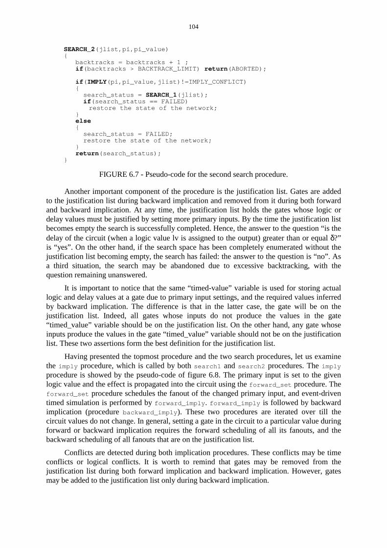
104
SEARCH_2(jlist,pi,pi_value) backtracks = backtracks + 1 ; if(backtracks > BACKTRACK_LIMIT) return(ABORTED);
if(IMPLY(pi,pi_value,jlist)!=IMPLY_CONFLICT) search_status = SEARCH_1(jlist); if(search_status == FAILED) restore the state of the network;
else
search_status = FAILED; restore the state of the network; return(search_status);
FIGURE 6.7 - Pseudo-code for the second search procedure.
Another important component of the procedure is the justification list. Gates are addedto the justification list during backward implication and removed from it during both forwardand backward implication. At any time, the justification list holds the gates whose logic ordelay values must be justified by setting more primary inputs. By the time the justification listbecomes empty the search is successfully completed. Hence, the answer to the question “is thedelay of the circuit (when a logic value lv is assigned to the output) greater than or equal δ?”is “yes”. On the other hand, if the search space has been completely enumerated without thejustification list becoming empty, the search has failed: the answer to the question is “no”. Asa third situation, the search may be abandoned due to excessive backtracking, with thequestion remaining unanswered.
It is important to notice that the same “timed-value” variable is used for storing actuallogic and delay values at a gate due to primary input settings, and the required values inferredby backward implication. The difference is that in the latter case, the gate will be on thejustification list. Indeed, all gates whose inputs do not produce the values in the gate“timed_value” variable should be on the justification list. On the other hand, any gate whoseinputs produce the values in the gate “timed_value” variable should not be on the justificationlist. These two assertions form the best definition for the justification list.
Having presented the topmost procedure and the two search procedures, let us examinethe imply procedure, which is called by both search1 and search2 procedures. The implyprocedure is showed by the pseudo-code of figure 6.8. The primary input is set to the givenlogic value and the effect is propagated into the circuit using the forward_set procedure. Theforward_set procedure schedules the fanout of the changed primary input, and event-driventimed simulation is performed by forward_imply. forward_imply is followed by backwardimplication (procedure backward_imply). These two procedures are iterated over till thecircuit values do not change. In general, setting a gate in the circuit to a particular value duringforward or backward implication requires the forward scheduling of all its fanouts, and thebackward scheduling of all fanouts that are on the justification list.
Conflicts are detected during both implication procedures. These conflicts may be timeconflicts or logical conflicts. It is worth to remind that gates may be removed from thejustification list during both forward implication and backward implication. However, gatesmay be added to the justification list only during backward implication.

105
imply(pi,pi_value,jlist) v = pi.timed_value; v.value = pi_value; status = forward_set(pi,v,jlist);
while(status==IMPLY_NORMAL) status=forward_imply(jlist);
if(status!=IMPLY_CONFLICT)status=backward_imply(jlist);
return status;
FIGURE 6.8 - Pseudo-code for the imply procedure.
The key for determining whether it is possible to justify a logic value at a circuit’soutput within the required time or not relies on using a three-valued timed calculus that takesinto account the conditions stated by the exact floating-mode sensitization criterion. Considera 2-input AND gate with delay d. Each input ii of the gate may present a logic value in 0,1,2with lower and upper bounds on its delay given by li and ui, respectively. The term “delay of asignal” will be used rather than “stable time” [CHE93] because even gates presenting thevalue 2 at the output have lower and upper delays. The timed calculus for cube simulation for2-input AND gates and 2-input OR gates are given in tables 6.2 and 6.3, respectively. In thesetables lv is the logic value at the gate’s output, while lo and uo represent the lower and theupper bounds on the delay at the gate’s output, respectively.
TABLE 6.2 - Three-valued timed calculus for a 2-input AND gate.
i2
i10 1 2
0lvlouo
0min(l1,l2)+d
min(u1,u2)+d
0l2+du2+d
0min(l1,l2)+d
u2+d
1lvlouo
0l1+du1+d
1max(l1,l2)+d
max(u1,u2)+d
2l1+d
max(u1,u2)+d
2lvlouo
0min(l1,l2)+d
u1+d
2l2+d
max(u1,u2)+d
2min(l1,l2)+d
max(u1,u2)+d
TABLE 6.3 - Three-valued timed calculus for a 2-input OR gate.
i2
i10 1 2
0lvlouo
0max(l1,l2)+d
max(u1,u2)+d
1l1+du1+d
2l1+d
max(u1,u2)+d
1lvlouo
1l2+du2+d
1min(l1,l2)+d
min(u1,u2)+d
1min(l1,l2)+d
u2+d
2lvlouo
2l2+d
max(u1,u2)+d
1min(l1,l2)+d
u1+d
2min(l1,l2)+d
max(u1,u2)+d

106
6.3.1 Extending the Timed-Calculus to Complex Gates
The rules presented in tables 6.2 and 6.3 are easily extended to n-input AND and ORgates. Furthermore, they may also be extended to NAND and NOR gates if gate functionpolarity is accounted for. Therefore, before considering their use for complex gates, it isconvenient to generalize the three-valued timed calculus to any type of n-input simple gates.In order to do that, let us first recall the concepts of controlling/non-controlling andcontrolled/non-controlled values, as they are defined within ATPG theory. Thecontrolling/controlled value of an AND (OR) gate g, c(g)/cd(g) is logic 0 (logic 1), while thenon-controlling/non-controlled value of an AND (OR) gate g, nc(g)/ncd(g), is logic 1 (0).Then, given an n-input AND/OR gate g, we may classify the cases listed in tables 6.2 and 6.3according to the following groups:
1. Cases in which at least one of the inputs of g presents a controlling value (c(g)). Theothers may present either non-controlling values (nc(g)) or the 2 value;
2. The case in which all inputs of g present non-controlling values (nc(g));3. Cases in which at least one of the inputs of g presents a 2 value, but none presents a
controlling value (c(g)). The others may present non-controlling values (nc(g)).Now, we may generalize the timed-calculus for simple gates, and at the same time
include NAND and NOR gates, by the rules listed in table 6.4.
TABLE 6.4 - Generalized three-valued timed calculus for n-input simple gates.
group rules lv
1louo
min li | i= c(g) or i=2 + dmin uj | j= c(g) + d
pol(g) ⊕ c(g)
2louo
max li + dmax uj + d
pol(g) ⊕ nc(g)
3louo
min li | i=2 + dmax uj + d
2
Now, in order to apply the rules of table 6.4 to AND gates, for instance, one has toassume c(g)=0, nc(g)=1 and pol(g)=0. In the case of a NOR gate, c(g)=1, nc(g)=0 andpol(g)=1. Each of the three groups of rules are further illustrated by figures 6.9, 6.10 and 6.11,respectively. Note that for the ease of explanation, we have assumed a single delay per gate.More sophisticated gate delay computation models may also be used, however. Subsection6.3.2 elaborates more on the gate delay computation model issue.
The extension of the generalized three-valued timed calculus to complex gates isstraightforward since we assume each gate function to be represented as a factored form,using a convenient data structure. For instance, consider the SCCG of figure 6.2, re-edited in
figure 6.12. The logic function implemented by this gate, S = A ⋅((B ⋅C) +(D ⋅E)) , is easilyretrieved from its transistor-level description and may be represented as a tree. By examiningthis “function tree” one notice that, given an assignment of input timed-values (logic valueswith lower and upper bounds on delays), the corresponding output timed-values may becomputed by successively applying the rules showed in table 6.4 to each subtree, beginningfrom the bottom most, since the following is assumed:

107
1. All subtrees, except the topmost one, have no delay and polarity equals zero
2. The gate delay is applied to the gate output lower and upper bounds, i.e., only to thetimed-values resulted from the evaluation of the topmost subtree.
3. gate polarity is treated when the topmost subtree is processed.
i1
i2
i3
og
i4
l1 u1c(g)
2l2 u2
l3 u3c(g)
u4l4nc(g)
min li | i= c(g) or i=2 + d
min uj | j= c(g) + d
pol(g) ⊕ c(g)
l2 + d u1 + d
d= gate delay
i1
i2
i3
og
i4
i1
i2
i3
og
i4
l1 u1c(g)
2l2 u2
l3 u3c(g)
u4l4nc(g)
l1 u1c(g)
l1 u1c(g)c(g)
2l2 u2
2l2 u2
l3 u3c(g)
l3 u3c(g)c(g)
u4l4nc(g)
u4l4nc(g)nc(g)
min li | i= c(g) or i=2 + d
min uj | j= c(g) + d
pol(g) ⊕ c(g)
l2 + d u1 + d
d= gate delay
FIGURE 6.9 - Three-valued timed calculus for group 1.
l1 + d u3 + d
max li + d max uj + d
pol(g) ⊕ nc(g)
l1 u1nc(g)
nc(g)l2 u2
l3 u3nc(g)
u4l4nc(g)
i1
i2
i3
og
i4
d= gate delay
l1 + d u3 + d
max li + d max uj + d
pol(g) ⊕ nc(g)
l1 u1nc(g)
nc(g)l2 u2
l3 u3nc(g)
u4l4nc(g)
l1 u1nc(g)
l1 u1nc(g)nc(g)
nc(g)l2 u2
nc(g)l2 u2
l3 u3nc(g)
l3 u3nc(g)nc(g)
u4l4nc(g)
u4l4nc(g)nc(g)
i1
i2
i3
og
i4
i1
i2
i3
og
i4
d= gate delay
FIGURE 6.10 - Three-valued timed calculus for group 2.
l2 + d u3 + d
min li | i=2 + d max uj + d
l1 u1nc(g)
2 l2 u2
l3 u32
u4l4nc(g)
i1
i2
i3
og
i4
2
d= gate delay
l2 + d u3 + d
min li | i=2 + d max uj + d
l1 u1nc(g)
2 l2 u2
l3 u32
u4l4nc(g)
l1 u1nc(g)
l1 u1nc(g)nc(g)
2 l2 u2
2 l2 u2
l3 u32
l3 u322
u4l4nc(g)
u4l4nc(g)nc(g)
i1
i2
i3
og
i4
i1
i2
i3
og
i4
2
d= gate delay
FIGURE 6.11 - Three-valued timed calculus for group 3.
The first and second assumptions allow us to split the timed evaluation of a SCCG intotwo independent steps. In the first step the output logic value and the lower and upper boundswith zero gate delay are computed. We may call such delay interval as “first-order delay

108
bounds”. In the second step actual lower and upper bounds are computed by adding the gatedelay to the first order delay bounds.
(b)
S
GND
VDD
A
A
B
B
C
C
D
D
E
E
A
CS
B
D
E
(a)
+
. .
A
D EB C
.
(c)
(b)
S
GND
VDD
A
A
B
B
C
C
D
D
E
E
(b)
S
GND
VDD
A
A
B
B
C
C
D
D
E
E
S
GND
VDD
A
A
B
B
C
C
D
D
E
E
A
CS
B
D
E
(a)
+
. .
A
D EB C
.
(c)
A
CS
B
D
E
(a)
A
CS
B
D
E
A
CCS
BB
DD
EE
(a)
+
. .
A
D EB C
.
(c)
+
. .
A
D EB C
.
+
. .
A
D EB C
.
(c)
FIGURE 6.12 - Example of SCCG: logic-level symbol (a), transistor schematics (b) andfunction tree (c).
In order to facilitate its comprehension and also its use, we may rewrite the three-valuedtimed calculus rules to be used in the first step of SCCG evaluation as shown in table 6.5.
TABLE 6.5 - Three-valued timed calculus for evaluating SCCGs.
lower subtrees topmost subtreegroup first-order delay bounds lv output lv
1louo
min li | i= c(g) or i=2 min uj | j= c(g)
c(g) pol(g) ⊕ c(g)
2louo
max li max uj
nc(g) pol(g) ⊕ nc(g)
3louo
min li | i=2 max uj
2 2
Figure 6.13 illustrates the three-valued timed-test evaluation procedure on the SCCG offigure 6.12. The intermediate dummy nodes shown in this figure are actually dispensable incase of a recursive implementation.
It is interesting to notice that in case of SCCGs, all subtrees belonging to the same levelcorresponds to either the same logic operation or to a leaf. In the (original) function tree a leafrepresents a gate input. Another property of SCCG function trees concerns the fact that anytwo subsequent levels present different logic operations, either AND or OR.
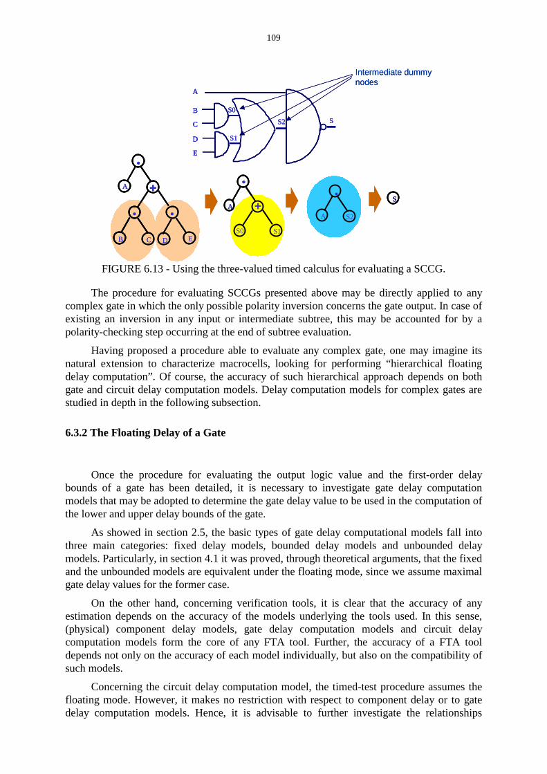
109
A
C
B
D
E
S
S0
S1
S2
A S2
.S
+A
S0 S1
.
Intermediate dummy nodes
+
. .
D EB C
.
A
A
C
B
D
E
S
S0
S1
S2
A
C
B
D
E
A
C
B
D
E
S
S0
S1
S2
A S2
.A S2
.SS
+A
S0 S1
.
+A
S0 S1
.
Intermediate dummy nodes
+
. .
D EB C
.
A +
. .
D EB C
.
A
FIGURE 6.13 - Using the three-valued timed calculus for evaluating a SCCG.
The procedure for evaluating SCCGs presented above may be directly applied to anycomplex gate in which the only possible polarity inversion concerns the gate output. In case ofexisting an inversion in any input or intermediate subtree, this may be accounted for by apolarity-checking step occurring at the end of subtree evaluation.
Having proposed a procedure able to evaluate any complex gate, one may imagine itsnatural extension to characterize macrocells, looking for performing “hierarchical floatingdelay computation”. Of course, the accuracy of such hierarchical approach depends on bothgate and circuit delay computation models. Delay computation models for complex gates arestudied in depth in the following subsection.
6.3.2 The Floating Delay of a Gate
Once the procedure for evaluating the output logic value and the first-order delaybounds of a gate has been detailed, it is necessary to investigate gate delay computationmodels that may be adopted to determine the gate delay value to be used in the computation ofthe lower and upper delay bounds of the gate.
As showed in section 2.5, the basic types of gate delay computational models fall intothree main categories: fixed delay models, bounded delay models and unbounded delaymodels. Particularly, in section 4.1 it was proved, through theoretical arguments, that the fixedand the unbounded models are equivalent under the floating mode, since we assume maximalgate delay values for the former case.
On the other hand, concerning verification tools, it is clear that the accuracy of anyestimation depends on the accuracy of the models underlying the tools used. In this sense,(physical) component delay models, gate delay computation models and circuit delaycomputation models form the core of any FTA tool. Further, the accuracy of a FTA tooldepends not only on the accuracy of each model individually, but also on the compatibility ofsuch models.
Concerning the circuit delay computation model, the timed-test procedure assumes thefloating mode. However, it makes no restriction with respect to component delay or to gatedelay computation models. Hence, it is advisable to further investigate the relationships

110
between these models, in order to identify the existing options, as well as their respectiveaccuracies.
As mentioned in the previous paragraph, the timed-test procedure computes the floatingdelay of a circuit. Thus, the study starts by assuming the floating mode circuit delaycomputation model. In addition, this study targets at investigating the circumstances underwhich the most accurate estimates are achieved and which is the computational effortinvolved.
In order to establish relationships between the circuit delay computation model and bothgate delay computation and physical models, consider the inverter of figure 6.14(a). Consideralso the application of the logic value 1 at the inverter’s input, which will result in the logicvalue 0 at its output. As long as the floating mode does not make assumptions on the previousstate of circuit nodes, under such delay model, the 1 at the inverter’s input may representeither a rising transition or a steady 1. Given this, it results that the 0 at the inverter’s outputmay be either a falling transition or a steady 0 (figure 6.14(b)). However, in order not tounderestimate the circuit delay, we have to consider the worst case, that is, a falling outputtransition.
Note that, although the floating mode does not make any assumption on the previousstate of a node, the whole history needed for analyzing the inverter of figure 6.14(a)corresponds to the two input situations shown in figure 6.14(b). Thus, in the inverter case, thefalling delay under the floating mode corresponds to the falling delay under the transitionmode. By equivalent arguments, it is possible to affirm that the rising floating delay of theinverter corresponds to its rising transition delay.
1 0 0 or ↓1 or ↑
a floating vector underlying pairs of vectors
(a) (b)
1 0 0 or ↓1 or ↑
a floating vector underlying pairs of vectors
(a) (b)
FIGURE 6.14 - The relationship between floating mode (a) and transition mode (b).
Consider now the 3-input NAND gate of figure 6.15(a). Consider also the input vectorv=(a=1;b=1;c=0) is applied to this NAND gate. In order to determine the floating delay of theNAND gate under v, it is necessary to examine all possibilities represented by such vector,finding the worst-case delay. To begin with, it is necessary to recall that under the floatingmode, a 0 represents either a falling transition or a steady 0, while a 1 represents either a risingtransition or a steady 1. Thus, by replacing 0 by ↓ or by 0 and replacing 1 by ↑ or by 1, we geta total of 8 possibilities. Not surprisingly, each of these cases represents a pair of vectors(figure 6.15(b)). This, of course, establishes a relationship between the floating mode and thetransition mode, concerning delay modeling of logic gates.
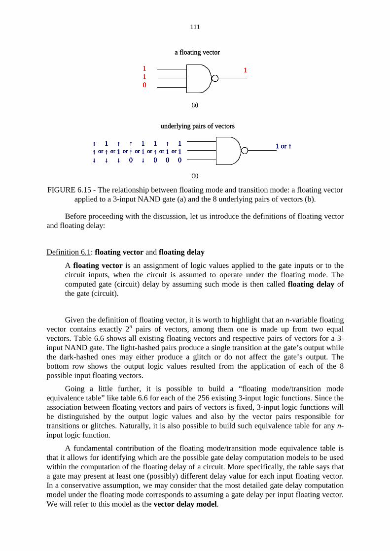
111
a floating vector
110
1
(a)
underlying pairs of vectors
1 or ↑110
↑10
1↑0
↑↑0
11↓
↑↑↓
↑1↓
1↑↓
or oror oror or or
(b)
a floating vector
110
1110
1
(a)
underlying pairs of vectors
1 or ↑110
↑10
1↑0
↑↑0
11↓
↑↑↓
↑1↓
1↑↓
or oror oror or or1 or ↑1
10
↑10
1↑0
↑↑0
11↓
↑↑↓
↑1↓
1↑↓
or oror oror or or110
↑10
1↑0
↑↑0
11↓
↑↑↓
↑1↓
1↑↓
or oror oror or or
(b)
FIGURE 6.15 - The relationship between floating mode and transition mode: a floating vectorapplied to a 3-input NAND gate (a) and the 8 underlying pairs of vectors (b).
Before proceeding with the discussion, let us introduce the definitions of floating vectorand floating delay:
Definition 6.1: floating vector and floating delay
A floating vector is an assignment of logic values applied to the gate inputs or to thecircuit inputs, when the circuit is assumed to operate under the floating mode. Thecomputed gate (circuit) delay by assuming such mode is then called floating delay ofthe gate (circuit).
Given the definition of floating vector, it is worth to highlight that an n-variable floatingvector contains exactly 2n pairs of vectors, among them one is made up from two equalvectors. Table 6.6 shows all existing floating vectors and respective pairs of vectors for a 3-input NAND gate. The light-hashed pairs produce a single transition at the gate’s output whilethe dark-hashed ones may either produce a glitch or do not affect the gate’s output. Thebottom row shows the output logic values resulted from the application of each of the 8possible input floating vectors.
Going a little further, it is possible to build a “floating mode/transition modeequivalence table” like table 6.6 for each of the 256 existing 3-input logic functions. Since theassociation between floating vectors and pairs of vectors is fixed, 3-input logic functions willbe distinguished by the output logic values and also by the vector pairs responsible fortransitions or glitches. Naturally, it is also possible to build such equivalence table for any n-input logic function.
A fundamental contribution of the floating mode/transition mode equivalence table isthat it allows for identifying which are the possible gate delay computation models to be usedwithin the computation of the floating delay of a circuit. More specifically, the table says thata gate may present at least one (possibly) different delay value for each input floating vector.In a conservative assumption, we may consider that the most detailed gate delay computationmodel under the floating mode corresponds to assuming a gate delay per input floating vector.We will refer to this model as the vector delay model.

112
TABLE 6.6 - Relationship between floating model vectors and transition model vectors.
input vector 000 001 010 011 100 101 110 111
000 001 010 011 100 101 110 111
↓00 ↓01 ↓10 ↓11 ↑00 ↑01 ↑10 ↑11
0↓0 0↓1 0↑0 0↑1 1↓0 1↓1 1↑0 1↑1
00↓ 00↑ 01↓ 01↑ 10↓ 10↑ 11↓ 11↑
↓↓ 0 ↓↓ 1 ↓↑ 0 ↓↑ 1 ↑↓ 0 ↑↓ 1 ↑↑ 0 ↑↑ 1
↓0↓ ↓ 0↑ ↓1↓ ↓1↑ ↑ 0↓ ↑ 0↑ ↑1↓ ↑1↑
0↓↓ 0↓↑ 0↑↓ 0↑↑ 1↓↓ 1↓↑ 1↑↓ 1↑↑
underlying pairs
of vectors
↓↓↓ ↓↓↑ ↓↑↓ ↓↑↑ ↑↓↓ ↑↓↑ ↑↑↓ ↑↑↑
output logic value 1 1 1 1 1 1 1 0
A less accurate, but still correct gate delay computation model corresponds to groupingthe input floating vector situations according to the transition type taking place at the gates’output. Thus, the gate will be assigned with a falling delay, taken from the delays of thosevectors that cause a falling output transition, and a rising delay, whose value comes from thevectors producing a rising output transition. This corresponds to a pair of separate fall/risedelay model.
A third gate delay computation model corresponds to assigning a single delay per gate,thus being called single delay model. Naturally, this is the most crude delay model, althoughcorrect from the floating delay computation’s point of view.
It is important to remark that, in order to get a robust floating delay computation, thegate delay values considered in each of the three models must represent an upper bound on thedelay of that gate for all instances of a whole circuit family. This means that the adoptedphysical delay model or component delay estimation method must furnish worst-case delayvalues for each circuit component.
A more careful analysis of table 6.6 allows us to conclude that the pin-to-pin delayformat normally used in standard-cell characterization is not appropriate for floating delaycomputation since this kind of model takes into account only a part of all input pairs ofvectors that may cause a transition at the gate’s output. For instance, in the case of a 3-inputgate, the pin-to-pin delay format would cover only six pairs of vectors: ↓11, 1↓1, 11↓ , ↑11,1↑1, 11↑ . That is, only single input transition situations.
A second contribution of the floating mode/transition mode equivalence table is that itlists all pairs of vectors underlying a given floating vector. Such information is useful forcarrying out the delay characterization of a gate through simulation. In this case, only thosepairs of vectors able to produce a transition at the gate output need be simulated. This mayreduce significantly the number of cases to be simulated: in the case of a 3-input NAND gate,only 26 cases from a total of 64. On the other hand, if gate delays are obtained through anyanalytical formulation, this information may be used to calibrate or to adapt the delaymodeling formulae in order to cover only the floating vector pairs of interest.

113
6.3.3 Gate Delay Computational Models and Timed Forward Implication for SCCGs
Table 6.6 allows us identifying all pairs of vectors that influence on the delay of a giveninput-floating vector, in the case of a 3-input NAND gate. However, thus far it was notmentioned the criterion to determine the gate delay value itself under the considered input-floating vector. Of course, whatever this criterion is, it is necessary to guarantee thecorrectness of the delay computation procedure (see section 2.6), that is, it is necessary toguarantee that the delay computation procedure provides a safe upper bound on the circuitdelay. Therefore, let us examine what are the circumstances leading to the safe upper boundfloating delay for the timed-test generation procedure.
As already explained, the timed-test generation procedure operates on a single primaryoutput at a time. Given a delay value δ and a logic value lv (0 or 1), it will result in success ifit is possible to justify lv at the primary output with lower delay greater than or equal δ. Thus,a success means that the delay at the considered primary output is never less than δ for lv. Onthe other hand, if it is not possible to justify lv at the primary output, or if it is possible tojustify it but the upper bound on the delay is strictly less than δ, then the procedure results infail. Figure 6.16 illustrates these two situations.
success
lv
lower_d upper_d
δ
lv
lower_d upper_d
δ
(a) (b)
failsuccess
lv
lower_d upper_d
δ
lv
lower_d upper_d
δ
(a) (b)
lv
lower_d upper_d
δ
lv
lower_d upper_d
δ
lv
lower_d upper_d
δ
lv
lower_d upper_d
δ
lv
lower_d upper_d
δ
lv
lower_d upper_d
δ
(a) (b)
fail
FIGURE 6.16 - Success (a) and fail (b) conditions for the timed-test generation procedure.
Given a multi output circuit and a delay value δ, if the timed-test procedure results infail for both 0 and 1 logic values for each primary output, then the next step for searching thecircuit floating delay is to guess a new δ, smaller than the previous one and restart to test eachprimary output. At this point, it is assumed with 100% of certitude that the circuit floatingdelay is less than the already tested δ. This certitude must be assured, whatever the modelsused are.
This way, the criterion for determining the delay of a gate under a given floating vectormust reinforce the previous premise. Considering the whole process of determining thefloating delay of a circuit with the timed-test generation procedure, a safe upper boundestimate is associated to the action of avoiding decreasing the value of δ whenever theaccuracies of the underlain models are questionable. Indeed, this is exactly the case: we arelooking for a criterion that allows determining the floating delay of a gate from a set ofpossible transition delays. Hence, it seems to be logical that for determining the floating delayof a gate one should take the greatest value among all transition delays associated to a givenfloating input vector because this may contribute to shift right both lower and upper delays atcircuit nodes with respect to the time axis. Shifting right delay bounds, by its turn, is a

114
conservative action because it increases the chances of the timed-test generation to return asuccess. Due to the already posed arguments, the delay of a gate under a given input-floatingvector must correspond to the maximum among the delays caused by the pairs of vectorsunderlying such floating vector.
On the other hand, the separate fall/rise delay model corresponds to an approximation ofthe vector delay model in which all floating vectors causing the same logic value at the gateoutput are grouped together. As a consequence, a gate may exhibit as many different delaysfor a given (output) logic value as the number of floating vectors that cause this logic value.Since we have already been conservative in determining floating vector delays, one mayimprove the gate delay computational model by considering a pair of delays for each logicvalue instead of a single value per logic value. To do that, each logic value 0 and 1 is assumedto have a maximum and a minimum delay value, taken from the slowest and fastest floatingvectors that cause the logic value, respectively. The minimum value is added to the lowerdelay bound, while the maximum value is added to the upper delay bound. Using the samearguments, the single delay model may be transformed into a pair of delays model in which amaximum and a minimum delay values are assumed.
Once we have derived safe rules for determining the delay of gates under any of thethree gate delay computation models, it is necessary to consider the application of such ruleswhile computing the lower and upper bounds of a gate within a forward implicationprocedure. Recalling the rules of the three-valued timed calculus described in tables 6.4 and6.5, the input floating vector situations that may occur can be classified according to thefollowing three groups:
1. Cases in which at least one of the inputs of g presents a controlling value (c(g)). Theothers may present either non-controlling values (nc(g)) or the 2 value;
2. The case in which all inputs of g present non-controlling values (nc(g));3. Cases in which at least one of the inputs of g presents a 2 value, but none presents a
controlling value (c(g)). The others may present non-controlling values (nc(g)).Groups 1 and 3 refer to cases where one of the gate inputs may present a 2 value. Within
the three-valued calculus, a 2 represents the existence of either logic value 0 or logic value 1.Thus, we may introduce the definition of a floating cube as follows.
Definition 6.2: floating cube
Given the three-valued calculus, a floating cube is an assignment of logic values, beingat least one of such values equal to 2. The number of floating vectors underlying afloating cube is 2m, where m is the number of positions presenting the value 2.
Indeed, a floating cube contains at least two floating vectors and thus can be viewed as avariation of the separate fall/rise delay model. In order to guarantee maximum accuracy, it isnecessary to consider the maximum and the minimum delay values for a cube. By doing this,the delay of a cube has an invariant form, independently on the gate delay computation modelused. To understand this, consider that the floating cube 022 is applied to the SCCG of figure
6.17, which logic function is CBAS ⋅+= . Table 6.7 shows the equivalence betweenfloating and transition modes for such gate. Note that this gate evaluates to 1 for floatingvectors 000, 001, 010 and evaluates to 0 for floating vectors 011, 100, 101, 110, 111. Ifthe delay computation procedure has assumed the vector delay model, then the delay of thisSCCG under cube 022 will present maximum and minimum values given by

115
maxd(000),d(001),d(010),d(011) and mind(000),d(001),d(010),d(011), respectively,where d(000), d(001), d(010) and d(011) are the delays of floating vectors 000, 001, 010 and011. On the other hand, if the delay computation procedure has assumed the separate fall/risedelay model, the maximum and minimum values are given by maxtpLHmax , tpHLmax andmintpLHmin , tpHLmin. However, for this SCCG, tpLHmax=maxd(000),d(001),d(010) andtpLHmin=mind(000),d(001),d(010), while tpHLmax=tpHLmin=d(011), which results the samemaximum and minimum delay values as in the floating vector delay model case. Byequivalent arguments, we may claim that the floating delay of this cube under the pair ofdelays model will result in the same maximum and minimum delay values computed for theother two gate delay models.
underlying floating vectors
a floating cube
022
2
0 or 1000
001
010
011
or or or
(a)
(b)
underlying floating vectors
a floating cube
022
2022
2
0 or 1000
001
010
011
or or or 0 or 1000
001
010
011
or or or000
001
010
011
or or or
(a)
(b)
FIGURE 6.17 - Delay of a SCCG under a floating cube.
TABLE 6.7 - Equivalence between floating and transition modes for the SCCG of figure 6.17.
input vector 000 001 010 011 100 101 110 111
000 001 010 011 100 101 110 111
↓00 ↓01 ↓10 ↓11 ↑00 ↑01 ↑10 ↑11
0↓0 0↓1 0↑0 0↑1 1↓0 1↓1 1↑0 1↑1
00↓ 00↑ 01↓ 01↑ 10↓ 10↑ 11↓ 11↑
↓↓ 0 ↓↓ 1 ↓↑ 0 ↓↑ 1 ↑↓ 0 ↑↓ 1 ↑↑ 0 ↑↑ 1
↓0↓ ↓0↑ ↓1↓ ↓1↑ ↑0↓ ↑0↑ ↑1↓ ↑1↑
0↓↓ 0↓↑ 0↑↓ 0↑↑ 1↓↓ 1↓↑ 1↑↓ 1↑↑
underlying pairs
of vectors
↓↓↓ ↓↓↑ ↓↑↓ ↓↑↑ ↑↓↓ ↑↓↑ ↑↑↓ ↑↑↑
output logic value 1 1 1 0 0 0 0 0
Analyzing again any equivalence table, it is possible to affirm that the delay of any gatedepends only on the cube (or vector) applied to its inputs. Particularly in the case of the

116
separate fall/rise delay model, we can affirm that the delay of a gate may be perfectly definedby the group(s) to which the input floating vector (cube) belongs. This conclusion ratifies theassumption of splitting the timed-value computation of a gate into two independent subtasks:
• The computation of the gate output logic value and the first-order delay bounds
• The identification of the floating delay of the gate, used to calculate the actual delaybounds.
From this verification, it becomes clear that the modifications needed to allowcomputing the timed-value of arbitrary complex gates, including SCCGs, were alreadycovered. These involve:
1. The function tree and the appropriate procedures for computing the gate output logicvalue and the first-order delay bounds;
2. The use of one of the three derived gate delay computation models (vector delay,pair of delays and single delay) to compute the lower and upper bounds on gateoutput delay.
6.3.4 Timed Backward Implication for SCCGs
The extended three-valued timed calculus detailed in the previous subsection allows forperforming forward implication on complex gates. However, the timed-test generationprocedure also has to perform backward implication during its execution. Thus, it is necessaryto investigate how to deal with complex gates while performing backward implication.
Given a gate, logical backward implication consists of finding an input assignment withrespect to this gate that sets its output to the desired logic value. Obviously, the desired outputlogic value is a known value, i.e., either a 0 or a 1. A conflict occurs when a given gate output
that presents logic value lv is required to have logic value lv .
In the case of timed backward implication, it is not sufficient to check for logicalconflicts. It is also necessary to check whether the lower and upper bounds on the delayrequired to each input are within the already set lower and upper bounds for the given input.Given a simple gate and a desired logic value at the gate’s output, the original timed-testgeneration procedure searches for the cube able to set the gate output to the desired logicvalue by exploiting the concept of controlling and noncontrolling values. Consider that a logic0 is to be set at an AND gate. Since 0 is the controlling value of an AND gate, there may existvarious possible vectors able to set the gate output to 0. Thus, the procedure searches for thefastest gate input able to be set to logic 0. If such input does not exist, then it is not possible tobackward the logic 0 through the considered gate.
In the case of complex gates, the concept of controlling and noncontrolling valuescannot be directly applied. However, we may realize that backward implying a logic valuethrough a gate is in fact a kind of “guessing procedure”, in which we are asked to find anassignment of input values that cause the desired output values. In this sense, it is obvious thatany backward implication procedure able to treat complex gates is indeed a generalization ofthe simple gate case.
The basic heuristics used by the timed-test generation procedure for performingbackward implication on simple gates relies on setting the smallest number of inputs because

117
such procedure results in a potentially smaller number of circuit lines that will have to bejustified. Thus, it is necessary to perform a systematic exploration of the local Booleansubspace (i.e., the Boolean space associated to the logic function implemented by the gateunder consideration), and at the same time, setting one input variable at a time.
The reasoning developed in the two last paragraphs suggests the possibility of using asystematic input space enumeration procedure along with the three-valued timed calculuspresented in table 6.6 to accomplish the logical backward implication on complex gates.Figure 6.18 exemplifies the backward implication procedure when a logic 0 is desired at theoutput of the SCCG of figure 6.17. In order to do that, we begin by setting the topmost inputto 0. Forward implication of this assignment results in a 2 at the SCCG output (figure 6.18a).This means that it is necessary to set one or more inputs. Assigning a 0 value to the middleinput results in logic 1 at the SCCG’s output (figure 6.18b), which is a conflict. Thus, webacktrack this assignment and replace de 0 by 1. The forward implication of this newassignment results in a 2 at the SCCG’s output (figure 6.18c). Setting the bottom most inputto 0 results in logic 1 at the output (figure 6.18d), which is also a conflict. Finally, bychanging the bottom input to logic 1 results the desired logic 0 at the gate output.
022
2
(a)
002
1
(b)
012
2
(c)
010
1
(d)
011
0
(e)
022
2
(a)
002
1
(b)
022
2
(a)
022
2022
2
(a)
002
1
(b)
002
1002
1
(b)
012
2
(c)
010
1
(d)
012
2
(c)
012
2012
2
(c)
010
1
(d)
010
1010
1
(d)
011
0
(e)
011
0011
0
(e)
FIGURE 6.18 - Backward implication in a SCCG by using forward implication rules.
The previously described solution for backward implication of complex gates isequivalent to the PODEM algorithm applied to a single gate, but with significantly smallertime complexity, since we restrict the number of inputs for complex gates. However, the mostimportant aspect on such procedure is that it may use the three-valued timed rules andfunction tree already developed. The only extra resource needed is an enumerationmechanism, for controlling the subspace exploration.
Having found a procedure for performing logical backward implication on complexgates, let us now move to the timed backward implication. Similarly to the timed forwardimplication, we will split the procedure into two steps:
1. Logical backward implication
2. First-order delay bounds computation and conflict detection.

118
The first step has already been described. The second one is composed of the followingsub-steps, by the order:
1. Determine the gate delay under the selected input cube k (i.e., gate input assignment)
2. From the output lower and upper bounds, computes the first-order lower and upperbounds for each gate input by using the formulae: lo’=lo-d(kmax) and uo’=uo-d(kmin),where d(kmax) and d(kmin) are the maximum and minimum delays for cube k assignedto the gate inputs, respectively.
3. For each gate input i, compute the intersection between the input lower and upperdelay bounds and the first-order lower and upper delay bounds computed in theprevious step.
In step 3, a conflict is detected if lo’<li or if uo’<ui. Note that a gate input may provoke aconflict even if its logic value is 2.
Once timed forward and backward implication procedures able to handle complex gateshave been developed, the timed-test generation procedure has been made sufficiently generalto treat circuits containing complex gates.
It is important to notice that the proposed method to perform the three-value timedcalculus on complex gates does not represent a significant increase in the overall executiontime because macrocell generators are generally not allowed to generate complex gates withmore than five serial transistors, due to technological reasons.

119
7 Conclusions
This thesis was concerned with the functional timing analysis (FTA) of combinationalcircuits, with emphasis to the applicability of FTA algorithms and models to circuitscontaining complex gates. Contributions were given to both FTA general theory and to FTAof circuits containing complex gates.
As a fundamental contribution, it was provided probably the deepest systematic study ontiming analysis models and algorithms ever found in the literature. In order to facilitate thecomprehension of the whole scenario, a new taxonomy for classifying FTA algorithms wasproposed. According to this taxonomy, FTA algorithms may be classified with respect to thenumber of paths simultaneously handled in sensitization tests (single path sensitization,concurrent path sensitization or mixed approach), with respect to the method used todetermine whether sensitization conditions are satisfiable or not (ATPG-based, SAT-based orother) and with respect to the sensitization criterion itself.
Still within the FTA theory, it was claimed that synchronous circuits implemented withcurrent fabrication technologies might present an asynchronous behavior that cannot beproperly captured by the transition delay model. It means that, in order to avoidunderestimating the circuit delay, one would rather compute the delay under sequences ofvectors than the delay under pairs of vectors. On the other hand, the floating delay model isthe only one able to provide a safe upper bound on the circuit delay under sequences ofvectors. As long as the floating delay model is the delay model underlying FTA, this is astrong argument to justify the use of FTA as the timing verification method.
Experimental results on path enumeration procedures presented in appendix 2confirmed the severity of the so-called “path explosion problem” faced by the single pathsensitization method. Due to this, concurrent path sensitization methods (either ATPG-basedor SAT-based) represent the state-of-art in FTA algorithms.
Concerning FTA with complex gates, the TrueD-F algorithm proposed by Devadas et al.was chosen for serving as basis of an ATPG-based concurrent path sensitization techniquethat deals with circuits containing complex gates without requiring macro-expansion. Thechoice of the ATPG-based approach was motivated by the problems exhibited by the SAT-based approach when more realistic delay models are used. Another argument for choosingthe ATPG-based approach is the existence of several acceleration techniques for ATPGalgorithms.
The most important contribution of this thesis to FTA with complex gates concerns theextension of the timed-calculus to complex gates. Within the TrueD-F algorithm, the timedcalculus consists of a set of rules used to compute logic values at gates and the related lowerand upper bounds on delay. According to the proposed method, the computation of the timed-value of a complex gate may be accomplished by a recursive procedure that evaluates eachsub-tree, beginning from the leaves. For a maximum of 4 serial transistors in both PMOS andNMOS networks, the maximal number of sub-trees that any SCCG may exhibit is 11,including the topmost one. Considering that the evaluation of a single sub-tree consists of asimple computation of delay intervals and logic values over the involved inputs, one canexpect that operating directly on complex gates can lead to execution times that are at mostequivalent to those necessary to perform the timed-value computation on an equivalent

120
macro-expanded network. However, it is worth to mention that applying an ATPG-basedalgorithm to an equivalent macro-expanded network may lead to significant overhead inexecution time due to the potential increase in the number of circuit lines to be justified.
Other important contributions to the FTA with complex gates resulted from theinvestigation of the computational delay models applicable to the complex gates’ case. Thefloating mode/transition mode equivalence table identifies the pairs of vectors underlying eachfloating vector. It also leads to the identification of the three valid gate delay computationmodels under the floating circuit delay model. These are the vector delay, the separate fall/risedelay and the single delay. Although being the most accurate, the vector delay model requiresa delay value (or a pair of values) for each 2n floating vectors, where n is the number of inputsof the gate. Considering SCCGs with no more than 4 serial transistors, the maximal n is 16,which gives a total of 216= 65536 floating vectors. On the other hand, the separate fall/risedelay model groups all floating vectors into two cases, thus reducing the delay values of a gateto two (or two pairs), while still assuring an upper bound on the gate delay.
The identification of the pairs of vectors underlying a given floating vector is of greatinterest when gate delay characterization is to be performed. In case of electrical simulation,only the vector pairs that may cause an output transition must be considered. In case of delaycharacterization by analytical formulation, this information may be used to adapt the delaymodeling formulae in order to cover only the vector pairs of interest. However, identifying allpairs of vectors of interest for gates with many inputs constitutes a very hard task that must befurther investigated. On the other hand, a very important conclusion that can be stated fromthe equivalence table is that the pin-to-pin delay format normally used in standard-cellcharacterization may result in an underestimation of gate delay since it takes into account onlya part of all input floating vectors that may cause a transition at gate’s output.
Finally, from the floating mode/transition mode equivalence table it was possible tointroduce the concept of floating delay of a cube, as a generalization of the vector delaymodel.
Timed forward implication for complex gates is accomplished by using the procedurethat computes the timed-value of gates. As already argued, the resulted time complexity isexpected to be at most equivalent to that resulted from working on an equivalent macro-expanded network. Timed backward implication with complex gates, by its turn, cannot bedirectly derived from backward implication with simple gates because the concepts ofcontrolling/non-controlling values are not applicable to complex gates. Thus, the proposedmethod relies on using the same procedure that computes the timed-value in forwardimplication, but in a PODEM-like fashion, by using input cube simulation on each gate. Inputcube simulation presents a worst-case execution time that is proportional to the input space ofthe gate. For instance, the input space of a SCCG with 4 serial transistors in both networks hasat most 216= 65536 floating vectors. Of course, this affects the execution time of the overallFTA algorithm.
This thesis showed that it is possible to perform ATPG-based concurrent pathsensitization FTA of circuits containing complex gates without macro-expanding complexgates. The main advantage of such approach is the potential reduction in the number of circuitlines that must be justified, with comparison to the approach that uses macro-expansion.Nevertheless, the complexity of backward implication is significantly increased mainly whencomplex gates with many inputs are present in the circuit. This problem may be alleviated bythe use of testability measures to guide the gate input space exploration.

121
Finally, the proposed extended timed calculus along with the complex gate delay validmodels form a set of macro-modeling rules that make possible to perform “hierarchicalfloating delay computation”. This is a consequence of the fact that complex gates are thecorrect generalization of the smallest portion of any CMOS network.
7.1 Future Work
The performance of the proposed approach is greatly dependent on the ability of makingright decisions. Such quality can be attained by making use of testability measures, as done inPODEM and FAN algorithms. Thus, the computation of testability in circuits with complexgates is a point to be addressed in short term.
The studies on valid gate delay computation models helped to fill the gap existingbetween physical and computation delay models. There are several points deserving attention,however. One of them is the (automatic) identification of the pairs of vectors responsible fortransitions at gates’ outputs. Another one is the gate delay characterization itself. This latterone involves either electrical simulation or analytical characterization, but both respecting thevalid gate delay floating models. A third one concerns the maximal number of inputs ofcomplex gates, which directly influences the performance of the proposed ATPG-based FTAmethod. The number of inputs in complex gates is also responsible for preventing the use ofthe floating vector delay model, which is the most accurate. Limiting the number of serialtransistors to 4 is a commonly used design strategy that assures reasonable electricalperformance for SCCGs, but still leads to a total of 3503 possibilities of SCCGs. A veryuseful work consists on investigating the actual capabilities of state-of-art technologymapping algorithms in order to determine a practical limit on the number of inputs of SCCGs.
The proposed approach must be compared to the macro-expansion approach both interms of performance and in accuracy, to certify that the reduction in the number of lines to bejustified overcomes the increase in complexity of timed forward and backward implicationprocedures.
Investigating the accuracy and the performance of hierarchical floating delaycomputation is also a very important work. It seems to be clear that the acceleration obtainedby the hierarchical mode may allow FTA of circuits with at least one or two orders ofmagnitude. However, it is necessary to investigate the impact of the gate delay computationmodel on the resulted accuracy.
Last, but also quite important, is a broad comparison between the SAT-based approachand the proposed one, which is an ATPG-based approach. One basic difficulty relies onselecting a set of delay computation models that are valid on both cases and at the same timeare able to provide delay estimates with acceptable accuracy. Another difficulty relies onchoosing an existing SAT-based tool (or algorithm) able to deal with complex gates.

122

123
Appendix 1 The Need for Functional Timing Analysis: aCase Study
Concerning delay computation techniques and algorithms, a question that frequentlyarises is whether it is worth to perform FTA, since the computational effort is significantlygreater than in TTA case. Obviously, this would be quite simple to answer if one could alwaysassure to have total control over the design under development. However, due to theincreasing complexity of current VLSI designs and to the use of EDA tools, it is not possiblefor the designer to know all details of each design. Thus, since TTA and FTA may providedifferent delay estimates for the same circuit, it is important to measure how severe thisdifference can be and what would be its impact in the maximal operating frequencyestimation.
There are some classes of combinational circuits that have been extensively used toillustrate the effect of disregarding the influence of path sensitization in delay estimation.Carry-skip adders (csas) constitute one such class for it is well known they may containhundreds of thousands of false paths [LAM94][DEV94]. Although in the case of csas thedifference between the delay estimated by TTA and the delay estimated by FTA may representan extreme case, it is still necessary to consider that for automatically generated designs thisdifference may also be significant.
In order to evaluate the difference between TTA and FTA estimations originated fromconsidering or not path sensitizability, a discussion on delay estimation of csas is carry out inthe sequel. To be more realistic, a non-unitary component delay model is used [DAG96].
Figure A1.1 reproduces the 2-bit csa showed in figure 2.4. This csa2 has been mappedusing simple CMOS gates (in this case, 2-input nands and inverters). Assume a fixed gatedelay computation model with separate falling and rising delays. In order to construct higherorder adders, csa2 stages are connected together through the carry in/carry out pins, as shownin figure A1.2. Thus, a practical approach for estimating the delay of higher order csas is firstcharacterize a single csa2 stage and then use the results of this characterization to infer thewhole circuit delay.
If TTA is the chosen method, then the circuit delay is found by identifying the longesttopological path, which is clearly the carry chain.
However, if FTA is the computation method to be used, then it will be necessary toidentify the longest path able to propagate a transition. This means that path sensitizabilitymust be considered. The fact that the only connection between two adjacent stages in higherorder csas is through the carry chain suggests the classification of stages into three groups[GÜN99a]:
• first stage
• intermediate stages
• last stage
For each of these three cases an ad hoc sensitization analysis is then performed. It is alsopossible to take advantage on the regularity exhibited by csas: all analyses may be performedover the same csa2 instance. In order to facilitate the analyses, the transition mode will be

124
assumed (see section 2.3). The error of such assumptions may not be significant in the specificcase of csas.
a0
c0
b1
a1
b0
p0
p1
g0
g1
s0
c2
s1
n0
ctrl_n
n1n2 n3
mux2-1
n4
n5
FIGURE A1.1 - A 2-bit carry-skip adder (csa2) mapped using 2-input nands and inverters.
The target of the sensitization analysis of the first stage is to find the pair of longestsensitizable paths beginning at any primary input and ending at output c2, being oneresponsible for a falling transition at c2 and the other responsible for the rising transition atc2.
For an intermediate stage, the target is to find the pair of longest sensitizable pathsbeginning at c0 and ending at c2, with one of the paths beginning by a falling transition (at c0)and the other beginning by a rising transition at (c0).
Finally, the analysis of the last stage is to find the pair of longest sensitizable pathsbeginning at c0 and ending at any output, where one of the paths begins with a fallingtransition (at c0) and the other begins with a rising transition at (c0).
The longest sensitizable path is then determined by summing the delay of all stages,taking into account signal polarity. Note that the described method allows for performing anapproximate hierarchical FTA without enumerating circuit paths.

125
first stage
last stage
intermediatestages
possible critical paths
csa20
a1b1 a0b0 c0
c2s1 s0
csa21
csa22
csa23
c4
c6
c8 s7 s6
s5 s4
s3 s2
a3b3 a2b2
a5b5 a4b4
a7b7 a6b6
FIGURE A1.2- An 8-bit carry-skip adder made of csa2 stages.
Consider an intermediate csa2 stage. There are only two topological paths between c0and c2. Each topological path may be divided into two logical paths, being one associated tothe falling transition (at its input) and the other associated to the rising transition (at its input).Thus, for an intermediate stage, the logical paths of interest are P0↑=(↑c0, n0, n1, n2, n3, n4,c2), P0↓=(↓c0, n0, n1, n2, n3, n4, c2), P1↑=(↑c0, n5, c2) and P1↓=(↓c0, n5, c2), whichdelays are 1204ps, 1134ps, 546ps and 482ps, respectively.
The ad hoc analysis will try to determine whether P0↑ is sensitizable or not by checkingall possible conditions that may activate it. If it is not possible to find a set of signalconditions that activates P0↑ , then P1↑ will be analyzed. The search of a sensitizable logicalpath beginning with a falling transition will also follow the path delay order: P0↓ and thenP1↓ . To reduce the search space, the check begins by setting stable logic values (either 0 or 1)to circuit nodes whenever possible. Otherwise, 0→1 and 1→0 transitions will have to beconsidered, along with the required stable times. Of course, the second possibility increasesthe analysis complexity, and thus should be avoided.
Figure A1.3 shows a set of signal conditions for trying to sensitize P0↑ : inputs a0 andb0 have been assigned to static values in such a manner that both p0 and g0 have a static 1.This allows a transition to propagate from c0 to n0 and from n0 to n1. However, given theprevious conditions, it is not possible to assign static values to g1, p1, ctrl_n and n5 in orderto allow a transition to propagate from n2 to c2. Thus, it will be necessary to consider signaltransitions at g1, p1, ctrl_n and n5, along with the required stable times.9 In figure A1.3, thesedelay-dependent conditions are expressed in terms of inequations, annotated at the respectivesignals. By assembling appropriate inequation systems it is possible to determine whether asensitization condition exists or not for the path P0↑ :
9 Note that the analysis of any path in the intermediate stages (and also for paths in the last stage) must consider a possiblynon-zero arrival time of a transition applied to c0, to model the effect of previous csa2 stages.

126
↓p1 > 399 + ∆
↓p1 + 285 < 662 + ∆
and
↑p1 < 399 + ∆
↑p1 + 212 > 662 + ∆
By evaluating inequations A1.1 and inequations A1.2 one conclude that it is notpossible to find an arriving time value at input c0 (∆) that combined with either a falling or arising transition at node p1 (↓p1 or ↑p1) could result in a valid sensitization condition. Noneof the other possible signal assignments resulted in valid sensitization conditions. Thus, theconclusion is that path P0↑ is not sensitizable.
a0
↑0+∆
0 1
1 0
or
c0
b1
a1
b0
p0
p1
g0
g1
s0
1
c2
s1
n0
ctrl_n
n1n2
n3↓108+∆ ↑399+∆ ↓528+∆
1
↓>399+∆
↑<399+∆
↓>646+∆↑<646+∆
↑662+∆
↓766+∆
↑1204+∆
↓285↑212
?
FIGURE A1.3 - A set of signal conditions for trying to sensitize P0↑ .
Similar analyses on the other paths lead us to the conclusion that P1↑ and P1↓ are thesensitizable paths for any intermediate csa2 stage.
Applying the same procedure to the first csa2 stage we find that the longest sensitizablepaths generating a falling transition at c2 are P2↓=(↓a0, 4-X0, p0, n0, n1, n2, n3, n4, c2) andP3↓=(↓b0, 3-X0, p0, n0, n1, n2, n3, n4, c2), both with delay 1559ps. And the longestsensitizable paths generating a rising transition at c2 are P4↓=(↓a0, 1-X10, 3-X0, p0, n0, n1,n2, n3, n4, c2), P5↓=(↓b0, 2-X0, 4-X0, p0, n0, n1, n2, n3, n4, c2), P6↓=(↓a1, 1-X3, 3-X3, p1,ctrl_n, sel-X11, n5, c2) and P7↓=(↓b1, 2-X3, 4-X3, p1, ctrl_n, sel-X11, n5, c2), all of themwith delay 1435ps.
(A1.1)
(A1.2)

127
Finally, for the last csa2 stage, the longest sensitizable paths are P8↓=(↓c0, n0, n1, 2-X5, 4-X5, s1) and P9↑=(↑c0, n0, n1, 2-X5, 4-X5, s1), with delays of 1074ps and 998ps,respectively.
The delay values obtained from the sensitization analysis should be combined to derivegeneral formulae to approximate the delay of csa adders made up from the analyzed csa2stage. The formulae will give approximate values because they do not account for themodifications on gate delays arriving from the new fanin/fanout relations when csa2 stagesare connected together. The equations that approximate the (output) falling and the risingcritical delays of csa adders are:
433222
m465tdmax +
−×↓= [ps] (A1.3)
263322
m824tdmax +
−×↑= [ps] (A1.4)
where m ∈ (4,8,16,..), corresponding to 4-bit, 8-bit, 16-bit csa adders. To estimate the criticaldelay of a given adder (csa4, csa8 etc), equations A1.3 and A1.4 must be evaluated. Thecritical delay will be given by max(tdmax↓ ,tdmax↑ ).
And the equations that approximate the (output) falling and the rising topological delaysare:
605112
m1134tdmax +
−×↓= [ps] (A1.5)
766112
m2041tdmax +
−×↑= [ps] (A1.6)
Similarly, the topological delay of a given adder is given by max(tdmax↓ ,tdmax↑ ), wheretdmax↓ and tdmax↑ are obtained through equations A1.5 and A1.6. The estimations for 2, 4, 8,16, 32 and 64-bit adders are shown in table A1.1.
TABLE A1.1 - Critical delay estimations for csa adders.
adder topologicaldelay (ps) (1)
criticaldelay (ps) (2)
(1)/(2)
csa2 1766 1560 1.13csa4.2 2970 2633 1.12csa8.2 5378 3597 1.49csa16.2 10194 5709 1.78csa32.2 19826 10077 1.96csa64.2 39090 18813 2.07
The results of table A1.1 show that in case of adders built up from the analyzed csa2 thedifference between the topological delay and the critical delay (i.e., the delay obtained bytesting path sensitizability) may be significant. In the case of csa64.2, for instance, thetopological analysis has overestimated the delay by 100%. This means that the clockfrequency obtained through a topological analysis could still be speeded up by a factor of 2!

128
The previous results illustrate the importance of considering path sensitization in timinganalysis. And although the carry-skip adder case would represent a very particular class ofcircuits, there are other important classes of circuits exhibiting significant difference betweenthe topological delay and the (actual) critical delay.

129
Appendix 2 Gate Delay Computation Models and theComplexity of Best-First Search Procedures
The crudest gate delay computation model that can be used in a FTA tool is the singlefixed delay that assigns one delay value per gate. The target of the following discussions isinvestigating the computational effort necessary to use a pair of delays per gate within best-first search path enumeration procedures. Throughout this discussion, the referred gate delaymodels were renamed to single gate delay (sgd), which assumes only one delay per gate, andsingle pair gate delay (spgd), which considers a pair of delays per gate, being one for thefalling (output) transition and another for the rising (output) transition [GÜN98a][GÜN98b].
In order to investigate the relevance of using the spgd method in path enumeration(instead of the sgd method), it was initially considered the problem of finding the longest(topological) path of the CMOS gate chains listed in table A2.1. These chains are eithersingle-type (i.e., containing only one type of CMOS gate) or multiple-type (i.e., containingmore than one type of CMOS gate). All chains have 20 gates. Note that in the sgd case, thedelay of a path is computed simply by adding the delay of each gate along the path, accordingto equation 5.1. However, in the spgd, each topological path originates two logical paths,possibly with distinct delays calculated by equations 5.5 and 5.6.
TABLE A2.1 - List of CMOS gate chains used to evaluate sgd and spgd path delaycalculations.
chain description
p_nand2 2-input nand chainp_nand3 3-input nand chainp_nand4 4-input nand chainp_nor2 2-input nor chainp_nor3 3-input nor chainp_nor4 4-input nor chainp_nand3-4 chain with 3 and 4-input nandsp_nor3-4 chain with 3 and 4-input norsp_n3n4i chain with inverters, 3 and 4-input
nands and norsp_n3n4 3 and 4-input nands and nors
For estimating individual gate delays, a linear delay model was used. This model isassociated to the cells of a sea-of-gates library, developed in standard 0.8µm CMOStechnology. Although the linear delay model is not very accurate, it serves for the purpose ofcomparing the two methods under evaluation.
Considering that the adopted component delay model is able to furnish a pair of delaysper gate, the spgd method was used as reference to evaluate the loss of accuracy resulted fromusing the sgd method. To derive the delay of each gate v for the sgd case, three possibilitieswere considered [GÜN98]: td(v)=maxtdlh(v),tdhl(v), td(v)=(tdlh(v)+tdhl(v))/2 and

130
td(v)=mintdlh(v),tdhl(v), which will be referred as max, typical and min cases,respectively. Figure A2.1 shows the percent error resulted from using the sgd method (insteadof the spgd method) for the CMOS gate chains.
p_na
nd2
p_na
nd3
p_na
nd4
p_no
r2
p_no
r3
p_no
r4
p_na
nd3-
4
p_no
r3-4
p_n3
n4i
p_n3
n4
-60%
-40%
-20%
0%
20%
40%
60%
p_na
nd2
p_na
nd3
p_na
nd4
p_no
r2
p_no
r3
p_no
r4
p_na
nd3-
4
p_no
r3-4
p_n3
n4i
p_n3
n4
circuit
maxtypicalmin
FIGURE A2.1 - Percent error resulted from using the sgd method.
For all chains, max case overestimated the critical path delay up to 57%, while min caseunderestimated the critical path delay up to 57%. Typ case has presented no error for the first6 cases (from p_nand2 to p_nor4), which are single-type gate chains. For the remaining 4circuits, which are multiple-type gate paths, the error of typ case was within the range 3%-17%. Since in real-life digital designs it is not practical to avoid multiple-type gate paths, wecannot disregard the fact that typ case may underestimate the critical path delay.
Another aspect of relevance in the performance of best-first search path enumeration isthe type of data structures used to store partial paths. In the best-first procedure of Yen et al.[YEN89] k-list was originally described to be a static linear list used to store both partial andcomplete paths. At the beginning of the procedure it was initialized with partial paths, sortedby their esperances. After all partial paths had been extended k-list holds the k-most criticalpaths of the circuit. Thus, the procedure controls the total amount of memory to be allocatedby allowing only the first k paths to be traced and by using a static data structure. However, inpath-based FTA, i.e. single path sensitization algorithms, it is not possible to precisebeforehand how many paths must be traced until the first sensitizable one is found. In case theoriginal procedure is used, the absence of a sensitizable path within the k-most critical pathswill demand another run with a greater k. For circuits containing hundreds of thousands oflong unsensitizable paths, the need for re-running the enumeration procedure many times mayrender FTA impracticable.
In order to allow the procedure to stop by other criteria (e.g., when the first sensitizablepath is found), the data structure used in the modified best-first search procedure of subsection5.2.2 was mostly modified [PIN98][GÜN99]. For storing partial paths, two options of datastructures were made available: a dynamic linear list and a binary tree. During the wholeprocess of path enumeration partial paths are kept ordered by using the esperance value, as inthe original version of [YEN89]. In the binary tree case, a heapsort procedure [COR90] isused to maintain the order. Hence, the main feature of this “heapified” binary tree is that thepartial path having the greatest esperance is stored on its root. From now on, the two versionsof partial path lists are going to be referred to as linear and tree.

131
A second (linear) list called list_of_paths is used to store complete paths. This list doesnot require any special insertion scheme since the best-first procedure assures that paths aretraced in an ordered manner. Figure A2.2 depicts the possible data structures for storingpartial paths, along with the structure that stores complete paths.
partial paths list complete paths list
or
(Linear list)
Linear list (“linear version”)
Heaped binary tree (“tree version”)
FIGURE A2.2 - Data structures of the best-first procedure for path enumeration.
These later data structures gave rise to two versions of the best-first procedure, which,by they turn, could use either the sgd or the spgd path delay calculations [GÜN99]. Thus, fourversions of best-first enumeration procedure were available, as summarized in table A2.2.
TABLE A2.2 - Versions of the best-first procedure for path enumeration.
type of list for storingversion path delay calculationmethod complete paths partial paths
spg-linear spd dynamic linear dynamic linearspgd-linear spgd dynamic linear dynamic linear
spg-tree spd dynamic linear binary treespgd-tree spgd dynamic linear binary tree
The described versions of the best-first search based path enumeration algorithm wereimplemented using C language.
To evaluate the performance of the best-first search based path enumeration algorithmsthe circuits of the ISCAS’85 suite were used. These circuits were mapped using only simpleCMOS static gates (neither transmission gates nor CMOS complex gates were used). TableA2.3 shows the complexity of the DAGs that represent these circuits.

132
TABLE A2.3 - Complexity of the ISCAS’85 benchmark circuits.
circuit # of gates # of nets # of graph nodes # of graph edges
c432 182 222 231 448c499 364 405 439 883c880 529 589 617 987c1355 604 645 679 1227c1908 955 988 1015 1656c2670 1605 1762 1828 2773c3540 2307 2357 2381 3671c5315 3249 3427 3552 5752c6288 2672 2704 2738 5152c7552 4556 4762 4871 7608
The evaluation of the execution time was accomplished by running the algorithms on aSun Ultra2™ workstation with 256 Mbytes of RAM memory and 586 Mbytes of swapmemory for several values of k (number of paths traced). Execution times for linear versionwith k=10000 are showed in figure A2.3. From these results one can conclude that theexecution time of the linear version is greater than that of the tree version. Furthermore, thisdifference is significant for the most complex circuits. It is also possible to observe that forthe majority of the circuits the execution time of the spgd case is greater than the executiontime of the sgd case (for both linear and tree versions). This result was expected since thenumber of partial path insertions tends to be greater in the spgd case. However, the differenceis significant only for circuit c880 and c1355 (3.2 seconds and 7 seconds, respectively). For allother cases, the spgd-based procedure is at most 1 second slower.
0
10000
20000
30000
40000
50000
60000
c432 c499 c880 c1355 c1908 c2670 c3540 c5315 c6288 c7552
circuit
k=10000
sgd-linear
spgd-linear
sgd-tree
spgd-tree
FIGURE A2.3 - Execution times for k=10000 paths.
The time complexity of the best-first procedure is basically dominated by insertingpartial paths in the partial path list. Thus, reducing the partial path insertion time maysignificantly reduce the overall execution time. Indeed, the curves execution time x number oftraced paths showed by figure A2.4 confirm this supposition [PIN98][GÜN99]. It can be seen

133
that the time complexity of linear version is exponential with respect to k, while the timecomplexity of tree version is almost linear. As a result, the execution time overhead of thespgd method is greatly reduced by the use of the “heaped” binary tree.
Figure A2.5 shows the curves memory used x number of traced paths for the samecircuits of figure A2.3. It can be seen that in terms of memory use the behavior is exactly theopposite: the linear version presents linear dependency on the number of traced paths k, whilethe tree version presents exponential dependency.
c1908
0
2000
4000
6000
8000
10000
12000
14000
16000
18000
1 3 5 7 9 20 30 50 70 90
sgd-linear
spgd-linear
sgd-tree
spgd-tree
c1355
0
2000
4000
6000
8000
10000
12000
14000
16000
1 3 5 7 9 20 40 60 80 100
sgd-linearspgd-linearsgd-treespgd-tree
c2670
0
1000
2000
3000
4000
5000
6000
7000
8000
1 2 3 4 5 6 7 8 9 10 20 30 40 50 60 70 80 90 100
sgd-linearspgd-linearsgd-treespgd-tree
c3540
0
1000
2000
3000
4000
5000
6000
7000
8000
9000
1 2 3 4 5 6 7 8 9 10 20 30 40 50 60 70 80 90 100
sgd-linearspgd-linearsgd-treespgd-tree
FIGURE A2.4 - Curves execution time(ms) x number of traced paths for some ISCAS85circuits.
In a timing analysis tool that checks sensitizability, the tree version would be preferredbecause it is not possible to know a priori how many paths will be traced to find a sensitizableone. Thus, the use of a linear version (solely) would result in excessively long executiontimes. On the other hand, the tree version would not finish executing for circuits with toomany false paths, as the carry-skip adders studied in Appendix 1. The solution for this can bethe integration of both algorithms in a timing analysis tool, such that the user can choose thealgorithm she/he wants to use. Another possibility is to perform hierarchical timing analysis.But even in this case, enumeration-based timing analysis tools would have embedded one orboth discussed algorithms.
Let us now turn our attention to the applicability of the explicit enumeration method forperforming FTA of a real-life case. Consider again the carry-skip adders discussed inAppendix 1. As it was mentioned, the only connection between two adjacent csa stages isthrough logical paths P0↑ , P0↓ , P1↑ , or P1↓ . It was shown that both logical paths P0↑ andP0↓ are not sensitizable for the assumed gate delay assignment. Therefore, one could think oflogical paths P0↑ and P0↓ as being blocking trunks for any signal propagation throughadjacent csa stages and use this information to detect false paths in an explicit enumerationloop [GÜN99a]. In order to do this, the best-first search procedures previously described(spgd-linear and spgd-tree) were adapted: each time a new path is completely extended, a

134
checking procedure searches for the presence of any blocking logical trunk, which arepreviously furnished by the user, through an ASCII file. As long as paths are enumerated in anon-increasing order of delays, the first path not containing any blocking trunk is assumed tobe the critical path of the circuit.
c1908
0.00E+00
5.00E+12
1.00E+13
1.50E+13
2.00E+13
2.50E+13
3.00E+13
3.50E+13
4.00E+13
1 3 5 7 9 20 30 50 70 90
sgd-linear
spgd-linear
sgd-tree
spgd-tree
c1355
0.00E+00
2.00E+12
4.00E+12
6.00E+12
8.00E+12
1.00E+13
1.20E+13
1.40E+13
1.60E+13
1 3 5 7 9 20 40 60 80 100
sgd-linearspgd-linearsgd-treespgd-tree
c2670
0.00E+00
2.00E+12
4.00E+12
6.00E+12
8.00E+12
1.00E+13
1.20E+13
1.40E+13
1.60E+13
1.80E+13
1 3 5 7 9 20 40 60 80 100
sgd-linearspgd-linearsgd-treespgd-tree
c3540
0.00E+00
5.00E+12
1.00E+13
1.50E+13
2.00E+13
2.50E+13
3.00E+13
3.50E+13
1 3 5 7 9 20 40 60 80 100
sgd-linearspgd-linearsgd-treespgd-tree
FIGURE A3.5 - Curves memory used (bytes) x number of traced paths for some ISCAS85circuits.
Table A2.4 shows the approximate execution times for the semi-automaticunsensitizable path detection procedure for the carry-skip adders of Appendix 1. It has run onan Ultra10 SparcStation with 512Mbytes of physical memory. It is also showed the computedcritical delays and the number of traced paths until the first sensitizable path was found andthe approximate running time. The computed critical delays may differ from the calculatedones (also in Appendix 1) because in the semi-automatic procedure the fanout loads resultedfrom connecting two adjacent csa stages are considered in detail by the physical delaymodeler.
The execution times confirm the limitation of explicit path enumeration proceduresrunning in flat mode: the two most complex circuits did not complete due to the large numberof unsensitizable long paths. In the case of csa32.2, the enumeration tool has traced more than300 thousand paths without finding any sensitizable one!

135
TABLE A2.4 - Execution time for the semi-automatic unsensitizable path detectionprocedure.
adder topologicaldelay (ps) (1)
computeddelay (ps) (2)
# of tracedpaths
(1) /(2) executiontime (ms)**
csa2 1766 1560 7 1.13 30csa4.2 2970 2652 16 1.12 70csa8.2 5378 3654 786 1.47 680csa16.2 10194 5658 40190 1.80 157000csa32.2 19826 * - - -csa64.2 39090 * - - -
* Not finished after 24 hours.** Execution times for the spgd-linear procedure.
One advantage of the presented semi-automatic method is that it reduces the effortneeded to perform the ad hoc sensitization analysis, since only unsensitizable trunks must befound. Another advantage is the better accuracy obtained in delay calculation, when comparedto the calculation method proposed in section 3.4, since actual fanin and fanout are consideredin the delay calculation phase. As a counterpart, the method suffers from the path explosionproblem [MCG93], since the explicit path enumeration tool runs only on flat circuitdescriptions. It is interesting to remark that the spgd-tree version has presented memoryallocation problems that prevented its use for the largest circuits. On the other hand, the spgd-linear version has not presented memory problems, but execution time problems, since itcould not finish executing after 24 hours.

136

137
Appendix 3 Análise de Timing Funcional de CircuitosVLSI Contendo Portas Complexas
Este anexo apresenta um resumo estendido em português desta tese.
A verificação de timing tem como objetivo determinar se as restrições temporaisimpostas ao projeto podem ser satisfeitas ou não. De modo mais objetivo, a verificação detiming está relacionada com a estimativa do atraso crítico dos circuitos e com a máximafreqüência de operação. A precisão da verificação de timing depende da precisão dosmodelos adotados. Por modelos entende-se não apenas os modelos físicos de atraso usadospara quantificar o atraso de cada componente do circuito, mas também os modeloscomputacionais para os atrasos dos componentes e do circuito como um todo. Estes últimosestão relacionados ao modelo de operação do circuito, isto é, se o circuito opera no modosíncrono ou no modo assíncrono.
A maioria das técnicas de verificação de timing são orientadas a circuitos seqüenciaissíncronos. Desta forma, consideremos os aspectos mais importantes ao se estimar a máximafreqüência de operação de um circuito seqüencial que pode ser representado pelo modelo deMealy. O modelo de Mealy, mostrado na figura A3.1, divide o bloco combinacional em doissub-blocos distintos: a lógica de próximo estado e a lógica de saída [GAJ99]. Considerando-se que os elementos de armazenamento são flip-flops disparados pela borda, então, a cadaborda ativa do relógio, o próximo estado é carregado nos flip-flops, tornando-se estado atual.Neste momento, o novo próximo estado começa a ser computado pela lógica de próximoestado. As saídas podem mudar como conseqüência de uma mudança no estado atual ou comoconseqüência de uma mudança nas entradas ou como conseqüência de ambos.
D1 Q1
Q1
FF1
D2 Q2
Q2
FF2
D3 Q3
Q3
FF3
...
lógica depróximoestado
lógica de saída
I1 I2 Ik
O1
O2
On
...
...
saídas
entradas
relógio
FIGURA A3.1 - Modelo de circuito seqüencial síncrono.
Considere que a lógica de próximo estado possui atraso de propagação máximo emínimo Tnext e tnext, respectivamente, e que a lógica de saída possui atraso de propagação

138
máximo e mínimo Tout e tout, respectivamente. Considere também que os flip-flopsapresentam máximo atraso de propagação igual a Tff, tempo de preparação (setup time) igual ats e tempo de manutenção (hold time) igual a th. Então, para que o circuito opere corretamente,deve-se assegurar as seguintes condições:
• τ > max (Tff + Tnext + ts) , (Tff + Tout) , onde τ é o período do relógio
• tnext > th
• as saídas do circuito devem estar estáveis e válidas durante um tempo maior do queTnext + ts antes de cada borda ativa do relógio.
As condições anteriores são bastante conservadoras, porém asseguram uma operaçãosíncrona correta. A primeira condição assegura que o período do relógio seja longo osuficiente para acomodar o pior caso em termos de atraso do laço de realimentação dopróximo estado (Tff + Tnext + ts) e o pior caso de atraso para a lógica de saída (Tff + Tout). Asegunda condição assegura que o período do relógio é longo o suficiente para que os flip-flopspossam amostrar um novo estado. A terceira condição assegura que os sinais de entrada dalógica de próximo estado sejam computados a tempo, de modo que todas as saídas deste blocoestejam estáveis e válidas por um tempo maior ou igual a ts antes da próxima borda ativa dorelógio.
Considere que se adote o modelo de operação descrito anteriormente e que as entradassejam sincronizadas por flip-flops. Se não houver variação significativa nos tempos depropagação dos flip-flops, pode-se assumir que cada bloco combinacional opera de maneiracompletamente síncrona, de modo que o atraso de propagação é conseqüência da aplicação dedois vetores de entrada consecutivos. Entretanto, caso os tempos de propagação dos flip-flopssejam significativamente diferentes, os blocos combinacionais operarão de maneiraassíncrona, como se seqüências rápidas de vetores fossem aplicadas às suas entradas.
Dentre as técnicas existentes para a estimativa do atraso crítico de blocoscombinacionais, a simulação elétrica é a que fornece os resultados mais precisos. Por outrolado, o esforço computacional requerido por esta técnica limita seu uso prático para circuitosde tamanho moderado, segundo padrões atuais de complexidade.
A simulação de timing é uma técnica similar à simulação elétrica, mas que utilizamodelos de atraso simplificados. Em função disso, a simulação de timing pode ser até duasordens de grandeza mais rápida que a simulação elétrica, ao custo de uma redução de precisãoda estimativa de atraso.
Existem, entretanto, três dificuldades sérias com relação ao uso de simulação para sedeterminar o atraso crítico de circuitos complexos. A primeira é o longo tempo de execução.A segunda diz respeito ao esforço necessário para a preparação do conjunto de estímulos aserem usados na simulação. A terceira, e provavelmente a mais séria, reside em garantir que oconjunto de estímulos propostos exercita a situação na qual o atraso crítico do circuito semanifesta. Sem dúvida, somente a simulação exaustiva nos ofereceria tal garantia. No entanto,tomando-se, por exemplo, um bloco combinacional com 100 entradas, existem 2100 possíveisvetores. Restringindo-se a simulação exaustiva a apenas pares de vetores (modo síncrono)seria necessário simularem-se 2100x99 situações diferentes.
Em função das dificuldades citadas anteriormente, a técnica denominada análise detiming tem sido extensivamente utilizada pelos projetistas na estimativa do atraso crítico decircuitos VLSI estado-da-arte.

139
A3.1 A Análise de Timing
A análise de timing é uma técnica para estimar-se o atraso crítico de circuitos quedispensa a aplicação de estímulos às entradas do circuito. Para que isso seja possível, cadabloco combinacional é representado como um grafo acíclico direto (DAG) no qual os nodosrepresentam as portas e as arestas representam as conexões. Associado às arestas e àsconexões existem pesos que representam os atrasos de portas e conexões, respectivamente. Asentradas e as saídas primárias do circuito são representadas por nodos de entrada e de saída(i.e., com peso zero), respectivamente. Freqüentemente, o grafo é polarizado pela inclusão deum nodo fonte e de um nodo terminal. Ao nodo fonte estão ligados todos os nodos de entrada,ao passo que os nodos de saída se ligam ao nodo terminal. Num DAG polarizado, umcaminho completo assume a forma (s, es, v0, e0, v1, e1, …, vn, en, vn+1, et, t), onde vi é um nodoe ei é uma aresta. Em especial, v0 e vn+1 representam a entrada primária e a saída primária,respectivamente, s e t são os nodos fonte e terminal e es e et são arestas sem atraso. Umcaminho parcial é um caminho que ou não termina com t ou não começa com s.
A análise de timing topológica (topological timing analysis - TTA) assume que oatraso crítico de um bloco combinacional corresponde ao atraso do caminho mais longo, oqual é encontrado com o uso do algoritmo topological sort [COR90]. Este algoritmo apresentacusto computacional muito reduzido e que aumenta de maneira linear com relação ao tamanhodo grafo. Entretanto, o caminho topologicamente mais longo ou caminho crítico topológicopode não permitir a propagação de transições. Um caminho que não permite a propagação detransições é denominado caminho falso ou não-sensibilizável.
O primeiro estudo sistematizado sobre falsos caminhos se deve a Hrapcenko. Considereo circuito da figura A3.2, retirado de [HRA78]. Suponha que neste circuito cada porta tematraso unitário e as conexões possuem atraso igual a zero. Este circuito possui dois caminhoscríticos topológicos: P1=(i1, G1, G2, G3, G4, G6, G7, G8, h) e P2=(i2, G1, G2, G3, G4, G6, G7, G8,h), ambos com atraso 7. Entretanto, enquanto i3=0, nenhuma transição consegue se propagarde a para b. Similarmente, enquanto i3=1, nenhuma transição consegue se propagar de d paraf. Desde que um sinal não pode assumir ambos valores lógicos ao mesmo tempo, a únicamaneira de se sensibilizar P1 e P2 é aplicar uma seqüência de vetores nas entradas do circuitode modo que i3=1 no tempo 1 e i3=0 no tempo 4. Entretanto, se apenas pares de vetores sãopermitidos, então P1 e P2 são declarados falsos e o atraso do circuito é menor do que 7.
i1
G1 G2
G5
G8
G3 G4G6 G7
i2
i3
ab
cd
e
fg
h
i4i5
i6
i7
FIGURA A3.2 – Exemplo de caminho falso: circuito de Hrapcenko.
Algumas técnicas de síntese lógica são responsáveis pela introdução de redundânciasnos circuitos, as quais são sabidamente uma fonte de falsos caminhos [KEU91]. Além disso,algumas classes de circuitos são projetados de maneira que os caminhos topologicamente

140
mais longos são propositadamente tornados falsos. Este é o caso, por exemplo, dos somadorestipo carry skip [DEV94][LAM94]. Conclui-se, então, que a ocorrência de falsos caminhos éum fato bastante comum, principalmente devido ao uso extensivo de ferramentas de sínteseautomática no fluxo de projeto de circuitos VLSI. Por outro lado, caso os caminhostopológicos mais longos sejam falsos, a atraso topológico poderá representar uma estimativadeveras pessimista para o atraso crítico do circuito. Assim sendo, é altamente desejável queum analisador de timing seja capaz de considerar o fenômeno dos falsos caminhos.
A fim de se considerar o fenômeno dos falsos caminhos, faz-se mister que se revise oconceito de atraso crítico de blocos combinacionais. A definição mais tradicional é a baseadaem caminhos: “o atraso crítico de um bloco combinacional corresponde ao atraso docaminho sensibilizável mais longo”, acrescentando ainda que “pode existir mais de umcaminho crítico” [CHE93]. Apesar de correta, tal definição foi derivada considerando apenasas técnicas baseadas em caminhos, as quais determinam o atraso crítico avaliando asensibilização de cada caminho, iniciando pelo mais longo. Uma definição mais geral podeser derivada notando-se que a essência da análise de timing deve ser a captura do exatoinstante em que a(s) saída(s) mais lenta(s) do circuito estabiliza-se(zam-se) com seu(s)valor(es) final(is). Assim sendo, pode-se redefinir o atraso de um circuito combinacional: oatraso de um circuito sob um dado padrão de entradas corresponde à mínima quantidade detempo após a qual todas as saídas são garantidas estar estáveis. Por extensão, o atraso críticodo circuito corresponde ao maior atraso, considerando todos os padrões possíveis de entradas.Por uma questão de simplicidade, o atraso crítico será referenciado apenas por atraso docircuito, uma vez que este é o parâmetro de maior interesse neste trabalho. No contexto danova definição, a técnica baseada em caminhos é uma solução possível, porém já há um certotempo não corresponde ao estado-da-arte. Na atualidade, as técnicas de análise de timing(“estado-da-arte”) operam sobre conjuntos de caminhos, o que resulta em significativaredução do tempo de execução. De um modo geral, qualquer técnica (algoritmo) de análise detiming que leve em consideração os falsos caminhos recai na categoria da análise de timingfuncional (functional timing analysis - FTA).
Note-se que na redefinição de atraso e atraso crítico, a sensibilização de caminhos estáimplicitamente considerada. Porém, não é detalhado como são constituídos os padrões deentrada. Esta questão foi intencionalmente deixada em aberto para que a definição de atrasocrítico ficasse independente do modo de operação assumido para o circuito. Na realidade, oque constitui um padrão de entradas válido depende do modo de operação do circuito, e éconsiderado no contexto do modelo de computação de atraso de circuitos.
O conceito de modelo de computação de atraso de circuitos foi motivado pelaobservação de que o atraso de um circuito depende da natureza dos sinais aplicados às suasentradas, isto é, se as entradas são assumidas como sendo pares de vetores ou seqüências devetores [LAM94]. Para ilustrar isso, considere o circuito teste da figura A3.3a, onde o atrasode cada porta está assinalado no interior da mesma. O caminho mais longo deste circuito é (a,c, f, y), com atraso 5. Se considerarmos pares de vetores sendo aplicados às entradas docircuito, então a última transição de saída ocorre em t=1. A figura A3.3b mostra um dospossíveis pares de vetores capazes de gerar uma transição em t=1. Por Outro lado, se foremaplicadas seqüências de vetores às entradas do circuito, então a última transição de saídaocorre em t=3. A figura A3.3c mostra uma possível combinação de entradas do tipo seqüênciade vetores capaz de provocar uma transição em t=3. Estes resultados revelam que o atraso deum circuito combinacional depende da maneira como vetores são aplicados às entradas.

141
a
b
c
d
e
f y
3
2
1
1 1
(a)
a
b
c
d
e
f
y
t0
v0v1 v2
atraso=3
a
b
c
d
e
f
y
t0
v0 v1
atraso=1
(b) (c)
FIGURA A3.3 – O atraso dos circuitos depende da maneira como vetores são aplicados àsentradas.
O cálculo do atraso para pares de vetores assume que um vetor v1 é aplicado em t=−∞ eum segundo vetor v2 é aplicado em t=0. O atraso do circuito é então definido como sendo opior caso dentre os tempos de estabilização das saídas, considerando-se todos os pares devetores possíveis. Por essa definição fica claro que todos os nós do circuito são assumidoscomo estando estáveis sob v1 quando v2 é aplicado.
O atraso para pares de vetores é equivalente a assumir-se que o circuito opera de modototalmente síncrono. Este tipo de operação é referenciado como modo de transição(transition mode) e o atraso por ele obtido é chamado atraso de transição (transition delay)[DEV92].
Alguns autores, dentre os quais Silva et al. [SIL99], sustentam que o atraso de transiçãode um circuito corresponderia ao seu atraso exato. De fato, tal conjectura seria correta caso sepudesse sempre garantir a operação totalmente síncrona. Entretanto, os elementos dememória, tais como latches e flip-flops, apresentam tempos de propagação cuja discrepânciade valores pode causar um desalinhamento de sinais nas entradas dos blocos combinacionais.Tal desalinhamento tem o efeito de uma seqüência rápida de vetores, caracterizando assim umfuncionamento assíncrono. Outro suposto benefício de se estimar o atraso usando o modo detransição seria a possibilidade de identificar o par de vetores responsável pelo atraso crítico, oqual poderia ser usado numa simulação para a certificação da estimativa. Entretanto, osresultados mostrados pelos algoritmos que computam o atraso de transição (e.g., [DEV92],

142
[DEV94a], [DEV94b]) revelam o alto custo computacional, uma vez que todos se baseiam emsimulação de pares de vetores.
A dificuldade encontrada na implementação de algoritmos eficientes para a computaçãodo atraso de transição motivou a adoção da abordagem de um vetor único. Esta abordagem éuma aproximação do atraso para seqüência de vetores. A abordagem do vetor único assumevalores lógicos arbitrários para os nós do circuito, como se estes estivessem “flutuando”, atéque a aplicação de um único vetor de entrada v determine os valores estáveis finais. O atrasodo circuito é definido como sendo o maior tempo de estabilização das saídas, considerando-setodos os possíveis vetores únicos vi. A assertiva referente aos nós estarem flutuando decorredo fato de que o circuito pode ainda estar propagando vetores de entrada aplicados antes de v.Na literatura, a abordagem do vetor único é mais conhecida por modo de operação flutuante(floating mode) [CHE91] e o atraso computado segundo esta é denominado atraso flutuante(floating delay).
Apesar do atraso para seqüências de vetores ser teoricamente o método exato, ainexistência de algoritmos eficientes resultou na adoção generalizada por parte dos algoritmosde FTA do método do vetor único. Esta escolha vem a ser corroborada pelos resultadosapresentados em [LAM94], os quais demonstraram que na prática, o atraso por um vetorúnico (atraso flutuante) ou é coincidente com o atraso para seqüências de vetores, ourepresenta um limite superior para este. Outro fator que contribuiu para a ampla utilização dométodo do vetor único reside na sua semelhança com o problema da geração automática devetores de teste (ATPG), semelhança esta que permite o aproveitamento das diversas técnicasde aceleração existentes.
Os problemas relacionados à computação do atraso de blocos combinacionaisconstituem, a grosso modo, apenas metade do problema da estimativa de atraso. A outrametade está relacionada aos chamados modelos físicos de atraso (physical models) oumodelos no nível de circuito (circuit-level models), os quais são usados para estimar o atrasoindividual dos componentes do circuito, tais como portas lógicas e conexões. Tipicamente, osmodelos físicos de atraso são constituídos por conjuntos de equações com parâmetros quecaracterizam a tecnologia a ser usada na fabricação do circuito. Alguns destes parâmetros sãoobtidos por meio de medições em chips de teste, enquanto que outros são provenientes desimulações elétricas exaustivas.
Dentre os modelos físicos, o mais simples é o chamado modelo linear, dado pelaequação:
d(i) = A(i) + B(i) × CL(i) (A3.1)
onde A(i) é o atraso de transporte com relação à saída i, B(i) é o inverso da capacidade decarga da porta e CL(i) é a carga capacitiva total da rede i, concentrada na saída da porta.Apesar deste modelo não levar em consideração características importantes da tecnologiaCMOS corrente (e.g., efeito do canal curto, rampas de entrada lentas), ele ainda é bastanteutilizado pela maioria das ferramentas de síntese lógica. Por outro lado, sua simplicidadeacarreta uma baixa precisão que o torna pouco útil no contexto de uma ferramentas de análisede timing.
Diversos modelos físicos mais sofisticados têm sido desenvolvidos desde o início dosanos 80. Dentre estes, os pioneiros foram os modelos apresentados no contexto dossimuladores de timing Crystal [OUS85] e TV [JOU87], os quais levam em consideraçãoatraso de portas e de conexões de maneira simultânea. Após, diversos outros trabalhossurgiram, porém, concentrando-se ou no atraso das portas, ou no das conexões. Comoexemplos dos primeiros citam-se [SAK88], [DES88], [AUV90] e [DAG99]. Exemplos do

143
segundo caso são [SAK83], [RUB83], [HOR84] e [RAT94]. Porém, alguns trabalhos aindaprocuram tratar portas e conexões de maneira simultânea. Como exemplos, citam-se[UEB95], [FOR97] e [HIR98].
Dada a existência de diversas possibilidades de modelos físicos de atraso, outro aspectoimportante diz respeito a como os atrasos individuais dos componentes serão considerados nocontexto da computação do atraso do circuito. Este aspecto é considerado pelo modelo decomputação de atraso de porta. O modelo mais simples é o modelo de atraso fixo, o qualassume um valor fixo d por porta. Uma extensão natural do modelo fixo reside em seconsiderar um atraso di para cada entrada i da porta. Outra possibilidade é considerar-se atrasode descida e de subida em separado, podendo ser um par descida/subida por porta [df,dr] ouum par descida/subida por entrada i [dfi,dri]. O assinalamento de um valor (fixo) de atraso oude um par de valores (fixos) de atraso por entrada é referenciado por atraso pino-a-pino.
Os modelos citados no parágrafo anterior assumem valores fixos que normalmentecorrespondem ao máximo atraso individual dos componentes. Tais valores, quando usados nocontexto da análise de timing topológica (TTA), jamais fornecerão uma subestimativa doatraso do circuito. Porém, é bastante comum que forneçam uma sobrestimativa, cujagravidade dependerá da diferença de atraso entre o caminho crítico topológico e o caminhocrítico real (sensibilizável). Por outro lado, em função do fenômeno dos falsos caminhos, ouso de valores (fixos) máximos de atraso no contexto da análise de timing funcional (FTA)pode conduzir a uma subestimativa do atraso do circuito, constituindo assim uma estimativaerrônea inaceitável. Este último fenômeno foi chamado de falha da aceleração monótona(monotone speedup failure) por McGeer e Brayton [MCG91].
A fim de se garantir que a estimativa de atraso fornecida pela FTA seja segura (i.e., nãoseja uma subestimativa), os atrasos das portas devem ser especificados por intervaloslimitados do tipo [dmin,dmax], onde dmin e dmax representam o mínimo e o máximo atrasos queuma dada porta pode apresentar nos vários exemplares do circuito fabricado. Este é ochamado modelo de atraso limitado (bounded delay model) e é o modelo implicitamenteassumido pelo modo de transição. O modelo limitado também pode ser usado no formatopino-a-pino. Uma modificação do modelo limitado consiste em assumir dmin =0, dandoorigem ao chamado modelo não-limitado (unbounded delay model). Conforme serácomentado mais adiante, o uso do modelo limitado permite que a computação do atrasoflutuante do circuito forneça uma estimativa segura e mais precisa, pois leva em consideraçãoa falha da aceleração monótona.
Uma vez detalhados os modelos de computação de atraso, tem-se os subsídios básicospara considerar-se a análise dos algoritmos de FTA existentes, bem como para determinar osrequisitos básicos no desenvolvimento de novos algoritmos. Neste sentido, é importanteressaltar que o objetivo da FTA é fornecer uma estimativa segura de máxima precisão doatraso crítico do circuito. Por estimativa segura de máxima precisão entende-se um valor querepresente uma sobrestimativa mais justa possível para o atraso de todos os exemplaresfabricados do circuito. Para cumprir este objetivo, um algoritmo de FTA deve satisfazer aduas propriedades. São elas, a robustez e a corretude. Diz-se que um algoritmo de FTA érobusto se ele assegura uma estimativa de atraso válida para qualquer um dos exemplaresfabricados do circuito. Em outras palavras, um algoritmo robusto é capaz de levar em conta aaceleração monótona e por isso, também é denominada propriedade da aceleração monótona[MCG89][MCG91]. Já a propriedade da corretude diz que o conjunto de testes desensibilização não devem subestimar o atraso crítico do circuito. As definições formais destasduas propriedades encontram-se na seção 2.6 desta tese.

144
As diversas possibilidades para o desenvolvimento de algoritmos de FTA sediferenciam pelos seguintes aspectos:
• os modelos de computação de atraso para as portas e para o circuito;
• conjunto de condições usadas para testar a sensibilização dos caminhos. Esteconjunto de condições é normalmente referenciado por critério de sensibilização e
• método usado para testar se as condições de sensibilização são satisfeitas ou não.
A seção A3.2 trata dos critérios de sensibilização, ao passo que a seção A3.3 apresentaum estudo sistemático das diversas possibilidades de algoritmos de FTA, explicitando osmétodos possíveis para se testar a sensibilização de caminhos.
A3.2 Critérios de Sensibilização
À medida em que eram desenvolvidos os primeiros trabalhos em FTA, diversos critériosde sensibilização foram propostos. A razão para isso era a busca de um bom compromissoentre a precisão da estimativa de atraso e o tempo de execução do algoritmo usado no teste desensibilização. Com efeito, este compromisso foi extremamente importante para as primeirasferramentas de FTA, as quais testavam a sensibilização caminho por caminho, a partir doscaminhos topologicamente mais longos.
Os critérios de sensibilização podem ser divididos em critérios independentes detempo e critérios dependentes de tempo. Enquanto que os primeiros consideram apenas osvalores lógicos dos sinais aplicados às entradas laterais das portas, ou seja, as entradas quenão fazem parte do caminho considerado, os segundos levam em consideração também otempo em que tais sinais estabilizam. A seguir, são apresentados dois critérios independentesde tempo e dois dependentes de tempo, todos assumindo o modo flutuante. São eles:sensibilização estática [BEN90], co-sensibilização estática [DEV91], viabilidade [MCG89]e sensibilização exata do modo flutuante [CHE91]. Exemplos e considerações sobre acorretude de cada um dos métodos citados encontram-se na seção 4.2.
A sensibilização estática constitui, provavelmente, o primeiro critério de sensibilizaçãoque se tem notícia. Ela é herdeira direta do conceito de sensibilização empregado em geraçãode teste, sendo inclusive coincidente, caso se adote pares de vetores ao invés de um vetorúnico.
Seja um caminho P= (v0, e0, v1, e1, …, vn, en, vn+1). Diz-se que o vetor de entrada wsensibiliza estaticamente P para 1(0) no circuito C se e somente se o valor de vn+1 é 1(0), epara cada vi, 1 ≤ i ≤ n, se vi possui o valor controlante, então a aresta ei-1 é a única entrada de vi
que apresenta o valor controlante. Esta definição foi apresentada por Devadas e colaboradoresem [DEV93]. Cabe ainda observar que, se w sensibiliza estaticamente um caminho, então elesensibiliza estaticamente ou para 1 ou para 0. Esta propriedade é uma conseqüência direta domodo flutuante.
A co-sensibilização estática é outro critério independente de tempo, porém um poucomenos severa que a sensibilização estática, no sentido de que as condições necessárias para sedeclarar um caminho como co-sensibilizável estaticamente são menos restritivas. Diz-se que ovetor de entrada w co-sensibiliza estaticamente P para 1(0) no circuito C se e somente se ovalor de vn+1 é 1(0), e para cada vi, 1 ≤ i ≤ n, se vi possui o valor controlante, então a aresta ei-1

145
apresenta o valor controlante. Como no caso da sensibilização estática, se w co-sensibilizaestaticamente um caminho, então ele co-sensibiliza estaticamente ou para 1 ou para 0.
A análise de viabilidade, apresentada por McGeer e Brayton em [MCG89], constitui, narealidade, um algorimto completo de FTA baseado no conceito de caminhos viáveis. Umconjunto de condições dependentes de tempo é usado para testar se um caminho pode serconsiderado como responsável pelo atraso do circuito sob um vetor de entrada w. Em casoafirmativo, tal caminho é declarado ser viável. Dado um caminho P= (v0, e0, v1, e1, …, vn, en,vn+1) em um circuito C, P é dito viável se e somente se existe ao menos um vetor de entrada wtal que para cada porta vi, 1 ≤ i ≤ n, e para cada entrada lateral e de vi, se e estabiliza antes deei-1, então e deve apresentar o valor não-controlante de vi. Note-se que nem o valor lógicoapresentado por ei-1, nem o tempo de estabilização das entradas laterais que são mais lentasque ei-1 interessam.
As condições para a sensibilização estática são suficientes para se concluir que umcaminho pode ser responsável pelo atraso do circuito. Por outro lado, as condições para a co-sensibilização estática são apenas necessárias, mas não suficientes. As condições necessárias esuficientes para um caminho ser responsável pelo atraso do circuito no modo flutuante foramintroduzidas em [CHE91] e referenciadas por critério de sensibilização exato do modoflutuante, ou simplesmente critério exato.
Seja um caminho P= (v0, e0, v1, e1, …, vn, en, vn+1) em um circuito C. P é ditoexatamente sensibilizável ou verdadeiro (sob o modo flutuante) se e somente se existe aomenos um vetor de entrada w tal que, para cada porta vi ao longo de P, com 1 ≤ i ≤ n, uma dascondições que seguem é satisfeita:
1. se ei-1 apresenta o valor controlante de vi, então cada entrada lateral e de vi queapresentar o valor controlante de vi deve ser, no máximo, tão rápida quanto ei-1.
2. se ei-1 apresenta o valor não-controlante de vi, então cada entrada lateral e de vi deveser, no mínimo, tão rápida quanto ei-1, e deve apresentar o valor não-controlante devi.
Assim sendo, para um caminho ser responsável pelo atraso do circuito sob o modoflutuante é necessário que, para cada porta g ao longo do caminho:
1. se a saída de g apresentar o valor controlado, então sua entrada principal deveapresentar o valor controlante e as entradas laterais que também apresentarem ovalor controlante não devem ser mais rápidas que a entrada principal.
2. se a saída de g apresentar o valor não-controlado, então todas as entradas devemapresentar o valor não-controlante de g e sua entrada principal não deve ser maisrápida que as entradas laterais.
Uma análise qualitativa dos critérios de sensibilização discutidos é apresentada na seção4.3.
A3.3 Algoritmos de Análise de Timing Funcional
Apesar do grande número de trabalhos sobre critérios de sensibilização e algoritmos deFTA publicados desde o fim da década dos 80, a ausência de uma terminologia padrão é uma

146
séria dificuldade para o desenvolvimento de atividades de pesquisa nestes temas, sobretudopara principiantes.
Esta seção discute algoritmos de computação de atraso usados em FTA. A fim desistematizar a discussão, propõe-se uma nova taxonomia para a classificação dos algoritmosde computação de atraso.
Os primeiros algoritmos de FTA testavam a sensibilização dos caminhos, um após ooutro, usando adaptações do algoritmo D [ROT66]. Este era o caso dos trabalhos apresentadosem [BEN90], [BRA88], [CHE91] e [CHE93]. Nos dois últimos, os critérios de sensibilizaçãousados eram dependentes de atraso. Esta característica de testar um caminho por vezcorresponde ao conceito de sensibilização individual de caminhos existente em ATPG.
Porém, logo alguns autores reconheceram ser bastante comum a ocorrência de circuitoscom centenas de milhares de falsos caminhos com atraso maior do que o atraso do caminhocrítico (verdadeiro) [KEU91][DEV94][LAM94], de modo que o teste de sensibilizaçãocaminho por caminho foi reconhecido ser de uso limitado, na prática. Por outro lado, surgiramdiversas propostas de algoritmos de FTA capazes de tratar simultaneamente a sensibilizaçãode conjuntos de caminhos, habilidade esta que em ATPG é conhecida por sensibilizaçãoconcorrente de caminhos. Dentre tais algoritmos merecem destaque o procedimento degeração de teste temporal (timed-test generation procedure), de Devadas et al. [DEV91][DEV93a] e o trabalho de Silva e Sakallah [SIL94] [SIL94a]. Existe ainda uma abordagemmista, proposta em [CHA93], na qual um conjunto de potenciais caminhos críticos éidentidicado usando sensibilização concorrente de caminhos. Após, sensibilização individualé aplicada ao conjunto.
Outra questão, a princípio independente do número de caminhos tratados, diz respeitoao método usado para determinar se as condições de sensibilização podem ser satisfeitas ounão. Nos algoritmos citados nos dois parágrados anteriores, valores lógicos são assinalados aalguns dos nós do circuito e então, implicados para os demais nós. Tal procedimento éderivado dos algorimos tradicionais de ATPG, sendo portanto referenciados por baseados emATPG.
Em 1989 McGeer e Brayton chamaram a atenção para o fato de que as condições desensibilização poderiam ser formalmente expressas por uma função de sensibilização decaminho [MCG89]. Assim, o problema de sensibilização de caminhos poderia ser resolvidousando algum método mais formal, baseado em programação dinâmica ou em BDDs, talcomo o próprio McGeer propôs em [MCG89] e [MCG91], respectivamente.
Naturalmente, é de se imaginar que tal fomulação possa também ser aplicada aosalgoritmos que realizam sensibilização concorrente de caminhos, obviamente com umaumento significativo na complexidade. Neste sentido, dois trabalhos representam marcasimportantes. O primeiro foi o de Larrabee [LAR92], que utilizou solvabilidade (satisfiability)Booleana para resolver uma formulação que expressava a diferença Booleana entre circuitoscom falhas e sem falhas. O segundo, apresentado por McGeer e Brayton [MCG91a], propôs aschamadas funções recursivas, as quais proveram o formalismo necessário para a aplicação desolvabilidade Booleana para FTA. Nasciam assim os algoritmos de FTA baseados emsolvabilidade (SAT). Outros algoritmos de FTA baseados em SAT que merecem citação sãoapresentados em [MCG93], [SIL93], [SIL96] and [SIL99].
Sumarizando a taxonomia apresentada juntamente com a revisão histórica anterior, assoluções possíveis para FTA podem ser classificadas conforme as seguintes questões:

147
1. critério de sensibilização usado;
2. número de caminhos simultaneamente tratados e
3. método usado para determinar se as condições de sensibilização são satisfeitas ounão.
Com relação ao número de caminhos simultaneamente tratados, um algoritmo de FTApode utilizar uma das seguintes estratégias:
• sensibilização individual de caminhos;
• sensibilização concorrente de caminhos;
• abordagem mista
Finalmente, os métodos possíveis para o teste de sensibilização são:
• baseado em ATPG,
• baseado em solvabilidade (baseado em SAT)
• outros (e.g., BDDs)
A tabela A3.1 classifica alguns dos algoritmos de FTA mais importantes encontrados naliteratura, fazendo uso da taxonomia aqui proposta.
TABELA A3.1 – Classificação dos principais algoritmos de FTA encontrados na literatura.
algoritmo 1 2 3
SLOCOP [BEN90] estática individual ATPG
ACPA [CHE93] aproximada individual ATPG
LLLAMA[MCG89][MCG91]
viabilidade individual SAT ou BDDs
XBD0[MCG91a][MCG93]
exata concorrente SAT
VIPER [CHA93] vigorosa mista ATPG
TrueD-F [DEV93a] exata concorrente ATPG
TA-LEAP [SIL94] estática “segura” concorrente ATPG
STA [SIL93] estática concorrente SAT
GRASP [SIL96] estática ou viabilidade concorrente SAT
CGRASP [SIL99] estática ou viabilidade concorrente SAT
Faz-se necessária, ainda, uma observação final sobre terminologia. Na literatura, adesignação “baseada em ATPG” está associada aos algoritmos baseados em ATPG que usamsensibilização concorrente. Isto ocorre por razões históricas, pois que na realidade asensibilização individual, que é derivada do algoritmo D, surgiu antes da sensibilizaçãoconcorrente. De modo similar, a designação “baseado em SAT” assume implicitamente asensibilização concorrente. Embora tal técnica pudesse ser aplicada à sensibilizaçãoindividual, seu poder reside justamente em tratar os caminhos de maneira concorrente. Porrazões didáticas, este texto utiliza a taxonomia proposta anteriormente.

148
A seguir, serão discutidas as seguintes classes de algoritmos: baseados em ATPG comsensibilização individual, baseados em ATPG com sensibilização concorrente e baseados emSAT com sensibilização concorrente. A discussão se utilizará de um exemplo típico para cadaum dos três tipos de algoritmos.
Antes de se inciar a discussão, faz-se mister mencionar que a quase totalidade dosalgoritmos de FTA apresentam três passos básicos:
1. criação do grafo que representa o circuito,
2. pré-processamento do grafo para computar máximos atrasos e
3. computação do atraso (crítico) do circuito
As três classes de algoritmos citadas se diferenciam basicamente pelo terceiro passo.Particularmente, o terceiro passo pode ser dividido em sub-passos, os quais variamsignificativamente, de acordo com a classificação proposta.
A3.3.1 Algoritmos Baseados em ATPG com Sensibilização Individual
Os algoritmos baseados em ATPG com sensibilização individual testam ascondições de sensibilização de um caminho assinalando valores lógicos às entradas principaise às entradas laterais das portas ao longo do caminho e implicando os valores assinalados paraos demais nós do circuito. Isto normalmente é feito por um algoritmo derivado do algoritmo D[ROT66], mas que apresenta menor complexidade do que aquele, pois apenas a fase depropagação é implementada. Além disso, os testes de sensibilização são aplicados a um únicocaminho por vez.
A fim de garantir que o caminho crítico seja encontrado, o algoritmo deve iniciarexaminando o caminho topologicamente mais longo. Se as condições de sensibilização sãosatisfeitas, tal caminho é declarado como sendo responsável pelo atraso do circuito e seuatraso é assumido como sendo o atraso do circuito. Caso contrário, o próximo caminhotopologicamente mais longo deve ser traçado e sua sensibilização deve ser testada. Esteprocedimento continua até que um caminho sensibilizável seja encontrado.
Os algoritmos de sensibilização individual necessitam utilizar um procedimento capazde enumerar caminhos segundo a ordem não decrescente dos atrasos. Os algoritmos deenumeração de caminhos mais eficientes apresentam complexidade de execução O(n log n),com n igual ao número de nodos do grafo [PIN98]. O procedimento pode ser ligeiramenteacelerado se o teste de sensibilização for sendo realizado à medida que o caminho for sendotraçado. Neste caso, os passos para o teste da sensibilização são os mesmos do algoritmo D:implicação e justificação [ROT66]. Para cada nova porta que é acrescida ao caminho queestá sendo traçado, valores lógicos são assinalados às entradas laterais. Então, tais valores sãopropagados para trás, em direção às entradas primárias, e para frente, em direção às saídasprimárias. No caso de condições de sensibilização dependentes de atraso, os tempos deestabilização dos valores lógicos são também considerados. Os nós não avaliadospermanecem com valores desconhecidos (don’t cares). A figura A3.4 ilustra esteprocedimento.
Como pode existir mais de um conjunto de valores lógicos capazes de justificar umconjunto de condições de propagação para uma porta, os conjuntos de valores possíveis sãoarmazenados numa lista. No caso de ocorrer alguma inconsistência quando da propagação dascondições para as demais portas do caminho, os últimos valores assinalamentos devem serdesfeitos. Então, um novo conjunto de valores deve ser escolhido da lista, e propagado para o

149
resto do circuito. Se, ao final do processo, for encontrado um assinalamento de valores lógicosque satisfaça às condições de sensibilização, então o caminho será declarado sensibilizável(com respeito ao critério de sensibilização e aos modelos de atraso adotados). Por outro lado,um caminho não pode ser declarado não-sensibilizável até que todas as possibilidades deassinalamentos de valores lógicos tenham sido testadas.
0 (0)
1 (td1)
X (?)
X (0)
X (?)
X (?) X (?)
X (?)
X (?)
X (?)
Fronteira-D
Implicação para diante
Retro-implicação
FIGURA A3.4 – Procedimento de sensibilização individual de caminho.
A fim de reduzir o tempo de execução, alguns algoritmos baseados em ATPG comsensibilização individual (e.g., [DU89] e [CHE93]) não realizam o passo de justificação, umavez que seus autores alegam que a maioria dos caminhos falsos podem ser detectados nopasso de implicação. Entretanto, de acordo com Peset Llopis, o passo de implicação não écapaz de detectar todos os caminhos falsos [PES94] e assim, quando a justificação não érealizada, um caminho não-sensibilizável pode ser declarado sensibilizável, resultando numasobrestimativa do atraso do circuito.
Conforme já mencionado, a fase de enumeração de caminhos é extremamenteimportante para qualquer algoritmo de sensibilização individual. O problema de traçarcaminhos em circuitos combinacionais tem sido estudado desde o início dos anos 80, quandovários algoritmos de enumeração foram propostos. Alguns deles eram implementações diretasdos procedimentos clássicos para percorrer grafos, a busca “primeiro em largura” (Breadth-First Search BFS) e a busca “primeiro em profundidade” (Depth-First Search DFS).Exemplos são encontrados em [YEN88] e [OUS85]. Entretanto, tais procedimentos não eramcapazes de traçar os caminhos de forma ordenada, pois não consideravam informações pré-anotadas no grafo. Assim, para poder ser aplicada, havia a necessidade de armazenar oscaminhos numa lista, que deveria ser posteriormente ordenada. Tal procedimento logo semostrou infactível em função do grande número de caminhos que um circuito podeapresentar. Para solucionar este problema, Yen e Du propuseram em [YEN89] (e com maisdetalhes em [YEN91]) o uso do procedimento de busca “primeiro o melhor” (Best-FirstSearch), também conhecido por A* (A-star) [WIS84], o qual foi extensivamente utilizadopelos algoritmos de sensibilização individual que sucederam.
O procedimento de busca “primeiro o melhor” e seu uso nos algoritmos baseados emATPG com sensibilização individual são detalhadamente discutidos nos itens 5.2.1 e 5.2.2desta tese. Uma análise prática sobre sua complexidade aparece no anexo 2.
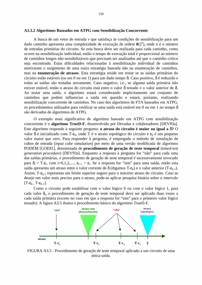
150
A3.3.2 Algoritmos Baseados em ATPG com Sensibilização Concorrente
A busca de um vetor de entrada v que satisfaça às condições de sensibilização para umdado caminho apresenta uma complexidade de execução de ordem 0(2n), onde n é o númerode entradas primárias do circuito. Se esta busca deve ser realizada para cada caminho, comoocorre na sensibilização individual, então o tempo de execução total é proporcional ao númerode caminhos longos não-sensibilizáveis que precisam ser analisados até que o caminho críticoseja encontrado. Estas dificuldades relacionadas à sensibilização individual de caminhosmotivaram o surgimento de uma outra estratégia baseada não na enumeração de caminhos,mas na enumeração de atrasos. Esta estratégia reside em testar se as saídas primárias docircuito estão estáveis (ou em 0 ou em 1) para um dado tempo δ. Caso positivo, δ é reduzido etodas as saídas são testadas novamente. Caso negativo, i.e., se alguma saída primária nãoestiver estável, então o atraso do circuito está entre o valor δ testado e o valor anterior de δ.Ao testar uma saída, o algoritmo estará considerando implicitamente um conjunto decaminhos que podem influenciar a saída em questão e estará, portanto, realizandosensibilização concorrente de caminhos. No caso dos algoritmos de FTA baseados em ATPG,os procedimentos utilizados para verificar se uma saída está estável em 0 ou em 1 no tempo δsão derivados de algoritmos de ATPG.
O exemplo mais significativo de algoritmo baseado em ATPG com sensibilizaçãoconcorrente é o algoritmo TrueD-F, desenvolvido por Devadas e colaboradores [DEV93a].Este algoritmo responde à seguinte pergunta: o atraso do circuito é maior ou igual a δ? Ovalor δ é inicializado com T-ε0, onde T é o atraso topológico do circuito e ε0 é um pequenovalor maior que zero. Para responder à pergunta, é empregado o método de simulação decubos de entrada (input cube simulation) por meio de uma versão modificada de algoritmoPODEM [GOE81], denominada de procedimento de geração de teste temporal (timed-testgeneration procedure) [DEV93a]. Enquanto a resposta à pergunta for “não” para cada umadas saídas primárias, o procedimento de geração de teste temporal é sucessivamente invocadopara δi = T-εi, com i=0,1,2,...., εi+1 > εi. Se a resposta for “sim” para uma saída, então estasaída apresenta um atraso entre o valor corrente de δ (digamos T-εk) e o valor anterior (T-εk-1).Assim, T-εk-1 representa um limite superior seguro para o máximo atraso do circuito. Caso sedeseje um valor mais preciso para o atraso, pode-se aplicar pesquisa binária sobre o intervalo[T-εk , T-εk-1].
Como o circuito pode estabilizar com o valor lógico 0 ou com o valor lógico 1, paracada valor δi, o procedimento de geração de teste temporal deve ser aplicado duas vezes acada saída primária (exceto no caso em que a resposta for “sim” para o primeiro valor lógicotestado). A figura A3.5 ilustra o procedimento básico do algoritmo TrueD-F.
atraso real(desconhecido)
atraso
T-ε1T-ε2T-ε3T-ε4 T
atrasotopológico
“não”“sim”
FIGURA A3.5 - Procedimento de geração de teste temporal aplicado a um circuito de umaúnica saída.

151
A fim de determinar se o atraso máximo (atraso crítico) numa saída primária docircuito é maior ou igual a δi para o valor lógico lvalue, o procedimento de geração de testetenta justificar lvalue na saída considerada com atraso maior ou igual a δi. Isto é feito pormeio de simulação de cubos, de maneira similar à realizada pelo algoritmo PODEM. Como oPODEM permite uma exploração sistemática e exaustiva do espaço das entradas, caso elefalhe em encontrar um cubo de entrada capaz de justificar lvalue na saída do circuito para ovalor de atraso δi considerado, então a resposta à pergunta será “não” (para a saída testada epara o valor lógico lvalue considerado). Em outras palavras, o problema de determinar oatraso do circuito é transformado num problema de geração de teste para uma falha decolagem simples localizada na saída primária do circuito.
A chamada de mais alta hierarquia do procedimento de geração de teste temporal(timed_test) é descrita pelo pseudocódigo que segue (figura A3.6). Tal qual no algoritmoPODEM puramente lógico, há uma lista de justificação jlist armazenando as linhas docircuito que precisam ser justificadas. O procedimento inicia pela inserção de uma dada saídaprimária po em jlist com valor lógico lvalue (0 ou 1) e assumindo delay como sendo olimite inferior do atraso do circuito a ser testado (δi). Então, o procedimento SEARCH_1 échamado.
timed_test(po,delay,lvalue) v.value = lvalue; v.lower = delay; v.upper = INFINITY;
modify_jlist (po,v,jlist); backward schedule po;
status = SEARCH_1(jlist); return(status);
FIGURA A3.6 – Pseudocódigo para a chamada de mais alta hierarquia do procedimento degeração de teste temporal.
As funções de busca são similares àquelas encontradas no algoritmo PODEM e estãodescritas pelos pseudocódigos das figuras A3.7 e A3.8. A função SEARCH_1 chama a funçãoBACKTRACE para, partindo da saída primária po, encontrar uma entrada primária cujo valorlógico ainda é desconhecido. A entrada primária identificada é inicialmente ajustada ao valorlógico 1 e então a função IMPLY é chamada. Esta, por sua vez, leva a cabo uma rodada desimulação de cubos para teste temporal considerando as condições de sensibilização docritério exato do modo flutuante (no PODEM original, que a partir daqui será referido porPODEM lógico, a função IMPLY corresponde à simulação de cubos com três valores lógicos esem informação de atrasos). A função de implicação pode levar a uma situação de conflito, oqual pode ser de duas naturezas distintas: lógica ou temporal. Se não ocorrer conflito,SEARCH_1 será chamada recursivamente. O procedimento termina com sucesso em SEARCH_1se a lista de justificação tornar-se vazia. No caso de ocorrência de conflito em SEARCH_1, oalgoritmo retrocede ao assinalamento de entrada primária mais recente, assinalando-lhe ovalor lógico 0. Então, a função SEARCH_2, mostrada na figura A3.8, é chamada.
O procedimento BACKTRACE falha se suas funções forem incapazes de encontrar umaentrada primária livre de assinalamento ou se o espaço das entradas tiver sido completamenteexplorado sem sucesso em SEARCH_2. Ocorre conflito se não for possível atribuir a uma linhado circuito o valor lógico que lhe é requerido com o período de tempo necessário. Em caso de

152
conflito ou falha, é necessário desfazer todos os assinalamentos originados do assinalamentode entradas que causou o conflito ou falha.
SEARCH_1(jlist)if(length of jlist is zero) return SUCCEED;
if(BACKTRACE(gate,value,delay,&pi,&pi_value)==FALSE)return(FAILED);
if(IMPLY(pi,pi_value,jlist)!=IMPLY_CONFLICT)search_status = SEARCH_1(jlist);if(search_status == FAILED)restore the state of the network;search_status = SEARCH_2(jlist,pi,1-pi_value);
else
restore the state of the network;search_status = SEARCH_2(jlist,pi,1-pi_value);
return(search_status);
FIGURA A3.7 – Pseudocódigo para o primeiro procedimento de busca.
O procedimento de geração de teste temporal assume que cada porta do circuito (etambém cada aresta) possui uma “variável lógico-temporal” formada por três campos: umlimite inferior e um limite superior de atraso da porta (atrasos no contexto do circuito comoum todo) e um valor lógico. Um passo de pré-processamento inicializa os campos de valoreslógicos com o valor 2 (o qual indica que o valor lógico ainda não está determinado) e oslimites inferior e superior de atraso com os mínimos e máximos atrasos topológicoscomputados a partir das entradas primárias. Na fase de geração de teste, ao serem assinaladosvalores lógicos conhecidos às entradas primárias, os limites inferior e superior de atraso vãosendo aproximados durante a simulação para diante, devido à sensibilização ou bloqueio doscaminhos. Os limites inferior e superior são também modificados pela retro-implicação, nomomento em que novos valores são inferidos em algumas portas, como decorrência dosvalores lógicos e respectivos tempos requeridos para as saídas primárias.
SEARCH_2(jlist,pi,pi_value) backtracks = backtracks + 1 ; if(backtracks > BACKTRACK_LIMIT) return(ABORTED);
if(IMPLY(pi,pi_value,jlist)!=IMPLY_CONFLICT) search_status = SEARCH_1(jlist); if(search_status == FAILED) restore the state of the network;
else
search_status = FAILED; restore the state of the network; return(search_status);
FIGURE A3.8 - Pseudocódigo para o segundo procedimento de busca.

153
Outro elemento importante do procedimento de geração de teste temporal é a lista dejustificação. Portas são incluídas a esta lista durante a retro-implicação e retiradas tantodurante implicação para diante quanto durante a retro-implicação. A qualquer tempo, a lista dejustificação contém as portas cujos valores lógicos ou de atraso precisam ser justificados, oque só se concretiza pelo assinalamento de novas entradas primárias. O fato da lista dejustificação ficar vazia significa que a busca foi concluída com sucesso. Então, a resposta paraa questão “o atraso do circuito é maior ou igual a δ (quando o valor lógico lv é assinalado àsaída considerada)?” é “sim”. Por outro lado, caso o espaço de busca tiver sidocompletamente enumerado sem que a lista de justificação tenha sido esvaziada, a buscafalhou: a resposta para a pergunta é “não”. Uma terceira situação seria o caso em que a buscaé abandonada devido ao número excessivo de retrocessos, quando então a pegunta permanecesem resposta.
É importante ressaltar que a variável lógico-temporal é usada para armazenar tanto osvalores reais (lógicos e de atraso) quanto aqueles valores inferidos por meio da retro-implicação. A diferença entre esse dois casos reside no fato de que, no segundo caso a portarelacionada estará na lista de justificação. De fato, todas as portas cujos valores de entradasnão produzem os valores constantes em sua variável lógico-temporal devem estar na lista dejustificação. Por outro lado, qualquer porta cujas entradas produzem os valores constantes emsua variável lógico-temporal não deve estar na lista de justificação. Estas duas assertivasanteriores caracterizam de maneira precisa a lista de justificação.
Tendo apresentado as duas funções de mais alta hierarquia do procedimento, passemos aexaminar a função imply, a qual é chamada dentro das funções search1 e search2. A funçãoimply é detalhada pelo pseudocódigo da figura A3.9. A entrada primária é assinalada com ovalor lógico devido e o efeito deste assinalamento é propagado pelo circuito usando a funçãoforward_set. Esta função, por sua vez, arrola o tratamento do fanout da entrada primária quefoi modificada e então a função forward_imply realiza uma simulação temporal digirida poreventos. forward_imply é seguida de uma retro-implicação (função backward_imply). Estasduas funções são chamadas de maneira iterativa até que os valores no circuito não mudemmais. Geralmente, o assinalamento de um valor lógico particular a uma porta durante aimplicação para diante ou durante a retro-implicação exige a previsão de tratamento diante detodos os seus fanouts e a previsão de tratamento para trás de todos os seus fanins que estão nalista de justificação (forward e backward scheduling).
Os eventuais conflitos são detectados por ambas funções de implicação. Estes conflitospodem ser de natureza lógica (conflitos lógicos) ou de natureza temporal (conflitostemporais).
imply(pi,pi_value,jlist) v = pi.timed_value; v.value = pi_value; status = forward_set(pi,v,jlist);
while(status==IMPLY_NORMAL) status=forward_imply(jlist);
if(status!=IMPLY_CONFLICT)status=backward_imply(jlist);
return status;
FIGURA A3.9 – Pseudocódigo para o procedimento de implicação.

154
A chave para determinar se é possível ou não justificar um valor lógico numa saída docircuito para um dado tempo reside na adoção de um cálculo temporal de três valores que levaem consideração as condições de sensibilização do critério exato do modo flutuante.Considere uma porta E de duas entradas com atraso d. Cada uma das entradas desta porta ii
pode apresentar um valor lógico pertencente ao conjunto 0,1,2 com limites inferior esuperior de atraso dados por li e ui, respectivamente. O termo “atraso do sinal” será utilizado,ao invés de “tempo de estabilização” [CHE93], pois mesmo portas que apresentam valorlógico não assinalado (i.e., 2) em suas saídas, apresentam valores coerentes para os limitesinferior e superior do atraso. Os resultados para uma simulação de cubos usando o cálculotemporal para uma porta E de duas entradas e para uma porta OU de duas entradas sãomostrados nas tabelas A3.2 e A3.3. Nestas tabelas, lv é o valor lógico na saída da porta,enquanto lo e uo representam os limites inferior e superior do atraso na saída da porta,respectivamente.
TABELA A3.2 – Cálculo temporal de três valores para uma porta E de duas entradas.
i2
i10 1 2
0lvlouo
0min(l1,l2)+d
min(u1,u2)+d
0l2+du2+d
0min(l1,l2)+d
u2+d
1lvlouo
0l1+du1+d
1max(l1,l2)+d
max(u1,u2)+d
2l1+d
max(u1,u2)+d
2lvlouo
0min(l1,l2)+d
u1+d
2l2+d
max(u1,u2)+d
2min(l1,l2)+d
max(u1,u2)+d
TABELA A3.3 - Cálculo temporal de três valores para uma porta OU de duas entradas.
i2
i10 1 2
0lvlouo
0max(l1,l2)+d
max(u1,u2)+d
1l1+du1+d
2l1+d
max(u1,u2)+d
1lvlouo
1l2+du2+d
1min(l1,l2)+d
min(u1,u2)+d
1min(l1,l2)+d
u2+d
2lvlouo
2l2+d
max(u1,u2)+d
1min(l1,l2)+d
u1+d
2min(l1,l2)+d
max(u1,u2)+d
O fato dos algoritmos de FTA baseados em ATPG (com sensibilização concorrente)serem derivados dos próprios algoritmos de ATPG os torna bastante interessantes, pois que asinúmeras técnicas de aceleração já desenvolvidas para os últimos podem ser aplicadas quaseque diretamente aos primeiros.

155
A3.3.1 Algoritmos Baseados em SAT com Sensibilização Concorrente
Conforme discutido nas duas subseções anteriores, nos algoritmos baseados em ATPG,a sensibilização é considerada ou de forma explícita, traçando e testando a sensibilização doscaminhos um a um, ou de forma implícita, justificando valores lógicos nas saídas do circuitopara um dado valor limite de atraso T. Estes procedimentos baseiam-se no algoritmo D e noalgoritmo PODEM, respectivamente.
Nos algoritmos baseados em SAT, entretanto, a sensibilização é testada de formaimplícita, usando solvabilidade Booleana (SAT). Trata-se de uma solução mais ampla, já queo teste de sensibilização (e também a detecção de falhas de colagem) pode ser formuladacomo um problema de solvabilidade.
No contexto dos algoritmos de FTA baseados em SAT, o método proposto por McGeeret al. [MCG93], chamado método exato, merece destaque em função de sua ampla aceitaçãojunto à comunidade de análise de timing. Este método utiliza uma extensão do modelo deatraso não-limitado denominado XBD0 (Extended Bounded Delay-0), no qual um terceirovalor é acrescido ao conjunto de valores Booleanos 0,1. Este terceiro valor, normalmentesimbolizado por 2, é utilizado para modelar o estado indeterminado e também o estadodesconhecido. O método também utiliza um formalismo denominado álgebra de formas deonda, introduzido por Augustin em [AUG89]. O modelo algébrico baseado em formas deonda seria equivalente à álgebra de chaveamento com os operadores Booleanos, tomada nodomínio estático. Dentro desta nova plataforma, o modelo de computação de atraso de porta éredefinido, com o intuito de unir funcionalidade lógica e atraso de porta. Assim, pela novadefinição de atraso de porta, uma porta é vista como um operador que toma as formas de ondaaplicadas às suas entradas e encontra a forma de onda da saída.
Tal como os algoritmos baseados em ATPG com sensibilização concorrente, o métodoexato também baseia-se em enumeração de atrasos, ao invés de enumeração de caminhos.Para enumerar atrasos, o método exato se utiliza de um procedimento análogo àquelediscutido na seção anterior, apenas mudando o método utilizado para testar se todas as saídasprimárias estão estabilizadas para o tempo δ testado. Para este teste, o procedimentoempregado caracteriza recursivamente o conjunto de todos os vetores de entrada capazes defazer com que uma determinada saída primária estabilize com um valor lógico (0 ou 1), para oque é utilizada uma álgebra ternária e o cálculo de forma de onda (waveform calculus).
A álgebra ternária é formada pela adição de um terceiro valor ao conjunto de valores daálgebra Booleana, denotado por 2, e tem o intuito de representar os seguintes fenômenos:
• estado indeterminado, que ocorre enquanto a saída de uma porta está transicionandode 0 para 1 ou vice-versa. Em outras palavras, modela o comportamente analógicode um sinal;
• estado desconhecido, quando não é possível determinar o valor lógico de um sinal,apesar de se saber que o mesmo vale 0 ou 1. Assim, o valor 2 também serve paramodelar a incertitude de cada variável que determina o atraso dos componentes docircuito, tais como variação do processo de fabricação, crosstalk, inclinação darampa do sinal de entrada etc.
Sumarizando, o valor 2 representa os casos em que o valor na saída de uma porta nãopode ser assegurado como sendo um valor Booleano.
Dado um tempo δ em que se deseja testar a estabilização de uma saída, o método exatoencontra a função característica de cada nó. Por meio da função característica, é possível

156
determinar se as condições (Booleanas e temporais) necessárias para que o nó estejaestabilizado no tempo desejado podem ser satisfeitas ou não, o que é feito utilizandosolvabilidade Booleana. Assim, o método exato determina, de maneira recursiva, as equaçõescaracterísticas dos nós do circuito que podem influenciar a saída que se deseja testar. Após, éaplicada solvabilidade Booleana ao conjunto de funções características. Se for possívelresolver o sistema de função características, então a saída está estável no tempo δ. Por outrolado, caso não seja possível encontrar uma solução, então a saída não está estável e seu atrasoé maior do que δ. É importante ressaltar que, dado um tempo δ, este procedimento deve serrealizado para cada saída. Além disso, para cada novo valor de δ será necessário testar-se cadauma das saídas. Ora, sabendo-se que os métodos de testes de solvabilidade exigem grandeesforço computacional, conclui-se que a complexidade (em termos de tempo) dos algoritmosde FTA baseados em SAT é proporcional ao passo de tempo utilizado. Além disso, conformemencionado em [MCG93], em circuitos muito grandes e/ou em circuitos que apresentam umgrande número de caminhos com atrasos distintos, o número de funções característicasnecessárias torna-se muito grande, aumentando ainda mais o tempo de execução. Em funçãodisso, foram propostas algumas regras de poda no procedimento de geração das funçõescaracterísticas que, no entanto, conseguem minorar o problema apenas de forma parcial. Emfunção desta dificuldade, os algoritmos baseados em SAT com sensibilização concorrente temse mostrado de aplicação restrita quando modelos físicos de atraso mais realistas sãoutilizados. Isto porque, da adoção de tais modelos resulta uma individualização dos caminhos,no sentido de que poucos caminhos compartilham um mesmo valor de atraso.
A formulação teórica do método exato está descrita em maiores detalhes nas subseções5.4.2 e 5.4.3 desta tese.
A próxima seção apresenta um algoritmo de FTA baseado em ATPG, comsensibilização concorrente, capaz de operar sobre circuitos que contenham portas complexas.
A3.4 Análise de Timing Funcional de Circuitos Contendo PortasComplexas
As primeiras técnicas de FTA realizavam sensibilização individual de caminhosutilizando variações do algoritmo D e critérios de sensibilização simplificados, buscandoreduzir o tempo execução. Entretanto, logo a sensibilização individual se mostrouimpraticável mesmo para circuitos de complexidade moderada, e a sensibilização concorrentetomou-lhe o lugar. Com a sensibilização concorrente as técnicas de FTA passaram a utilizaruma abordagem baseada em “enumeração de atraso”, ao invés de uma abordagem baseada em“enumeração de caminhos”. Além de não necessitar da fase de enumeração, a sensibilizaçãoconcorrente também permite a adoção do critério de sensibilização exato do modo flutuante, oqual é o único capaz de fornecer o atraso exato sob o modo flutuante.
Entretanto, toda a teoria que embasa os métodos de teste de sensibilização de caminhose também os próprios critérios de sensibilização foram desenvolvidos assumindo circuitoscompostos por portas simples, isto é, portas E/NÃO-E, OU/NÃO-OU e inversores.Conseqüentemente, se um circuito combinacional que contenha portas mais complexas deveser analisado, a ferramenta de FTA a ser utilizada deve estar apta não somente a reconhecertais portas mas também de tratar coerentemente o circuito de acordo com o modelocomputacional de atraso adotado. Isto pode ser realizado ou pela inclusão de uma fase de pré-processamento ou pela extensão do algoritmo/método de computação do atraso do circuito edas condições de sensibilização do critério adotado.

157
A disponibilização de geradores de macrocélulas CMOS eficientes tais como osapresentados em [CAD99] e [MOR97], e de ferramentas de mapeamento tecnológicoindependentes de bibliotecas [REI97] tornou possível o uso extensivo de portas complexas(sobretudo portas CMOS estáticas) no projeto físico de grandes blocos combinacionais. Destemodo, a capacidade de tratar circuitos que contenham portas complexas passa a ser altamentedesejável para novas ferramentas de FTA.
Antes de iniciar uma discussão sobre a análise de timing funcional de circuitos quecontenham portas complexas, é importante prover definições para portas simples e portascomplexas. No contexto desta tese, uma porta simples corresponde a uma implementaçãofísica de um operador básico da álgebra Booleana. Assim, são portas simples as portas E, OU,NÃO-E, NÃO-OU (com qualquer número de entradas) e o inversor. Particularmente, portassimples CMOS são portas simples que podem ser implementadas diretamente em tecnologiaCMOS, ou seja, portas NÃO-E, NÃO-OU e inversor. Uma porta complexa corresponde a umaimplementação física de qualquer função Booleana de complexidade maior do que osoperadores Booleanos básicos. Especificamente, uma porta complexa CMOS estática (StaticCMOS Complex Gate - SCCG) corresponde a uma porta complexa implementada emtecnologia CMOS.
Inicialmente, será investigado o caso particular das SCCGs, em função de suaimportância. Após, serão feitas considerações sobre a extensão dos modelos e algoritmospropostos para o caso de portas complexas quaisquer.
Uma porta CMOS estática é implementada por uma rede de transistores CMOSconectados segundo uma topologia de “restauração completa”, composta por uma rede PMOSe uma rede NMOS. A rede PMOS é capaz de prover um caminho entre a saída da porta e amassa (Vdd), enquanto que a rede NMOS é capaz de prover um caminho entre a saída daporta e a terra (Gnd). As redes NMOS e PMOS possuem mesmo número de transistores. Poruma questão de simplicidade, iremos assumir que uma SCCG é uma porta CMOS estática naqual ambas redes de transistores apresentam apenas associações série/paralelo, e sendo redePMOS o dual da rede NMOS, em termos de associação de transistores. A figura A3.10 mostraum exemplo de SCCG. Note-se que, para uma porta CMOS estática de n entradas, há n paresNMOS/PMOS conectados pela grade, formando cada par uma entrada da porta.
(b)
S
GND
VDD
A
A
B
B
C
C
D
D
E
E
A
CS
B
D
E
(a)
(b)
S
GND
VDD
A
A
B
B
C
C
D
D
E
E
(b)
S
GND
VDD
A
A
B
B
C
C
D
D
E
E
S
GND
VDD
A
A
B
B
C
C
D
D
E
E
A
CS
B
D
E
(a)
A
CS
B
D
E
A
CCS
BB
DD
EE
(a)
FIGURA A3.10 - Exemplo de SCCG.
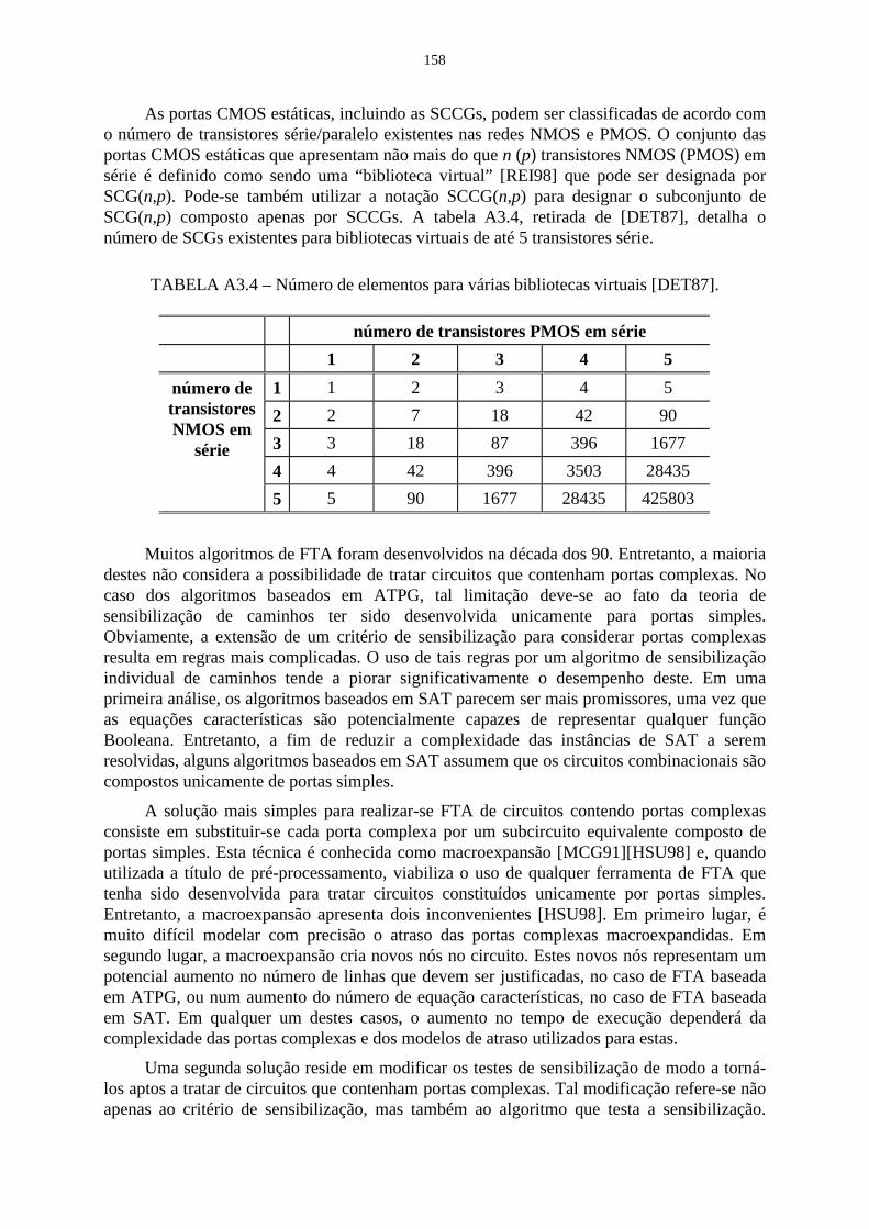
158
As portas CMOS estáticas, incluindo as SCCGs, podem ser classificadas de acordo como número de transistores série/paralelo existentes nas redes NMOS e PMOS. O conjunto dasportas CMOS estáticas que apresentam não mais do que n (p) transistores NMOS (PMOS) emsérie é definido como sendo uma “biblioteca virtual” [REI98] que pode ser designada porSCG(n,p). Pode-se também utilizar a notação SCCG(n,p) para designar o subconjunto deSCG(n,p) composto apenas por SCCGs. A tabela A3.4, retirada de [DET87], detalha onúmero de SCGs existentes para bibliotecas virtuais de até 5 transistores série.
TABELA A3.4 – Número de elementos para várias bibliotecas virtuais [DET87].
número de transistores PMOS em série
1 2 3 4 5
1 1 2 3 4 5
2 2 7 18 42 90
3 3 18 87 396 1677
4 4 42 396 3503 28435
número detransistoresNMOS em
série
5 5 90 1677 28435 425803
Muitos algoritmos de FTA foram desenvolvidos na década dos 90. Entretanto, a maioriadestes não considera a possibilidade de tratar circuitos que contenham portas complexas. Nocaso dos algoritmos baseados em ATPG, tal limitação deve-se ao fato da teoria desensibilização de caminhos ter sido desenvolvida unicamente para portas simples.Obviamente, a extensão de um critério de sensibilização para considerar portas complexasresulta em regras mais complicadas. O uso de tais regras por um algoritmo de sensibilizaçãoindividual de caminhos tende a piorar significativamente o desempenho deste. Em umaprimeira análise, os algoritmos baseados em SAT parecem ser mais promissores, uma vez queas equações características são potencialmente capazes de representar qualquer funçãoBooleana. Entretanto, a fim de reduzir a complexidade das instâncias de SAT a seremresolvidas, alguns algoritmos baseados em SAT assumem que os circuitos combinacionais sãocompostos unicamente de portas simples.
A solução mais simples para realizar-se FTA de circuitos contendo portas complexasconsiste em substituir-se cada porta complexa por um subcircuito equivalente composto deportas simples. Esta técnica é conhecida como macroexpansão [MCG91][HSU98] e, quandoutilizada a título de pré-processamento, viabiliza o uso de qualquer ferramenta de FTA quetenha sido desenvolvida para tratar circuitos constituídos unicamente por portas simples.Entretanto, a macroexpansão apresenta dois inconvenientes [HSU98]. Em primeiro lugar, émuito difícil modelar com precisão o atraso das portas complexas macroexpandidas. Emsegundo lugar, a macroexpansão cria novos nós no circuito. Estes novos nós representam umpotencial aumento no número de linhas que devem ser justificadas, no caso de FTA baseadaem ATPG, ou num aumento do número de equação características, no caso de FTA baseadaem SAT. Em qualquer um destes casos, o aumento no tempo de execução dependerá dacomplexidade das portas complexas e dos modelos de atraso utilizados para estas.
Uma segunda solução reside em modificar os testes de sensibilização de modo a torná-los aptos a tratar de circuitos que contenham portas complexas. Tal modificação refere-se nãoapenas ao critério de sensibilização, mas também ao algoritmo que testa a sensibilização.

159
Desde que há mais de um algoritmo para testar a sensibilização de caminhos, esta soluçãopode ser desdobrada em várias soluções.
Em [HSU98], por exemplo, é apresentado um algoritmo de FTA capaz de operardiretamente sobre circuitos com portas complexas. Com o intuito de evitar a macroexpansão,as condições para sensibilização exata no modo flutuante são estendidas, de modo aconsiderar portas complexas. Estas condições de sensibilização estendidas são utilizadas porum algoritmo baseado em sensibilização individual derivado do algoritmo D. Os resultadosmostrados em [HSU98] permitem comparar modelos de atraso para macroexpansão, bemcomo comparar o uso da macroexpansão com o algoritmo que testa diretamente portascomplexas. Por outro lado, todos os resultados foram obtidos pelo uso de algoritmos baseadosem sensibilização individual de caminhos, a qual, sabidamente, não representa o estado-da-arte por sofrer de um problema conhecido por “explosão de caminhos”.
Conforme já apresentado no item A3.3, o procedimento de geração de teste temporal deDevadas et al. [DEV93a] é um algoritmo de sensibilização concorrente de caminhos baseadoem ATPG derivado do algoritmo PODEM [GOE81]. No procedimento de geração de testetemporal, o problema de se calcular o atraso de um circuito é transformado num conjunto degeração de testes para falhas de colagem “temporais” imaginadas como ocorrendo nas saídasprimárias do circuito. O procedimento tem então o objetivo de justificar tais falhas decolagem.
A fim de se poder estender o procedimento de geração de teste temporal para circuitosque contenham portas complexas, é necessário generalizar o cálculo temporal para portasE/OU de n entradas. Para tanto, lança-se mão dos conceitos de valor controlante e valor não-controlante, conforme definidos no escopo de teste. Assim, dada uma porta g tipo E/OU de nentradas, podemos classificar seu estado lógico conforme os seguintes casos:
1. Casos em que ao menos uma das entradas de g apresenta o valor controlante (c(g)).As demais entradas podem apresentar ou o valor não-controlante (nc(g)) ou o valor2;
2. Caso em que todas as entradas de g apresentam o valor não-controlante (nc(g));3. Casos em que ao menos uma das entradas de g apresenta o valor 2, mas nenhuma
entrada apresenta o valor controlante (c(g)). As demais entradas podem apresentar ovalor não-controlante (nc(g)).
A partir da identificação dos casos possíveis, chega-se à generalização das regrasoriginalmente expressas nas tabelas A3.2 e A3.3. Também é possível expandir tais regras demodo a se considerar a polaridade de saída das portas, o que permite tratar portas NÃO-E eNÃO-OU. As regras generalizadas são mostradas na tabela A3.5.
TABELA A3.5 – Regras generalizadas para o cálculo temporal de três valores para portassimples de n entradas.
grupo regras lv
1louo
min li | i= c(g) or i=2 + dmin uj | j= c(g) + d
pol(g) ⊕ c(g)
2louo
max li + dmax uj + d
pol(g) ⊕ nc(g)
3louo
min li | i=2 + dmax uj + d
2

160
As regras resumidas na tabela A3.5 podem ainda ser representadas de maneira gráfica,conforme mostram as figuras A3.11, A3.12 e A3.13. Por uma questão de simplicidade, tantona tabela A3.5 como nas figuras A3.11, A3.12 e A3.13 assumiu-se um atraso único por porta.Modelos computacionais de atraso mais sofisticados serão discutidos mais adiante.
i1
i2
i3
og
i4
l1 u1c(g)
2l2 u2
l3 u3c(g)
u4l4nc(g)
min li | i= c(g) or i=2 + d
min uj | j= c(g) + d
pol(g) ⊕ c(g)
l2 + d u1 + d
d= gate delay
i1
i2
i3
og
i4
i1
i2
i3
og
i4
l1 u1c(g)
2l2 u2
l3 u3c(g)
u4l4nc(g)
l1 u1c(g)
l1 u1c(g)c(g)
2l2 u2
2l2 u2
l3 u3c(g)
l3 u3c(g)c(g)
u4l4nc(g)
u4l4nc(g)nc(g)
min li | i= c(g) or i=2 + d
min uj | j= c(g) + d
pol(g) ⊕ c(g)
l2 + d u1 + d
d= gate delay
FIGURA A3.11 – Cálculo temporal de três valores para o grupo 1.
l1 + d u3 + d
max li + d max uj + d
pol(g) ⊕ nc(g)
l1 u1nc(g)
nc(g)l2 u2
l3 u3nc(g)
u4l4nc(g)
i1
i2
i3
og
i4
d= gate delay
l1 + d u3 + d
max li + d max uj + d
pol(g) ⊕ nc(g)
l1 u1nc(g)
nc(g)l2 u2
l3 u3nc(g)
u4l4nc(g)
l1 u1nc(g)
l1 u1nc(g)nc(g)
nc(g)l2 u2
nc(g)l2 u2
l3 u3nc(g)
l3 u3nc(g)nc(g)
u4l4nc(g)
u4l4nc(g)nc(g)
i1
i2
i3
og
i4
i1
i2
i3
og
i4
d= gate delay
FIGURA A3.12 - Cálculo temporal de três valores para o grupo 2.
l2 + d u3 + d
min li | i=2 + d max uj + d
l1 u1nc(g)
2 l2 u2
l3 u32
u4l4nc(g)
i1
i2
i3
og
i4
2
d= gate delay
l2 + d u3 + d
min li | i=2 + d max uj + d
l1 u1nc(g)
2 l2 u2
l3 u32
u4l4nc(g)
l1 u1nc(g)
l1 u1nc(g)nc(g)
2 l2 u2
2 l2 u2
l3 u32
l3 u322
u4l4nc(g)
u4l4nc(g)nc(g)
i1
i2
i3
og
i4
i1
i2
i3
og
i4
2
d= gate delay
FIGURA A3.13 - Cálculo temporal de três valores para o grupo 3.
Assumindo-se que a função lógica de uma porta qualquer g esteja na forma fatorada eutilizando-se uma estrutura de dados apropriada para representá-la, a aplicação das regrasgeneralizadas é direta. Considere, por exemplo, a SCCG mostrada na figura A3.14a. A função

161
lógica desta porta é dada por S = A ⋅((B ⋅C) +(D ⋅E)) e pode ser representada por uma “árvoreda função” (figura A3.14c). Examinando-se esta árvore da função nota-se que, dado umassinalamento de valores temporais de entrada (valores lógicos e respectivos limites inferior esuperior de atraso), os valores temporais na saída podem ser obtidos mediante a aplicaçãosucessiva das regras da tabela A3.5 para cada subárvore, iniciando-se pela subárvore maispróxima da base, desde que sejam feitas as seguintes assertivas:
1. Todas as subárvores, exceto a raiz, apresentam atraso de propagação zero epolaridade igual a zero
2. atraso de propagação da porta é aplicado somente sobre os limites inferior e superiorde atraso da saída da porta, i.e., sobre os valores temporais resultantes da avaliaçãoda subárvore de maior hierarquia.
3. A polaridade da porta é tratada somente quando a subárvore de maior hierarquia éprocessada.
A primeira e a segunda assertiva permitem que se divida a avaliação temporal da SCCGem dois passos independentes. No primeiro passo, o valor lógico da saída e os limites inferiore superior de atraso são computados para um atraso de propagação da porta igual a zero.Chamaremos este intervalo de atrasos de “limites de atraso de primeira ordem”. Num segundopasso, os limites inferior e superior reais são computados por meio da adição do atraso depropagação da porta aos limites de atraso de primeira ordem. Este segundo passo leva emconta o modelo computacional de atraso adotado para as portas.
(b)
S
GND
VDD
A
A
B
B
C
C
D
D
E
E
A
CS
B
D
E
(a)
+
. .
A
D EB C
.
(c)
(b)
S
GND
VDD
A
A
B
B
C
C
D
D
E
E
(b)
S
GND
VDD
A
A
B
B
C
C
D
D
E
E
S
GND
VDD
A
A
B
B
C
C
D
D
E
E
A
CS
B
D
E
(a)
+
. .
A
D EB C
.
(c)
A
CS
B
D
E
(a)
A
CS
B
D
E
A
CCS
BB
DD
EE
(a)
+
. .
A
D EB C
.
(c)
+
. .
A
D EB C
.
+
. .
A
D EB C
.
(c)
FIGURA A3.14 - Exemplo de SCCG: símbolo para o nível lógico (a), esquemático detransistores (b) árvore da função (c).
A figura A3.15 ilustra a aplicação das regras do cálculo temporal aplicadas à SCCG dafigura A3.14.

162
A
C
B
D
E
S
S0
S1
S2
A S2
.S
+A
S0 S1
.
nodosintermediários
+
. .
D EB C
.
A
FIGURA A3.15 – Uso do cálculo temporal de três valores para avaliar uma SCCG.
Uma vez proposto um procedimento para determinar os limites de atraso de primeiraordem na saída de uma porta complexa, faz-se necessário investigar modelos computacionaisde atraso para portas que sejam válidos para o cálculo do atraso flutuante de um circuito. Afim de revelar a relação que existe entre o modelo computacional de atraso de circuitos e omodelo computacional de atraso de portas (e também, o modelo físico de atraso),consideremos a porta NÃO-E de 3 entradas mostrada na figura A3.16. Considere também queo vetor v=(a=1;b=1;c=0) seja aplicado a suas entradas. A fim de se determinar o atrasoflutuante desta porta NÃO-E sob o vetor v, é necessário examinar todas as combinações deentrada contidas em tal vetor, encontrando o pior atraso. Para iniciar, é necessário lembrar queno modo flutuante, um valor 0 representa tanto a transição de descida quanto o valor 0estático, enquanto que um valor 1 representa tanto a transição de subida quanto o valor 1estático. Então, substituindo-se 0 por ↓ ou por 0 e substituindo-se 1 por ↑ ou por 1, obtém-seum total de 8 possibilidades de pares de vetores (figura A3.16b) o que permite estabelece-seuma relação entre o modo flutuante e o modo de transição, no que se refere ao modelo deatraso de portas lógicas.
um vetor flutuante
110
1
(a)
pares de vetores associados
1 or ↑110
↑10
1↑0
↑↑0
11↓
↑↑↓
↑1↓
1↑↓
or oror oror or or
(b)
FIGURA A3.16 – Relação entre modo flutuante e modo de transição: um vetor flutuanteaplicado a uma porta NÃO-E de 3 entradas (a) e os 8 pares de vetores associados (b).

163
Antes de continuar a discussão, é conveniente definir-se vetor flutuante e atrasoflutuante.
Definição A3.1: vetor flutuante e atraso flutuante
Um vetor flutuante é um assinalamento de valores lógicos aplicado às entradas de umaporta ou às entradas do circuito, quando assume-se que o circuito está operando nomodo flutuante. O atraso computado para a porta (para o circuito) assumindo-se talmodo de operação é chamado atraso flutuante da porta (do circuito).
Dada a definição para vetor flutuante, vale lembrar que um vetor flutuante de n variáveiscontém 2n pares de vetores, dentre os quais um é composto por dois vetores iguais. A tabelaA3.6 mostra todos os vetores flutuantes possíveis e os pares de vetores associados para umaporta NÃO-E de 3 entradas. Os pares hachureados em cinza claro são responsáveis por umaúnica transição de saída, enquanto que os pares hachureados em cinza escuro podem provocaruma transição espúria (glicth) na saída da porta.
TABELA A3.6 – Relação entre vetores do modo flutuante e vetores do modo de transição.
vetor de entrada 000 001 010 011 100 101 110 111
000 001 010 011 100 101 110 111
↓00 ↓01 ↓10 ↓11 ↑00 ↑01 ↑10 ↑11
0↓0 0↓1 0↑0 0↑1 1↓0 1↓1 1↑0 1↑1
00↓ 00↑ 01↓ 01↑ 10↓ 10↑ 11↓ 11↑
↓↓ 0 ↓↓ 1 ↓↑ 0 ↓↑ 1 ↑↓ 0 ↑↓ 1 ↑↑ 0 ↑↑ 1
↓0↓ ↓ 0↑ ↓1↓ ↓1↑ ↑ 0↓ ↑ 0↑ ↑1↓ ↑1↑
0↓↓ 0↓↑ 0↑↓ 0↑↑ 1↓↓ 1↓↑ 1↑↓ 1↑↑
pares de vetores
associados
↓↓↓ ↓↓↑ ↓↑↓ ↓↑↑ ↑↓↓ ↑↓↑ ↑↑↓ ↑↑↑
valor lógico da saída 1 1 1 1 1 1 1 0
Indo um pouco além, é possível criar-se uma tabela de equivalência entre modoflutuante e modo de transição como a tabela A3.6 para cada uma das 256 funções Booleanasde 3 variáveis. Desde que a associação entre vetores flutuantes e pares de vetores é fixa, asfunções lógicas de 3 entradas se distinguiriam pelos valores lógicos resultantes na saída etambém pelos pares de vetores que influenciam a computação do atraso da porta.Potencialmente, pode-se construir tabelas de equivalência para qualquer função lógica de nentradas.
Uma contribuição da tabela de equivalência reside no fato de que ela permite aidentificação dos modelos computacionais de atraso para portas a serem usados para calcularo atraso flutuante de um circuito. Mais especificamente, a tabela diz que uma porta podeapresentar ao menos um atraso distinto por vetor flutuante de entrada. De maneira maisconservadora, pode-se considerar que o modelo computacional de atraso de porta maisdetalhado para o modo flutuante corresponde a assumir-se um valor de atraso por vetorflutuante. Tal modelo será referenciado por modelo de atraso de vetor.

164
Um modelo menos preciso, porém ainda correto do ponto de vista da análise de timing,corresponde a agrupar os vetores flutuantes de entrada de acordo com o tipo de transição desaída da porta. Assim, a cada porta é assinalado um atraso de descida, correspondendo aomáximo atraso dentre os vetores flutuantes que provocam uma transição de descida, e umatraso de subida, correspondendo ao máximo atraso dentre os vetores flutuantes queprovocam uma transição de subida. Tal modelo será chamado modelo de atraso desubida/descida.
Um terceiro modelo corresponde a assinalar um único valor de atraso por porta,chamado de modelo de atraso único. Naturalmente, este é o modelo menos preciso, emboraainda correto.
É importante ressaltar que, para obter-se um cálculo robusto de atraso flutuante docircuito, os valores de atraso de portas a serem usados em cada um dos três modelos devecorresponder ao limite superior para o atraso da porta, considerando-se todas as instâncias docircuito fabricado. Isto significa que o modelo físico de atraso usado ou o método deestimativa de atraso deve ser capaz de fornecer o valor correspondente ao pior casoindividualmente para cada componente.
Uma análise mais cuidadosa da tabela A3.6 permite ainda concluir que o formato deatraso pino-a-pino, normalmente utilizado na caracterização de standard-cells, não éapropriado para a computação do atraso flutuante desde que considera somente parte de todosos vetores flutuantes de entrada. Por exemplo, no caso de uma porta de 3 entradas, o formatopino-a-pino cobre apenas seis pares de vetores: ↓11, 1↓1, 11↓ , ↑11, 1↑1, 11↑ . Ou seja,apenas as situações em que ocorre uma única transição de entrada.
Uma segunda contribuição da tabela de equivalência entre modo flutuante e modo detransição é a própria associação entre um dado vetor flutuante e os pares de vetores subscritos.Tal informação é útil quando se deseja caracterizar o atraso de uma porta, sobretudo se ométodo de caraterização for simulação elétrica. Neste caso, apenas os pares de vetores quepodem produzir uma transição de saída devem ser simulados, o que pode reduzirsignificativamente o número de casos. Por outro lado, no caso de caracterização por meio deformulação analítica, a informação da tabela de equivalência pode ser usada para ajustar ouadaptar o conjunto de equações de modo a cobrir apenas os pares de vetores de interesse.
Tendo derivado regras seguras para determinar o atraso das portas sob qualquer um dostrês modelos computacionais de atraso de porta, faz-se necessário considerar a aplicação detais regras no cálculo dos limites inferior e superior de atraso de uma porta usando oprocedimento de implicação para diante. Retomando as regras do cálculo temporal de trêsvalores descritas na tabela A3.5, as situações possíveis de vetores flutuantes podem serclassificadas nos três grupos que seguem:
1. Casos em que ao menos uma das entradas de g apresenta o valor controlante (c(g)).As demais entradas podem apresentar ou o valor não-controlante (nc(g)) ou o valor2;
2. Caso em que todas as entradas de g apresentam o valor não-controlante (nc(g));3. Casos em que ao menos uma das entradas de g apresenta o valor 2, mas nenhuma
entrada apresenta o valor controlante (c(g)). As demais entradas podem apresentar ovalor não-controlante (nc(g)).
Os grupos 1 e 3 referem-se aos casos onde uma das entradas da porta apresenta o valor2. No contexto do cálculo de três valores, um 2 representa a existência ou do valor lógico 0 oudo valor lógico 1. Em decorrência disto, podemos introduzir a definição de cubo flutuante:

165
Definição A3.2: cubo flutuante
Dado o cálculo de três valores, um cubo flutuante é um assinalamento de valoreslógicos tal que ao menos um destes corresponde ao valor 2. O número de vetoresflutuantes contidos em um cubo flutuante é igual a 2m, onde m é o número de posiçõesque apresentam o valor 2.
Com efeito, um cubo flutuante contém ao menos dois vetores flutuantes e desta forma,pode ser visto como uma variação do modelo de atraso de subida/descida. A fim de se garantirmáxima precisão, é necessário considerar o máximo e o mínimo atrasos da porta sob um dadocubo. A partir de tal assertiva, o atraso de uma porta sob um cubo terá uma forma invariante,independentemente do modelo computacional de atraso de porta. Para efeitos ilustrativos,considere a aplicação do cubo flutuante 022 à SCCG da figura A3.17, a qual implementa a
função lógica CBAS ⋅+= . A tabela A3.7 mostra a equivalência entre o modo flutuante e omodo de transição para tal porta. Note que a saída desta SCCG será 1 quando o vetor flutuanteaplicado a suas entradas pertencer a 000, 001, 010 e será 0 quando o vetor flutuanteaplicado a suas entradas pertencer a 011, 100, 101, 110, 111. Se o procedimento de cálculodo atraso assumir o modelo de atraso de vetor, então o atraso desta SCCG para o cubo 022terá máximo e mínimo limites de atraso dados por maxd(000),d(001),d(010),d(011) emind(000),d(001),d(010),d(011), respectivamente, onde d(000), d(001), d(010) e d(011) sãoos atrasos para os vetores flutuantes 000, 001, 010 e 011. Por outro lado, se o procedimento decálculo do atraso assumir o modelo de atraso de subida/descida, então o máximo e o mínimolimites de atraso serão dados por maxtpLHmax , tpHLmax e mintpLHmin , tpHLmin. Entretanto,para esta SCCG, tpLHmax=maxd(000),d(001),d(010) e tpLHmin=mind(000),d(001),d(010),enquanto que tpHLmax=tpHLmin=d(011), resultando nos mesmos valores de máximo e mínimoatrasos fornecidos pelo modelo de atraso de vetor. De forma análoga, pode-se declarar que oatraso flutuante deste cubo para o modelo de atraso subida/descida irá resultar nos mesmosvalores de máximo e mínimo atrasos calculados pelos outros dois modelos de atraso de porta.
pares de vetores associados
um vetor flutuante
022
2
0 or 1000
001
010
011
or or or
(a)
(b)
FIGURA A3.17 – Atraso da SCCG da figura A3.17 para o cubo flutuante 022.
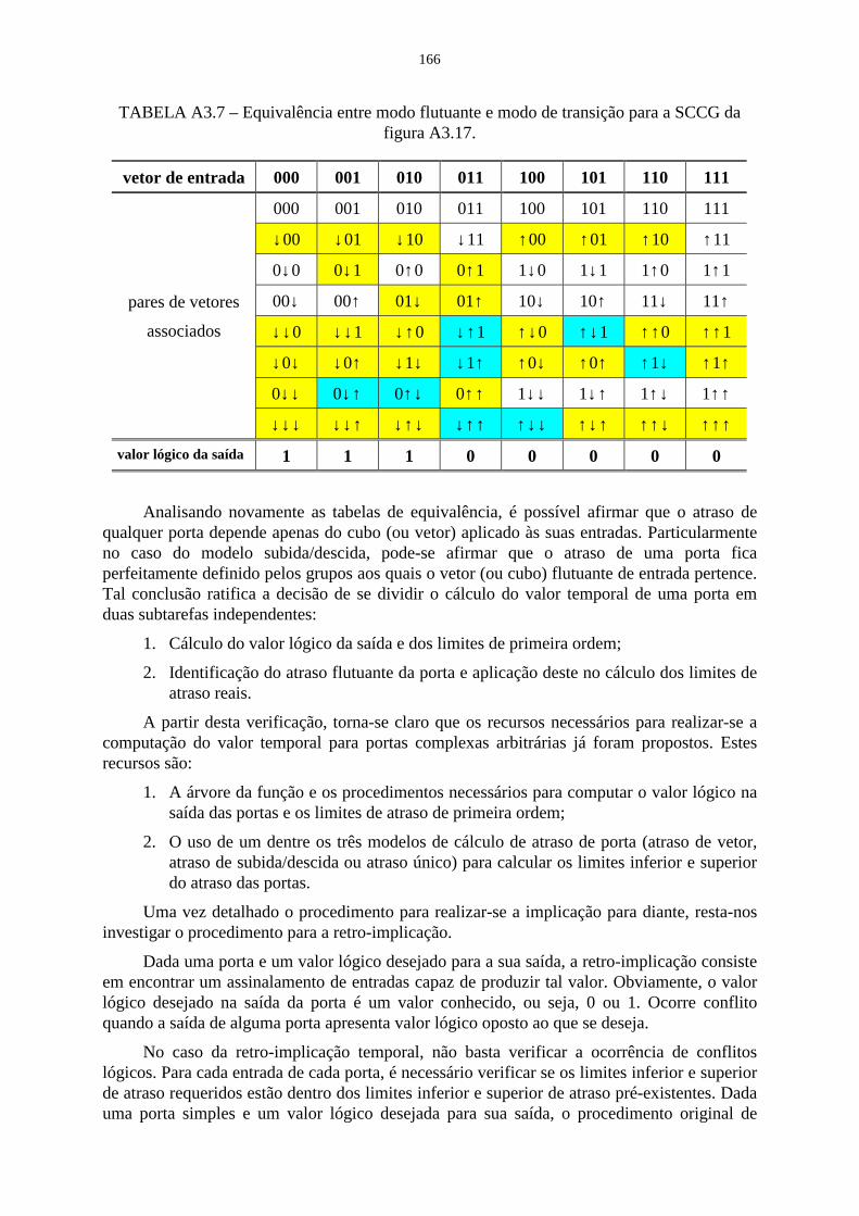
166
TABELA A3.7 – Equivalência entre modo flutuante e modo de transição para a SCCG dafigura A3.17.
vetor de entrada 000 001 010 011 100 101 110 111
000 001 010 011 100 101 110 111
↓00 ↓01 ↓10 ↓11 ↑00 ↑01 ↑10 ↑11
0↓0 0↓1 0↑0 0↑1 1↓0 1↓1 1↑0 1↑1
00↓ 00↑ 01↓ 01↑ 10↓ 10↑ 11↓ 11↑
↓↓ 0 ↓↓ 1 ↓↑ 0 ↓↑ 1 ↑↓ 0 ↑↓ 1 ↑↑ 0 ↑↑ 1
↓0↓ ↓0↑ ↓1↓ ↓1↑ ↑0↓ ↑0↑ ↑1↓ ↑1↑
0↓↓ 0↓↑ 0↑↓ 0↑↑ 1↓↓ 1↓↑ 1↑↓ 1↑↑
pares de vetores
associados
↓↓↓ ↓↓↑ ↓↑↓ ↓↑↑ ↑↓↓ ↑↓↑ ↑↑↓ ↑↑↑
valor lógico da saída 1 1 1 0 0 0 0 0
Analisando novamente as tabelas de equivalência, é possível afirmar que o atraso dequalquer porta depende apenas do cubo (ou vetor) aplicado às suas entradas. Particularmenteno caso do modelo subida/descida, pode-se afirmar que o atraso de uma porta ficaperfeitamente definido pelos grupos aos quais o vetor (ou cubo) flutuante de entrada pertence.Tal conclusão ratifica a decisão de se dividir o cálculo do valor temporal de uma porta emduas subtarefas independentes:
1. Cálculo do valor lógico da saída e dos limites de primeira ordem;
2. Identificação do atraso flutuante da porta e aplicação deste no cálculo dos limites deatraso reais.
A partir desta verificação, torna-se claro que os recursos necessários para realizar-se acomputação do valor temporal para portas complexas arbitrárias já foram propostos. Estesrecursos são:
1. A árvore da função e os procedimentos necessários para computar o valor lógico nasaída das portas e os limites de atraso de primeira ordem;
2. O uso de um dentre os três modelos de cálculo de atraso de porta (atraso de vetor,atraso de subida/descida ou atraso único) para calcular os limites inferior e superiordo atraso das portas.
Uma vez detalhado o procedimento para realizar-se a implicação para diante, resta-nosinvestigar o procedimento para a retro-implicação.
Dada uma porta e um valor lógico desejado para a sua saída, a retro-implicação consisteem encontrar um assinalamento de entradas capaz de produzir tal valor. Obviamente, o valorlógico desejado na saída da porta é um valor conhecido, ou seja, 0 ou 1. Ocorre conflitoquando a saída de alguma porta apresenta valor lógico oposto ao que se deseja.
No caso da retro-implicação temporal, não basta verificar a ocorrência de conflitoslógicos. Para cada entrada de cada porta, é necessário verificar se os limites inferior e superiorde atraso requeridos estão dentro dos limites inferior e superior de atraso pré-existentes. Dadauma porta simples e um valor lógico desejada para sua saída, o procedimento original de

167
geração de teste temporal procura pelo cubo capaz de produzir tal valor lógico explorando osconceitos de valor controlante/valor não-controlante. Considere que se deseje colocar a saídade uma porta E no valor lógico 0. Como 0 é o valor controlante da porta E, existe mais deuma possibilidade de vetores capazes de satisfazer a condição desejada. Assim, oprocedimento procura pela entrada capaz de produzir um 0 na saída da porta, e sendo estaenrada a mais rápida. Se tal entrada não existe, então não é possível implicar para trás o valorlógico 0 pela porta considerada.
No caso das portas complexas, os conceitos de valor controlante/valor não-controlantenão podem ser aplicados diretamente. Entretanto, percebe-se que implicar para trás um valorlógico por uma porta pode corresponder a um “processo de adivinhação”, no qual se tentadescobrir um assinalamento de entradas capaz de produzir o valor lógico de saída desejado.Neste sentido, o procedimento de retro-implicação para portas complexas vem a ser umageneralização do caso das portas simples.
A heurística usada pelo procedimento de geração de teste temporal na retro-implicaçãocom portas simples reside em definir o valor lógico do menor número possível de entradas daporta, pois isto resultará num menor número de linhas do circuito necessitando justificação.Tal procedimento pode ser visto como uma exploração sistemática do subespaço Booleanolocal (i.e., espaço Booleano associado à função realizada pela porta considerada), ao mesmotempo em que uma variável por vez é “setada”.
O raciocínio desenvolvido nos últimos dois parágrafos sugere o uso de umprocedimento de enumeração sistemática do espaço de entradas, juntamente com o cálculotemporal de três valores apresentado na tabela A3.5, para realizar a retro-implicação lógica emportas complexas. A figura A3.18 exemplifica o procedimento de retro-implicação quando sedeseja o valor lógico 0 na saída da SCCG da figura A3.17. Para tanto, inicia-se colocando ovalor lógico 0 na entrada superior. Implicando-se para diante, descobre-se que a saída daSCCG mantém-se com valor 2 (figura A3.18a). Isto significa que é necessário “setar” uma oumais entradas. Assinalando-se o valor 0 à entrada do centro resulta que a saída da SCCG terávalor lógico 1 (figura A3.18b), o que corresponde a um conflito. Então, retrocede-se ao estadoanterior, substituindo-se o valor da entrada central pelo seu oposto, i.e., 1. A implicação destanova situação de entradas resulta no valor 2 na saída da SCCG (figura A3.18c). Aplicando-seo valor 0 na entrada inferior resulta no valor lógico 1 na saída (figura A3.18d), o quecorresponde a um conflito. Finalmente, trocando-se o valor da entrada inferior para 1 obtém-se o valor lógico 0 desejada para a saída.
A solução para retro-implicação com portas complexas descrita acima equivale a aplicaro algoritmo PODEM a uma única porta, o que exige tempo de execução reduzido, desde quese restrinja o número de entradas da porta. Entretanto, o aspecto mais importante de talsolução reside no fato dela permitir o uso das regras do cálculo temporal de três valores e daárvore da função propostos neste trabalho. O único recurso extra de que se necessita é ummecanismo de enumeração que permita o controle do subespaço referente à porta cuja saída sedeseja retro-implicar.
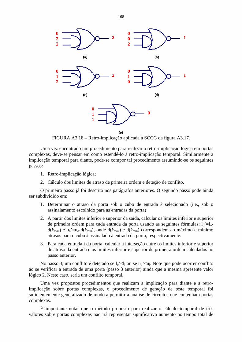
168
022
2
(a)
002
1
(b)
012
2
(c)
010
1
(d)
011
0
(e)
022
2
(a)
002
1
(b)
022
2
(a)
022
2022
2
(a)
002
1
(b)
002
1002
1
(b)
012
2
(c)
010
1
(d)
012
2
(c)
012
2012
2
(c)
010
1
(d)
010
1010
1
(d)
011
0
(e)
011
0011
0
(e)
FIGURA A3.18 – Retro-implicação aplicada à SCCG da figura A3.17.
Uma vez encontrado um procedimento para realizar a retro-implicação lógica em portascomplexas, deve-se pensar em como estendê-lo à retro-implicação temporal. Similarmente àimplicação temporal para diante, pode-se compor tal procedimento assumindo-se os seguintespassos:
1. Retro-implicação lógica;
2. Cálculo dos limites de atraso de primeira ordem e deteção de conflito.
O primeiro passo já foi descrito nos parágrafos anteriores. O segundo passo pode aindaser subdividido em:
1. Determinar o atraso da porta sob o cubo de entrada k selecionado (i.e., sob oassinalamento escolhido para as entradas da porta)
2. A partir dos limites inferior e superior da saída, calcular os limites inferior e superiorde primeira ordem para cada entrada da porta usando as seguintes fórmulas: lo’=lo-d(kmax) e uo’=uo-d(kmin), onde d(kmax) e d(kmin) correspondem ao máximo e mínimoatrasos para o cubo k assinalado à entrada da porta, respectivamente.
3. Para cada entrada i da porta, calcular a interseção entre os limites inferior e superiorde atraso da entrada e os limites inferior e superior de primeira ordem calculados nopasso anterior.
No passo 3, um conflito é detetado se lo’<li ou se uo’<ui. Note que pode ocorrer conflitoao se verificar a entrada de uma porta (passo 3 anterior) ainda que a mesma apresente valorlógico 2. Neste caso, seria um conflito temporal.
Uma vez propostos procedimentos que realizam a implicação para diante e a retro-implicação sobre portas complexas, o procedimento de geração de teste temporal foisuficientemente generalizado de modo a permitir a análise de circuitos que contenham portascomplexas.
É importante notar que o método proposto para realizar o cálculo temporal de trêsvalores sobre portas complexas não irá representar significativo aumento no tempo total de
169
execução uma vez que, por razões tecnológicas, os projetistas costumam limitar a 4 o númerode transistores em série nas portas CMOS.
A3.5 Conclusão e Perspectivas Futuras
O tema central desta tese foi a análise de timing funcional (functional timing analysis -FTA) de circuitos combinacionais, com ênfase na aplicabilidade dos modelos e algoritmos deFTA a circuitos que contenham portas complexas. As contribuições desta tese dizem respeitotanto à teoria geral de FTA quanto à FTA com portas complexas.
Como contribuição fundamental, foi apresentada um ampla e sistemática revisão sobremodelos e algoritmos de análise de timing. Com o intuito de facilitar a compreensão dosdiversos aspectos da FTA, foi proposta uma nova taxonomia para a classificação dosalgoritmos de FTA. De acordo com esta taxonomia, os algoritmos de FTA podem serclassificados pelo número de caminhos tratados simultaneamente, quando dos testes desensibilização (sensibilização individual de caminhos, sensibilização concorrente de caminhosou abordagem mista), pelo método usado para determinar se as condições de sensibilizaçãosão satisfeitas ou não (baseado em ATPG, baseado em solvabilidade – SAT, outros) e pelocritério de sensibilização usado.
Ainda com relação à teoria de FTA, foi especulado que os circuitos síncronosimplementados com o uso da tecnologia CMOS estado-da-arte podem apresentar umcomportamento assíncrono impossível de ser apropriadamente capturado pelo modelo deatraso de transição. Isto significa que, a fim de evitar uma subestimativa do atraso do circuito,seria preferível calcular o atraso para seqüências de vetores do que para pares de vetores. Poroutro lado, na ausência de métodos eficientes capazes de utilizar o modelo de atraso paraseqüências de vetores, o modelo de atraso flutuante seria o único capaz de fornecer umaestimativa segura para o atraso dos circuitos. Esta argumentação também justifica o uso daanálise de timing funcional, uma vez que esta baseia-se essencialmente no modelo de atrasoflutuante.
Considerando-se os algoritmos de FTA, foram realizados experimentos com métodos deenumeração de caminhos que confirmaram a seriedade do chamado “problema de explosão decaminho”. Em função deste problema, os métodos que usam sensibilização individual decaminhos foram abandonados, cedendo lugar para os métodos que usam sensibilizaçãoconcorrente.
No que se refere à FTA com portas complexas, escolheu-se o algoritmo TrueD-F,proposto por Devadas et al., para servir de base para um algoritmo de sensibilizaçãoconcorrente baseado em ATPG e que seja capaz de tratar circuitos que contenham portascomplexas, sem requerer macroexpansão. Esta escolha foi motivada pela existência deinúmeras técnicas de aceleração de algoritmos de ATPG. Outro argumento que sustenta aescolha de um algoritmo baseado em ATPG advém dos problemas de desempenhoapresentados pelos algoritmos baseados em SAT, quando modelos de atraso mais realistas sãoadotados.
A contribuição mais importante desta tese para a análise de timing funcional concerne aextensão do cálculo temporal para o caso de portas complexas. No contexto do algoritmoTrueD-F, o cálculo temporal consiste em um conjunto de regras que são usadas para calcularos valores lógicos e os limites inferior e superior dos atrasos nas saídas das portas. De acordocom o método proposto, o cálculo dos valores temporais de uma porta complexa é levado a

170
cabo por um procedimento recursivo que avalia cada subárvore, iniciando pelas folhas. Paraum máximo de 4 transistores em série na rede PMOS e na rede NMOS, o número máximo desubárvores que qualquer SCCG pode apresentar é 11, incluindo a subárvore raiz.Considerando-se que a avaliação de uma única subárvore consiste no cálculo do valor lógico edos intervalos de atraso, pode-se esperar que, operando-se diretamente sobre portascomplexas, os tempos de execução serão, na pior das hipótese, equivalentes aos tempos deexecução para um método que faça uso de macroexpansão. Entretanto, vale mencionar que aaplicação de um algoritmo baseado em ATPG a uma rede macroexpandida pode levar a umaumento significativo no tempo de execução, uma vez que haverá forte tendência de aumentono número de linhas do circuito, e portanto, aumento no número de linhas que devem serjustificadas.
Outras contribuições importantes para a FTA com portas complexas resultam dainvestigação de modelos computacionais de atraso aplicáveis ao caso das portas complexas. Atabela de equivalência modo flutuante/modo de transição permite a identificação dos pares devetores contidos num dado vetor flutuante. Este tipo de tabela também conduziu àidentificação dos três modelos computacionais de atraso de portas válidos para o modoflutuante, quais sejam: modelo de atraso de vetor, modelo de atraso de subida/descida emodelo de atraso único. Apesar de ser o mais preciso, o modelo de atraso de vetor requer 2n
valores de atraso (ou pares de atrasos) por porta, onde n é o número de entradas da porta.Considerando-se SCCGs com não mais do que 4 transistores em série, o valor máximo para né 16, produzindo um total de 216= 65536 vetores flutuantes. Por outro lado, o modelo desubida/descida separa os vetores flutuantes em dois grupos, o que reduz para dois valores deatraso (ou dois pares) por porta, sem deixar de garantir um limite superior para o atraso daporta.
A identificação dos pares de vetores contidos num dado vetor flutuante é de grandeinteresse quando se deseja caracterizar o atraso das portas. No caso de se utilizar simulaçãoelétrica, apenas os pares de vetores capazes de provocar uma transição na saída da portaprecisam ser simulados. Para o caso de caracterização por meio de formulação analítica, amesma informação pode ser usada para se adaptar as fórmulas de modo a cobrir apenas ospares de vetores que são de interesse. Entretanto, a tarefa de identificação dos pares de vetorescapazes de provocar transição na saída de uma porta é, per se, uma tarefa difícil que demandamais investigação. Por outro lado, uma conclusão muito importante que pode ser derivada databela de equivalência é que o formato de atraso pino-a-pino, normalmente usado nacaracterização de células de bibliotecas standard-cells, conduz a uma subestimativa do atrasodas portas, uma vez que é capaz de considerar somente uma parte dos vetores flutuantes quepodem causar transição na saída das portas.
Finalmente, a partir da tabela de equivalência modo flutuante/modo de transição, foipossível introduzir o conceito de atraso flutuante de um cubo, generalizando assim o modelode atraso de vetor.
A implicação temporal para diante para portas complexas faz uso de um procedimentoque calcula o valor temporal das portas. Conforme já argumentado, espera-se que acomplexidade de execução de tal procedimetno seja, no máximo, equivalente àquelaresultante de se operar sobre circuitos macroexpandidos. A retro-implicação temporal comportas complexas, por seu turno, não pode ser derivada diretamente da retro-implicação comportas simples porque os conceitos de valor controlante/valor não-controlante não pode seraplicado diretamente sobre as portas complexas. Assim, o método proposto consiste em usar omesmo procedimento da implicação temporal para diante, porém seguindo a filosofia doalgoritmo PODEM, ou seja, usando simulação de cubos sobre cada porta. O tempo de

171
execução para a simulação de cubos é, no pior caso, proporcional ao espaço das entradas daporta. Por exemplo, o espaço das entradas de uma SCCG com 4 transistores em série em cadauma das redes é de, no máximo, 216= 65536 vetores flutuantes. Obviamente, isto afeta otempo de execução do algoritmo de FTA como um todo.
Esta tese mostrou que é possível realizar FTA de circuitos que contenham portascomplexas usando a abordagem baseada em ATPG, com sensibilização concorrente decaminhos, sem o uso de macroexpansão. A principal vantagem de tal abordagem é a potencialredução no número de linhas do circuito que precisam ser justificadas, em comparação com aabordagem que usa macroexpansão. Apesar disso, a retro-implicação tende a sersignificativamente mais complexa sobretudo nos casos em que houver a presença de portascomplexas com significativo número de entradas. Este efeito pode ser minimizado pelo uso demétricas de testabilidade para guiar a exploração do espaço de entradas.
Finalmente, a extensão proposta para o cálculo temporal, juntamente com os modelos deatraso válidos para o modo flutuante, formam um conjunto de regras de macromodelamentoque abrem a possibilidade para se realizar uma “computação hierárquica do atraso flutuante”de circuitos. Esta é a conseqüência do conceito de porta complexa constituir umarepresentação genérica de qualquer porção possível de circuito CMOS.
O desempenho da abordagem proposta depende grandemente da habilidade doalgoritmo em tomar decisões acertadas. Tal qualidade pode ser incorporada através do uso demedidas de testabilidade, conforme feito pelos algoritmos PODEM e FAN. Assim, cálculosde testabilidade para portas complexas constituem um ponto a ser abordado no futuropróximo.
Os estudos de modelos computacionais de atraso válidos ajudou a preencher a lacunaque existe entre modelos físicos e modelos computacionais de atraso. Porém, há aindadiversos pontos que necessitam de maior investigação. Um destes corresponde à identificaçãoautomática dos pares de vetores responsáveis por transições nas saídas de uma dada porta.Outro ponto importante é o próprio método de caracterização do atraso, seja pelo uso desimulação elétrica, seja pelo uso/desenvolvimento de modelos analíticos. Um terceiro pontodiz respeito ao máximo número de entradas para as portas complexas, fator este queinfluencia diretamente o desempenho do método de FTA proposto: um número elevado deentradas por porta pode inviabilizar o uso do modelo de atraso de vetor, o qual tende a ser omais preciso. A limitação do número de transistores em série para 4 é uma estratégianormalmente adotada pelos projetistas para garantir o desempenho elétrico do circuito. Masainda com tal limitação, há 3503 possibilidades de SCCGs. Um trabalho útil consiste eminvestigar um limite prático no número de componentes das bibliotecas (virtual) de SCCGs,com base no desempenho das ferramentas de mapeamento tecnológico do estado-da-arte.
A abordagem proposta deve ser comparada com a abordagem baseada emmacroexpansão, em termos de tempo de execução e precisão, para certificar-se que a reduçãono número de linhas a serem justificadas se sobrepõe ao aumento de complexidade associadoaos procedimentos de implicação aplicados a portas complexas.
Outro aspecto a ser investigado é o desempenho e a precisão de uma computaçãohierárquica do atraso flutuante. Em uma primeira aproximação, pode-se esperar que o uso domodo hierárquico permita a análise de circuitos com complexidade de uma a duas ordens degrandeza maior do que no modo plano. Porém, é necessário investigar a influência dosmodelos computacionais de atraso de porta sobre a estimativa de atraso resultante no modohierárquico.

172
Por fim, um trabalho futuro de grande envergadura consiste em estabelecer uma amplacomparação entre a abordagem proposta, que é baseada em ATPG, e alguma abordagembaseada em SAT. Neste trabalho, uma dificuldade básica reside em se escolher um conjuntode modelos computacionais de atraso que sejam válidos para ambas abordagens e ao mesmotempo propiciem estimativas de atraso com precisão aceitável. Outra dificuldade reside emescolher algum algoritmo de FTA (ou ferramenta) baseada em SAT que seja capaz de tratarportas complexas.

173
References
[ABR90] ABRAMOVICI, M.; BREUER, M.; FRIEDMAN, A. Digital Systems Testingand Testable Design. Piscataway, NJ: IEEE Press, 1990. 652p.
[ASH95] ASHAR, Pranav; MALIK, Sharad. Functional Timing Analysis Using ATPG.IEEE Transactions on Computed-Aided Design of Integrated Circuits andSystems, Los Alamitos, California, v.14, n.8, p.1025-1030, August 1995.
[AUG89] AUGUSTIN, L. An Algebra of Waveforms. Stanford, California: ComputerSystems Laboratory, University of Stanford, Stanford, 1989. Technical Report.
[AUV90] AUVERGNE, D.; AZEMARD, N.; DESCHACHT, D.; ROBERT, M. InputWaveform Slope Effects in CMOS Delays. IEEE Journal of Solid-StateCircuits, Piscataway, NJ, CA, v.25, n.6, p.1588-1590, Dec. 1990.
[BAU88] BAUER, R. et al. XPSim: A MOS VLSI Simulator. In: IEEE/ACMINTERNATIONAL CONFERENCE ON COMPUTER-AIDED DESIGN, 1988.Santa Clara, California. Proceedings... Los Alamitos, California: IEEE ComputerSociety Press, 1988. p.66-69.
[BEN87] BENKOSKI, J. et al. Efficient Algorithms for Solving the False path Problem inTiming Verification In: IEEE/ACM INTERNATIONAL CONFERENCE ONCOMPUTER-AIDED DESIGN, 1987. Proceedings... Los Alamitos, California:IEEE Computer Society Press, 1987. p.44-47.
[BEN90] BENKOSKI, J.; VAN DEN MEERSCH, E.; CLAESEN, L.; DE MAN, H.Timing Verification Using Statically Sensitizable Paths. IEEE Transactions onCAD of Integrated Circuits and Systems, Los Alamitos, California, v.9, n.10,p.1073-1084, Oct. 1990.
[BEN91] BENKOSKI, J.; STEWART, R. TATOO: An industrial Timing Analyzer withFalse Path Elimination and Test Pattern Generation. In: EUROPEAN DESIGNAUTOMATION CONFERENCE, 1991. Los Alamitos, California: IEEEComputer Society, 1991. p.256-260.
[BER91] BERGAMASCHI, R. The Effects of False Paths in High-Level Synthesis. In:IEEE/ACM INTERNATIONAL CONFERENCE ON COMPUTER-AIDEDDESIGN, 1991, Santa Clara, California. Proceedings... Los Alamitos, California:IEEE Computer Society Press, 1991. p.80-83.
[BRA88] BRAND, D.; IYENGAR, V. Timing Analysis Using Functional Analysis. IEEETransactions on Computers, Piscataway, NJ, v.37, n.10, p.1309-1314, October1988
[CAD99] CADABRA. CLASSIC-SC Automated Transistor Layout Tool. Available at:<http://www.cadabradesign.com>. Visited on September 24, 1999.
174
[CHA75] CHAWLA, B. R.; GUMMEL, H. K.; KOZAK, P. MOTIS – An MOS TimingSimulator. IEEE Transactions on Circuits and Systems, Los Alamitos,California, v.CAS-22, n.12, p.901-909, December 1975.
[CHA93] CHANG, Hoon; ABRAHAM, Jacob A. VIPER: An Efficient VigorouslySensitizable Path Extractor. In: ACM/IEEE DESIGN AUTOMATIONCONFERENCE, 30., 1993, Dallas, Texas. Proceedings... Los Alamitos,California: IEEE Computer Society Press, 1993. p.112-117.
[CHA96] CHANDRAMOULI, V.; SAKALLAH, Karem A. Modeling the Effects ofTemporal Proximity of Input Transitions on Gate Propagation Delay andTransition Time. In: ACM/IEEE DESIGN AUTOMATION CONFERENCE, 33.,1996, Las Vegas, Nevada. Proceedings... Los Alamitos, California: IEEEComputer Press, 1996. p.617-622.
[CHE91] CHEN, H.-C.; DU, D. Path Sensitization in Critical Path Problem. In:IEEE/ACM INTERNATIONAL CONFERENCE ON COMPUTER-AIDEDDESIGN, 1991, Santa Clara, California. Proceedings... Los Alamitos, California:IEEE Computer Society Press, 1991. p.208-211.
[CHE93] CHEN, H.-C.; DU, D. Path Sensitization in Critical Path Problem IEEETransactions on CAD of Integrated Circuits and Systems, Los Alamitos,California, v.12, n.2, p.196-207, February 1993.
[CHE93a] CHEN, H.-C.; DU, D. Critical Path Selection for Performance OptimizationIEEE Transactions on CAD of Integrated Circuits and Systems, LosAlamitos, California, v.12, n.2, p.185-195, February 1993.
[CHE94] CHENG, S.; CHEN, H.-C.; DU, D.; LIM, A. The Role of Long and Short Pathsin Circuit Performance Optimization IEEE Transactions on CAD of IntegratedCircuits and Systems, Los Alamitos, California, v.13, n.7, p.857-864, July 1994.
[CHS93] CHENG, S.; CHEN, H.-C.; HSU, Y.-C.; DU, D. A Path Sensitization Approachto area Reduction In: INTERNATIONAL CONFERENCE ON COMPUTERDESIGN: VLSI IN COMPUTERS AND PROCESSORS, 1993, Cambridge(Mas.). Proceedings... Los Alamitos, California: IEEE, 1993. p.73-76.
[COR90] CORMEN, Thomas H.; LEISERSON, Charles E.; RIVEST, Ronald L.Introduction to Algorithms. Cambridge: MIT, 1990.
[DAG96] DAGA, J.-M.; TURGIS, S.; AUVERGNE, D. Design Oriented Standard CellDelay Modeling. In: INTERNATIONAL WORKSHOP ON POWER ANDTIMING MODELING, OPTIMIZATION AND SIMULATION, PATMOS, 1996.Bologna, Italy. Proceedings... Bologna, Italy: Pitagora Editrice Bologna, 1996.p.265-274.
[DAG99] DAGA, J.-M.; AUVERGNE, D. A Comprehensive Delay Macro Modeling forSubmicrometer CMOS Logics. IEEE Journal of Solid-State Circuits,Piscataway, NJ, v.34, n.1, p.42-55, Jan. 1999.

175
[DES88] DESCHACHT, D.; ROBERT, M.; AUVERGNE, D. Explicit Formulation ofDelays in CMOS Data Paths. IEEE Journal of Solid-State Circuits,Piscataway, NJ, v.23, n.5, p.1257-1264, October 1988.
[DET87] DETJENS, E.; GANNOT, G.; RUDELL, R. L. Technology Mapping in MIS. In:IEEE/ACM INTERNATIONAL CONFERENCE ON COMPUTER-AIDEDDESIGN, 1987. Proceedings... Los Alamitos, California: IEEE Computer SocietyPress, 1987. p.116-119.
[DEV91] DEVADAS, S.; KEUTZER, K.; MALIK, S. Delay Computation inCombinational Logic Circuits: Theory and Algorithms. In: IEEE/ACMINTERNATIONAL CONFERENCE ON COMPUTER-AIDED DESIGN, 1991,Santa Clara, California. Proceedings... Los Alamitos, California: IEEE ComputerSociety Press, 1991. p.176-179.
[DEV92] DEVADAS, S.; KEUTZER, K.; MALIK, S.; WANG, A. Certified TimingVerification and the Transition Delay of a Logic Circuit. In: ACM/IEEE DESIGNAUTOMATION CONFERENCE, 29., 1992, Anaheim, California. Proceedings...Los Alamitos, California: IEEE Computer Society Press, 1992. p.549-555.
[DEV93] DEVADAS, S.; KEUTZER, K.; MALIK, S. Computation of Floating ModeDelay in Combinational Circuits: Theory and Algorithms. IEEE Transactions onComputed-Aided Design of Integrated Circuits and Systems, Los Alamitos,California, v.12, n.12, p.1913-1923, Dec. 1993.
[DEV93a] DEVADAS, S.; KEUTZER, K.; MALIK, S.; WANG, A. Computation ofFloating Mode Delay in Combinational Circuits: Practice and Implementation.IEEE Transactions on Computed-Aided Design of Integrated Circuits andSystems, Los Alamitos, California, v.12, n.12, p.1924-1936, December 1993.
[DEV94] DEVADAS, S.; GHOSH, A.; KEUTZER, K. Logic Synthesis. New York:McGraw-Hill, 1994. 404p.
[DEV94a] DEVADAS, S.; KEUTZER, K.; MALIK, S.; WANG, A. Certified TimingVerification and the Transition Delay of a Logic Circuit. IEEE Transactions onVery Large Scale Integration (VLSI) Systems, Los Alamitos, California, v.2,n.3, p.333-342, September 1994.
[DEV94b] DEVADAS, S.; KEUTZER, K.; MALIK, S.; WANG, A Event Suppression:Improving the Efficiency of Timing Simulation for Synchronous Digital Circuits.IEEE Transactions on Computed-Aided Design of Integrated Circuits andSystems, Los Alamitos, California, v.13, n.6, p.814-822, June 1994.
[DU89] DU, David H. C.; YEN, Steve H. C.; GHANTA, S. On the General False PathProblem in Timing Analysis In: ACM/IEEE DESIGN AUTOMATIONCONFERENCE, 26., 1989, Las Vegas, Nevada. Proceedings... Los Alamitos,California: IEEE Computer Society Press, 1989. p. 555-560.
[EIJ94] EIJNDHOVEN, J.T.J. van. CMOS cell generation for Logic Synthesis. In:INTERNATIONAL CONFERENCE ON ASICS, ASICON, 1994, Beijing, China.Proceedings... Beijing, China: Electr. Ind. Publishing House, 1994. p. 75-78.

176
[ELM48] ELMORE, W. C. The Transient Response of Damped Linear Networks withParticular Regard to Wide-Band Amplifiers. Journal of Applied Physics, NewYork, v.19, n.1, p.55-63, Jan. 1948.
[FOR97] FORZAN, C.; FRANZINI, B.; GUARDIANI, C. Accurate and EfficientMacromodel of Submicron Digital Standard Cells. In: ACM/IEEE DESIGNAUTOMATION CONFERENCE, 34., 1997, Anaheim, California. Proceedings...Los Alamitos, California: IEEE Computer Society Press, 1997. p.633-637.
[GOE81] GOEL, Prabhakar. An Implicit Enumeration Algorithm to Generate Tests forCombinational Logic Circuits. IEEE Transactions on Computers, Piscataway,NJ, v.C-30, n.3, p.215-222, Mar. 1981.
[GAJ99] GAJSKI, D. Principles of Logic Design. New Jersey: Prentice Hall, 1999. 447p.
[GÜN98] GÜNTZEL, José L.; PINTO, Ana Cristina M.; REIS, Ricardo A. L. ImprovingPath Enumeration Accuracy by Considering Different Fall and Rise Gate Delays.In: WORKSHOP IBERCHIP 4., 1998, Mar del Plata, Argentina. Memorias...Buenos Aires: IBERCHIP/Universidad Nacional de La Plata, 1998. p.91-100.
[GÜN98a] GÜNTZEL, José Luís; PINTO, Ana Cristina M.; REIS, Ricardo. ConsideringDifferent Fall and Rise Gate Delays in Path Enumeration. In: UFRGSMICROELECTRONICS SEMINAR, 13., 1998, Bento Gonçalves, Brazil.Proceedings... Porto Alegre, Brazil: UFRGS, 1998. 196p. p.59-65.
[GÜN98b] GÜNTZEL, José L. et al. An Improved Path Enumeration Method ConsideringDifferent Fall and Rise Gate Delays. In: BRAZILIAN SYMPOSIUM ONINTEGRATED CIRCUIT DESIGN, SBCCI, 11., 1998, Búzios, Brazil.Proceedings... Los Alamitos, California: IEEE Computer Society, 1998. p.208-211.
[GÜN99] GÜNTZEL, José L. et al. Path Enumeration Algorithms for Timing Analysis ofDigital Circuits. In: WORKSHOP IBERCHIP, 5., 1999, Lima, Peru. Memorias...Lima, Peru: IBERCHIP/Pontificia Universidad Católica del Perú, 1999. p.334-341.
[GÜN99a] GÜNTZEL, José Luís; DALL PIZZOL, Guilherme M.; REIS, Ricardo. ExploitingCircuit Regularity in Functional Timing Analysis. In: UFRGSMICROELECTRONICS SEMINAR, 14., 1999, Pelotas, Brazil. Proceedings...Porto Alegre, Brazil: UFRGS, 1999. 175p. p.77-82.
[GUR97] GURUSWAMY, M. et al. Cellerity: A Fully Automatic Layout Synthesis Systemfor Standard Cell Libraries. In: ACM/IEEE DESIGN AUTOMATIONCONFERENCE, 34., 1997, Anaheim, California. Proceedings... Los Alamitos,California: IEEE Computer Society Press, 1997. p.327
[HIR98] HIRATA, A.; ONODERA, H.; TAMARU, K. Proposal of a Timing Model forCMOS Logic Gates Driving a CRC π Load. In: ACM/IEEE INTERNATIONALCONFERENCE ON COMPUTER-AIDED DESIGN, 1998, Santa Clara,California. Proceedings… Los Alamitos, California: IEEE Computer SocietyPress, 1998. p.537-544.

177
[HIT82] HITCHCOCK, R. B. Timing Verification and the Timing Analysis Program. In:ACM/IEEE DESIGN AUTOMATION CONFERENCE, 19., 1982, Las Vegas,Nevada. Proceedings... Los Alamitos, California: IEEE Computer Society Press,1982. p.594-604.
[HOR84] HOROWITZ, M. Timing Models for MOS Circuits. Stanford, California:Stanford University, 1984. 120p. Ph.D. Thesis.
[HRA78] HRAPCENKO, V. Depth and Delay in a Network. Soviet Math. Dokl.,[ S.l.],v.19, n.4, p.1006-1009, 1978.
[HUA94] HUANG, Shiang-Tang; PARNG, Tai-Ming; SHYU; Jyou-Min Timed BooleanCalculus and Its Applications in Timing Analysis. IEEE Transactions onComputer-Aided Design of Integrated Circuits and Systems, Los Alamitos,California, v.13, n.7, p.875-883, July 1994.
[HSU98] HSU, Y.-C.; CHEN, H.-C.; SUN, S.; DU, D. Timing Analysis of CombinationalCircuits Containing Complex Gates. In: INTERNATIONAL CONFERENCE ONCOMPUTER DESIGN: VLSI IN COMPUTERS AND PROCESSORS, 1998,Austin, Texas. Proceedings... Los Alamitos, California: IEEE, 1998. p.407-412
[JOU87] JOUPPI, Norman P. Timing Analysis and Performance Improvement of MOSVLSI Designs. IEEE Transactions on Computer-Aided Design, Los Alamitos,California, v.CAD-6, n.4, p.650-665, July 1987.
[JU91] JU, Y.-C.; SALEH, R. Incremental Techniques for the Identification of StaticallySensitizable Critical Paths. In: ACM/IEEE DESIGN AUTOMATIONCONFERENCE, 28., 1991, San Francisco, California. Proceedings... New York:IEEE, 1991. p.541-546.
[KEU91] KEUTZER, K.; MALIK, S.; SALDANHA, A. Is Redundancy Necessary toReduce Delay? IEEE Transactions on Computer-Aided Design of IntegratedCircuits and Systems, Los Alamitos, California, v.10, n.4, p.427-435, April1991.
[KIM86] KIM, Y. H. ELOGIC: A Relaxation-Based Switch-Level SimulationTechnique. Berkeley, California: University of California, Department ofElectrical Engineering and Computer Sciences, 1986. 39p. (UCB/ERL M86/2).
[KIM98] KIM, Juho; DU, David H.C. Performance Optimization by Gate Sizing and PathSensitization. IEEE Transactions on CAD of Integrated Circuits and Systems,Los Alamitos, California, v.17, n.5, p.459-462, May 1998.
[KIR66] KIRKPATRICK, T. W.; CLARCK, N. Pert as an Aid to Logic Design. IBMJournal of Research and Development, Armonk, v.10, n.2, p.135-141, March1966.
[KUK97] KUKIMOTO, Y. et al. Approximate Timing Analysis of Combinational Circuitsunder the XBD0 Model. In: ACM/IEEE INTERNATIONAL CONFERENCE ONCOMPUTER-AIDED DESIGN, 1997, San Jose, California Proceedings... LosAlamitos, California: IEEE Computer Society Press, 1997. p.176-181.
178
[KUK97a] KUKIMOTO, Y.; BRAYTON, R. Removing False Paths from CombinationalModules. In: ACM/IEEE INTERNATIONAL WORKSHOP ON TIMINGISSUES IN SPECIFICATION AND SYNTHESIS OF DIGITAL SYSTEMS,TAU, 1997. Proceedings... [S.l.:s.n.], 1997.
[LAM93] LAM, W.; BRAYTON, R.; SANGIOVANNI-VINCENTELLI, A. Circuit DelayModels and Their Exact Computation Using Timed Boolean Functions. In:ACM/IEEE DESIGN AUTOMATION CONFERENCE, 30., 1993, Dallas, Texas.Proceedings... Los Alamitos, California: IEEE Computer Society Press, 1993.p.128-134.
[LAM94] LAM, W.; BRAYTON, R. Timed Boolean Functions: A Unified Formalism forExact Timing Analysis. Norwell, MA: Kluwer Academic Publishers, 1994. 273p.
[LAR92] LARRABEE, T. Test Pattern Generation Using Boolean Satisfiability. IEEETransactions on CAD of Integrated Circuits and Systems, Los Alamitos,California, v.11, n.1, p.4-15, Jan. 1992.
[LEL82] LELARASMEE, E.; SANGIOVANNI-VICENTELLI, A. RELAX: A NewCircuit Simulator for Large Scale MOS Integrated Circuits. In: ACM/IEEEDESIGN AUTOMATION CONFERENCE, 19., 1982, Las Vegas, Nevada.Proceedings... Los Alamitos, California: IEEE Computer Society Press, 1982.p.682-690.
[LIM99] LIMA, Fernanda Gusmão de. Projeto com Matrizes de Células LógicasProgramáveis. Porto Alegre: Instituto de Informática da UFRGS, 1999. 123p.Dissertação de Mestrado.
[LI89] LI, W.; REDDY, S.; SAHNI, S. On Path Selection in Combinational LogicCircuits. IEEE Transactions on CAD of Integrated Circuits and Systems, LosAlamitos, California, v.8, n.1, p.56-63, Jan. 1989.
[LIN94] LIN, H.-R.; HWANG, T-T. Dynamical Identification of Critical Paths for IterativeGate Sizing. In: IEEE/ACM INTERNATIONAL CONFERENCE ONCOMPUTER-AIDED DESIGN, 1994, Santa Clara , California. Proceedings...Los Alamitos, California: IEEE Computer Society Press, 1994. p.481-484.
[LIN95] LIN, H.-R.; HWANG, T-T. Power Reduction by Gate Sizing with Path-OrientedSlack Calculation. In: ASIAN AND SOUTHERN PACIFIC DESIGNAUTOMATION CONFERENCE, 1995, August Chiba, Japan. Proceedings...[S.l.]: SIGDA, 1995. p.7-12.
[LOP80] LOPEZ, A.D.; LAW, H.S. A Dense Gate Matrix Layout Method for MOS VLSI.IEEE Transactions on Electron Devices, New York, v.ED-27, n.8 p.1671-1675,Aug. 1980.
[MCG89] MCGEER, P.; BRAYTON, R. Efficient Algorithms for Computing the LongestViable Path in a Combinational Circuit In: ACM/IEEE DESIGN AUTOMATIONCONFERENCE, 26., 1989, Las Vegas, Nevada. Proceedings... Los Alamitos,California: IEEE Computer Press, 1989. p.561-567.

179
[MCG91] MCGEER, P.; BRAYTON, R. Integrating Functional and Temporal Domainsin Logic Design: The False Path Problem and its Implications. Norwell, MA:Kluwer Academic Publishers, 1991. 212p.
[MCG91a] MCGEER, P. et al. Timing Analysis and Path Delay-Fault Test Generation usingPath-Recursive Functions. In: IEEE/ACM INTERNATIONAL CONFERENCEON COMPUTER-AIDED DESIGN, 1991, Santa Clara, California. Proceedings...Los Alamitos, California: IEEE Computer Society Press, 1991. p.180-183.
[MCG93] MCGEER, P. et al. Delay Models and Exact Timing Analysis. In: SASAO, T.(Ed.). Logic Synthesis and Optimization. Norwell, MA: Kluwer AcademicPublishers, 1993. p.167-189.
[MOR94] MORAES, Fernando. Synthèse Topologique de Macro-Cellules en TechnologieCMOS. Montpellier, France: Université Montpellier II, 1994. Thèse de Doctorat.
[MOR97] MORAES, F.; REIS, R.; LIMA F. An Efficient Layout Style for Three-MetalCMOS Macro-Cells. In: REIS, R.; CLAESEN, L. (Ed.). VLSI: IntegratedSystems on Silicon. London: Chapman & Hall, 1997. p.415-426.
[NAG75] NAGEL, W. SPICE2, A Computer Program to Simulate SemiconductorCircuits. Berkeley, California: University of California, Department of ElectricalEngineering and Computer Sciences, 1975. 63p. (UCB/ERL M75/520).
[NEM98] NEMANI, M.; NAJM, F. Delay Estimation of VLSI Circuits from a High-LevelView In: ACM/IEEE DESIGN AUTOMATION CONFERENCE, 35., 1998, SanFrancisco, California. Proceedings... Los Alamitos, California: IEEE ComputerSociety Press, 1998. p.591-594.
[OUS85] OUSTERHOUT, John K. A Switch-Level Timing Verifier for Digital MOSVLSI, IEEE Transactions on Computer-Aided Design, Los Alamitos,California, v. CAD-4, n. 3, p.336-349, July 1985.
[PER89] PERREMANS, S.; CLAESEN, L.; DE MAN, H. Static Timing Analysis ofDynamically Sensitizable Paths. In: ACM/IEEE DESIGN AUTOMATIONCONFERENCE, 26., 1989, Las Vegas, Nevada. Proceedings... Los Alamitos,California: IEEE Computer Society Press, 1989. p.568-573.
[PES94] PESET LLOPIS, R. Exact Path Sensitization in Timing Analysis In:EUROPEAN DESIGN AUTOMATION CONFERENCE, 1994, Grenoble.Proceedings... Los Alamitos: IEEE, 1994. p.380-385.
[PIN98] PINTO, Ana Cristina M.; GÜNTZEL, José Luís; REIS, Ricardo. PerformanceEvaluation of the sgd and spgd Path Enumeration Methods. In: UFRGSMICROELECTRONICS SEMINAR, 13., 1998, Bento Gonçalves, Brazil.Proceedings... Porto Alegre, Brazil: UFRGS, 1998. 196p. p.67-72.
[PRA00] PRADO, A.; LUBASZEWSKI, M.; REIS, A. Identifying Stuck-at Faults withVertex Precedent BDDs. In: WORKSHOP IBERCHIP, 6., 2000, São Paulo,Brazil. Anais... São Paulo, Brazil: CTI/CYTED, 2000. 196p. p.235-244.

180
[RAB96] RABAEY, Jan. M. Digital Integrated Circuits: a Design Perspective. UpperSaddle River, New Jersey: Prentice Hall, 1996. chapter 4, p.210-222.
[RAT94] RATZLAFF, C. L.; PILLAGE, L. T. RICE: Rapid Interconnect CircuitEvaluation Using AWE. IEEE Transactions on Computer-Aided Design ofIntegrated Circuits and Systems, Los Alamitos, California, v.13, n.6, p.763-776,June 1994.
[RIE96] RIERA i BABURÉS, Jordi. Mapatge Tecnològic Orientat a Generadors deMòduls. Bellaterra, Espanya: Universitat Autònoma de Barcelona, 1996. TesiDoctoral.
[REI95] REIS, André I. et al. Associating CMOS Transistors with BDD Arcs forTechnology Mapping. IEE Electronic Letters, London, v.31, n.14, p.1118-1120,July 1995.
[REI97] REIS, André I. et al. Library Free Technology Mapping. In: REIS, R.;CLAESEN, L. (Ed.). VLSI: Integrated Systems on Silicon. London: Chapman &Hall, 1997. p.303-314.
[REI98] REIS, André I. Assignation Technologique sur Biblioteques Virtuelles dePortes Complexes CMOS. Montpellier: Université Montpellier II, 1998. 122p.Thèse de Doctorat.
[REI99] REIS, Ricardo A. L. FUCAS: FUll Custom Layout Synthesis. Available at:<http://www.inf.ufrgs.br/~reis/rese99.html>. Visited on September 23, 1999.
[ROT66] ROTH, J.P. Diagnosis of Automata Failures: A Calculus and a New Method In:IBM Journal of Research and Development, Armonk, v.10, n.6, p.278-291,July1966.
[RUB83] RUBINSTEIN, J.; PENFIELD, P. Jr.; HOROWITZ, M. A. Signal Delay in RCTree Networks. IEEE Transactions on Computer-Aided Design, Los Alamitos,California, v.CAD-2, n.3, p.202-210, July 1985.
[SAK83] SAKURAI, Takayasu Approximation of Wiring Delay in MOSFET LSI. IEEEJournal of Solid-State Circuits, Piscataway, NJ, v.SC-18, n.4, p.418-426,August 1983.
[SAK88] SAKURAI, Takayasu. CMOS Inverter Delay and Other Formulas Using α-PowerLaw MOS Model. In: ACM/IEEE INTERNATIONAL CONFERENCE ONCOMPUTER-AIDED DESIGN, 1988, Santa Clara, California. Proceedings…Los Alamitos, California: IEEE Computer Society Press, 1988. p.74-76.
[SAL94] SALDANHA, A.; BRAYTON, R.; SANGIOVANNI-VICENTELLI, A. CircuitStructure Relations to Redundancy and Delay. IEEE Transactions on CAD ofIntegrated Circuits and Systems, Los Alamitos, California, v.13, n.7, p.875-883,July 1994.

181
[SEG89] SEGER, Carl-Johan. A Bounded Delay Race Model. In: IEEE/ACMINTERNATIONAL CONFERENCE ON COMPUTER-AIDED DESIGN, 1989,Santa Clara, California. Proceedings... Los Alamitos, California: IEEE ComputerSociety Press, 1989. p.130-133.
[SEN92] SENTOVICH, E. M. et al. SIS: A System for Sequential Circuit Synthesis.Berkeley, California: Electronics Research Laboratory, University of California.May 1992. 45p. (Memorandum No UCB/ERL N92/41)
[SIL93] SILVA, João P.M.; SAKALLAH, Karem. Concurrent Path Sensitization inTiming Analysis. In: THE EUROPEAN CONFERENCE ON DESIGNAUTOMATION WITH THE EUROPEAN EVENT IN ASIC DESIGN, 1993,Paris, France. Proceedings... Los Alamitos, California: IEEE Computer SocietyPress, 1993.
[SIL93a] SILVA, João P.M.; SAKALLAH, Karem. An Analysis of Path SensitizationCriteria. In: INTERNATIONAL CONFERENCE ON COMPUTER DESIGN:VLSI IN COMPUTERS AND PROCESSORS, 1993, Cambridge, MA.Proceedings... Los Alamitos, California: IEEE, 1993. p.68-72.
[SIL94] SILVA, João P.M.; SAKALLAH, Karem. Efficient and Robust Test Generation-Based Timing Analysis. In: IEEE INTERNATIONAL SYMPOSIUM ONCIRCUITS AND SYSTEMS, 1994, London. Proceedings... Piscataway: IEEE1994. v.1, p.303-306.
[SIL94a] SILVA, João P.M.; SAKALLAH, Karem. Dynamic Search-Space PruningTechniques in Path Sensitization. In: ACM/IEEE DESIGN AUTOMATIONCONFERENCE, 31., 1994, San Diego, California. Proceedings... Los Alamitos,California: IEEE Computer Society Press, 1994.
[SIL96] SILVA, João P.M.; SAKALLAH, Karem. GRASP – A New Search Algorithm forSatisfiability. In: IEEE INTERNATIONAL SYMPOSIUM ON CIRCUITS ANDSYSTEMS, 1996, San Jose, California. Proceedings... Los Alamitos, California:IEEE Computer Society Press, 1996. p.220-227.
[SIL98] SILVA, Luís Guerra et al. Realistic Delay Modeling in Satisfiability-BasedTiming Analysis. In: IEEE INTERNATIONAL SYMPOSIUM ON CIRCUITSAND SYSTEMS, 1998. Proceedings... Piscataway: IEEE, 1998. v.6, p.215-218.
[SIL99] SILVA, Luís Jorge B. M. G. e. Models and Algorithms for Timing Analysis ofCombinational Circuits. Lisboa: Instituto Superior Técnico (IST), UniversidadeTécnica de Lisboa, 1999. 84p. Master Dissertation.
[SUN94] SUN, Shang-Zhi; DU, David H.C.; CHEN, Hsi-Chuan. Efficient Timing Analysisof CMOS Circuits Considering Data Dependent Delays. In: IEEE/ACMINTERNATIONAL CONFERENCE ON COMPUTER-AIDED DESIGN, 1994,Santa Clara, California. Proceedings... Los Alamitos, California: IEEE ComputerSociety Press, 1994. p.156-159.
[UEB95] UEBEL, Luis Felipe. Verificação de Timing em Circuitos VLSI CMOSDigitais. Porto Alegre: CPGCC da UFRGS, 1995. 222p. Dissertação de Mestrado.

182
[UEH81] UEHARA, T.; CLEEMPUT, W.M. Optimal Layout of CMOS Functional Arrays.IEEE Transactions on Computers, Piscataway, NJ, v.C-30, n.5, p.305-312, May1981
[YAL95] YALCIN, H.; HAYES, J. Hierarchical Timing Analysis Using ConditionalDelays. In: IEEE/ACM INTERNATIONAL CONFERENCE ON COMPUTER-AIDED DESIGN, 1995, Santa Clara, California. Proceedings... Los Alamitos,California: IEEE Computer Society Press, 1995.
[YEN88] YEN, S.; GHANTA, S.; DU, D. A Path Selection Algorithm for Timing AnalysisIn: ACM/IEEE DESIGN AUTOMATION CONFERENCE, 25., 1988.Proceedings... Los Alamitos, California: IEEE Computer Society Press, 1988.p.720-723.
[YEN89] YEN, S.; DU, D.; GHANTA, S. Efficient Algorithms for Extracting the K MostCritical Paths in Timing Analysis In: ACM/IEEE DESIGN AUTOMATIONCONFERENCE, 26., 1989, Las Vegas, Nevada. Proceedings... Los Alamitos,California: IEEE Computer Society Press, 1989. p.649-652.
[YEN91] YEN, S.; DU, D.; GHANTA, S. Efficient Algorithms for Extracting the K MostCritical Paths in Timing Analysis. International Journal of Computer AidedVLSI Design,[ S.l.],v.3, n.2, p.193-215, 1991.
[WIS84] WISTON, Patrick H. Altificial Intelligence. 2nd ed. Reading, Massachusetts:Addison-Wesley Publishing Company, 1984. 524p.