fundamental material properties - cornell...
TRANSCRIPT

• Dielectric Constant
• Thermal Expansion Coefficient
• Thermal Conductivity
• Processing Temperature
• Decomposition Temperature
Fundamental Material Properties

HyperBGA
HyperBGA is a registered trademark of Endicott Interconnect

ASIC* (ay-sik)
Short for Application-Specific Integrated Circuit.
A chip designed for a particular application (as opposed to the integrated circuits that control functions such as RAM in a PC).ASICs are built by connecting existing circuit building blocks in new ways. Since the building blocks already exist in a library, it is much easier to produce a new ASIC than to design a new chip from scratch. ASICs are commonly used in automotive computers to control the functions of the vehicle and in PDAs. ________________* As defined in http://www.webopedia.com/TERM/A/ASIC.html

0.750.55Coupled Noise (mV/mm @ 1V/ns)
11.55.6Delay (ps/mm)
0.270.11Capacitance (pF/mm)
3754Impedance (Zo) (W)
3012Line height (µm) nominal
9025Line width (µm) nominal
9.52.8Dielectric Constant
2550500Substrate Thickness (µm)
179Layers
AluminaCeramic
HyperBGA
Physical / Electrical Comparison
Ceramic is: thicker (5x), heavier and slower

Why low Dk ? Fast signal propagation time,
k
cD
υ =
11.81.0Air
8.12.1PTFE
5.64.4Epoxy/Glass
3.79.5Ceramic
υ(in/ns)
DkDielectric
Dklw
lsh1
h2
210.512
842.233
2412749
h2h1lslwDk
all physical dimensions in mils
all assume Zo = 50 ohms
…also thinner and more tightly spaced.
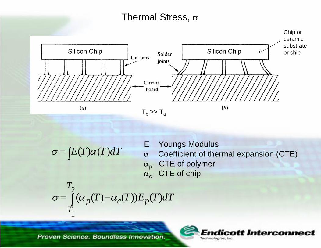
Thermal Stress, σ
Silicon Chip Silicon Chip
Tb >> Ta
( ) ( )E T T dTσ α=∫
2
1
( ( ) ( )) ( )T
p c pT
T T E T dTσ α α= −∫
E Youngs Modulusα Coefficient of thermal expansion (CTE)αp CTE of polymerαc CTE of chip
Chip or ceramicsubstrate or chip
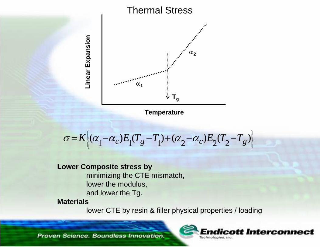
Thermal Stress
Temperature
Tg
α1
α2
Line
ar E
xpan
sion
1 1 1 2 2 2( ) ( ) ( ) ( )c g c gK E T T E T Tσ α α α α⎧ ⎫⎪ ⎪⎨ ⎬⎪ ⎪⎩ ⎭
= − − + − −
Lower Composite stress byminimizing the CTE mismatch,lower the modulus,and lower the Tg.
Materialslower CTE by resin & filler physical properties / loading

CTE Measurement: Thermal Mechanical Analysis
50.00°C
125.00°CAlpha=65.5µm/m°C
187.16°C
211.84°CAlpha=340.µm/m°C
171.17°C
-10
-5
0
5
10
15
Dim
ensi
on C
hang
e (µ
m)
0 50 100 150 200 250
Temperature (°C)
Sample: IBM DC ZSize: 0.5225 mmMethod: 5C/m 30-225 .1N scan 2Comment: 5C/m RT-225,LN2 cool to RT,5C/m RT-225 sc2
TMAFile: A:\gktmab.219Operator: G. Kohut T49Run Date: 13-Feb-2001 02:18p

Thermal Expansion Coefficient
0
5
10
15
20
25
30
-150 -50 50 150 250 350
Temperature (C)
TCE
(ppm
/ C
)
Cu Invar Cu Silica Filled PTFE Cu Si HyperBGA
HyperBGA
CIC*
Si
Cu
Silica-filled PTFE
TCE Data for Primary Materials in the HyperBGA Composite
* Invar is an alloy of Ni & Fe

2310Aluminum
1828Stainless 302
5 – 720CIC (Cu Invar Cu)
1717Plated Cu
400.6 – 0.9Outer layer dielectric
Softening> 125
20 – 25*0.03 – 0.10HyperBGA filled PTFE
110 – 13060 – 80*0.25 – 0.40PID soldermask
20016 – 17* 60 – 65
2.6 – 2.7BT w/ 2116 cloth
20055 – 60*0.4BT resin
644Alumina ceramic
319Glass ceramic
327Silicon die (crystal)
Tg°C
Effective TCEppm/ °C
Effective Modulus
Mpsi
Mechanical Properties of Packaging Materials
* Effective TCE below Tg
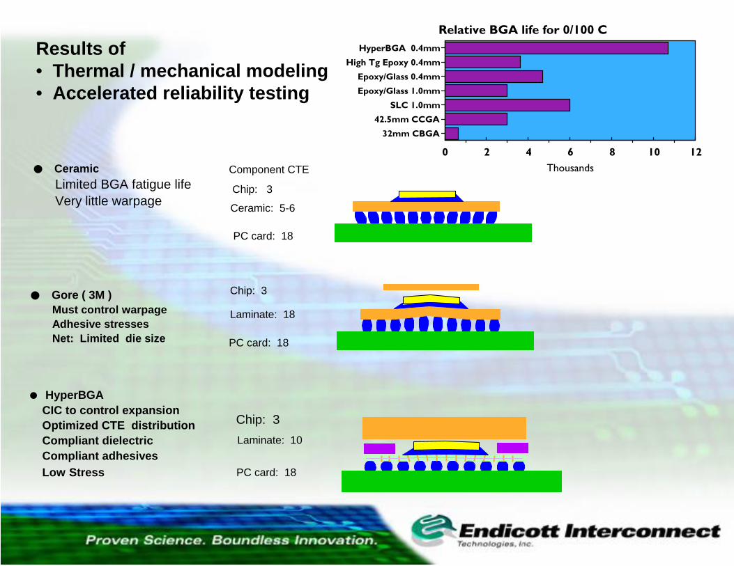
Ceramic Limited BGA fatigue lifeVery little warpage
Chip: 3
Ceramic: 5-6
PC card: 18
Component CTE
PC card: 18
Chip: 3
Laminate: 18
Gore ( 3M )Must control warpageAdhesive stressesNet: Limited die size
Chip: 3Laminate: 10
PC card: 18
HyperBGA CIC to control expansion Optimized CTE distribution Compliant dielectric Compliant adhesives Low Stress
HyperBGA 0.4mm
High Tg Epoxy 0.4mm
Epoxy/Glass 0.4mm
Epoxy/Glass 1.0mm
SLC 1.0mm
42.5mm CCGA
32mm CBGA
0 2 4 6 8 10 12
Thousands
Relative BGA life for 0/100 C
Results of• Thermal / mechanical modeling• Accelerated reliability testing
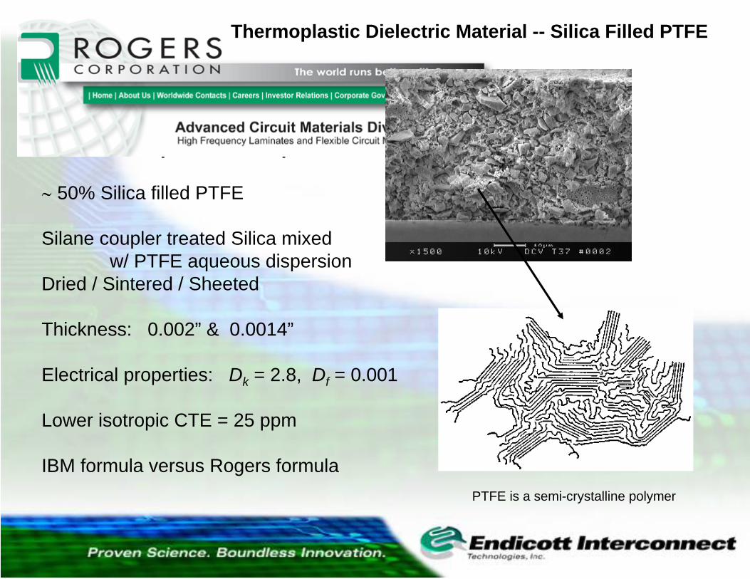
Material Composition / Properties
i 50% Silica filled PTFE
Silane coupler treated Silica mixed w/ PTFE aqueous dispersion
Dried / Sintered / Sheeted
Thickness: 0.002” & 0.0014”
Electrical properties: Dk = 2.8, Df = 0.001
Lower isotropic CTE = 25 ppm
IBM formula versus Rogers formulaPTFE is a semi-crystalline polymer
Thermoplastic Dielectric Material -- Silica Filled PTFE
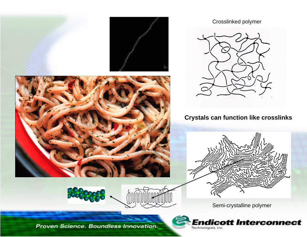
Semi-crystalline polymer
Crosslinked polymer
Crystals can function like crosslinks

HyperBGALaminate Build Process is Sequential
BGA pad
Ground CIC
Signal
Power
Microvia
Bump
Chip
Underfill
Soldermask
1st Inner PTFE
Filled PTH
3rd Outer PTFE
2nd Middle PTFE
• Inner Layer exposed to three laminations
• Outer Layer exposed to one lamination
What is effect of repeated laminations ?
Starts with Ground Plane
Inner layer PTFE is laminated
2nd layer laminated
Outer layer laminated

The Competition
MICROLAM® 600 Series Dielectrics
MICROLAM® 600 Series Microvia Dielectrics have optimized electrical and mechanical properties and consist of a non-woven, continuous toughening matrix and standard epoxy resins. Engineered to resist dielectric cracking and provide improved PCB mechanical reliability in cell phones, PDAs, and other portable devices, these high performance materials are processed using the same equipment and techniques as resin-coated copper and dry films.
Microlam is both thermoplastic &thermosetting

Cu-Foil
Silica filled PTFE
Core Panel
Silica filled PTFE
Cu-Foil
Heat and Pressure
Heat and Pressure
Lamination: Squeezing Flow
Silica filled PTFE(thermoplastic)
Epoxy prepreg(thermoset)
Extreme Engineering: High temperature & pressure required to deform silica filled PTFE and “sinter” composite.

Conclusions
For a high performance and high reliability chip package:
• Use thermal / mechanical modeling to optimize package design and materials selection
• Minimize the CTE difference between the chip and package
• Use dielectric material with small particle fillerwith high filler loadingoverall low modulusgood adhesion to metal layersthermal stability
• A carefully designed process window is required for robust package performanceductility of dielectric material was a key parameter