fundamental materialistic properties of znsnp2 for solar ...€¦ · performance, efficiency and...
TRANSCRIPT

Fundamental Materialistic Properties of ZnSnP2 for Solar Energy Conversion and Environmental Friendly Photovoltaic Devices
NEERAJ1, PRAVESH2, SURESH PAL3, SARITA KUMARI4, A. S. VERMA1,*
1Department of Physics, Banasthali Vidyapith, Rajasthan, 304022, INDIA
2Department of Electronics and communication, KIET Group of Institutions, Ghaziabad, Uttar Pradesh, 201206, INDIA
3Department of Applied Science, World College of Technology and Management,
Haryana, 122506 INDIA,
4Department of Physics, University of Rajasthan, Jaipur, (India) 302004 *Corresponding author e-mail: [email protected]
Abstract: - Ab initio calculations have been performed by the full potential linearized augmented plane wave (FP-LAPW) method as implemented in the WIEN2K code within the density functional theory to obtain the fundamental physical properties of ZnSnP2 in the body centered tetragonal (BCT) phase. The six elastic constants (C11, C12, C13, C33, C44 and C66) and mechanical parameters have been presented and compared with the available experimental data. The thermal properties within the quasi-harmonic approximation is used to give an accurate description of the pressure-temperature dependence of the thermal-expansion coefficient, bulk modulus, specific heat, Debye temperature, entropy Grüneisen parameters. Based on the semi-empirical relation, we have determined the hardness of the material; which attributed to different covalent bonding strengths. Further, ZnSnP2 solar cell devices have been modeled; device physics and performance parameters have analyzed for ZnTe and CdS buffer layers. Simulation results for ZnSnP2 thin layer solar cell show the maximum efficiency (22.9%) with ZnTe as the buffer layer. Most of the investigated parameters are reported for the first time. Key-Words: - Electronic properties; Elastic constants; Thermodynamic properties; Photovoltaic device.
1 Introduction ZnSnP2 is a member of AIIBIVC2
V group ternary compound semiconductors, which has with chalcopyrite structure as a new solar absorber. The growth of ZnSnP2 thin films has been prepared by co-evaporation and in ultra high vacuum by molecular beam epitaxy (MBE). Recently [1], ZnSnP2 based thin-film solar cell is fabricated and also prepared energy band gap by phosphidation method under the variation of Zn/Sn atomic ratio. Defects introduce localized levels in the energy gap of ZnSnP2 and other compound semiconductors through which they control solar cell device performance, efficiency and reliability. In ZnSnP2 thin film, zinc vacancies or zinc-on-tin sites are considered as acceptor. This is responsible for p-type conductivity. ZnSnP2 is focused as a solar absorbing material consisting of safe and earth-abundant elements. Investigated the structures of
interfaces related to the absorbing material ZnSnP2 to clarify the origin of high resistance and improve the photovoltaic performance in ZnSnP2 solar cells. The absorption coefficient of ZnSnP2 was reported to be approximately 105 cm−1 in visible light range; ZnSnP2 has a promising property for a solar absorbing material. ZnSnP2 crystals for solar cells were prepared by mechanical-polishing [2,3]. Martinez et al [4], the AIIBIVC2
V materials have similarly compelling electronic properties to their AIIBV counter parts. Materials can typically be doped both n-type and p-type using extrinsic impurities, and mobilities can be extremely high, with multiple reports. The phosphide and arsenide in AIIBIVC2
V compounds have been synthesized in bulk form by three primary techniques; while optical properties have been studied using a combination of theory and experiment. Experimental work has been used to examine photoluminescence and absorption edge, while
WSEAS TRANSACTIONS on CIRCUITS and SYSTEMS DOI: 10.37394/23201.2020.19.6
Neeraj, Pravesh, Suresh Pal, Sarita Kumari, A. S. Verma
E-ISSN: 2224-266X 43 Volume 19, 2020
Key-Words: - Electronic properties, Elastic constants, Thermodynamic properties, Photovoltaic device.Received: January 8, 2020. Revised: February 21, 2020. Accepted March 11, 2020. Published: March 17, 2020.

calculations can provide insight into physical mechanisms underlying these measurements [4]. This material has been proposed as a promising candidate for a solar absorbing material and Cu2ZnSnS4–xSex, Cu2SnS3, Cu2O, SnS, Fe2S, and Zn3P2 solar cells have been developed with a conversion efficiency of 12.6% [5]. ZnSnP2 has a direct band gap of 1.6 eV [6]. Ternary AIIBIVC2
V chalcopyrite semiconductors (Zn,Cd)(Si,Ge,Sn)(P,As)2 have band gap energies ranging from 2.1 eV (ZnSiP2) to 0.67 eV (ZnSnAs2) [6]. These materials have structural as well as electronic anomaly with higher energy gaps and lower melting points relative to their binary analogues, because of which they are considered to be important in crystal growth studies and device applications. Apart from it, the other important technological applications of these materials are in light emitting diodes, infrared detectors, infrared oscillations, etc [4-8]. ZnSnP2 semiconductors open up the possibility of fabricating a graded multi-junction solar cell using the ordered chalcopyrite as the top layer, with progressively more disordered layers underneath, free from lattice matching problems [7-10]. In spite of all these work, it has been seen that the theoretical results obtained for elastic constants which experimentally need single crystals of these compounds differ considerably with the available experimental data [4-8]. A considerable amount of experimental and theoretical work related to the prediction of crystal structures, lattice constants, phase diagrams and related properties of these compounds has been done during the last few years [9-13]. In the present article, we have been investigated the structural, electronic, optical, elastic and thermal properties of ZnSnP2 in chalcopyrite phase. We have presented the theoretical study of expansion coefficient (α), heat capacities (Cv and Cp), bulk modulus (B and B'), Debye temperature (θD), hardness (H) and Gruneisen parameter (γ) of ZnSnP2; which are nevertheless scarce in literature. Calculated ground-state structural properties of the aforementioned crystals have been compared with available experimental and theoretical data. The outline of the paper is as follows. In section II we have given a brief review of the computational scheme used. The calculations of the fundamental physical properties have been described with the application point of view in solar cell device in section III; while the summary and conclusions are drawn in section VI.
2 Problem Formulation The calculations were done using FP-LAPW computational scheme [14, 15] as implemented in the WIEN2K code [16]. The FP-LAPW method expands the Kohn-Sham orbitals as atomic like orbitals inside the muffin-tin (MT) atomic spheres and plane waves in the interstitial region. The Kohn-Sham equations were solved using the recently developed Wu-Cohen generalized gradient approximation (WC-GGA) [17, 18] for the exchange-correlation (XC) potential. It has been shown that this new functional is more accurate for solids than any existing GGA and meta-GGA forms. For a variety of materials, it improves the equilibrium lattice constants and bulk moduli significantly over local-density approximation [19] and Perdew-Burke-Ernzerhof (PBE) [20] and therefore is a better choice. For this reason we adopted the new WC approximation for the XC potential in studying the present systems. Further for electronic structure calculations modified Becke–Johnson potential (mBJ) [21] as coupled with WC-GGA is used.
The valence wave functions inside the atomic spheres were expanded up to l=10 partial waves. In the interstitial region, a plane wave expansion with RMTKmax equal to seven was used for all the investigated systems, where RMT is the minimum radius of the muffin-tin spheres and Kmax gives the magnitude of the largest K vector in the plane wave expansion. The potential and the charge density were Fourier expanded up to Gmax = 10. We carried out convergence tests for the charge-density Fourier expansion using higher Gmax values. The RMT (muffin-tin radii) are taken to be 2.2, 2.22 and 1.7 (in atomic unit) for Zn, Ge and P respectively. The modified tetrahedron method [22] was applied to integrate inside the Brillouin zone (BZ) with a dense mesh of 5000 uniformly distributed k-points (equivalent to 405 in irreducible BZ) where the total energy converges to less than 10−6 Ry.
The computer simulation tool AMPS-1D (Analysis of Microelectronic and Photonic Structures) was employed by specifying semiconductor parameters as input in each layers of the cell.
WSEAS TRANSACTIONS on CIRCUITS and SYSTEMS DOI: 10.37394/23201.2020.19.6
Neeraj, Pravesh, Suresh Pal, Sarita Kumari, A. S. Verma
E-ISSN: 2224-266X 44 Volume 19, 2020

3 Problem Solution 3.1 Structural, electronic and optical Properties
The ternary chalcopyrite semiconductor crystallizes in the chalcopyrite structure with sapce group I− 42d ( D2d
12).” The Zn atom is located at
(0,0,0); (0,1/2,1/4), Ge at (1/2,1/2,0); (1/2,0,1/4) and P at (u,1/4,1/8); (-u,3/4,1/8); (3/4,u,7/8); (1/4,-u,7/8). Two unequal bond lengths dZn-P and dGe-P result in two structural deformations, first is characterized by u parameter defined as u=0.25 + (dZn-P2 – dGe-P2)/a2 “where a is the lattice parameter in x and y direction, and the second parameter η=c/a, where c is lattice parameter in z direction which is generally different from 2a.” To determine the best energy as a function of volume, we minimized the total energy of the system with respect to the other geometrical parameters. The final optimal curve of total energy is obtained by minimizing the energy verses [V, c/a (V), u (V)] by FP-LAPW calculations and Murnaghan equation of state [23]. Table 1 present the lattice parameters (a, c and u) and obtained along with the bulk modulus (B) and its pressure derivative (B). The calculated total energy per unit as a function of volume is shown in Figure 1. The present calculations using the WC-mBJ method yields a pseudo-direct band gap of 2.0 eV as shown in figure 2. As clear from the figures 1 (b) that the obtained electronic band gap matches well with the experimental data predicted by Shaposhnikov et al [24]. Scanlon et al, [8] and Sahin et al [12] reported an estimate of the theoretical band gap of ZnGeP2 as 1.73 eV. The mBJ potential gives results in good agreement with experimental values that are similar to those produced by more sophisticated methods but at much lower computational costs [21]. The imaginary part ε2(ω)of the dielectric function could be obtained from the momentum matrix elements between the occupied and unoccupied wave functions and real part ε1(ω) can be evaluated using the Kramer-Kronig relations [25-28]. Figure 3 (a) and (b) displays the real and imaginary parts respectively of the electronic dielectric function ε (ω) spectrum. The main peaks of ε1(ω), occurs at 2.73 eV (17.14) and ε1(ω) spectra further decreases up to 7.31 eV. Optical spectra exhibit anisotropy in two directions (along basal-plane and z-axis) with a very small difference (0.2034 eV) in the static limit. Figure 3 (b) displays the imaginary (absorptive) part
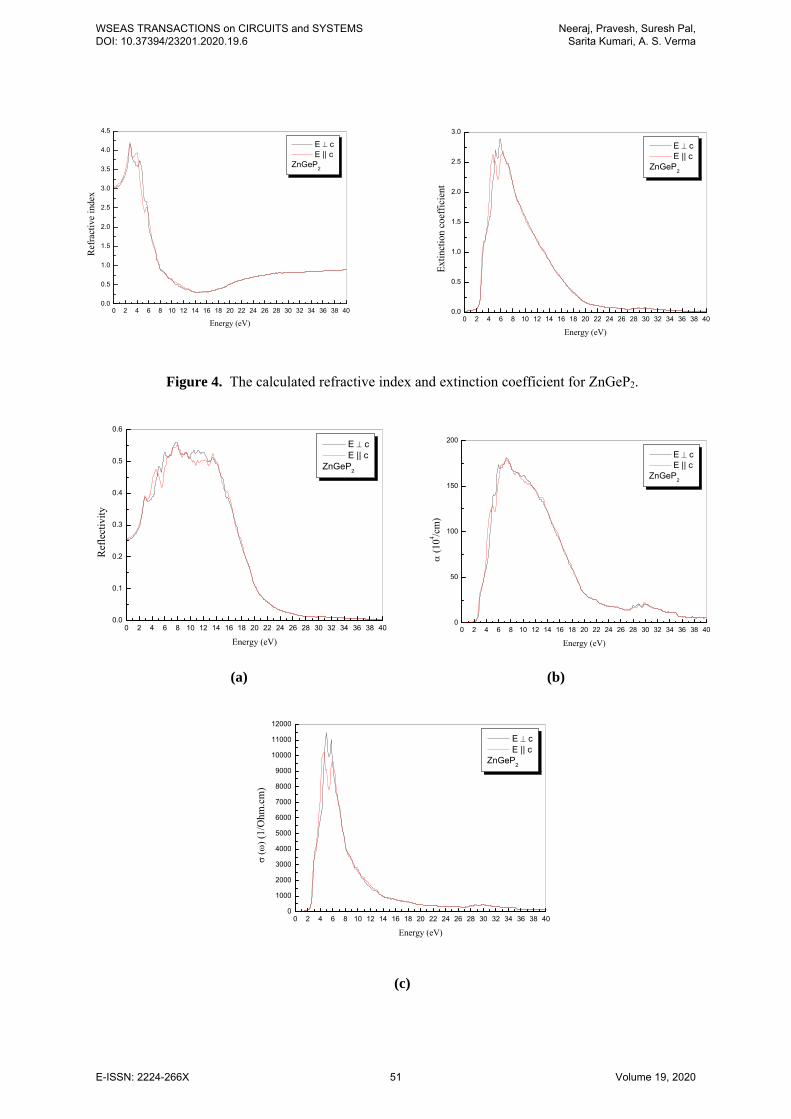
of the dielectric function ε2(ω) and shows that the critical points of the ε2 (ω) occurs at 2.0 eV. The obtained fundamental edges are closely related to the obtained energy band gap values 2.0 eV. The obtained values of band gap, refractive index and dielectric constant are presented in table 2 and compared with the available reported data. Figure 4 presents the refractive index n (ω) along with the extinction coefficient k (ω). The refractive index spectrum shows an anisotropic behavior (∆n (0 eV)=0.0334), hence only the average is listed in (3.04375) table 2. The peak value of refractive indices is 4.18 at 2.73 eV. Figure 4 also show extinction coefficient k (ω) is related to the decay or damping of the oscillation amplitude of the incident electric field, the extinction coefficient k (ω) decreases with increasing the incident photon energy. The calculated optical reflectivity R (ω) is displayed in Figure 5 (a) and this has small reflectivity in the low energy range. The maximum reflectivity occurs in region 4.22-14.67 eV [30]. The absorption coefficient is a parameter, which indicates the fraction of light lost by the electromagnetic wave, when it passes through a unit thickness of the material. These have been plotted in figure 5 (b). It is clear that polarization has a minor influence on the spectrum. From the absorption spectrum, we can easily find the absorption edges located at 1.99 eV. It is clear from the above discussion that both chalcopyrites are excellent mid-IR transparent crystal materials as they transparent to low energy photons showing zero value of the absorption coefficient in that region. When the photon energy is more than the absorption edge value, then adsorption coefficient increases. The absorption coefficients further decrease rapidly in the high energy region, which is the typical characteristic of semiconductors. Optical conductivity parameters are closely related to the photo-electric conversion efficiency and mainly used to measure the change caused by the illumination. Figure 5 (c) shows the optical conductivity and it’s clear that the maximum photoconductivity of the materials lies in the u-v region of electromagnetic spectrum. 3.2 Elastic Properties
The deformations [31] are shown in Table 3 and chosen such that the strained systems have the maximum possible symmetry. The elastic stiffness tensor of chalcopyrite compounds has six independent components because of the symmetry
WSEAS TRANSACTIONS on CIRCUITS and SYSTEMS DOI: 10.37394/23201.2020.19.6
Neeraj, Pravesh, Suresh Pal, Sarita Kumari, A. S. Verma
E-ISSN: 2224-266X 45 Volume 19, 2020

properties of the 122dD space group, namely C11, C12,
C13, C33, C44 and C66 in Young notation. The calculated elastic constant for the tetragonal phase of ZnGeP2 are listed in Table 4.
Voigt and Reuss approximations provides [32-35], in fact, an estimation of the elastic behaviour of an isotopic material, for instance a polycrystalline sample. We have found bulk (B in GPa) and shear modulus (G in GPa). Pugh [36] proposed that the resistance to plastic deformation is related to the product Gb, where ‘b’ is the Burgers vector, and that the fracture strength is proportional to the product Ba, where ‘a’ corresponds to the lattice parameter. As b and a are constants for specific materials, the Ba/Gb can be simplified into B/G. This formula was recently exploited in the study of brittle vs ductile transition in intermetallic compounds from first-principles calculations [37, 38]. A high B/G ratio is associated with ductility, whereas a low value corresponds to the brittle nature. The critical value which separates ductile and brittle material is around 1.75, i.e., if B/G > 1.75, the material behaves in a ductile manner otherwise the material behaves in a brittle manner. We have found that B/G ratios are 1.78 and classifying the materials is ductile.
3.3 Thermal Properties
To investigate the thermodynamic properties of Zn-chalcopyrite, we have used Gibbs program. The obtained set of total energy versus primitive cell volume determined in previous section has been used to derive the macroscopic properties as a function of temperature and pressure from the standard thermodynamic relations. Gibbs program is based on the quasi-harmonic Debye model [39], in which the non-equilibrium Gibbs function G*(V; P, T) can be written in the form of:
];[)(),;(* TAPVVETPVG Dvib (1)
where E(V) is the total energy per unit cell, PV corresponds to the constant hydrostatic pressure condition, θD is the Debye temperature, and Avib is the vibrational term, which can be written using the Debye model of the phonon density of states as [40, 41]:
TDe
TnkTTA T
Dvib
)1ln(38
9];[
(2)
where n is the number of atoms per formula unit, D (θ/T) represents the Debye integral, and for an isotropic solid, θ is expressed as [40]:
M
BfnV
kS
D 3
1
2126
(3)
M being the molecular mass per unit cell and BS the adiabatic bulk modulus, approximated by the static compressibility [39]:
2
2 )()(
dV
VEdVVBBS
(4)
f (σ) is given by Refs. [39, 42, 43]; where σ is the Poisson ratio.
Therefore, the non-equilibrium Gibbs function G*(V; P, T) as a function of (V; P, T) can be minimized with respect to volume V,
0),;(
,
TPV
TPVG (5)
By solving Eq. (17), one can obtain the thermal equation of state (EOS) V(P, T). The heat capacity CV and the thermal expansion coefficient α are given by [35],
1
343
TV e
T
TDnkC
(6)
)1ln(34 Te
TDnkS
(7)
VB
C
T
V (8)
where γ is the Grüneisen parameter, which is defined as:
Vd
Vd
ln
)(ln (9)
Through the quasi-harmonic Debye model, one could calculate the thermodynamic quantities of any temperatures and pressures of compounds from the calculated E–V data at T = 0 and P = 0. We can also provide a prediction of the hardness (H in GPa) by using the semi-empirical equations developed by Verma and co-authors [44],
H = K BK+1 (10)
WSEAS TRANSACTIONS on CIRCUITS and SYSTEMS DOI: 10.37394/23201.2020.19.6
Neeraj, Pravesh, Suresh Pal, Sarita Kumari, A. S. Verma
E-ISSN: 2224-266X 46 Volume 19, 2020
B = Bulk modulus; K = 0.59 for AIIBIVC2V
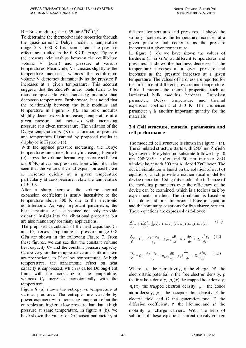
To determine the thermodynamic properties through the quasi-harmonic Debye model, a temperature range 0 K-1000 K has been taken. The pressure effects are studied in the 0–8 GPa range. Figure 6 (a) presents relationships between the equilibrium volume V (bohr3) and pressure at various temperatures. Meanwhile, V increases slightly as the temperature increases, whereas the equilibrium volume V decreases dramatically as the pressure P increases at a given temperature. This account suggests that the ZnGeP2 under loads turns to be more compressible with increasing pressure than decreases temperature. Furthermore, It is noted that the relationship between the bulk modulus and temperature in Figure 6 (b). The bulk modulus slightly decreases with increasing temperature at a given pressure and increases with increasing pressure at a given temperature. The variation of the Debye temperature D (K) as a function of pressure and temperature illustrated by proposed results is displayed in Figure 6 (d). With the applied pressure increasing, the Debye temperatures are almost linearly increasing. Figure 6 (e) shows the volume thermal expansion coefficient (10-5/K) at various pressures, from which it can be seen that the volume thermal expansion coefficient increases quickly at a given temperature particularly at zero pressure below the temperature of 300 K. After a sharp increase, the volume thermal expansion coefficient is nearly insensitive to the temperature above 300 K due to the electronic contributions. As very important parameters, the heat capacities of a substance not only provide essential insight into the vibrational properties but are also mandatory for many applications. The proposed calculation of the heat capacities CP and CV verses temperature at pressure range 0-8 GPa are shown in the following Figure 7. From these figures, we can see that the constant volume heat capacity CV and the constant pressure capacity CP are very similar in appearance and both of them are proportional to T3 at low temperatures. At high temperatures, the anharmonic effect on heat capacity is suppressed; which is called Dulong-Petit limit, with the increasing of the temperature, whereas CP increases monotonically with the temperature. Figure 8 (a) shows the entropy vs temperature at various pressures. The entropies are variable by power exponent with increasing temperature but the entropies are higher at low pressure than that at high pressure at same temperature. In figure 8 (b), we have shown the values of Grüneisen parameter at
different temperatures and pressures. It shows the value increases as the temperature increases at a given pressure and decreases as the pressure increases at a given temperature. In figure 8 (c), we have shown the values of hardness (H in GPa) at different temperatures and pressures. It shows the hardness decreases as the temperature increases at a given pressure and increases as the pressure increases at a given temperature. The values of hardness are reported for the first time at different pressure and temperature. Table 1 present the thermal properties such as isothermal bulk modulus, hardness, Grüneisen parameter, Debye temperature and thermal expansion coefficient at 300 K. The Grüneisen parameter is another important quantity for the materials. 3.4 Cell structure, material parameters and cell performance
The modeled cell structure is shown in Figure 9 (a). The simulated structure starts with 2500 nm ZnGeP2 layer over a Molybdenum substrate followed by 50 nm CdS/ZnSe buffer and 50 nm intrinsic ZnO window layer with 300 nm Al doped ZnO layer. The device simulation is based on the solution of a set of equations, which provide a mathematical model for device operation. Using this model, the influence of the modeling parameters over the efficiency of the device can be examined, which is a tedious task by experimental method. The simulation is based on the solution of one dimensional Poisson equation and the continuity equations for free charge carriers. These equations are expressed as follows:
xnxpxNxNxnxpqdx
dx
dx
dttAD
(11)
2
20
dx
pdD
dx
dpE
dx
dEp
ppG
dt
dp np
nppn
p
nnp
n
(12)
2
20
dx
ndD
dx
dnE
dx
dEn
nnG
dt
dn pn
p
nnpn
ppn
p
(13)
Where the permittivity, q the charge, the electrostatic potential, n the free electron density, p the free hole density, )(xpt the trapped hole density,
)(xnt the trapped electron density, DN the donor
atom density, AN the acceptor atom density, E the
electric field and G the generation rate, D the diffusion coefficient, the lifetime and the mobility of charge carriers. With the help of solution of these equations current density/voltage
WSEAS TRANSACTIONS on CIRCUITS and SYSTEMS DOI: 10.37394/23201.2020.19.6
Neeraj, Pravesh, Suresh Pal, Sarita Kumari, A. S. Verma
E-ISSN: 2224-266X 47 Volume 19, 2020

(J/V) characteristics are determined and performance of solar cell with different buffer layers is compared. In Table 5 we have presented description for the parameters; which was used in the simulation. The terrestrial spectrum AM 1.5 (Air Mass 1.5 Global 1000W/m2) is used for illumination. The schematic energy band diagram under equilibrium condition for the thin layer solar cell has been illustrated in Figure 9 (b). The band diagram is drawn according to Anderson’s affinity rule, which shows conduction band offset is ∆Ec = 2 1 and valance band offset is ∆Ec = (1 + Eg1) (2 + Eg2). The band diagram shows that this is a type II heterostructure. The difference in band gaps creates discontinuity spikes in the conduction- and valence bands. These spikes can create extra barriers for the electrons to overcome or tunnel through, and may also work as potential wells with discrete energy states [52]. The Figure 9 (c) shows the illuminated characteristics J-V curve of the proposed solar cell structures. The performance parameters open circuit voltage (Voc), short circuit current density (Jsc), Fill Factor (FF) and efficiency () have been calculated from J-V characteristics for different considered buffer layers. The simulation results have been presented in Table 6 (a) and 6 (b). These results show that both the buffer layers provide good efficiency (>20%). A maximum density of current (>29 mA/cm2) has been obtained with both the buffer layers, which ensures the suitability of CdS and ZnSe buffer layers in ZnGeP2 solar cells.Further, the analysis of photoconductivity of cell structure is done in terms of quantum efficiency (QE) as shown in figure 9 (d). The spectral response of the device is studied within the spectral range of 0.4 m to 1.0 m. Quantum efficiency is a measure of collection of charge carriers with respect to number of incident photons. As CdS buffer layer has higher band gap, it provides a wider window for absorption of photons, thus creating larger number of charge carriers and resulting in higher quantum efficiency in lower wavelength region, whereas in higher wavelength region QE of CdS becomes lower which ensures higher recombination in this structure. The higher values of quantum efficiencies are found for blue region of the light. Since blue light is absorbed closer to the junction, recombination effect is less effective for this wavelength region whereas at higher side of wavelength high recombination occurs, since the free carrier generated deeper in the bulk have to travel longer before being collected. This results higher recombination loss and in tern lower quantum efficiency in long wavelength region. Moreover, the absorption coefficient
decreases with the increasing of the photon wavelength, so the loss in absorption causes the spectral response to decrease quickly and thus the quantum efficiency.
3.5 Effect of buffer layer thickness
The effect of thickness of buffer layer on J-V characteristics for the two cell structures are shown in figures 9 (e)-9 (f). With the help of these
characteristics scJ , ocV , η and FF are calculated at different thickness of buffer layers. The effect of thickness of buffer layer over performance parameters of these cell structures is shown in figures 10 (a)-10 (c). Figure 10 (a) and 10 (b) shows that as thickness of buffer layer increases, the current density as well as efficiency start to decrease for both the structures. This shows that at 50 nm the ratio of diffusion length to the thickness of the buffer layer is appropriate for collection of minority carriers. After this thickness all the photogenerated carriers are not able to reach the depletion region, which in turn decreases the current density and efficiency. The decrement in current density at lower thickness values is fast in ZnGeP2/ZnSe structure, which shows that rate of recombination is higher in ZnGeP2/ZnSe solar cell structure. Effect of thickness over fill factor for the two structures is shown in figure 10 (c). It is a measure of maximum power that can be achieved by a cell. As both the structures are showing the highest FF at 50nm thickness, ensures that at lower values of thickness charge collection is good because charge carriers are able to reach the electrodes. After this thickness charge collection suffers due to low values of diffusion length than the thickness of buffer layer. Further, with increment in thickness FF becomes almost constant because maximum effect of recombination over charge collection is achieved. 3.6 Effect of temperature
The effect of temperature over J-V characteristics for both the three structures is shown in Figure 10 (d) and 10 (e). Further, figures 10 (f)-11(e) show the effect of temperature over performance parameters for the two cell structures. In fig 10 (f), Jsc increases with temperature for both the structures considered. This effect can be understood in terms of band gap. The effect of temperature over energy band gap, Eg is given by Varshni equation [53]
T
TETE gg
2
)0()( (14)
WSEAS TRANSACTIONS on CIRCUITS and SYSTEMS DOI: 10.37394/23201.2020.19.6
Neeraj, Pravesh, Suresh Pal, Sarita Kumari, A. S. Verma
E-ISSN: 2224-266X 48 Volume 19, 2020

Where Eg (0) is the band gap energy at absolute zero on the Kelvin scale in the given material, and and are material-specific constants. This decrement in band gap is responsible for enhancement in current density values at higher temperature. Increase in temperature can be viewed as increase the energy of the charge carriers. Thus less energy is required to break the bond and conduction increases. As a consequence of the increase in temperature, there is a shift in quantum efficiency curves (figure 11 (a),11 (b). When the temperature of the cell is increased, thermal vibrations of the lattice becomes stronger, which causes reduction in lifetime and mobility of minority charge carriers. This in turn reduces the diffusion length and process of recombination becomes stronger. But with increase in temperature, the band gap is reduced, which enhances the production of charge carriers. In low and middle temperature range, there is equilibrium in between the phenomenon of charge generation and recombination. But with temperature, the absorption in wide band gap materials is improved for long wavelength region because of the phonons multiplication phenomenon [54]. So, the minority carriers production is increased with temperature in the range of long wavelengths, thus the photocurrent increases and consequently, the quantum efficiency. Further with temperature a sharp increment is found in ocV (figure 11 (c)). The effect over ocV can be understood as a measure of the amount of recombination in the device. As the temperature increases, the number of thermally generated carriers can exceed the number of dopant-generated carriers. Though the concentration of intrinsic carriers is very small; but it has very strong temperature dependence [55]. This increment in intrinsic carrier concentration causes the increase in reverse saturation current. The increment in reverse saturation current is responsible for decrement in open circuit voltage values. Also, the temperature dependence of ocV is given by [56]
T
qEV
dT
qdE
dT
dV gocgoc //
(15)
From eq. (15) it is inferred that the temperature
dependence is mainly related to the termT
qEV goc / ;
which after integration provides a linear relationship TcVo as observed experimentally [56].
Therefore, the tendency of Voc to decrease and Jsc to increase with increasing temperature in the solar cells are determining factor for efficiency with
variation in temperature. The overall effect of temperature has been studied for as shown in figure 11 (d).
3.7 Effect of Band gap of absorption layer
The effect of band gap of absorption layer over performance parameters is studied. To find the effect of band gap, the results of ZnGeP2 absorption layer with band gap 2.0 eV and 2.3 eV are compared. The effect of band gap of absorption layer over J-V characteristics of the cell are shown in figure 11 (f)-11 (g). These results show that the increment in band gap results in an increment in absorption of light, thus an increment in performance parameters is found (Table 6a and 6b). This improvement in parameters is due to the enhancement of absorption in longer wavelength region. This effect can be seen in quantum efficiency curves in figure 11 (f) and 11 (g). Hence, the study shows that ZnGeP2 as absorption layer with CdS and ZnSe buffer can be promising solar cell model. ZnSe can be used as an option for CdS buffer layer, which is not only beneficial on the energy basis, but also helps in overcoming the serious environmental related problems due to the toxic nature of cadmium.
4 Conclusion To conclude, results have been presented for the solid state properties such as structural, electronic, optical, elastic and thermal properties of the ZnGeP2 semiconductor using the first-principles calculation. The structural properties in the chalcopyrite structure are obtained using the total energy as a function of volume; the derived equilibrium parameters are compared with experimental data. We compared electronic and optical properties calculated with the mBJ functional and spectroscopic ellipsometry data. We find that the mBJ functional provides an accurate description of the electronic and optical properties. The ZnGeP2 has a direct band gap. We have also derived the static refractive index. Thermal properties such as Gruneisen parameter, volume expansion coefficient, bulk modulus, specific heat, entropy, debye temperature and hardness are calculated successfully at various temperatures and pressures, and trends are discussed. The ground state parameters of interest were obtained and showed good agreement with published experimental and theoretical data. An application of the material in solar cell device has been presented; here we have used AMPS-1D to investigate the dependence of the
WSEAS TRANSACTIONS on CIRCUITS and SYSTEMS DOI: 10.37394/23201.2020.19.6
Neeraj, Pravesh, Suresh Pal, Sarita Kumari, A. S. Verma
E-ISSN: 2224-266X 49 Volume 19, 2020

buffer layer for thin layer ZnGeP2 solar cells. A device modelling and detailed simulation study have been carried out over single junction ZnGeP2 solar cell with a variety of buffer layers. The performance parameters of solar cells as open-circuit voltage (Voc), the short-circuit current density (Jsc), the conversion efficiency η, Fill factor (FF) and quantum efficiency (QE) have been calculated. Also the effect of temperature and band gap of absorption
layer is studied and it is found that higher band gap of absorption layer improves the performance of solar cell. Thus the study shows that ZnSe can be considered as an alternative to CdS buffer layer and assumes greater significance under this scenario. To the best of our knowledge, most of the investigated parameters are reported for the first time and will further stimulate the research in the related field.
950 1000 1050 1100 1150 1200-18312.26
-18312.25
-18312.24
-18312.23
-18312.22
-18312.21
Ene
rgy
(Ry)
V (bohr3)
Figure 1. Calculated total energies as a function of volume
Figure 2. Band structures of ZnGeP2
0 2 4 6 8 10 12 14 16 18 20 22 24 26 28 30 32 34 36 38 40
-4
-2
0
2
4
6
8
10
12
14
16
18
20
1
Energy (eV)
E c E || c
ZnGeP2
0 2 4 6 8 10 12 14 16 18 20 22 24 26 28 30 32 34 36 38 400
2
4
6
8
10
12
14
16
18
20
2
Energy (eV)
E c E || c
ZnGeP2
(a) (b)
Figure 3. The calculated (a) real ε1(ω) and (b) imaginary ε2(ω) parts of complex dielectric constant for ZnGeP2.
WSEAS TRANSACTIONS on CIRCUITS and SYSTEMS DOI: 10.37394/23201.2020.19.6
Neeraj, Pravesh, Suresh Pal, Sarita Kumari, A. S. Verma
E-ISSN: 2224-266X 50 Volume 19, 2020
0 2 4 6 8 10 12 14 16 18 20 22 24 26 28 30 32 34 36 38 400.0
0.5
1.0
1.5
2.0
2.5
3.0
3.5
4.0
4.5
Ref
ract
ive
inde
x
Energy (eV)
E c E || c
ZnGeP2
0 2 4 6 8 10 12 14 16 18 20 22 24 26 28 30 32 34 36 38 400.0
0.5
1.0
1.5
2.0
2.5
3.0
Ext
inct
ion
coef
fici
ent
Energy (eV)
E c E || c
ZnGeP2
Figure 4. The calculated refractive index and extinction coefficient for ZnGeP2.
0 2 4 6 8 10 12 14 16 18 20 22 24 26 28 30 32 34 36 38 400.0
0.1
0.2
0.3
0.4
0.5
0.6
Ref
lect
ivity
Energy (eV)
E c E || c
ZnGeP2
0 2 4 6 8 10 12 14 16 18 20 22 24 26 28 30 32 34 36 38 400
50
100
150
200
(10
4 /cm
)
Energy (eV)
E c E || c
ZnGeP2
(a) (b)
0 2 4 6 8 10 12 14 16 18 20 22 24 26 28 30 32 34 36 38 400
1000
2000
3000
4000
5000
6000
7000
8000
9000
10000
11000
12000
(
1/O
hm.c
m)
Energy (eV)
E c E || c
ZnGeP2
(c)
WSEAS TRANSACTIONS on CIRCUITS and SYSTEMS DOI: 10.37394/23201.2020.19.6
Neeraj, Pravesh, Suresh Pal, Sarita Kumari, A. S. Verma
E-ISSN: 2224-266X 51 Volume 19, 2020

Figure 5. (a) The calculated reflectivity (R ()), (b) absorption coefficient (()) and (c) photoconductivity (()) for ZnGeP2.
0 100 200 300 400 500 600 700 800 900 1000
1000
1020
1040
1060
1080
1100
1120
V (
bohr
3 )
Temperature (K)
0 GPa 2 GPa 4 GPa 6 GPa 8 GPa
0 100 200 300 400 500 600 700 800 900 1000
70
80
90
100
110
B (
GPa
)
Temperature (K)
0 GPa 2 GPa 4 GPa 6 GPa 8 GPa
Figure 6. (a) Volume vs temperature at various pressures.
Figure 6. (b) Bulk modulus vs temperature at various pressures.
0 1 2 3 4 5 6 7 8380
390
400
410
420
430
440
450
460
470
480
490
D (
K)
Pressure (GPa)
0 K 100 K 200 K 300 K 400 K 500 K 600 K 700 K 800 K 900 K 1000 K
0 100 200 300 400 500 600 700 800 900 10000
1
2
3
4
5
6
(10
-5/K
)
Temperature (K)
0 GPa 2 GPa 4 GPa 6 GPa 8 GPa
Figure 6. (d) Debye temperature vs pressure at various temperatures.
Figure 6. (e) Thermal expansion coefficients vs temperature at various pressures.
0 100 200 300 400 500 600 700 800 900 10000
50
100
150
200
250
CP (
J/m
ol.K
)
Temperature (K)
0 GPa 2 GPa 4 GPa 6 GPa 8 GPa
0 100 200 300 400 500 600 700 800 900 10000
50
100
150
200
CP (
J/m
ol.K
)
Temperature (K)
0 GPa 2 GPa 4 GPa 6 GPa 8 GPa
WSEAS TRANSACTIONS on CIRCUITS and SYSTEMS DOI: 10.37394/23201.2020.19.6
Neeraj, Pravesh, Suresh Pal, Sarita Kumari, A. S. Verma
E-ISSN: 2224-266X 52 Volume 19, 2020

Figure 7. Heat capacity vs temperature at various pressures for ZnGeP2.
0 100 200 300 400 500 600 700 800 900 10000
50
100
150
200
250
300
350
400
450
500
S (J
/mol
.K)
Temperature (K)
0 GPa 2 GPa 4 GPa 6 GPa 8 GPa
0 100 200 300 400 500 600 700 800 900 10001.70
1.75
1.80
1.85
1.90
1.95
Temperature (K)
0 GPa 2 GPa 4 GPa 6 GPa 8 GPa
Figure 8. (a) Entropy vs temperature Figure 8. (b) Gruneisen parameter vs temperature
0 100 200 300 400 500 600 700 800 900 1000
5.0
5.5
6.0
6.5
7.0
7.5
8.0
8.5
9.0
9.5
10.0
10.5
11.0
Har
dnes
s (H
in G
Pa)
Temperature (K)
0 GPa 2 GPa 4 GPa 6 GPa 8 GPa
Figure 8. (c) Hardness vs temperature at various pressures
Figure 9 (a): The layer structure of ZnGeP2 solar cell . Figure 9 (b): The schematic energy-band diagram of a typical ZnGeP2 /CdS or ZnSe solar cell under thermal
WSEAS TRANSACTIONS on CIRCUITS and SYSTEMS DOI: 10.37394/23201.2020.19.6
Neeraj, Pravesh, Suresh Pal, Sarita Kumari, A. S. Verma
E-ISSN: 2224-266X 53 Volume 19, 2020

equilibrium condition.
Figure 9 (c): Photo-current density-voltage (J-V) curves for the simulated results for 50nm thickness of CdS and ZnSe buffer layers.
Figure 9 (d): Quantum efficiency curves for ZnGeP2/CdS or ZnSe solar cell for 50 nm thickness of buffer layer.
Figure 9 (e): Effect of thickness of buffer layer over J–V characteristics of ZnGeP2/CdS solar cell.
Figure 9 (f): Effect of thickness of buffer layer over J–V characteristics of ZnGeP2/ZnSe solar cell.
Figure 10 (a): Effect of thickness of buffer layer over current density of ZnGeP2 solar cell with CdS/ZnSe buffer layer.
Figure 10 (b): Effect of thickness of buffer layer over efficiency of ZnGeP2 solar cell with CdS/ZnSe buffer layer.
WSEAS TRANSACTIONS on CIRCUITS and SYSTEMS DOI: 10.37394/23201.2020.19.6
Neeraj, Pravesh, Suresh Pal, Sarita Kumari, A. S. Verma
E-ISSN: 2224-266X 54 Volume 19, 2020

Figure 10 (c): Effect of thickness of buffer layer over fill factor of ZnGeP2 solar cell with CdS/ZnSe buffer layer.
Figure 10 (d): Effect of temperature over J-V characteristics of ZnGeP2/ZnSe solar cell.
Figure 10 (e): Effect of temperature over J-V characteristics of ZnGeP2/CdS solar cell.
Figure 10 (f): Effect of temperature over current density of ZnGeP2/CdS or ZnSe solar cell structures.
Figure 11 (a): Effect of temperature over quantum efficiency of ZnGeP2/CdS solar cell
Figure 11 (b): Effect of temperature over quantum efficiency of ZnGeP2/ZnSe solar cell.
WSEAS TRANSACTIONS on CIRCUITS and SYSTEMS DOI: 10.37394/23201.2020.19.6
Neeraj, Pravesh, Suresh Pal, Sarita Kumari, A. S. Verma
E-ISSN: 2224-266X 55 Volume 19, 2020
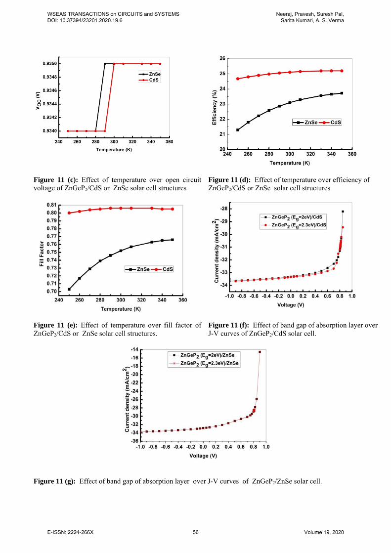
Figure 11 (c): Effect of temperature over open circuit voltage of ZnGeP2/CdS or ZnSe solar cell structures
Figure 11 (d): Effect of temperature over efficiency of ZnGeP2/CdS or ZnSe solar cell structures
Figure 11 (e): Effect of temperature over fill factor of ZnGeP2/CdS or ZnSe solar cell structures.
Figure 11 (f): Effect of band gap of absorption layer over J-V curves of ZnGeP2/CdS solar cell.
Figure 11 (g): Effect of band gap of absorption layer over J-V curves of ZnGeP2/ZnSe solar cell.
WSEAS TRANSACTIONS on CIRCUITS and SYSTEMS DOI: 10.37394/23201.2020.19.6
Neeraj, Pravesh, Suresh Pal, Sarita Kumari, A. S. Verma
E-ISSN: 2224-266X 56 Volume 19, 2020

Table 1. Structural equilibrium parameters, a, c, u, B and B calculated in WC-GGA and thermal properties at 300 K; isothermal bulk modulus (B in GPa), Hardness (H in GPa), Gruneisen parameter (), Debye temperature (D in K) and thermal expansion coefficient ( in 10−5/K) of ZnGeP2.
Structural Analysis
a (Å) c (Å) u B (GPa) B
5.43, 5.46a,*
10.73, 10.71a, *
0.255 84 4.58
Thermal Analysis
B (GPa) H (GPa) D (K) (10-
5/K)
80 6.19, 6.2b 1.864 414, 410c 4.345
a Reference [45]; *Experimental; b Reference [50]; c Reference [51];
Table 2. The calculated minimum band gaps Eg (eV), refractive index (n) and dielectric constant for ZnGeP2 compared with other experimental and theoretical data.
Crystals Eg (eV) this work
n this work this work
ZnGeP2 2.0, 2.0-2.3d,*, 1.98e
3.04, 3.10f,* 9.26, 9.18g
d Reference [24]; e Reference [46]; f Reference [47]; g Reference [48]; *Experimental
Table 3. The lattice parameters of the deformed tetragonal unit cell, the expression relating the and variables, the finite Lagrangian strain tensor (Voigt notation) and the value of the second derivative, (1/2V)(d2E/d2), in terms of the elastic constants ( being deformation coordinate and E the energy).
Strained cell ε Strain (η) dE2/d ε2
90,90,90,,,(a
ccaa
)90,90,90,,,( caa
)90,90,90,,,(a
ccaa
)90,90,90,,,( caa
)90,90,90,,,( caa
)90,90,90,,,( caa
1)(
2
2
a
a
1)(
2
2
a
a
1)(
2
2
c
c
1)(
2
2
a
a
sin
sin
)0,0,0,2
,2
,2
(a
c
)0,0,0,0,2
,2
(
)0,0,0,2
,0,0(
)0,0,0,0,2
,0(
)0,,0,0,0,0(
),0,0,0,0,0(
331211 8
1)(
4
1CCC
)(4
11211 CC
338
1C
118
1C
44C
66C
Table 4. Elastic constants Cij (in GPa) of the ZnGeP2 compared with available data.
C11 C12 C13 C33 C44 C66
133, 88h 65, 55 h 66, 52 h 134, 82 h 64, 30 h 64, 27 h
B (GPa) G (GPa) Y (GPa) a (GPa-1) c (GPa-1)
88 50 126 0.26 0.0038 0.0037
h Reference [49];
WSEAS TRANSACTIONS on CIRCUITS and SYSTEMS DOI: 10.37394/23201.2020.19.6
Neeraj, Pravesh, Suresh Pal, Sarita Kumari, A. S. Verma
E-ISSN: 2224-266X 57 Volume 19, 2020

Table 5: Material properties for the ZnGeP2 solar cells simulation.
Layers
Parameters
1-n+ZnO 2-n(i) ZnO 3-CdS 3-ZnSe 4-ZnGeP2
Thickness (nm) 300 50 50a 50 2500
(dielectric constant) 9.26 b 9 c 9.4b 10c 9.26d
n (electron mobility in 10cm2/Vs) 65.6 e 230 f 265 g 50 c l000h
p (hole mobility in 10cm2/Vs) 65 i 70 j 15 g 20 c 40k
n/p (carrier density in cm-3) 1.71019l 51016l 61016l 11017m 1012k
Eg (eV) (optical band gap) 3.228n 3.29 n 2.42 m 2.9 c 2d
Nc (electron density in cm-3) 11019l 11019l 11019l 1.51018 c 6.8x10¹⁷
Nv (effective density in cm-3) 11019l 11019l 1.61019l 1.81019 a 1.5x 10¹⁹
electron affinity (eV) 3.9l 3.9l 3.75 l 4.09c 3.58o
a Reference [57]; b Reference [58]; c Reference [59]; d This work; e Reference [60]; f Reference [61] ; g Reference[62], hReference[63], iReference [64], j
Reference[65], kReference[66], lReference[67], mReference[68], nReference[69]; oReference[70]
Table 6 (a): Simulated performance parameters of the solar cells for absorption layer ZnGeP2 (Eg= 2eV)
Buffer layer (%) Voc(mV) Jsc(mA/cm2) FF(%)
ZnSe 21.139 0.934 29.456 0.768
CdS 22.518 0.934 30.666 0.786
Table 6 (b): Simulated performance parameters of the solar cells for absorption layer ZnGeP2 (Eg= 2.3eV)
Buffer layer (%) Voc(mV) Jsc(mA/cm2) FF(%)
ZnSe 23.097 0.935 32.849 0.752
CdS 23.840 0.931 33.326 0.769
WSEAS TRANSACTIONS on CIRCUITS and SYSTEMS DOI: 10.37394/23201.2020.19.6
Neeraj, Pravesh, Suresh Pal, Sarita Kumari, A. S. Verma
E-ISSN: 2224-266X 58 Volume 19, 2020

References: [1] Mukherjee, S., T. Maitra, A. Nayak, A. Pradhan, M. K.
Mukhopadhyay, B. Satpati, and S. Bhunia. "Microstructural and light emission properties of ZnSnP2 thin film absorber: Study of native defects" Materials Chemistry and Physics 204 (2018) 147-153.
[2] Sharma, Sheetal, and Ajay Singh Verma. "Structural, electronic, optical, elastic and thermal properties of ZnXAs2 (X= Si and Ge) chalcopyrite semiconductors" The European Physical Journal B 87 (2014) 159.
[3] Sahin, S., Y. O. Ciftci, K. Colakoglu, and N. Korozlu. "First principles studies of elastic, electronic and optical properties of chalcopyrite semiconductor ZnSnP2" Journal of Alloys and Compounds 529 (2012) 1-7.
[4] Martinez, Aaron D., Emily L. Warren, Prashun Gorai, Kasper A. Borup, Darius Kuciauskas, Patricia C. Dippo, Brenden R. Ortiz et al. "Solar energy conversion properties and defect physics of ZnSiP2" Energy & Environmental Science 9 (2016) 1031-1041.
[5] Martinez, Aaron D., Angela N. Fioretti, Eric S. Toberer, and Adele C. Tamboli. "Synthesis, structure, and optoelectronic properties of II–IV–V2 materials" J. Materials Chemistry A 5 (2017) 11418-11435.
[6] Miyauchi, Keisuke, Takehiro Minemura, Keigo Nakatani, Hisayuki Nakanishi, Mutsumi Sugiyama, and Sho Shirakata. "Photoluminescence properties of ZnSnP2 single crystals" Physica Status Solidi C 6 (2009) 1116-1119.
[7] Nakatsuka, Shigeru, Shunsuke Akari, Jakapan Chantana, Takashi Minemoto, and Yoshitaro Nose. "Impact of Heterointerfaces in Solar Cells Using ZnSnP2 Bulk Crystals" ACS applied materials & interfaces 9 (2017) 33827-33832.
[8] Nakatsuka, Shigeru, Noriyuki Yuzawa, Jakapan Chantana, Takashi Minemoto, and Yoshitaro Nose "Solar cells using bulk crystals of rare metal‐free compound semiconductor ZnSnP2" Physica Status Solidi A 214 (2017) 1600650.
[9] Scanlon, David O., and Aron Walsh. "Band gap engineering of ZnSnP2 for high-efficiency solar cells" Applied Physics Letters 100 (2012) 251911.
[10] Sreeparvathy, P. C., V. Kanchana, and G. Vaitheeswaran. "Thermoelectric properties of zinc based pnictide semiconductors" J. Applied Physics 119 (2016) 085701.
[11] Verma, A. S. "Bulk modulus and hardness of chalcopyrite structured solids" Materials Chemistry and Physics 139 (2013) 256-261.
[12] Yuzawa, Noriyuki, Jakapan Chantana, Shigeru Nakatsuka, Yoshitaro Nose, and Takashi Minemoto. "ZnSnP2 thin-film solar cell prepared by phosphidation method under optimized Zn/Sn atomic ratio of its absorbing layer" Current Applied Physics 17 (2017) 557-564.
[13] Zhang, Yujun. "Bandgap nature of chalcopyrite ZnXP2 (X= Si, Ge, Sn)" Computational Materials Science 133 (2017): 152-158.
[14] Madsen, Georg KH, Peter Blaha, Karlheinz Schwarz, Elisabeth Sjöstedt, and Lars Nordström. "Efficient linearization of the augmented plane-wave method" Physical Review B 64 (2001) 195134.
[15] Schwarz, Karlheinz, Peter Blaha, and Georg KH Madsen. "Electronic structure calculations of solids using the WIEN2k package for material sciences" Computer Physics Communications 147 (2002) 71-76.
[16] P. Blaha, K. Schwarz, G. K. H. Madsen, D. Kvasnicka, and J. Luitz, WIEN2k: An Augmented Plane Wave+Local Orbitals Program for Calculating Crystal Properties (Karlheinz Schwarz/Techn. Universität Wien, Austria, 2001).
[17] Wu, Zhigang, and Ronald E. Cohen. "More accurate generalized gradient approximation for solids" Physical Review B 73 (2006) 235116.
[18] Tran, Fabien, Robert Laskowski, Peter Blaha, and Karlheinz Schwarz. "Performance on molecules, surfaces, and solids of the Wu-Cohen GGA exchange-correlation energy functional" Physical review B 75 (2007) 115131.
[19] Sham, Lu J., and Michael Schlüter. "Density-functional theory of the energy gap" Physical Review Letters 51 (1983) 1888.
[20] Perdew, J. P., K. Burke, and M. Ernzerhof. "Perdew, burke, and ernzerhof reply" Physical Review Letters 80 (1998) 891.
[21] Tran, Fabien, and Peter Blaha. "Accurate band gaps of semiconductors and insulators with a semilocal exchange-correlation potential" Physical Review Letters 102 (2009) 226401.
WSEAS TRANSACTIONS on CIRCUITS and SYSTEMS DOI: 10.37394/23201.2020.19.6
Neeraj, Pravesh, Suresh Pal, Sarita Kumari, A. S. Verma
E-ISSN: 2224-266X 59 Volume 19, 2020

[22] Blöchl, Peter E., Ove Jepsen, and Ole Krogh Andersen. "Improved tetrahedron method for Brillouin-zone integrations" Physical Review B 49 (1994) 16223.
[23] Murnaghan, F. D. "The compressibility of media under extreme pressures" Proceedings of the national academy of sciences of the United States of America 30 (1944) 244.
[24] Shaposhnikov, V. L., A. V. Krivosheeva, V. E. Borisenko, J-L. Lazzari, and F. Arnaud d’Avitaya. "Ab initio modeling of the structural, electronic, and optical properties of AIIBIVC2V semiconductors" Physical Review B 85 (2012) 205201.
[25] Sun, Jian, Hui-Tian Wang, Nai-Ben Ming, Julong He, and Yongjun Tian. "Optical properties of heterodiamond B2CN using first-principles calculations" Applied Physics Letters 84 (2004) 4544-4546.
[26] Saha, Sonali, T. P. Sinha, and Abhijit Mookerjee. "Electronic structure, chemical bonding, and optical properties of paraelectric BaTiO3" Physical Review B 62 (2000) 8828.
[27] P. Y. Yu and M. Cardona, Fundamentals of Semiconductors, (Springer-Verlag, Berlin, 1996)
[28] Cai, Meng-Qiu, Zhen Yin, and Ming-Sheng Zhang. "First-principles study of optical properties of barium titanate" Applied Physics Letters 83 (2003) 2805-2807.
[29] Verma, A. S. "Correlation between ionic charge and the optical properties of zinc blende and complex crystal structured solids" Physica Status Solidi (b) 246 (2009) 192-199.
[30] Rife, J. C., R. N. Dexter, P. M. Bridenbaugh, and B. W. Veal. "Optical properties of the chalcopyrite semiconductors ZnGeP2, ZnGeAs2, CuGaS2, CuAlS2, CuInSe2, and AgInSe2" Physical Review B 16 (1977) 4491.
[31] J. F. Nye, Physical Properties of Crystals, Their Representation by Tensors and Matrices, Oxford Univ. Press, Oxford, USA, 1985
[32] W. Voigt, Lehrbuch der Kristallphysik, Teubner, Leipzig, 1928 [33] Shein, I. R., and A. L. Ivanovskii. "Elastic properties of quaternary
oxypnictides LaOFeAs and LaOFeP as basic phases for new 26–52 K superconducting materials from first principles." Scripta Materialia 59 (2008) 1099-1102.
[34] Reuss, A. "Mittelung von Fließgrenze und elastischen Eigenschaften" Z. angew. Math. Mech. Bd 9 (1929) 49.
[35] Hill, Richard. "The elastic behaviour of a crystalline aggregate" Proceedings of the Physical Society. Section A 65 (1952) 349.
[36] Pugh, S. F. "XCII. Relations between the elastic moduli and the plastic properties of polycrystalline pure metals" The London, Edinburgh, and Dublin Philosophical Magazine and Journal of Science 45 (1954): 823-843.
[37] Chen, Kuiying, L. R. Zhao, and John S. Tse. "Ab initio study of elastic properties of Ir and Ir3X compounds" J Applied Physics 93 (2003) 2414-2417.
[38] Chen, K., L. R. Zhao, J. S. Tse, and J. R. Rodgers. "Elastic properties of platinum Rh and Rh3X compounds" Physics Letters A 331 (2004) 400-403.
[39] Blanco, M. A., E. Francisco, and V. Luana. "GIBBS: isothermal-isobaric thermodynamics of solids from energy curves using a quasi-harmonic Debye model" Computer Physics Communications 158 (2004) 57-72.
[40] Blanco, M. A., A. Martín Pendás, E. Francisco, J. M. Recio, and R. Franco. "Thermodynamical properties of solids from microscopic theory: applications to MgF2 and Al2O3" J. Molecular Structure: THEOCHEM 368 (1996) 245-255.
[41] Flórez, M., J. M. Recio, E. Francisco, M. A. Blanco, and A. Martín Pendás. "First-principles study of the rocksalt–cesium chloride relative phase stability in alkali halides" Physical Review B 66 (2002) 144112.
[42] Francisco, E., M. A. Blanco, and G. Sanjurjo. "Atomistic simulation of Sr F 2 polymorphs" Physical Review B 63 (2001) 094107.
[43] J. P. Poirier, Introduction to the Physics of Earth’s Interior, Cambridge University Press, Oxford, 2000, p. 39
[44] Verma, A. S., and S. R. Bhardwaj. "Correlation between ionic charge and the mechanical properties of complex structured solids" J. Physics: Condensed Matter 19 (2006) 026213.
[45] Kimmel, G., Y. Shimony, O. Raz, and M. P. Dariel. "Order and Disorder in ZnGeP2 Crystals" Materials Structure 6 (1999) 149.
[46] Verma, Ajay Singh, Sheetal Sharma, and V. K. Jindal. "Evaluating optical parameters from electronic structure and crystal structure for binary (anb 8-n) and ternary tetrahedral semiconductors" Modern Physics Letters B 24 (2010) 2511-2524.
WSEAS TRANSACTIONS on CIRCUITS and SYSTEMS DOI: 10.37394/23201.2020.19.6
Neeraj, Pravesh, Suresh Pal, Sarita Kumari, A. S. Verma
E-ISSN: 2224-266X 60 Volume 19, 2020

[47] Verma, A. S. "Correlation between ionic charge and the optical properties of zinc blende and complex crystal structured solids" Physica Status Solidi B 246 (2009) 192-199.
[48] Verma, A. S., and D. Sharma. "Dielectric constants of AIBIIIC2VI and AIIBIVC2V chalcopyrite semiconductors" Physica Scripta 76 (2007) 22.
[49] Verma, A. S., Sheetal Sharma, R. Bhandari, B. K. Sarkar, and V. K. Jindal. "Elastic properties of chalcopyrite structured solids" Materials Chemistry and Physics 132 (2012) 416-420.
[50] Verma, A. S. "Bulk modulus and hardness of chalcopyrite structured solids" Materials Chemistry and Physics 139 (2013) 256-261.
[51] Kumar, V., A. K. Shrivastava, Rajib Banerji, and D. Dhirhe. "Debye temperature and melting point of ternary chalcopyrite semiconductors" Solid State Communications 149 (2009) 1008-1011.
[52] B. G. Streetman, S. K. Banerjee, Solid State Electronic Devices' 6th ed. Pearson int. ed., (2010)
[53] Varshni, Yatendra Pal. "Temperature dependence of the energy gap in semiconductors" Physica 34 (1967) 149-154.
[54] B. O. Seraphin, Solar Energy Conversion–Solid State Physics Aspects Topics in Applied Physics, Volume 31, Springer, (1979)
[55] S. M. Sze, Physics of semiconductor devices, 2nd ed. John Wiley and Sons, NY (1981).
[56] P. Wurfel, Physics of Solar Cells, Wiley-VCH Verlag, Weinheim, 2005
[57] M. A. Green, Solar Cells, Operating Principles, Technology and System Applications, Prentice Hall Inc., (1982)
[58] Young, K. F., and H. P. R. Frederikse. "Compilation of the static dielectric constant of inorganic solids" Journal of Physical and Chemical Reference Data 2 (1973): 313-410.
[59] Olopade, M. A., O. O. Oyebola, and B. S. Adeleke. "Investigation of some materials as buffer layer in copper zinc tin sulphide (Cu2ZnSnS4) solar cells by SCAPS-1D" Advances in Applied Science Research 3 (2012) 3396-3400.
[60] Kim, Kyoung-Kook, Shigeru Niki, Jin-Yong Oh, June-O. Song, Tae-Yeon Seong, Seong-Ju Park, Shizuo Fujita, and Sang-Woo Kim. "High electron concentration and mobility in Al-doped n-ZnO epilayer achieved via dopant activation using rapid-thermal annealing" J. Appl. Phys. 97 (2005) 066103.
[61] Yang, Xiaocheng, Chunchuan Xu, and N. C. Giles. "Intrinsic electron mobilities in CdSe, CdS, ZnO, and ZnS and their use in analysis of temperature-dependent Hall measurements" J. Applied Physics 104 (2008) 073727.
[62] Spear, W. E., and J. Mort. "Electron and hole transport in CdS crystals" Proceedings of the Physical Society 81 (1963) 130.
[63] Ray, B., A. J. Payne, and G. J. Burrell. "Preparation and some physical properties of ZnGeP2" Physica Status Solidi B 35 (1969) 197-204.
[64] Bodea, M. A., G. Sbarcea, Gururaj V. Naik, Alexandra Boltasseva, T. A. Klar, and J. D. Pedarnig. "Negative permittivity of ZnO thin films prepared from aluminum and gallium doped ceramics via pulsed-laser deposition" Applied Physics A 110 (2013) 929-934.
[65] B. K. Meyer, ZnO: electron and hole mobilities, Landolt-Börnstein-Group III Condensed Matter, 44D (2011) 610.
[66] Dietz, N., I. Tsveybak, W. Ruderman, G. Wood, and K. J. Bachmann. "Native defect related optical properties of ZnGeP2" Applied physics letters 65 (1994) 2759-2761.
[67] Ray, J. R., C. J. Panchal, M. S. Desai, and U. B. Trivedi. "Simulation of CIGS thin film solar cells using AMPS-1D." (2011).
[68] Burgelman, Marc, Koen Decock, Samira Khelifi, and Aimi Abass. "Advanced electrical simulation of thin film solar cells" Thin Solid Films 535 (2013) 296-301.
[69] Mondal, S. B. S. R., S. R. Bhattacharyya, and P. Mitra. "Effect of Al doping on microstructure and optical band gap of ZnO thin film synthesized by successive ion layer adsorption and reaction" Pramana J Physics 80 (2013) 315-326.
[70] C. M. Wolfe, N. Holonyak, G. E. Stillman, Physical Properties of Semiconductors, Prentice Hall, USA (1989).
WSEAS TRANSACTIONS on CIRCUITS and SYSTEMS DOI: 10.37394/23201.2020.19.6
Neeraj, Pravesh, Suresh Pal, Sarita Kumari, A. S. Verma
E-ISSN: 2224-266X 61 Volume 19, 2020